MATERIALS FOR SUPERCONDUCTING ACCELERATORS: …
63
MATERIALS FOR SUPERCONDUCTING ACCELERATORS: BEYOND BULK Nb SRF 2021 Tutorials C.Z. Antoine + some material gathered by A.M. Valante-Feliciano
Transcript of MATERIALS FOR SUPERCONDUCTING ACCELERATORS: …

MATERIALS FOR
SUPERCONDUCTING
ACCELERATORS:
BEYOND BULK Nb
SRF 2021 Tutorials
C.Z. Antoine+ some material gathered by A.M. Valante-Feliciano

Preamble:
- many slides will not be presented but will
be available if you download the
presentation.
- if not mentioned in the slide, references
are available in the comment page
C.Z. Antoine -SRF 2021 tutorial - Beyond Nb | 22021/06/24
RF SUPERCONDUCTOR:
CHOICE CRITERIA ?
| PAGE 3
C.Z. Antoine -SRF 2021 tutorial - Beyond Nb

THOUSANDS OF SUPERCONDUCTORS …
Source: © 2018 Macmillan Publishers
Limited, part of Springer Nature
Thousands of SC exist, ~10 are currently used for applications, only
bulk Nb works well for SRF !!!
C.Z. Antoine -SRF 2021 tutorial - Beyond Nb | PAGE 42021/06/24
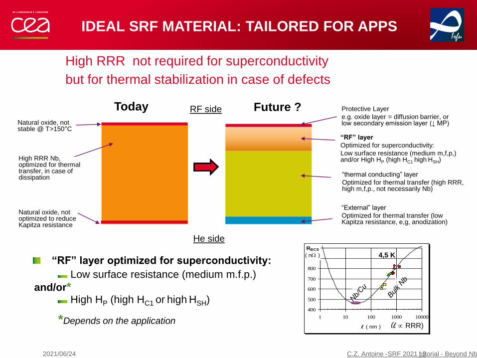
IDEAL SRF MATERIAL: TAILORED FOR APPS
C.Z. Antoine -SRF 2021 tutorial - Beyond Nb| 52021/06/24
Protective Layer
e.g. oxide layer = diffusion barrier, or low secondary emission layer (↓ MP)
“RF” layer
Optimized for superconductivity:
Low surface resistance (medium m,f,p,) and/or High HP (high HC1 high HSH)
“thermal conducting” layer
Optimized for thermal transfer (high RRR, high m,f,p., not necessarily Nb)
“External” layer
Optimized for thermal transfer (low Kapitza resistance, e,g, anodization)
High RRR Nb, optimized for thermal transfer, in case of dissipation
Natural oxide, not stable @ T>150°C
Natural oxide, not optimized to reduce Kapitza resistance
RF side
He side
Today Future ?
“RF” layer optimized for superconductivity:
Low surface resistance (medium m.f.p.)
and/or*High HP (high HC1 or high HSH)
*Depends on the application
400
500
600
700
800
900
1000
1 10 100 1000 10000
l ( nm )
RBCS
( nW )
(l RRR)
4,5 K
High RRR not required for superconductivity
but for thermal stabilization in case of defects
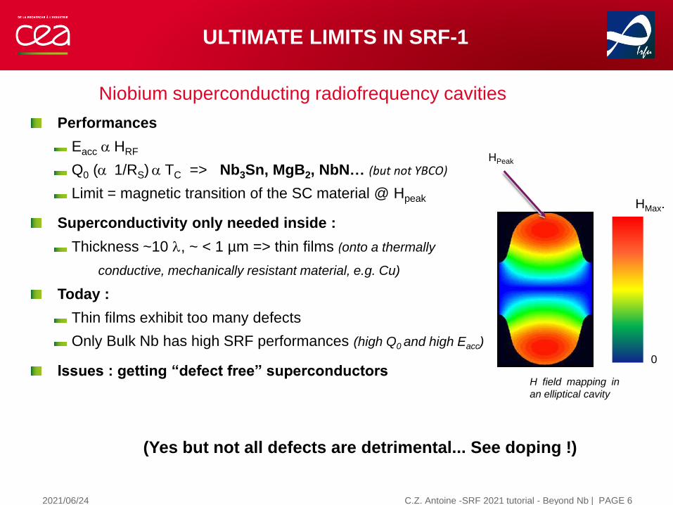
ULTIMATE LIMITS IN SRF-1
Niobium superconducting radiofrequency cavities
Performances
Eacc HRF
Q0 ( 1/RS) TC => Nb3Sn, MgB2, NbN… (but not YBCO)
Limit = magnetic transition of the SC material @ Hpeak
Superconductivity only needed inside :
Thickness ~10 l, ~ < 1 µm => thin films (onto a thermally
conductive, mechanically resistant material, e.g. Cu)
Today :
Thin films exhibit too many defects
Only Bulk Nb has high SRF performances (high Q0 and high Eacc)
Issues : getting “defect free” superconductorsH field mapping in
an elliptical cavity
HPeak
0
HMax.
C.Z. Antoine -SRF 2021 tutorial - Beyond Nb | PAGE 6
(Yes but not all defects are detrimental... See doping !)
2021/06/24

SC phase diagram
All SC applications except SRF: mixed state w. vortex
● Vortices dissipate in RF !
SRF => Meissner state mandatory !
Limit ?
HC1 = limit Meissner/mixed state
● Nb: highest HC1 (180 mT)
Or
HSH “Superheating field”: Metastable state favored by H
// to surface
● Difficult to get in real life !
Surface resistance:
High Tc is better
T<<TC is better ( )
Metallic character in NC state is better ( )
Dirty is better than high RRR ( ) ? (e,g, doping, but more
complex than that !)
HIGH Q0, EACC IN SRF => MEISSNER STATE !
H
T
HC1
HC2
TC
HC
Mixed state w.Vortex
(i.e. N. cond. flux line +
screening currents)
Screening current over l,
no magnetic field deeper
Meissner state
C.Z. Antoine -SRF 2021 tutorial - Beyond Nb | PAGE 7
kT
nFLBCS eT
AR /2
4 ),,,(
l l
n
l
kTe /
2021/06/24

VORTEX PENETRATION WITH B //
C.Z. Antoine -SRF 2021 tutorial - Beyond Nb | PAGE 8
Surface barrier(Bean & Livingston, 1964)
Boundary condition. (J = 0) ≡ “image” vortices
Supercurrent tends to push Vx inside
Image antivortex tends to pull it out
Before entering the material Vx have to cross a surface
barrier:
Vx thermodynamic Potential :
𝐺 𝑥 = 𝜙0 𝐻0𝑒ൗ−𝑥𝜆 −𝐻𝑣 2𝑥 + 𝐻𝐶1 −𝐻0
l
H0
𝑥
J
Image Vortex
J = 0
H0 = Hc1
H0 < Hc1
H0 > Hc1
H0 = Hc
𝑥
G
Meissner
Image
𝑯𝟎 ↗
“Ideal surface”
Barrier disappears only at HSH~HC >HC1
Rationale used to predict SRF limits
BUT
If localized defect w.: Hc𝐿𝑜𝑐𝑎𝑙≪ Hc
𝑏𝑢𝑙𝑘(or Tc
𝐿𝑜𝑐𝑎𝑙≪
Tc𝑏𝑢𝑙𝑘) => early penetration of 1 or several Vx there
2021/06/24

SUPERCONDUCTORS FOR SRF ?
C.Z. Antoine -SRF 2021 tutorial - Beyond Nb | 10
Material TC (K)n
(µWcm)
µ0HC1
(mT)*
µ0HC2
(mT)*
µ0HC
(mT)*
µ0HSH
(mT)*
l
(nm)*
(nm)*
(meV)Type
Pb 7,1 n.a. n.a. 80 48 I
Nb 9,22 2 170 400 200 219 40 28 1.5 II
NbN 17,1 70 20 15 000 230 214 200-350 <5 2.6 II
NbTi 4-13 >11 000 100-200 80-160 210-420 5,4
NbTiN 17,3 35 30 150-200 <5 2.8 II
Nb3Sn 18,3 20 50 30 000 540 425 80-100 <5 <5 II
Mo3Re 15 10-30 30 3 500 430 170 140 II
MgB2 39 0.1-10 30 3 500 430 170 140 5 2.3/7.2 II- 2gaps**
2H-NbSe2 7,1 68 132680-
15000120 95 100-160 8-10 II- 2gaps**
YBCO/Cuprates 93 10 100 000 1400 1050 150 0,03/2 d-wave**
Pnictides
Ba0.6K0.4Fe2As2
38 30 >50000 900 756 200 2 10-20 s/d wave**
* @ 0K
** 2D => orientation problems ?
2021/06/24

WHAT IS THE ACTUAL LIMIT (HP/HC1/HSH) ?
𝑯𝒂𝒑𝒑𝒍
~100 µm in 1 ns (~RF period)
Compare with l (field penetration depth)
Nb : ~ 40 nm
MgB2 ~ 200 nm
Avalanche : high RF dissipation
MgB2: http://www.nature.com/srep/2012/121126/srep00886/full/srep00886.html?message-global=remove&WT.ec_id=SREP-20121127
In real world, cavities behavior is dominated by a few number of defects
It is very important to measure the penetration field of samples in realistic conditions
𝑯𝑹𝑭 𝑯𝑹𝑭
T2T2
C
HC1
HSH
HH//
H
T2T2
C
HC1
HSH
H
H//
H
C.Z. Antoine -SRF 2021 tutorial - Beyond Nb | PAGE 11
Avalanche penetration/flux jumps
2021/06/24
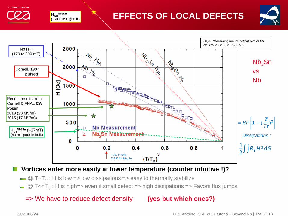
EFFECTS OF LOCAL DEFECTS
Vortices enter more easily at lower temperature (counter intuitive !)?
@ T~TC : H is low => low dissipations => easy to thermally stabilize
@ T<<TC : H is high=> even if small defect => high dissipations => Favors flux jumps
𝐻𝑖 = 𝐻𝑖0 ቈ𝟏 − (𝑻
𝑻𝒄)𝟐
Dissipations :
=> We have to reduce defect density (yes but which ones?)
Nb3Sn
vs
Nb
HC1Nb3Sn (~27mT)
(50 mT pour le bulk)
Recent results from
Cornell & FNAL CW
Posen,
2019 (23 MV/m)
2015 (17 MV/m))
Cornell, 1997
pulsed
Nb HC1
(170 to 200 mT)
HSHNb3Sn
(~ 400 mT @ 0 K)
Hays. "Measuring the RF critical field of Pb,
Nb, NbSn". in SRF 97. 1997.
~ 2K for Nb
3,5 K for Nb3Sn
C.Z. Antoine -SRF 2021 tutorial - Beyond Nb | PAGE 132021/06/24

CHALLENGES TO FACE
ON THE ROUTE TOWARD OTHER
SUPERCONDUCTORS:
GENERALITIES
C.Z. Antoine -SRF 2021 tutorial - Beyond Nb| PAGE 14
GENERAL ISSUES WITH SCs
C.Z. Antoine -SRF 2021 tutorial - Beyond Nb | PAGE 15
Needed: high TC, high HSH
(by defect high HC1)
Advantages of niobium: pure metal.
Highest TC of metallic SC, HC1
Easy to form
Uniform composition, no phase transition in the domain of interest
Very large : makes it less sensitive to small crystalline defects
(e.g. GB)
Issues with alloyed, metallic SC compounds (e.g. NbTi)
Higher TCs, but smaller HC1,
Still relatively easy to form (harder)
Usually several phases, not all of them SC
Risk of non homogeneity
Issues with non metallic SC compounds
Higher TCs, but smaller HC1,
Brittle, no forming is possible, only films (OK for SRF, but a more
complex fabrication route is needed)
Usually several phases, not all of them SC
Risk of non homogeneity
Sometimes local disorder =>
≠ local composition, possibly non SC
Weak links e.g. NC grain boundaries
= main reason why HTC do not apply in SRF .
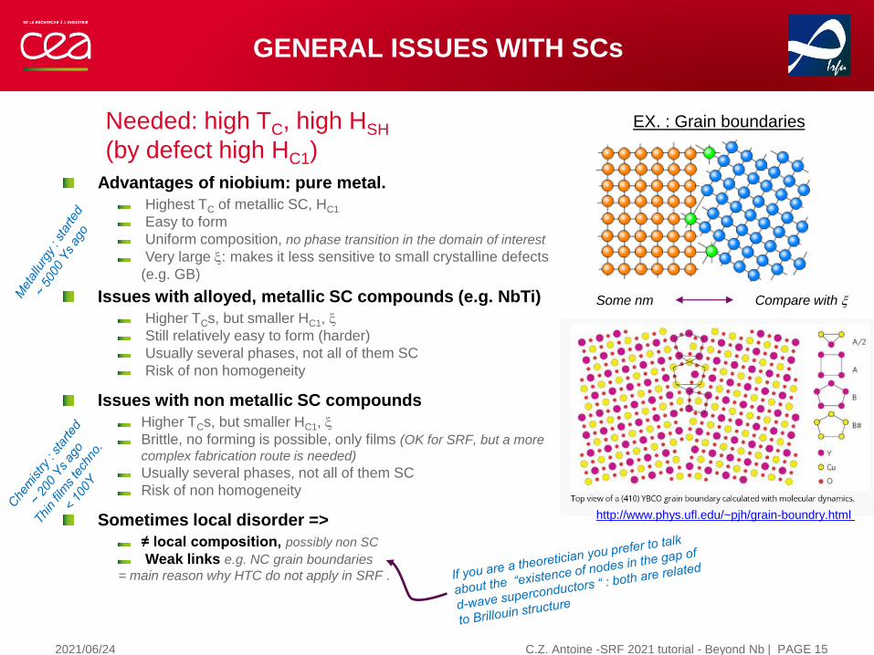
Compare with
EX. : Grain boundaries
Some nm
http://www.phys.ufl.edu/~pjh/grain-boundry.html
2021/06/24

Nb : l~50 nm => only a few 100s nm of SC necessary (the remaining thickness= mechanical
support) => Make thin films !
Advantages
Thermal stability (substrate cavity = copper, Aluminum,… W)
Cost
Opens route to innovative materials
Optimization of RBCS possible (e.g. by playing with m.f.p)
Disadvantages
Fabrication and surface preparation of substrate (at least) as difficult as for bulk Nb
Steep Q0 decrease often observed by increase of RF field (sputtered niobium films, improved lately)
Deposition of innovative materials is very difficult (large parameters space to be explored)
Most of the known SC have been optimized for wire applications (low HC1, defects, pinning
centers… ) => most of the literature recipes are not fitted for SRF application
THIN FILMS DEPOSITION
C.Z. Antoine -SRF 2021 tutorial - Beyond Nb | PAGE 162021/06/24

DEPOSITION TECHNIQUES:
3 MAJORS FAMILIES
Physical deposition techniques (PVD, MS, DS…)
line of sight techniquesissues: getting uniform thickness/structureinternal stress and adhesionlimited for complex geometry
Thermal diffusion films
limited compositions availablenon uniform composition issues (S shaped
diffusion front, differential diffusion rate with substrate grain orientation)
Chemical techniques CVD, ALD
conformational even in complex shapevery quick for large surfacesissues: get the proper crystalline structure
C.Z. Antoine -SRF 2021 tutorial - Beyond Nb | 172021/06/24
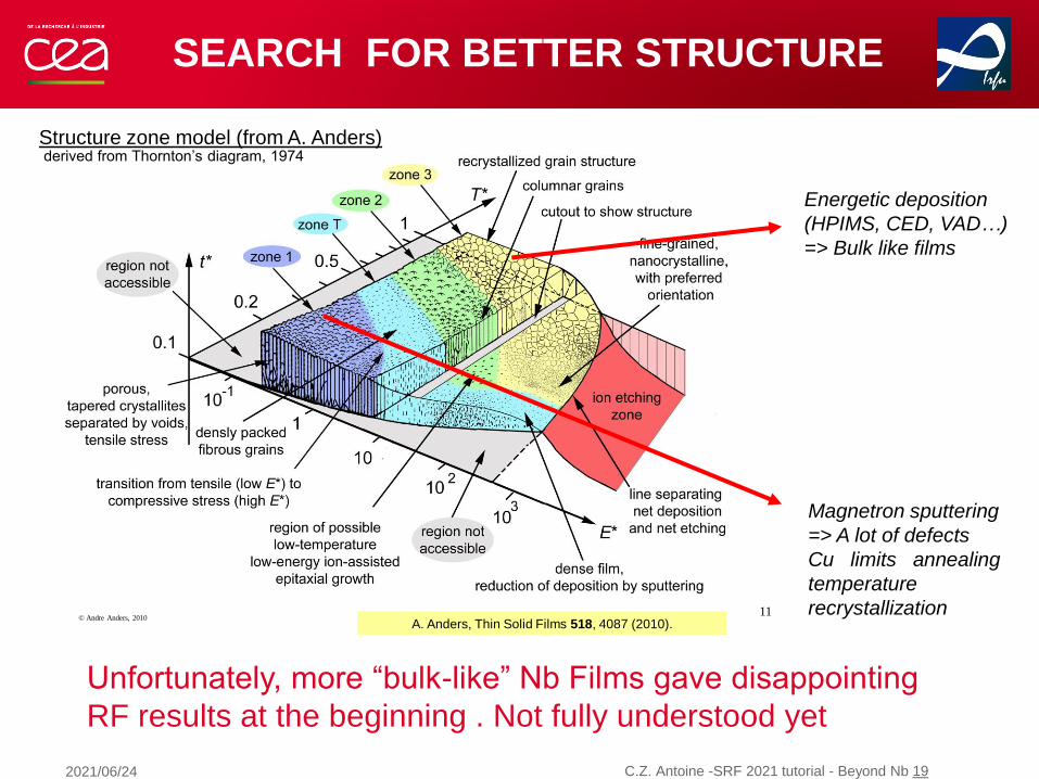
SEARCH FOR BETTER STRUCTURE
© Andre Anders, 201011
Generalized Structure Zone Diagram
A. Anders, Thin Solid Films 518, 4087 (2010).
derived from Thornton’s diagram, 1974
C.Z. Antoine -SRF 2021 tutorial - Beyond Nb 19
Unfortunately, more “bulk-like” Nb Films gave disappointing
RF results at the beginning . Not fully understood yet
Magnetron sputtering
=> A lot of defects
Cu limits annealing
temperature
recrystallization
Energetic deposition
(HPIMS, CED, VAD…)
=> Bulk like films
Structure zone model (from A. Anders)
2021/06/24
Nb/ Cu:
example of the issues
when dealing with thin fims
C.Z. Antoine -SRF 2021 tutorial - Beyond Nb | 212021/06/24

Bulk Nb
1.5 GHz Nb/Cu
1.5 GHz Nb/Cu cavities, sputtered w/ Kr @ 1.7 K (Q0=295/Rs)
LEP II350MHz Nb/Cu (4.2K)
CERN 2000
Nb films – sputtered
SPUTTERED Nb FILMS
C.Z. Antoine -SRF 2021 tutorial - Beyond Nb22
The only Nb films deployed in accelerators were made by
magnetron or diode sputtering (CERN).
Reached relatively low surface fields => Eacc ~ 5 MV/m.
Exponential slope in Rs and Q0
Possible origin of the slope
Depinning of trapped flux
Low HC1
Early vortex penetration due to roughness
Current concentration due to porosities (generating local electrical field)
2021/06/24

EXAMPLE OF QUALITY ISSUES OF FILMS
| 23C.Z. Antoine -SRF 2021 tutorial - Beyond Nb
Line of sight issues => porosities
0° 45° 90°
400 µm
Sensitivity to Cu roughness (the smoother, the better)
Inverted pyramid crystalline growth
Internal stressAdvantage: higher Tc (up to a certain
impurity concentration)
Disadvantage: adhesion issues (peeling)
[G. Rozas]
[M. Ribeaudeau, PhD]
Ra = 0.1 µm
Ra = 0.15 µm
Ra = 0.025 µm
Ra = 0.015 µm
Ra = 0.01 µm
High impurities contentNb = getter material (nearly as good as
Ti => high interstitial content)
Carrier gas incorporation (Ar)
Magn. Sput. Nb
2021/06/24

SUBSTRATE ISSUES
Cu and Nb not miscible (especially in presence of O)
Advantage: low interdiffusion
Disadvantage: adhesion issues (peeling)
Issues on Cu welding arreas
Best results are not always where
expected:
Bulk like films did not perform better !
(but recent changes !!!)
New approaches:
Bulk machining
Electroplating
Laser surfacing …C.Z. Antoine -SRF 2021 tutorial - Beyond Nb | 24
Standard
films
RRRmax =28
Oxide-free
films
RRRmax= 40
[data from CERN +
AM Valente-Feliciano]
2021/06/24

SEAMLESS ISOLDE CAVITY
C.Z. Antoine -SRF 2021 tutorial - Beyond Nb | PAGE 252021/06/24
Local magnetometry on a sample deposited in
the same condition
First evidence of a bulk-like behavior for a thin
film !!!!
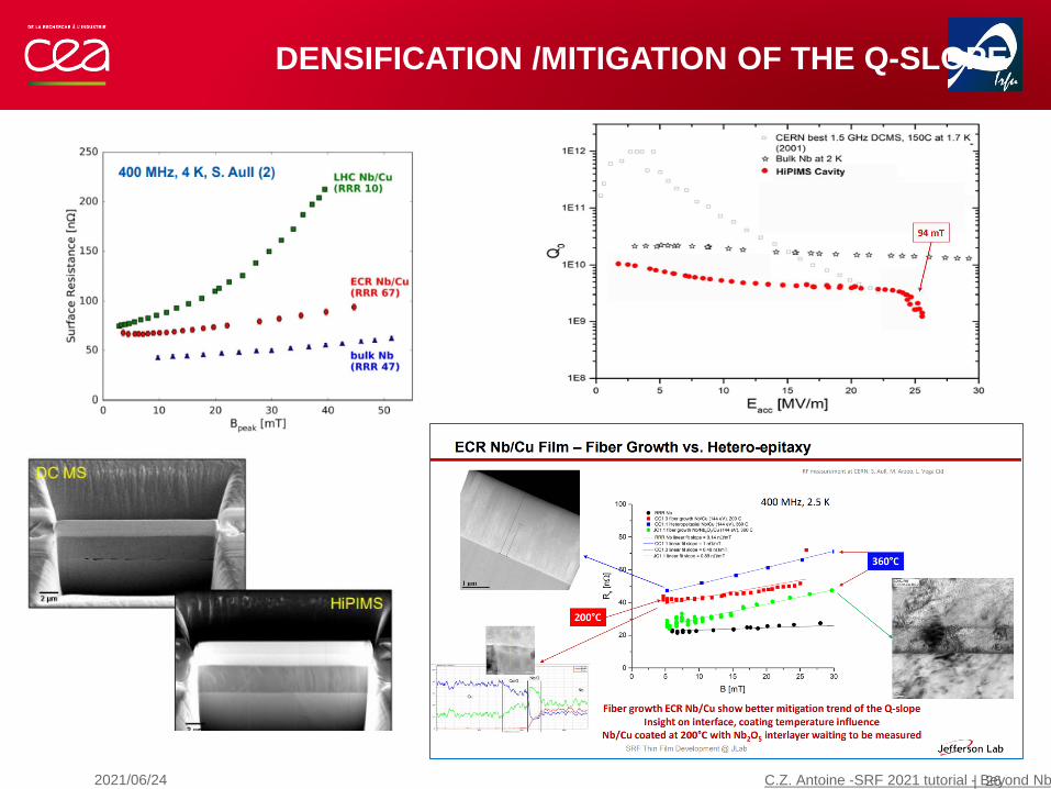
DENSIFICATION /MITIGATION OF THE Q-SLOPE
C.Z. Antoine -SRF 2021 tutorial - Beyond Nb2021/06/24 | 26

| PAGE 28C.Z. Antoine -SRF 2021 tutorial - Beyond Nb
OTHER SUPERCONDUCTORS
2021/06/24
| PAGE 29C.Z. Antoine -SRF 2021 tutorial - Beyond Nb
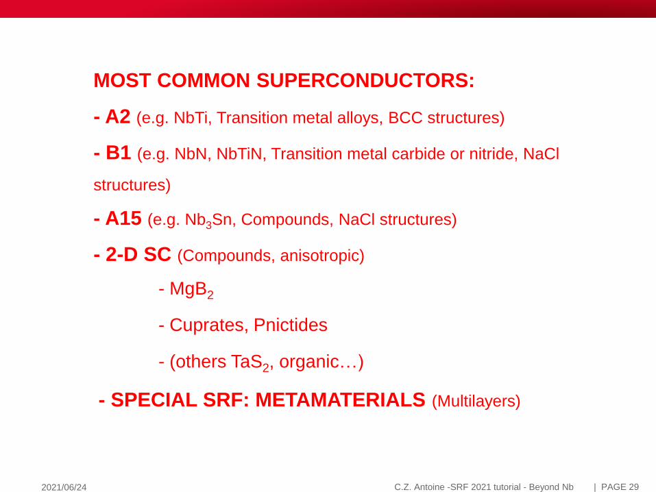
MOST COMMON SUPERCONDUCTORS:
- A2 (e.g. NbTi, Transition metal alloys, BCC structures)
- B1 (e.g. NbN, NbTiN, Transition metal carbide or nitride, NaCl
structures)
- A15 (e.g. Nb3Sn, Compounds, NaCl structures)
- 2-D SC (Compounds, anisotropic)
- MgB2
- Cuprates, Pnictides
- (others TaS2, organic…)
- SPECIAL SRF: METAMATERIALS (Multilayers)
2021/06/24

NbTi widely used in coils
Available alloys range around 45-55 % Ti
Ti is not fully miscible inside Nb (Ti
precipitates ꓱ at low T when [Ti] > 5 W%)
=> no RF !!!
A2 SC ALLOYS: e.g. NbTi
C.Z. Antoine -SRF 2021 tutorial - Beyond Nb | 30
http://www.dierk-raabe.com/titanium-
alloys/biomedical-titanium-alloys/
Ti = Nb
Ti precipitates in a niobium matrix (with a few Nb
replaced by substitutional Ti) => ~ same TC, same HC
as Nb, but not same l => high k
Ti precipitates ( ~0,4 µm)
NC Metal => RF dissipation !!!!
BCC pure metal and solid solution alloy
Ti
2021/06/24

NbN cubic phase : TC ~17-18 K
NbTiN stabilization of cubic (SC) phase
NbN not too sensitive to local variation
of composition !
Solid solution => relatively easy
fabrication (thermal diffusion, reactive sputtering…)
Good model SC
Widely used for JJ and SC electronics
A1 SC COMPOUNDS: e.g. NbN
C.Z. Antoine -SRF 2021 tutorial - Beyond Nb | 31
BCC pure metal + smaller atoms (N, C) in interstitial
location => NaCl structure
https://link.springer.com/content/pdf/10.1007%2F978-1-4757-0037-4.pdf
2021/06/24
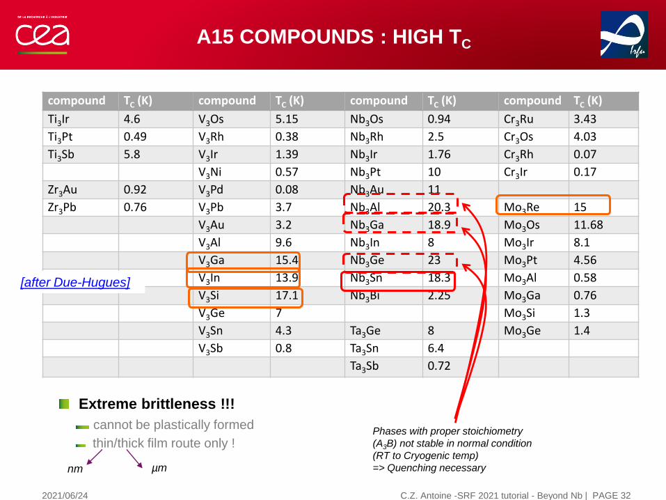
A15 COMPOUNDS : HIGH TC
C.Z. Antoine -SRF 2021 tutorial - Beyond Nb | PAGE 32
compound TC (K) compound TC (K) compound TC (K) compound TC (K)
Ti3Ir 4.6 V3Os 5.15 Nb3Os 0.94 Cr3Ru 3.43
Ti3Pt 0.49 V3Rh 0.38 Nb3Rh 2.5 Cr3Os 4.03
Ti3Sb 5.8 V3Ir 1.39 Nb3Ir 1.76 Cr3Rh 0.07
V3Ni 0.57 Nb3Pt 10 Cr3Ir 0.17
Zr3Au 0.92 V3Pd 0.08 Nb3Au 11
Zr3Pb 0.76 V3Pb 3.7 Nb3Al 20.3 Mo3Re 15
V3Au 3.2 Nb3Ga 18.9 Mo3Os 11.68
V3Al 9.6 Nb3In 8 Mo3Ir 8.1
V3Ga 15.4 Nb3Ge 23 Mo3Pt 4.56
V3In 13.9 Nb3Sn 18.3 Mo3Al 0.58
V3Si 17.1 Nb3Bi 2.25 Mo3Ga 0.76
V3Ge 7 Mo3Si 1.3
V3Sn 4.3 Ta3Ge 8 Mo3Ge 1.4
V3Sb 0.8 Ta3Sn 6.4
Ta3Sb 0.72
[after Due-Hugues]
Extreme brittleness !!!
cannot be plastically formed
thin/thick film route only !Phases with proper stoichiometry
(A3B) not stable in normal condition
(RT to Cryogenic temp)
=> Quenching necessarynm µm
2021/06/24

A15 COMPOUNDS : NARROW DOMAIN OF SC
C.Z. Antoine -SRF 2021 tutorial - Beyond Nb | PAGE 33
A3B
Narrow range of concentration for the SC phase:
Highest TC area is even narrower
Difficult to get uniform SC phase everywhere*
Special issues at grain boundaries: “intrinsic” local deviation of
stoichiometry*
In Nb3Sn wires : GB exhibit degraded SC => weak links, pinning
centersCompare with
Nb3Ga Nb3Al Nb3Ge
B atoms occupy corners and center of BCC structure
A atoms form orthogonal chains bisecting the faces of the BCC unit cell.
Linear Chain Integrity is crucial for Tc (long-range order required)
2021/06/24

Nb3Sn
Special interest for SRF
since the 1980’s
C.Z. Antoine -SRF 2021 tutorial - Beyond Nb | 342021/06/24

Nb3Sn ON Nb (thermal way)
@ 4,2 K: Q0 x 20 compare to Nb, @ 2K ~ the same
Limited in Eacc , best results today ~20 MV/m
Important developments: FNAL, JLAB, CERN, PKU….
C.Z. Antoine -SRF 2021 tutorial - Beyond Nb | 35
[Lieppe, SRF 2013]
Pioneer work: Wuppertal, Cornell
2021/06/24

EFFECTS OF LOCAL DEFECTS
=> We have to reduce defect density (yes but which ones?)
HC1Nb3Sn (~27mT)
(50 mT pour le bulk)
Recent results from
Cornell & FNAL CW
Posen,
2019 (23 MV/m)
2015 (17 MV/m))
Cornell, 1997
pulsed
Nb HC1
(170 to 200 mT)
HSHNb3Sn
(~ 400 mT @ 0 K)
Hays. "Measuring the RF critical field of Pb,
Nb, NbSn". in SRF 97. 1997.
~ 2K for Nb
3,5 K for Nb3Sn
C.Z. Antoine -SRF 2021 tutorial - Beyond Nb | PAGE 36
Nb3Sn
Vs
Nb
2021/06/24
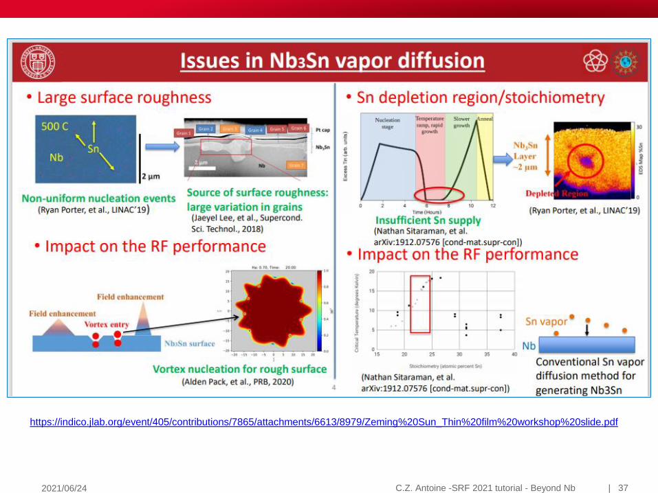
2021/06/24 | 37C.Z. Antoine -SRF 2021 tutorial - Beyond Nb
https://indico.jlab.org/event/405/contributions/7865/attachments/6613/8979/Zeming%20Sun_Thin%20film%20workshop%20slide.pdf

OTHER APPROACHES
C.Z. Antoine -SRF 2021 tutorial - Beyond Nb | PAGE 41
Sputtered Nb3S films on copper
Activities at Cern, STFC, Jlab, Cornell,,,
RT deposited films : right composition but no A15
structure
Heating of substrate (CERN)
And/or post annealing
Other issues
Cracks on the layer (due to differential dilatation coef)
Diffusion of copper in the layer
Carrier gas incorporation (Ar, Kr)
Sn evaporation at higher temperature (> 1000°C)
2021/06/24
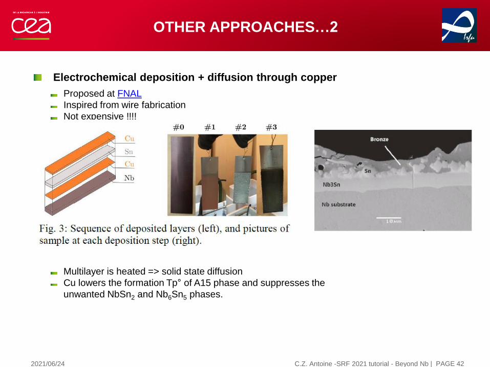
OTHER APPROACHES…2
C.Z. Antoine -SRF 2021 tutorial - Beyond Nb | PAGE 42
Electrochemical deposition + diffusion through copper
Proposed at FNAL
Inspired from wire fabrication
Not expensive !!!!
Multilayer is heated => solid state diffusion
Cu lowers the formation Tp° of A15 phase and suppresses the
unwanted NbSn2 and Nb6Sn5 phases.
2021/06/24
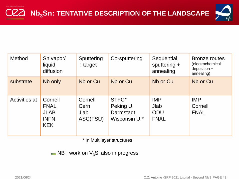
Nb3Sn: TENTATIVE DESCRIPTION OF THE LANDSCAPE
2021/06/24 C.Z. Antoine -SRF 2021 tutorial - Beyond Nb | PAGE 43
Method Sn vapor/
liquid
diffusion
Sputtering
! target
Co-sputtering Sequential
sputtering +
annealing
Bronze routes(electrochemical
deposition +
annealing)
substrate Nb only Nb or Cu Nb or Cu Nb or Cu Nb or Cu
Activities at Cornell
FNAL
JLAB
INFN
KEK
Cornell
Cern
Jlab
ASC(FSU)
STFC*
Peking U.
Darmstadt
Wisconsin U.*
IMP
Jlab
ODU
FNAL
IMP
Cornell
FNAL
* In Multilayer structures
NB : work on V3Si also in progress
| PAGE 44C.Z. Antoine -SRF 2021 tutorial - Beyond Nb
2-D SC (Compounds, anisotropic)
- MgB2
- Cuprates, Pnictides
- Multilayers
2021/06/24

MAGNESIUM DIBORIDE (MgB2)
Graphite-type boron layers
separated by hexagonal close-
packed layers of magnesium
p=2.3meV, 2D, in-plane s-orbital
s=7.1meV 3D, out-of-plane p-orbitals
BCS type superconductor
TC ~40 K, two-gap nature
Advantages:
Very high TC (higher temp operation)
Semimetal, cheap (fertilizer !)
, l of high quality* MgB2 similar to Nb
(~50 nm) (transparency of GB to current flow)
Low n (lower RS)
Disadvantages:
Orientation issues (in polycrystalline materials !)
RF dominated by lower gap !
Still better than Nb :
ΔNb= 1.5 meV < ΔπMgB2= 2.3 meV < ΔNb3Sn= 3.1 meV
<ΔsMgB2= 7.1 meV
Sensitive to H2O (capping necessary ?)
Thin film routes difficult to achieve
* wire quality MgB2: ~1-3 nm, l ~250 nm
(by playing on m.f.p.: crystal structure, grain size, impurities…)
A. Floris et al., cond-
mat/0408688v1 31
Aug 2004
C.Z. Antoine -SRF 2021 tutorial - Beyond Nb | PAGE 452021/06/24

Z.-K. Liu et al., APL 78(2001) 3678.Mg
MgB2
Kinetically limited Mg
MAGNESIUM DIBORIDE (MgB2)
Optimal T for epitaxial growth ~ Tmelt/2
For MgB2 Tmelt/2 = 540°C => PMg ~11 Torr
Too high for UHV deposition techniques (PLD, MBE...)
At PMg = 10-4-10-6 Torr, and Tsub ~ 400°C
Compatible with MBE, and other deposition techniques
MgB2 is stable, but no MgB2 formation:
Mg atoms re-evaporate before reacting with B
At PMg = 10-4-10-6 Torr, and lower T
MgB2 is stable,
If Tsub >250°C, free Mg is lost because the re-
evaporation rate is higher than the impinging rate
If Tsub < 250°C
.Growth rate is very slow,
(kinetically limited by available Mg)
Phase diagram: at low Mg pressure only extremely low
deposition temperatures can be used
evaporation pressure of Mg from
MgB2 < decomposition curve of MgB2
< Mg vapor pressureM. Naito and K. Ueda,
SUST 17 (2004) R1
C.Z. Antoine -SRF 2021 tutorial - Beyond Nb | PAGE 462021/06/24
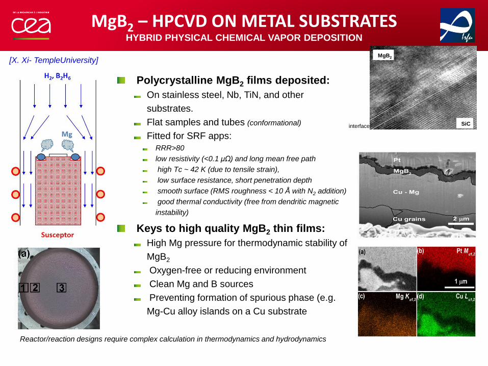
MgB2 – HPCVD ON METAL SUBSTRATESHYBRID PHYSICAL CHEMICAL VAPOR DEPOSITION
[X. Xi- TempleUniversity]
SiC
MgB2
interface
Polycrystalline MgB2 films deposited:
On stainless steel, Nb, TiN, and other
substrates.
Flat samples and tubes (conformational)
Fitted for SRF apps:
RRR>80
low resistivity (<0.1 μΩ) and long mean free path
high Tc ~ 42 K (due to tensile strain),
low surface resistance, short penetration depth
smooth surface (RMS roughness < 10 Å with N2 addition)
good thermal conductivity (free from dendritic magnetic
instability)
Keys to high quality MgB2 thin films:
High Mg pressure for thermodynamic stability of
MgB2
Oxygen-free or reducing environment
Clean Mg and B sources
Preventing formation of spurious phase (e.g.
Mg-Cu alloy islands on a Cu substrate
Reactor/reaction designs require complex calculation in thermodynamics and hydrodynamics

MGB2 – OTHER ROUTE S
Superconducting
Technologies Inc.
RF measurement @ MIT/Lincoln Lab
[T. Tajima, LANL]
In-situ reactive evaporation @ 550˚C
High quality flat samples
Difficult to apply to complex geometries
[R. Valizadeh, STFC]
Plasma electrolytic oxidation (PEO)
MgB2 particles in suspension in an electrolyte
MgB2 Islands deposited on the surface
Issues : homogeneity, purity
To be further explored
C.Z. Antoine -SRF 2021 tutorial - Beyond Nb | 482021/06/24
Nb on
sapphire
MgB2 on
LAO
MgB2 on
sapphire
Oates et al., SUST
23, 034011 (2010)
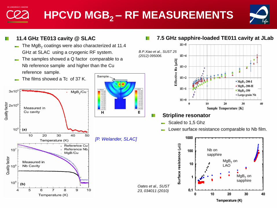
HPCVD MGB2 – RF MEASUREMENTS
11.4 GHz TE013 cavity @ SLAC
The MgB2 coatings were also characterized at 11.4
GHz at SLAC using a cryogenic RF system.
The samples showed a Q factor comparable to a
Nb reference sample and higher than the Cu
reference sample.
The films showed a Tc of 37 K.
7.5 GHz sapphire-loaded TE011 cavity at JLab
Stripline resonator
Scaled to 1,5 Ghz
Lower surface resistance comparable to Nb film.
B.P.Xiao et al., SUST 25
(2012) 095006.
[P. Welander, SLAC]

if ℓ ↗ then:
↗l ↘k ↘ ↘
THE IMPORTANCE OF MEAN FREE PATH, MgB2
EXAMPLE
ℓ mean free path
l~50 nm
~ some 10 nm ?
1
=
1
0+1ℓ
Most developments of HTc are done in view of magnet applications : small high l
by playing with ℓ
Small x makes the superconductors very sensitive to (usual) crystalline defects
(wanted for magnets, not for SRF)
Typical values found in literature for MgB2 : l ~100-150 nm ~ 5-10 nm
2021/06/24 C.Z. Antoine -SRF 2021 tutorial - Beyond Nb | 52
http://mason.gmu.edu/~grobert1/2014syl641.htm
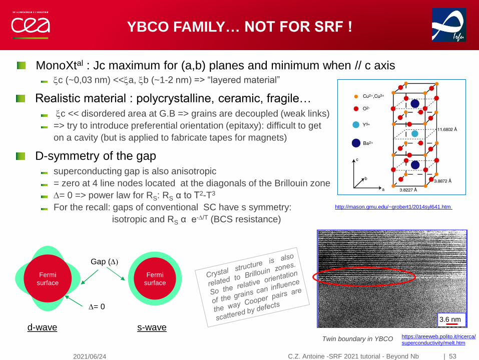
YBCO FAMILY… NOT FOR SRF !
c (~0,03 nm) <<a, b (~1-2 nm) => “layered material”
Realistic material : polycrystalline, ceramic, fragile…
c << disordered area at G.B => grains are decoupled (weak links)
=> try to introduce preferential orientation (epitaxy): difficult to get
on a cavity (but is applied to fabricate tapes for magnets)
D-symmetry of the gap
superconducting gap is also anisotropic
= zero at 4 line nodes located at the diagonals of the Brillouin zone
= 0 => power law for RS: RS α to T2-T3
For the recall: gaps of conventional SC have s symmetry:
isotropic and RS α e-/T (BCS resistance)
3.6 nm
https://areeweb.polito.it/ricerca/
superconductivity/melt.htmTwin boundary in YBCO
Fermi
surface
Fermi
surface
Gap ()
d-wave s-wave
= 0
C.Z. Antoine -SRF 2021 tutorial - Beyond Nb | 532021/06/24
MonoXtal : Jc maximum for (a,b) planes and minimum when // c axis

PNICTIDE FAMILY… MAYBE YES ?
Oxypnictide base: ReOMPn
M = Fe, Co, Ni
Pn = As or P
Re = La, Nd, Sm, Pr
A lot of common with YBCO
High TC (10-55 K up today)
Layered structure
Brittle material
d-wave symmetry observed for some member of the family
But most compounds exhibit s-wave gaps…?
Opening for SRF application ?
C.Z. Antoine -SRF 2021 tutorial - Beyond Nb | 542021/06/24

PNICTIDE FAMILY… MAYBE YES ?
A lot of common with YBCO
High TC (10-55 K up today)
Layered structure
Brittle material
but
Most compounds exhibit s-wave gaps
Very sensitive to impurities content (either magnetic or not)
NaFe1−xCoxAs (x = 0.0175)
= ferromagnetic
NaFe1−xCoxAs (x=0.045)
= SC
~ 5-6 meV
>> Nb3Sn
(3,1meV)
Ba0.6K0.4Fe2As2
C.Z. Antoine -SRF 2021 tutorial - Beyond Nb | 552021/06/24
MULTILAYERS
C.Z. Antoine -SRF 2021 tutorial - Beyond Nb | 572021/06/24
AFTER NIOBIUM : NANOCOMPOSITES
MULTILAYERS
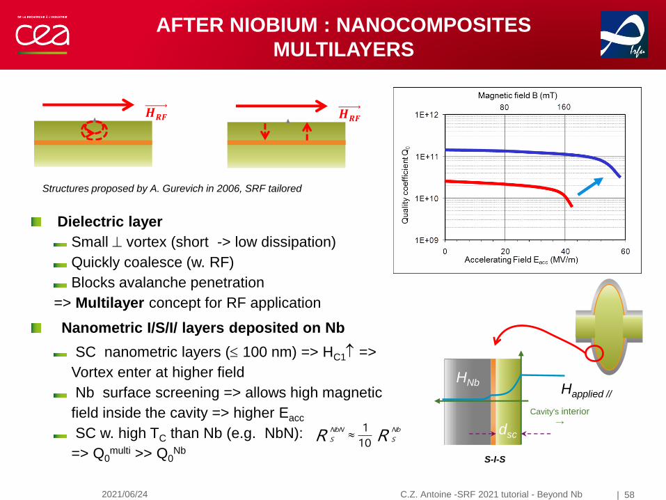
Dielectric layer
Small vortex (short -> low dissipation)
Quickly coalesce (w. RF)
Blocks avalanche penetration
=> Multilayer concept for RF application
Nanometric I/S/I/ layers deposited on Nb
SC nanometric layers ( 100 nm) => HC1 =>
Vortex enter at higher field
Nb surface screening => allows high magnetic
field inside the cavity => higher Eacc
SC w. high TC than Nb (e.g. NbN):
=> Q0multi >> Q0
Nb
Structures proposed by A. Gurevich in 2006, SRF tailored
RRNb
S
NbN
S 10
1
𝑯𝑹𝑭𝑯𝑹𝑭
Cavity's interior→
Happlied //
HNb
S-I-S
dsc
C.Z. Antoine -SRF 2021 tutorial - Beyond Nb | 582021/06/24

d/λ
Maximum screening field Hm at the optimum S thickness dS = dm
FIRST APPROACH: TRILAYERS
Meissner state stable if:
Screening current @ both SC surface is < depairing current
J(0) < Jd = Hs/λ and J(d) < Jd0 = Hs0/λ0
If d is small, HSHS is high, but most of the field reach S0
If d is thicker, HSHS is lower, but screening is more effective
ꓱ an optimum thickness and a maximum screening field!!!
IS S0
d
C.Z. Antoine -SRF 2021 tutorial - Beyond Nb | 592021/06/24

SIS OPTIMIZATION: IMPORTANCE OF MODELS
C.Z. Antoine -SRF 2021 tutorial - Beyond Nb | 61
A. Gurevich, T. Kubo
First approach: trilayers
Boundary conditions implemented (including effect of an
insulating layer. finite thickness))
HSH determined initially in London approx., further
improved w. quasiclassical theory (valid @T<<TC)
Initially assume “perfect conditions”(bulk values, field // to surface)
← Quasiclassical Approach,
Can be further improved…
Previous calculation w. London theory only: not realistic →
[Kubo 2013-17]
Nb3Sn
NbN
225 mT900 mT
Exp decay
w. boundary
cond.
2021/06/24

TRILAYER OPTIMIZATION (…)
C.Z. Antoine -SRF 2021 tutorial - Beyond Nb | 62
A. Gurevich, T. Kubo
Go for realistic condition
Layers present defects, non-negligible surface roughness, non-uniform thickness.
→ HSHS suppressed due to of the local screening current enhancement.
Introducing material suppression factor η =f(defect size and aspect ratio, ξS )
η ~ 0.85 for typical electropolished Nb surface)
HSHSIS and optimal S layer thickness dmS can be determined w. surface topographical data
Nb with defects*,
with BC1=50 mT
* e.g. morphologic
defects that allow earlier
vortex penetration
Ideal Nb substrate
with BC1=170 mT
See exp proof later on
2021/06/24

WHAT IS THE LIMIT (HP/HC1/HSH) ?
Real world cavities behavior is dominated by a few number of defects
It is very important to measure the penetration field of samples in realistic conditions
𝑯𝑹𝑭 𝑯𝑹𝑭
T2T2
C
HC1
HSH
HH//
H
T2T2
C
HC1
HSH
H
H//
H
Local magnetometry
~ Same geometry as cavities
No shape/edge effect (vs DC/
Squid magnetometry)
No demagnetization effect
Measures actual penetration field
wherever it is HP/HC1/HSH
C.Z. Antoine -SRF 2021 tutorial - Beyond Nb | PAGE 632021/06/24
EXPERIMENTAL DETAILS
| PAGE 64C.Z. Antoine -SRF 2021 tutorial - Beyond Nb
T TC
HC1
HMelting
H
HC2
Ia/Ha
Meissner state
Vx lattice
Vx ~ liquid
Low frequency ≡ DC :
0 < Ha< HC1 => R=O, Meissner state
HC1< Ha< HM =>Vx are trapped, R=O, Campbell regime
HM< Ha< HC2 =>Vx are moving liquid like, R≠O, Flux flow regime
Third harmonic signal arise from flux line tension (affects the e-
inside the Cu coil),
It does not depend on dissipation inside Nb, BUT depends on #
of Vx trapped there (and length).
maximum field without Vx (max Eacc)
maximum pinning
flux line moving in AC field
Vx pinned in
the SC
2021/06/24
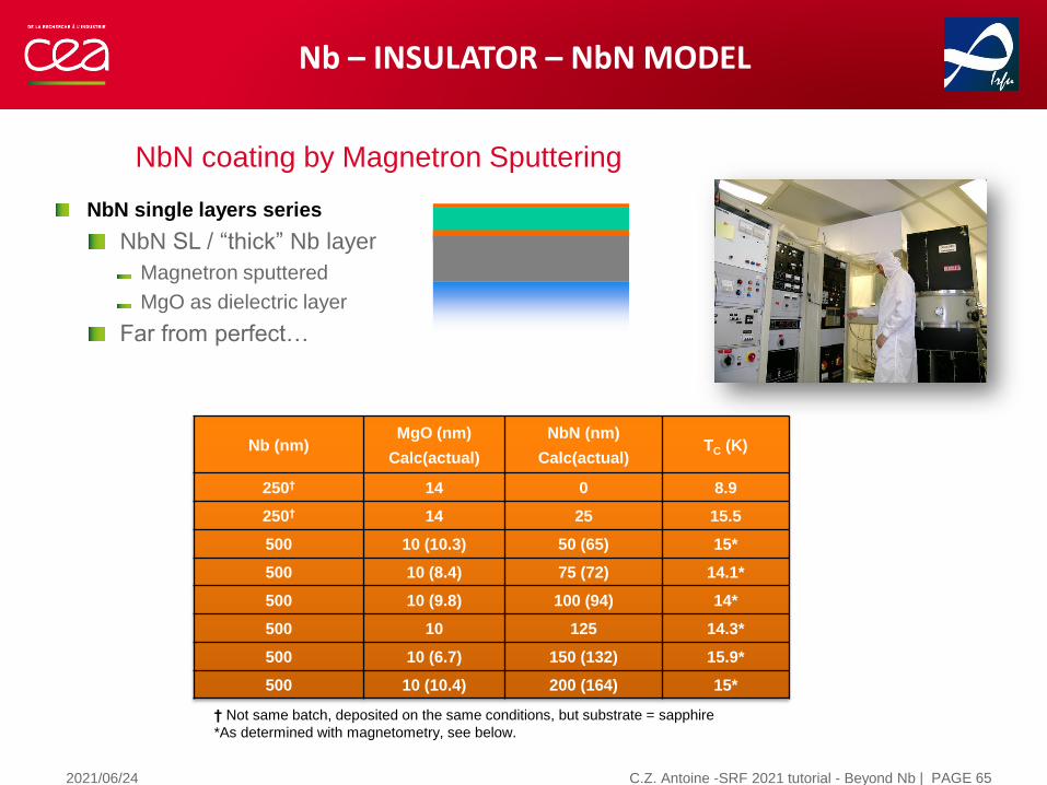
Nb – INSULATOR – NbN MODEL
| PAGE 65C.Z. Antoine -SRF 2021 tutorial - Beyond Nb
NbN coating by Magnetron Sputtering
NbN single layers series
NbN SL / “thick” Nb layer
Magnetron sputtered
MgO as dielectric layer
Far from perfect…
Nb (nm)MgO (nm)
Calc(actual)
NbN (nm)
Calc(actual)TC (K)
250† 14 0 8.9
250† 14 25 15.5
500 10 (10.3) 50 (65) 15*
500 10 (8.4) 75 (72) 14.1*
500 10 (9.8) 100 (94) 14*
500 10 125 14.3*
500 10 (6.7) 150 (132) 15.9*
500 10 (10.4) 200 (164) 15*
† Not same batch, deposited on the same conditions, but substrate = sapphire
*As determined with magnetometry, see below.
2021/06/24
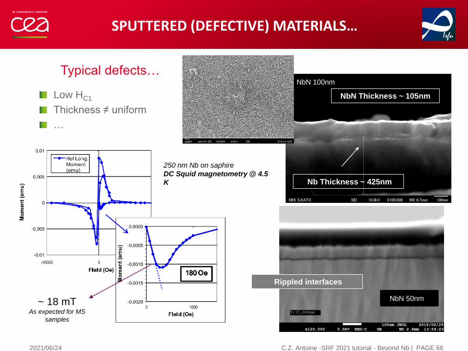
SPUTTERED (DEFECTIVE) MATERIALS…
| PAGE 66C.Z. Antoine -SRF 2021 tutorial - Beyond Nb
Typical defects…
Low HC1
Thickness ≠ uniform
…
Nb Thickness ~ 425nm
250 nm Nb on saphire
DC Squid magnetometry @ 4.5
K
~ 18 mTAs expected for MS
samples
NbN 100nm
NbN Thickness ~ 105nm
NbN 50nm
Rippled interfaces
2021/06/24

COMPARAISON WITH THEORY
| PAGE 68C.Z. Antoine -SRF 2021 tutorial - Beyond Nb
x
x
x
x
x
x
Nb with defects*,
with BC1=50 mT
* e.g. morphologic
defects that allow earlier
vortex penetration See
SST paper cited earlier
Ideal Nb substrate
with BC1=170 mT
x
x
x
x
x
x
Theoritical predictions from T. Kubo (KEK)
0 40 80 120 160 200 240 2800
10
20
30
40
50
60
70
80
Nb
NbN 25nm
NbN 50nm
NbN 75nm
NbN 100nm
NbN 125nm
NbN 150nm
NbN 200nm
Hc1
(m
T)
T2 (K
2)
02 4 6 8 10 12 14 16
T (K)
The enhancement of the field
penetration increases with thickness of
NbN
It reaches a saturation at thicknesses >
100 nm
2021/06/24

COMPARAISON WITH THEORY
| PAGE 69C.Z. Antoine -SRF 2021 tutorial - Beyond Nb
x
x
x
x
x
x
Nb with defects*,
with BC1=50 mT
* e.g. morphologic
defects that allow earlier
vortex penetration See
SST paper cited earlier
Ideal Nb substrate
with BC1=170 mT
x
x
x
x
x
x
Theoritical predictions from T. Kubo (KEK)
0 50 100 150 200 250 3000
10
20
30
40
50
60
70
80
90
100
110
120
130
140
150
Nb
NbN 25nm
NbN 50nm
NbN 75nm
NbN 100nm
NbN 125nm
NbN 150nm
NbN 200nm
According to
2nd transition of V3
Hc1
(m
T)
T2 (K
2)
@ 4.5 K
~ + 110 mT?
~25-30 MV/m
ILC shape
The enhancement of the field
penetration increases with thickness of
NbN
It reaches a saturation at thicknesses >
100 nm
2021/06/24

| PAGE 70C.Z. Antoine -SRF 2021 tutorial - Beyond Nb
6 8
0,00000
0,00002
0,00004
0,00006
0,00008
0,00010
0,00012
V3(V)
Phase(deg)
Temperature(K)
V3(V
)
90
95
100
105
110
115
Phase(d
eg)
4 6 8 10 12 14 16 18
0,00000
0,00002
0,00004
0,00006
0,00008
0,00010
0,00012
V3(V)
Phase(deg)
Temperature(K)
V3(V
)
-100
-50
0
50
100
150
Phase(d
eg)
Voltage signal
6 8
0,00004
V3(V)
Phase(deg)
Temperature(K)
V3(V
)
-100
-50
0
50
100
150
Phase(d
eg)
Phase signal1
2
T~TT>>T
For a given Happl, we observe 3
≠ transition temperatures
3
T~T: within noise level
T>>T: dramatic transition
CLOSEUP OF 3rd HARMONIC SIGNAL
2021/06/24

Thin SC layer NbN
Insulator MgO
Thick SC layer Nb
ROLE OF THE DIELECTRIC LAYER !
| PAGE 71
H // surface => surface
barrier†
A defect locally weakens
the surface barrier
1st transition, vortex
blocked by the insulator
~100 nm => low dissipation.
2nd transition, propagation
of vortex avalanches (~100
µm) => high dissipation.
Dielectric layer = efficient
protection !!!
Why do we have two transitions ?
Defect
H app
Field lines
First transition
Second transition
C.Z. Antoine -SRF 2021 tutorial - Beyond Nb2021/06/24

SIS : IRREVERSIBILITY => NO VORTEX
PINNING <= NO VX ENTRY ?
| PAGE 73
Longitudinal moment (Zoom)
Comparison Sample SL with reference R-SL
-2,00E+05
-1,00E+05
0,00E+00
1,00E+05
2,00E+05
-7,E+05 -5,E+05 -3,E+05 -1,E+05 1,E+05 3,E+05 5,E+05 7,E+05
Field (A/m)
Mo
men
t (n
orm
alis
ed)
SL
R-SL
Longitudinal moment (Zoom)
Comparison Sample SL@ 4,5 K/@ 12 K
-4,00E+05
-3,00E+05
-2,00E+05
-1,00E+05
0,00E+00
1,00E+05
2,00E+05
3,00E+05
4,00E+05
-7,E+05 -5,E+05 -3,E+05 -1,E+05 1,E+05 3,E+05 5,E+05 7,E+05
Field (A/m)
Mo
men
t (n
orm
alis
ed)
SL @ 4,5 K
SL @12 K
H // sample plane; longitudinal moment
4.5 KNb/MgO/NbN 25 nm
HP~95 mT
Nb 500 nm =
ref
HP~18 mT
Nb/MgO/NbN 25 nm @ 4.5 K
Nb/MgO/NbN 25 nm @ 12 K
C.Z. Antoine, et al
http://accelconf.web.cern.ch/accelconf/S
RF2009/papers/tuppo070.pdf
Each individual layer : defects, but combination: seems protected
SIS : an intrinsically safe structure ?
Nb3Sn
AlN
Nb thick
Cu
[Curtesy R.
Valizadeh and E.
Seiler, 2019]
2021/06/24 C.Z. Antoine -SRF 2021 tutorial - Beyond Nb
0
1
2
3
4
5
6
7
8
0 1 2 3 4 5
Rs
(µO
hm
)
T(K)
Rs = f(T)
Rs(ML4)
Rs(Nb) (scalingin w2)
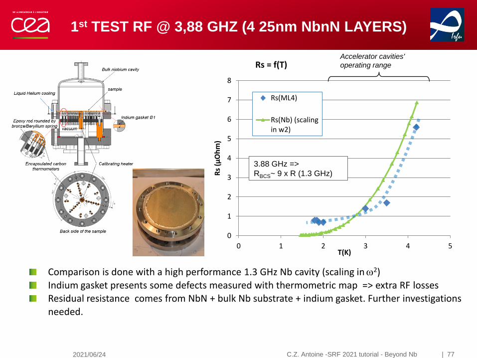
1st TEST RF @ 3,88 GHZ (4 25nm NbnN LAYERS)
Accelerator cavities'
operating range
Comparison is done with a high performance 1.3 GHz Nb cavity (scaling in 2)
Indium gasket presents some defects measured with thermometric map => extra RF lossesResidual resistance comes from NbN + bulk Nb substrate + indium gasket. Further investigations
needed.
3.88 GHz =>
RBCS~ 9 x R (1.3 GHz)
C.Z. Antoine -SRF 2021 tutorial - Beyond Nb | 772021/06/24

C.Z. Antoine -SRF 2021 tutorial - Beyond Nb | 78
[A.M.Valente-Feliciano]
2021/06/24

The SS boundary provides an additional barrier to prevent penetration of
vortices. It would not be as robust as the I layer of the SIS structure, but it also
contributes to pushing up the onset of vortex penetration.
ML WITHOUT DIELECTRIC INTERLAYER
[Kubo, SST]
C.Z. Antoine -SRF 2021 tutorial - Beyond Nb | 79
[Junginger, SRF 2017]
µ-SR
2021/06/24

CONCLUSIONS AND PERSPECTIVES
Superconducting cavities are dominated by their surface quality (Niobium
AND other SC !)
Niobium is close to its ultimate limits, but can be surface tailored (doping)
HSH difficult to reach in real “accelerator cavities” (low T, large scale cavity
fabrication, surface defects,…)
ML structures seem to be a promising way to go toward realistic complex
materials (+ Nb cavity upgrade)
Renewed activity on bulk-like Nb films (cost issues) and high HSH SC e.g.
Nb3Sn or NbN (higher performances)
Look for higher Q0, not only Eacc !
WE ARE ON THE EVE OF A TECHNOLOGICAL REVOLUTION FOR SRF
CAVITIES !
C.Z. Antoine -SRF 2021 tutorial - Beyond Nb | 802021/06/24