Material Matters Volume 1, Number 3
20
2006 VOLUME 1 NUMBER 3 sigma-aldrich.com Indispensable in Space and on Earth – ceramic films in action. Chemical Deposition Techniques in Materials Design Savannah ALD System Sol-Gel Science for Ceramic Materials Hermetic Barrier Using Vinyl Triethoxysilane (VTEOS) Silicon-Based Passive and System-in-Package Integration Vacuum Deposited Non- Precious Metal Catalysts for PEM Fuel Cells TM Deposition of Ceramic and Hybrid Materials
Transcript of Material Matters Volume 1, Number 3

2006VOLUME 1NUMBER 3
sigma-aldrich.com
Indispensable in Space and on Earth – ceramic films in action.
Chemical Deposition Techniques in Materials Design
Savannah ALD System
Sol-Gel Science for Ceramic Materials
Hermetic Barrier Using Vinyl Triethoxysilane (VTEOS)
Silicon-Based Passive and System-in-Package Integration
Vacuum Deposited Non-Precious Metal Catalysts for PEM Fuel Cells
TM
Deposition of Ceramic and Hybrid Materials
si
gm
a-
al
dr
ic
h.
co
m
�
Vol. 1 No. 3
Aldrich Chemical Co., Inc. Sigma-Aldrich Corporation6000 N. Teutonia Ave.Milwaukee, WI 53209, USA
To Place Orders
Telephone 800-325-3010(USA)FAX 800-325-5052(USA)
Customer & Technical Services
CustomerInquiries 800-325-3010TechnicalService 800-231-8327SAFC™ 800-244-1173CustomSynthesis 800-244-1173Flavors&Fragrances 800-227-4563International 414-438-385024-HourEmergency 414-438-3850WebSite sigma-aldrich.comEmail [email protected]
Subscriptions
TorequestyourFREEsubscriptiontoMaterial Matters,pleasecontactusby:
Phone: 800-325-3010(USA)
Mail: Attn: Marketing Communications Aldrich Chemical Co., Inc. Sigma-Aldrich Corporation P.O. Box 355 Milwaukee, WI 53201-9358
Email: [email protected]
International customers, please contact yourlocal Sigma-Aldrich office. For worldwide contactinformation,pleaseseebackcover.
Material Matters is also available in PDF format ontheInternetatsigma-aldrich.com/matsci.
Aldrich brand products are sold through Sigma-Aldrich, Inc. Sigma-Aldrich, Inc. warrants that itsproducts conform to the information contained inthisandotherSigma-Aldrichpublications.Purchasermustdetermine thesuitabilityof theproduct for itsparticularuse.Seereversesideofinvoiceorpackingslipforadditionaltermsandconditionsofsale.
Allpricesaresubjecttochangewithoutnotice.
Material Matters is a publication ofAldrich ChemicalCo., Inc. Aldrich is a member of the Sigma-AldrichGroup.©2006Sigma-AldrichCo.
TM
Intr
od
uct
ion
About Our Cover
The need for films and coatings is ubiquitous in the technological age we live. For example, films serving as humidity barriers form an essential part of microelectronics, micro-electromechanical systems and energy conversion devices. The cover depicts a molecule of vinyl triethoxysilane (VTEOS) that could be used to make a barrier film by chemical deposition. VTEOS is a multifunctional molecule that enables the generation of a hybrid silicon oxide film with polymerizable vinyl groups; the inorganic content is designed to be the barrier, while the hydrophobic, organic content repels water and fills porosity; for more details, please refer to the article by the Rutgers research group on page 11. As alluded to on the cover, such a film could be used to seal the elements of solar panels on a geosynchronous satellite for protection from the external environment.
IntroductionWelcome to the third issue of Material MattersTM. This issue focuses on chemical deposition techniques and their application in electronics and alternative energy.
An introduction and comparison of chemical vapor deposition and solution deposition approaches to film fabrication is given by Dr. Balema of Sigma-AldrichTM Materials Science. Scientists from Cambridge NanoTech discuss Chemical Vapor Deposition (CVD) and Atomic Layer Deposition (ALD), as well as advantages of the Savannah ALD system. Dr. Young from the US Army Research Laboratory highlights basics of sol-gel science for ceramic materials. The group of Prof. Klein from Rutgers University presents a paper on the development of a hermetic barrier using vinyl triethoxysilane (VTEOS) via Sol-Gel Processing. Dr. Roozeboom from Philips and Prof. Kessels from the University of Technology, Eindhoven, Netherlands, discuss the suitability of atomic layer deposition in the fabrication of Si-based integrated passives and System-in-Package integration. Finally, researchers from the 3M Company led by Dr. Atanasoski and Dr. O’Neill report on the use of vacuum deposition in the preparation of electrode materials for fuel cells. Products that accelerate your research in the fundamental and applied science of chemical deposition are highlighted. We invite your comments, questions and suggestions about Material MattersTM and materials of interest to you: [email protected].
Coming Soon!
Reserve your FREE set today.
NEW Aldrich Handbook
RESEARCH IS EASIER WHEN yOU USE THE RIGHT TOOLS!
Visit sigma-aldrich.com/handbook19
Catalog Cover: The Alchemist (ca. 1937) by Newell Convers Wyeth. Courtesy of the Chemical Heritage Foundation Image Archives.
Aldrich Handbook of Fine Chemicals
Set Includes the NEWSigma-AldrichLabware Catalog
Featuring: • Chemical Solution Deposition/Sol-Gel Processing • Chemical Vapor Deposition • Conducting Polymers • Fuel Cells • Materials for Hydrogen Storage • Proton Exchange Membrane (PEM) Material • Nanoparticles • Nanopowders & Nanodispersions • Functionalized Nanoparticles • Quantum Dots • Electronic Grade Materials
Enhanced Application Index includes Materials Science.
35,000 Material Listings 2,000 NEW Products6,100 Citations 3,000 Application NotesEnhanced Application Index Advanced Product Tables
(Shipping January 2007)
For questions, product data, or new product suggestions, please contact the Materials Science team at [email protected].
Or
de
r:
1
.8
00
.3
25
.3
01
0
Te
ch
ni
ca
l
Se
rv
ic
e:
1
.8
00
.2
31
.8
32
7
3C
hem
ical D
ep
ositio
n
Tech
niq
ues
Materials with a layer thickness below 1 µm are called thin films, while thicker layers, especially those exceeding dimensions of a transistor in an electronic chip, are defined as thick films. Both thin and thick films play an exceptionally important role as elements of electronic and optical devices, computer memory chips, and in other related applications. Additionally, in the case of ceramic films, properties such as chemical resistivity and hardness enable their use as coatings on substrate materials and cutting tools for protection against corrosion, oxidation, and wear.
Typically, CVD/ALD techniques are methods of choice for the deposition of thin films on inorganic substrates, while solution-based sol-gel approaches are considered when thick films or nano-powders are desired. Also, lower equipment cost and reasonably good conformality of coatings may make sol-gel a low-cost alternative to CVD/ALD. However, the ALD approach may be required for the preparation of uniform conformal films on complex surfaces such as those with high aspect ratios.
Usually, the nature of the deposition process determines the way in which the thickness of the film is controlled. Thus, in conventional CVD, the film growth depends on the deposition time, while in ALD it is controlled by the number of deposition cycles.1-3 In sol-gel processing, the films are created using two major approaches – spin coating or dip coating. In the first case, the substrate is spun at an angular speed ω and the precursor (sol) is directed onto its surface along the rotation axis. The thickness (h) of the created films depends on a complex combination of the sol’s properties and the rotation speed of the substrate. In practice, they can be predicted using a semi-empirical formula
h = AωΒ
where A and B are empirical coefficients. The dip coating process consists of the successive dipping and withdrawal of the substrate in and out of the solution. The thickness of the film obtained in one dipping-withdrawal cycle is determined8 by the properties of the solution, i.e. viscosity (η), density (ρ), surface tension (σ) and the withdrawal speed (n) :
h = 0.945{(nη)2/3/ (gρ)1/2σ1/6}
While CVD/ALD techniques produce thin films of high uniformity and metal purity, sol-gel processing provides a unique and simple approach to tuning the film’s chemical composition and morphology. Sol-gel processing can also offer a less expensive alternative to CVD/ALD, especially if in situ doping is required.
An example, when solution processing has been used successfully as an alternative to CVD/ALD was in the preparation of silicon thin-film transistors where the deposition of a polycrystalline silicon used a liquid precursor, cyclopentasilane (Si5H10).
9 The grain size in the films obtained were found to be as low as 300 nm, comparable to that for films typically prepared by CVD.
Dr. Viktor P. Balema Sigma-Aldrich Materials Science
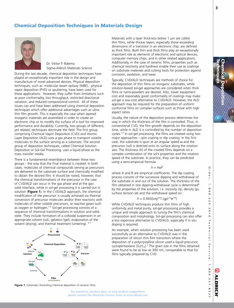
During the last decade, chemical deposition techniques have played an exceptionally important role in the design and manufacture of novel advanced devices. Physical deposition techniques, such as molecular beam epitaxy (MBE), physical vapor deposition (PVD) or sputtering, have been used for these applications. However, they suffer from limitations such as poor conformality, low throughput, restricted directional variation, and reduced compositional control. All of these issues can and have been addressed using chemical deposition techniques which offer additional advantages such as ultra-thin film growth. This is especially the case when layered inorganic materials are assembled in order to create an electronic chip or to modify the surface of a tool for improved performance and durability. Currently, two groups of different, yet related, techniques dominate the field. The first group comprising Chemical Vapor Deposition (CVD) and Atomic Layer Deposition (ALD) uses a gas phase to transport volatile molecules to the surface serving as a substrate. The second group of deposition techniques, called Chemical Solution Deposition or Sol-Gel Processing, uses a liquid phase as the mass transfer media.
There is a fundamental resemblance between these two groups - the way that the final material is created. In both cases, molecules of chemical compounds serving as precursors are delivered to the substrate surface and chemically modified to obtain the desired film. It should be noted, however, that the chemical transformations of the precursor in the case of CVD/ALD can occur in the gas phase and at the gas-solid interface, while in sol-gel processing it is carried out in solution (Figure 1). In the CVD/ALD approach, the chemical modification of the precursor is usually achieved via thermal conversion of precursor molecules and/or their reactions with molecules of other volatile precursors, or reactive gases such as oxygen or hydrogen.1-3 Sol-gel processing consists of a sequence of chemical transformations in solution and solid-state. They include formation of a colloidal suspension in an appropriate solvent (sol), gelation (gel), evaporation of the solvent (drying), and thermal treatment (sintering). 4-7
Sol
Gel
Xerogel
Film
Precursor(s)
ALDCVD
ALD
ALD
CVD
CVD
Sintering
Drying
Gelation
Chemical Deposition
Solution Vacuum
Figure 1. Schematic illustrating chemical deposition of ceramic films.
Chemical Deposition Techniques in Materials Design

TO ORDER: Contact your local Sigma-Aldrich office (see back cover), call 1-800-3�5-3010 (USA), or visit sigma-aldrich.com/matsci.s
ig
ma
-a
ld
ri
ch
.c
om
�C
hem
ical
Dep
osi
tio
n
Tech
niq
ues
An illustration where CVD is clearly preferred over solvent-based processing, is the deposition of magnesium aluminum spinel (MgAl2O4). Magnesium aluminum spinel is an excellent material for refractory applications because of its mechanical strength, chemical resistance, and low density. Also, it shows potential as a humidity sensor and as a buffer layer for the growth of oxide superconductors. Thin films of MgAl2O4 have been successfully prepared by CVD using Mg-Al precursors such as MgAl2(OPr-i)8 or MgAl2(OBu-t)8. Sol-gel processing was employed for this application using a similar intermediate, MgAl2[(OCH2CH2)N]3, resulting in micro-porous powders.10,11 Remarkably, certain groups of precursors, such as metal alkoxides, for example, can be used successfully in both CVD/ALD and Chemical Solution Deposition/Sol-Gel Processing of metal-oxide films and nano-structures.12-14
Thus, when used to the best of their abilities, Chemical Vapor and Solution Deposition techniques are excellent tools, to enable the design of a broad range of materials with pre-defined dimensions, morphology and properties.
Acknowledgements I would like to thank Dr. S. Jasty, Dr.A.Korolev, Dr. M. Stender, and S. Adam for discussions and help in the preparation of the manuscript.
References:(1) D.M. Dobkin and M.K. Zuraw, Principles of Chemical Vapor Deposition: What’s Going on Inside the Reactor, �003, Kluwer Academic Publishers, Boston, Dodrecht, London. (2) R. Fischer, Precursor Chemistry of Advanced Materials, �005, Springer, New York. (3) D. Monsma, J. Becker, Material Matters, �006, Vol. 1, No. 3, 5. (4) S.K.Young’s, Material Matters, �006, Vol 1., No. 3, 8.(5) F. Caruso, Colloids and Colloid Assemblies: Synthesis, Modification, Organization, and Utilization of Colloid Particles, �00�, John Wiley & Sons, New York. (6) Sol-Gel Technology for Thin Films, Fibers, Preforms, Electronics, and Specialty Shapes, L.C. Klein, Ed., 1988, Noyes Publ., Park Ridge, NJ. (7) A.C.Pierre, Introduction to Sol-Gel Processing, �00� Kulwer Academic Publishers, Boston, Dodrecht, London. (8) V. Kiisk, Optical Investigation of Metal-Oxide Films, �006, Tartu University Press, Tartu. (9) T. Shimoda, Y. Matsuki, M. Furusawa, T. Aoki, I. Yudasaka, H. Tanaka, H. Iwasawa, D. Wang, M. Miyasaka, Y. Takeuchi, Nature, �006, 440, 783. (10) K.F.Waldner, R.M.Laine, S. Dhumrongvaraporn, S.Tayaniphan, R.Narayanan, Chem. Mater. 1996, 8, 2850 (11) S.Mathur, M.Veith, T.Ruegamer, E.Hemmer, H.Shen, Chem. Mater. �00�, 16, 1304. (12) N. Lecerf, S. Mathur, H. Shen, M. Veith, S. Huefner, Scripta Mater. �001, 44, 2157 (13) M. Veith, J. Chem. Soc., Dalton Trans., �00�, 2405 (14) L.G. Hubert-Pfalzgraf, Inorg. Chem. Communications �003, 6, 102.
High-Purity Metal Alkoxides
Metal Precursor Linear Formula Purity (%) Product No.
Aluminum Aluminum isopropoxide Al[OCH(CH3)2]3 99.99 ��9�07-10G
��9�07-50G
��9�07-�50G
Aluminum-tri-sec-butoxide Al[OCH(CH3)C2H5]3 99.99 511609-5G
Germanium Germanium(IV) ethoxide Ge(OC2H5)4 99.95 339180-1G
339180-5G
339180-�5G
Hafnium Hafnium(IV) n-butoxide 99 6679�3-�5G
Tetrakis(1-methoxy-2-methyl-2 propoxy)hafnium(IV) Hf(OC(CH3)2CH2OCH3)4 99.99 568171-10G
568171-�5G
Magnesium Magnesium ethoxide Mg(OC2H5)2 98 �918�6-5G
�918�6-100G
Niobium Niobium(V) ethoxide Nb(OCH2CH3)5 99.95 339�0�-5G
339�0�-50G
Tin Tin(IV) tert-butoxide Sn(OC(CH3)3)4 99.99 �9�135-5G
�9�135-�5G
Tantalum Tantalum(V) ethoxide Ta(OC2H5)5 99.98 339113-10G
339113-100G
Titanum Titanium(IV) isopropoxide Ti[OCH(CH3)2]4 99.999 377996-5ML
377996-�5ML
377996-100ML
Titanium(IV) methoxide Ti(OCH3)4 99.99 �6358�-�5G
Tungsten Tungsten(VI) ethoxide 99 667935-�G
667935-10G
Zirconium Zirconium(IV) diisopropoxidebis(2,2,6,6-tetramethyl-3,5-
heptanedionate)
Zr(OCC(CH3)3CHCOC-
(CH3)3)2(OC3H7)2
99.99 �9�151-5G
�9�151-�5G
Zirconium(IV) isopropoxide isopropanol complex Zr(OCH(CH3)2)4 · (CH3)2CHOH
99.9 339�37-10G339�37-50G
Zirconium(IV) tert-butoxide electronic grade Zr[OC(CH3)3]4 99.999 560030-5G
560030-�5G

For questions, product data, or new product suggestions, please contact the Materials Science team at [email protected].
Or
de
r:
1
.8
00
.3
25
.3
01
0
Te
ch
ni
ca
l
Se
rv
ic
e:
1
.8
00
.2
31
.8
32
7
5
The S
avan
nah
ALD
Syste
m
Dr. Douwe Monsma and Dr. Jill Becker
Cambridge NanoTech Inc.
IntroductionAtomic Layer Deposition (ALD) is a coating technology that allows perfectly conformal deposition onto complex 3D surfaces. The reason for this uniform coating lies in the saturative chemisorption of sequential cycles of precursor vapors. The process is illustrated in Figure 1. In Figure 1a, a silicon surface is terminated with hydroxyl groups (formed during contact with air). The wafer is inserted in an ALD reactor and a first precursor is introduced (here trimethyl aluminum, TMA, Figure 1a-b) using a fast pulse valve to a cylinder with liquid TMA. The precursor reacts with the surface layer, but not with itself, forming a single saturated monolayer. Subsequently, the TMA vapor and methane reaction products are pumped away and water vapor is introduced (Figure 1c-d). This forms a saturated monolayer of oxygen (Figure 1e) with a volatile reaction product of methane (again a saturated monolayer because the water molecules don’t react anymore after the water formed the hydroxyl (OH) passivated surface). The methane and water are pumped away and the cycle is repeated until the desired coating thickness is obtained (Figure 1f).
a b
c d
e f
Figure 1a-f. Atomic Layer Deposition reaction cycle showing the formation of Al2O3 coating using trimethylaluminum (TMA) and water as precursors, and methane as volatile reaction product.
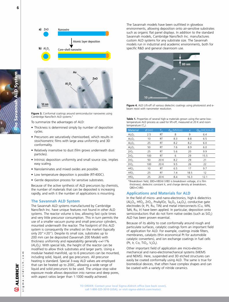
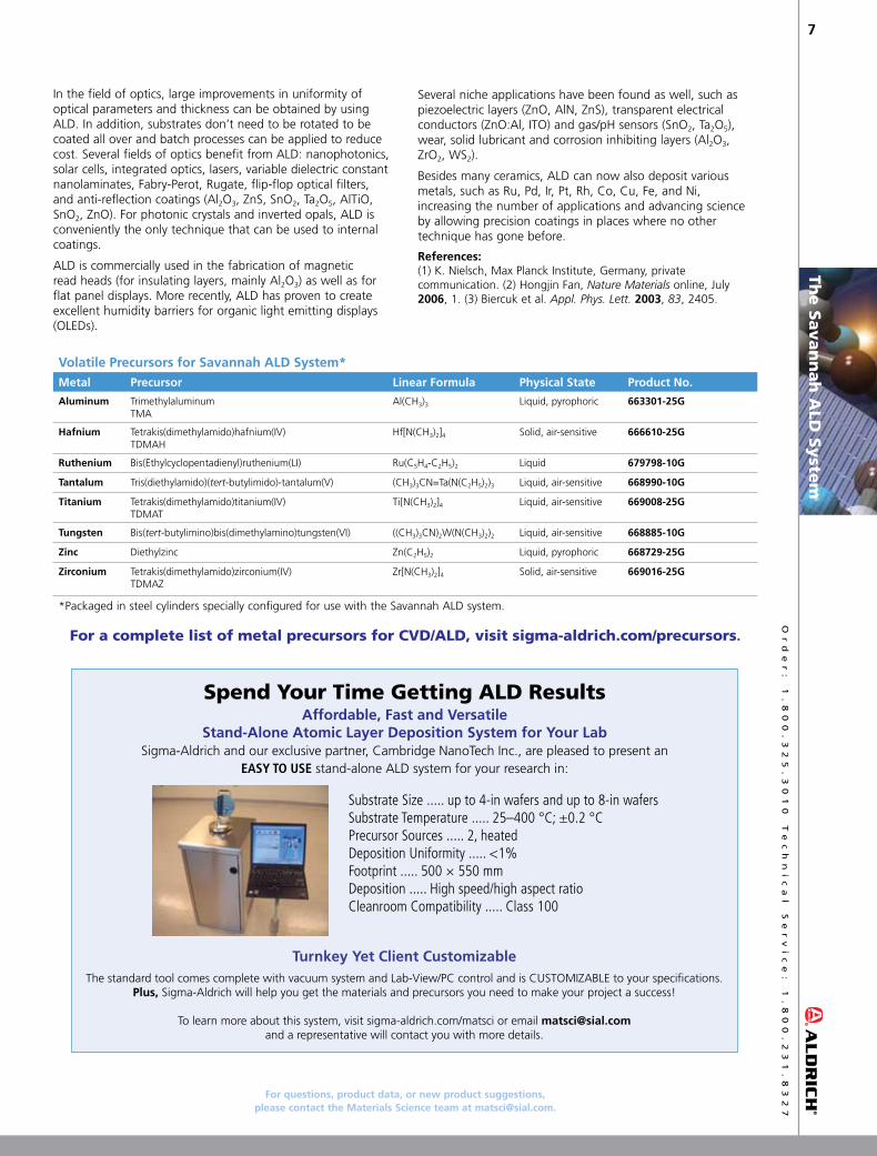
Since the films saturate to a monolayer with each precursor pulse, the coating will be equally thick inside small pores as on the surface of a substrate. This allows deposition inside photonic crystals, DRAM capacitor trenches, around suspended MEMS structures, around particles, etc. In fact, aspect ratios larger than 1:1000 can be routinely achieved using Cambridge NanoTech ALD systems; an example is shown in Figure � where a uniform coating is formed inside 50 nm dia, 50 micron deep pores in anodically etched aluminum oxide substrates and in Figure 3 where semiconductor nanowires have been coated conformally. For microelectronic applications, we have demonstrated lift-off of ALD coatings with nanometer resolution (Figure �). Here we either used optical resist or e-beam resist to form patterned ALD coatings on silicon wafers. Dielectric and electronic properties have been tested using metal-insulator-metal capacitors. Dielectric constant and breakdown values for Al2O3, HfO2 and ZrO2 are listed in Table 1.
MPI SEI 10.0 kV x85,000 100 nm WD 5 mm
k. Nielsch, Max Planck Institute, 2004
www.cambridgenanotech.com
Bottom view after depositionAI203
AI
View
Uniform deposition into 40 nm holes 50 mm deep>1:1250 aspect ratio!
13 nm
16 nm
9 nm
Figure �. Conformal coatings inside anodic aluminum oxide substrates, with pores 50 microns deep conformally reduced in diameter from 40 nm to 20 nm, using Cambridge NanoTech ALD Systems.
The intrinsic deposition uniformity is an advantage for the ALD systems despite variability in process conditions. The deposition is relatively insensitive to variations of precursor flux over the substrate. In fact, usually overdosing is used to reach complete saturation, as well as to temperature variations. This makes ALD more repeatable and user friendly than chemical vapor deposition (CVD) or sputtering, where the thickness needs to be tracked constantly with a thickness monitor. Scaling is a further advantage of ALD. Batch reactors can be used where many substrates are stacked with small separations. All substrates can be coated at once with great uniformity. This in contrast to CVD where uniformity is compromised in batch systems, or sputtering where continuous line of sight with the sputter target is needed and batches are limited to only a couple of substrates, and very large targets and vacuum chambers are required.
The Savannah ALD System - An Excellent Tool for Atomic Layer Deposition
TO ORDER: Contact your local Sigma-Aldrich office (see back cover), call 1-800-3�5-3010 (USA), or visit sigma-aldrich.com/matsci.s
ig
ma
-a
ld
ri
ch
.c
om
6
The S
avan
nah
ALD
Syst
em
Atomic layer deposition
Core–shell nanowire
Nanowire ZnO
Al2O3
a)
b)
Au
AI2O3
ZnO
50 nm
Figure 3. Conformal coatings around semiconductor nanowires using Cambridge NanoTech ALD systems.2
To summarize the advantages of ALD:
• Thickness is determined simply by number of deposition cycles.
• Precursors are saturatively chemisorbed, which results in stoichiometric films with large area uniformity and 3D conformality.
• Relatively insensitive to dust (film grows underneath dust particles).
• Intrinsic deposition uniformity and small source size, implies easy scaling.
• Nanolaminates and mixed oxides are possible.
• Low temperature deposition is possible (RT-400C).
• Gentle deposition process for sensitive substrates.
Because of the active synthesis of ALD precursors by chemists, the number of materials that can be deposited is increasing rapidly, and with it the number of applications is mounting.
The Savannah ALD SystemThe Savannah ALD systems manufactured by Cambridge NanoTech Inc. have unique features not found in other ALD systems. The reactor volume is low, allowing fast cycle times and very little precursor consumption. This in turn permits the use of a smaller vacuum pump and small precursor cylinders, mounted underneath the reactor. The footprint of this ALD system is consequently the smallest on the market (typically only 20”320”). Despite its small size, substrates up to 200 mm can be deposited (Savannah 200 Model) with thickness uniformity and repeatability generally <+/-1% (Al2O3). With special lids, the height of the reactor can be modified to allow thick substrates and larger parts. Using a modular heated manifold, up to 6 precursors can be mounted, including solid, liquid, and gas precursors. All precursor heating is standard. Special 3-way ALD valves are employed that can be heated up to 200C, allowing a wide range of liquid and solid precursors to be used. The unique stop valve exposure mode allows deposition into narrow and deep pores, with aspect ratios larger than 1:1000 readily achieved.
The Savannah models have been outfitted in glovebox environments, allowing deposition onto air-sensitive substrates such as organic flat panel displays. In addition to the standard Savannah models, Cambridge NanoTech Inc. manufactures custom ALD systems for any substrate size. The Savannah models run in industrial and academic environments, both for specific R&D and general cleanroom use.
80 nm
10 µm
Figure �. ALD Lift-off of various dielectric coatings using photoresist and e-beam resist with nanometer resolution.
Table 1. Properties of several high-k materials grown using the same low-temperature ALD process as used for lift-off, measured at 20 K and room temperature (Tm).
Material d (nm) Tm EBD (MV/cm) k QBD (mC/cm-2)
AI2O3 2.5 RT 8 9 6.4
AI2O3 10 RT 8.3 8.8 6.5
AI2O3 25 RT 8.2 8.2 6.0
AI2O3 50 RT 7.6 8.9 6.0
ZrO2 25 RT 5.6 20 9.9
ZrO2 100 RT 6 29 15.5
ZrO2 50 20 K 8.2 29 21
ZrO2 100 20 K 9.5 26 22
HfO2 10 RT 6.5 17 9.7
HfO2 25 RT 7.4 18.5 12
HfO2 25 20 K 8.4 16.3 12.1
* Breakdown field, EBD=VBD/d (VBD is breakdown voltage, d is film thickness), dielectric constant k, and charge density at breakdown, QBD=CVBD.
Applications and Materials for ALDIn the field of micro- and nano-electronics, high-k dielectrics (Al2O3, HfO2, ZrO2, PrxAylOz, Ta2O5, La2O3), conductive gate electrodes (Ir, Pt, Ru, TiN) and metal interconnects (Cu, WN, TaN, Ru, Ir) have been applied. In particular, deposition onto semiconductors that do not form native oxides (such as SiO2) ALD has been proven essential.
Because of its ability to coat conformally around rough and particulate surfaces, catalytic coatings form an important field of application for ALD. For example, coatings inside filters, membranes, catalysts (thin economical Pt for automobile catalytic converters), and ion exchange coatings in fuel cells (Pt, Ir, Co, TiO2, V2O5).
Other important field of application are micro-electro-mechanical and nano-electromechanical systems (MEMS and NEMS). Here, suspended and 3D etched structures can easily be coated conformally using ALD. The same is true for biomedical devices, that often have complex shapes and can be coated with a variety of nitride ceramics.
For questions, product data, or new product suggestions, please contact the Materials Science team at [email protected].
Or
de
r:
1
.8
00
.3
25
.3
01
0
Te
ch
ni
ca
l
Se
rv
ic
e:
1
.8
00
.2
31
.8
32
7
7
The S
avan
nah
ALD
Syste
m
In the field of optics, large improvements in uniformity of optical parameters and thickness can be obtained by using ALD. In addition, substrates don’t need to be rotated to be coated all over and batch processes can be applied to reduce cost. Several fields of optics benefit from ALD: nanophotonics, solar cells, integrated optics, lasers, variable dielectric constant nanolaminates, Fabry-Perot, Rugate, flip-flop optical filters, and anti-reflection coatings (Al2O3, ZnS, SnO2, Ta2O5, AlTiO, SnO2, ZnO). For photonic crystals and inverted opals, ALD is conveniently the only technique that can be used to internal coatings.
ALD is commercially used in the fabrication of magnetic read heads (for insulating layers, mainly Al2O3) as well as for flat panel displays. More recently, ALD has proven to create excellent humidity barriers for organic light emitting displays (OLEDs).
Several niche applications have been found as well, such as piezoelectric layers (ZnO, AlN, ZnS), transparent electrical conductors (ZnO:Al, ITO) and gas/pH sensors (SnO2, Ta2O5), wear, solid lubricant and corrosion inhibiting layers (Al2O3, ZrO2, WS2).
Besides many ceramics, ALD can now also deposit various metals, such as Ru, Pd, Ir, Pt, Rh, Co, Cu, Fe, and Ni, increasing the number of applications and advancing science by allowing precision coatings in places where no other technique has gone before.
References: (1) K. Nielsch, Max Planck Institute, Germany, private communication. (2) Hongjin Fan, Nature Materials online, July �006, 1. (3) Biercuk et al. Appl. Phys. Lett. �003, 83, 2405.
Volatile Precursors for Savannah ALD System*Metal Precursor Linear Formula Physical State Product No.
Aluminum Trimethylaluminum TMA
Al(CH3)3 Liquid, pyrophoric 663301-�5G
Hafnium Tetrakis(dimethylamido)hafnium(IV) TDMAH
Hf[N(CH3)2]4 Solid, air-sensitive 666610-�5G
Ruthenium Bis(Ethylcyclopentadienyl)ruthenium(LI) Ru(C5H4-C2H5)2 Liquid 679798-10G
Tantalum Tris(diethylamido)(tert-butylimido)-tantalum(V) (CH3)3CN=Ta(N(C2H5)2)3 Liquid, air-sensitive 668990-10G
Titanium Tetrakis(dimethylamido)titanium(IV) TDMAT
Ti[N(CH3)2]4 Liquid, air-sensitive 669008-�5G
Tungsten Bis(tert-butylimino)bis(dimethylamino)tungsten(VI) ((CH3)3CN)2W(N(CH3)2)2 Liquid, air-sensitive 668885-10G
Zinc Diethylzinc Zn(C2H5)2 Liquid, pyrophoric 6687�9-�5G
Zirconium Tetrakis(dimethylamido)zirconium(IV) TDMAZ
Zr[N(CH3)2]4 Solid, air-sensitive 669016-�5G
*Packaged in steel cylinders specially configured for use with the Savannah ALD system.
For a complete list of metal precursors for CVD/ALD, visit sigma-aldrich.com/precursors.
Spend Your Time Getting ALD Results
Affordable, Fast and VersatileStand-Alone Atomic Layer Deposition System for Your Lab
Sigma-Aldrich and our exclusive partner, Cambridge NanoTech Inc., are pleased to present an EASY TO USE stand-alone ALD system for your research in:
Turnkey Yet Client CustomizableThe standard tool comes complete with vacuum system and Lab-View/PC control and is CUSTOMIZABLE to your specifications.
Plus, Sigma-Aldrich will help you get the materials and precursors you need to make your project a success!
To learn more about this system, visit sigma-aldrich.com/matsci or email [email protected] and a representative will contact you with more details.
Substrate Size ..... up to 4-in wafers and up to 8-in wafers Substrate Temperature ..... 25–400 °C; ±0.2 °C Precursor Sources ..... 2, heated Deposition Uniformity ..... <1% Footprint ..... 500 × 550 mm Deposition ..... High speed/high aspect ratio Cleanroom Compatibility ..... Class 100

TO ORDER: Contact your local Sigma-Aldrich office (see back cover), call 1-800-3�5-3010 (USA), or visit sigma-aldrich.com/matsci.s
ig
ma
-a
ld
ri
ch
.c
om
8So
l-G
el
Sci
en
ce f
or
Cera
mic
Mate
rials
Dr. Sandra Kay Young US Army Research Laboratory
IntroductionSilicon-based research has drawn much attention in recent years with targeted organizations such as the International Sol-Gel Society hosting workshops,1 and the Sol-Gel Gateway2 hosting a compendium of information regarding the sol-gel field including conference information. In addition, peer-reviewed journals such as Journal of Sol-Gel Science and Technology, Chemistry of Materials, and Journal of Non-Crystalline Solids publish a significant number of articles that focus on silicon-based materials. These organizations, conferences, and journals highlight much of the major silicon-based research generated in academia and industry. Research involving reactive silicone chemistry has focused on the production of pure silicon and hybrid materials, hydrosilylation, ring-opening and atom transfer polymerizations, polymerizations with controlled stereochemistry, and condensation reactions. Reactions with silicones produce a wide range of materials that encompass the major areas of silicon chemistry: polymers, elastomers, ceramics, interpenetrating networks, reinforcing fillers, membranes, microlithography, photoinitiation, high performance polymers, and sol-gel-derived ceramic precursors.
While it was known earlier, sol-gel chemistry has been investigated extensively since the mid-1970’s, when sol-gel reactions were shown to produce a variety of inorganic networks that can be formed from metal alkoxide solutions.3 Through sol-gel processing, homogeneous, high-purity inorganic oxide glasses can be made at ambient temperatures rather than at the very high temperatures required in conventional approaches. Various products, such as molded gels,4,5 spun fibers,6,7 thin films,8-10 molecular cages,11,12 and xerogels13 have been developed for utility in such areas as gas separations, elastomers, coatings, and laminates. It is through the inorganic component incorporation into organic polymers that a wide variety of desired property modifications can be achieved.
The precursors used in sol-gel processing consist of a metal or metalloid element surrounded by various reactive ligands. Metal alkoxides, such as aluminates, titanates and zirconates, are the most popular precursors because of their high reactivity towards water. The most widely used non-metal alkoxides are alkoxysilanes, such as tetramethoxysilane (TMOS, Aldrich Prod. No. 679�59) and tetraethoxysilane (TEOS, Aldrich Prod. No. 333859). Although ethyl groups are the most common alkoxy groups, methoxy, propoxy, butoxy and other long-chain hydrocarbon alkoxy groups are also used in alkoxysilanes. Metal alkoxides are commonly used in the sol-gel process either alone or in combination with non-metal alkoxides such as TEOS or alkoxyborates.
Sol-GelThe sol-gel process consists of a series of hydrolysis and condensation reactions of an alkoxide, which proceed according to the reaction scheme shown in Figure 1. Here, alkoxysilanes are used as an example but all of the metal alkoxides react similarly. Hydrolysis is initiated by the addition of water to the silane solution under acidic, neutral, or basic conditions.
Si OHSi OR +HOH+
Alkoxysilane
Reesterification
Hydrolysis
Silanol Alcohol
ROH
(1)
Hydrolysis
Silanol
HOH+Si OH Si OH Si O Si+
Silanol Siloxane
WaterCondensation
Water
(�a)
Silanol Siloxane
++ Si O SiSi ORSi OH
Alkoxysilane
AlcoholCondensation
AlcoholysisROH
Alcohol (�b)
Figure 1. Sol-Gel Reaction Scheme.
While hydrolysis and condensation reactions of most metal alkoxides can be carried out without catalyst because of the extremely fast rates of reaction, alkoxysilanes hydrolyze much more slowly, requiring the addition of either an acidic or basic catalyst. In order to slow down the reaction kinetics of the metal alkoxides, Drying Chemical Control Additives (DCCAs) are often used.14,15 These include tetrahydrofuran, formamide, dimethylformamide, and oxalic acid. DCCAs slow down the reaction kinetics by forming hydrogen bonds with the intermediates in the reaction. The DCCA solvent can be removed by evaporation in order to allow the reaction to progress.
Benefits and UtilitySol-gel processing is beneficial in the formation of ceramic and glass films for many reasons. It is a simple reaction that does not require exotic materials, catalysts or expensive deposition equipment. Likewise, sol-gel reactions do not employ extreme reaction conditions. The reactions take place at room temperature and require only moderate temperatures to ‘cure’ the gel, removing the water/alcohol that the reaction generates. The properties of the materials prepared using sol-gel approaches are easy to modify by utilizing an organically modified alkoxide or a variable arm metalloid (for example, an alkoxyborate instead of an alkoxysilane).
Sol-gel processing is commonly used to modify S2 glass fibers (a type of high performance fiberglass) used in composites. Coating glass surfaces with a sol-gel film helps the glass gain strength and resists shattering. Also, sol-gel materials have been used in composites to reinforce existing polymeric structures, such as polyesters,16 Nafion®,17 Surlyn®.18 In all of these applications, sol-gel alkoxysilanes and alkoxytitanates were used as received with a purity of 97% or greater.
Sol-Gel Science for Ceramic Materials
For questions, product data, or new product suggestions, please contact the Materials Science team at [email protected].
Or
de
r:
1
.8
00
.3
25
.3
01
0
Te
ch
ni
ca
l
Se
rv
ic
e:
1
.8
00
.2
31
.8
32
7
9So
l-Gel S
cien
ce fo
r C
era
mic M
ate
rials
Modifing the Sol-Gel NetworkA convenient way to modify ceramic and composite materials, such as those referred to in the previous paragraph is through the use of Organically Modified Silicates (ORMOSILs). ORMOSILs are derived from tetrafunctional silicon alkoxides such as TEOS, as shown in Figure �, where n is representative of the number of organic moieties connected to the silicon atom and f is representative of the number of reactive alkoxy groups connected to the silicon. R, R’, and R” are the functional group(s) on an organically modified silicate such as methyl, vinyl, or benzyl. Often, the organic moiety includes a reactive group such as an amine or epoxide, which makes possible subsequent reactions.
OCH2CH3
R'
OCH2CH3SiR
OCH2CH3
R'
R"SiR
OCH2CH3
OCH2CH3
OCH2CH3SiR
OCH2CH3
OCH2CH3
OCH2CH3SiH3CH2CO
Terminating Bridging
Endcapping Network Forming
f=1,n=3 f=2, n=2
f=3, n=1 f=4, n=0
Figure �. Functionality of ORMOSILs
Silsesquioxanes are other widely used inorganic-organic modifiers in ceramic and composite materials. Bridging silsesquioxanes (Figure 3) contain a substituent (R) that is hydrocarbon based but can also contain organic spacer functionalities. Since silsesquioxanes are often incorporated into polymer systems, the R-group should be as similar as possible to the repeat unit thus increasing interface compatibility.
SiR"H3CH2CO
H3CH2CO
R"OCH2CH3
OCH2CH3
R SiSiH3CH2COH3CH2CO
H3CH2CO
OCH2CH3
OCH2CH3
OCH2CH3
R Si
Figure 3. Examples of a 6-arm and a 4-arm Bridging Silsesquioxane.
In addition, numerous caged structures are being incorporated into ceramic and composite materials through sol-gel chemistries. These structures, such as polyhedral silsesquioxanes19,20 (also commonly known as PSS) or zeolites,21 add specific porosity and rigidity to the material. Caged structures can be incorporated through non-covalent (trapping the material within the ceramic structure) or covalent bonding.
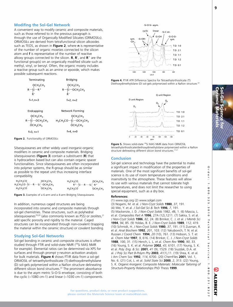
Studying Sol-Gel NetworksSol-gel bonding in ceramic and composite structures is often studied through FTIR and solid-state NMR (29Si MAS NMR for example). Elemental ratios can be determined via XPS for surfaces and through prompt γ neutron activation analysis for bulk materials. Figure � shows FT-IR data from a sol-gel ORMOSIL of tetraethylorthosilicate (T):diethoxydimethylsilane (D) sol-gels polymerized within a Nafion structure delineating different silicon bond structures.22 The prominent absorbance is due to the asym metric Si-O-Si envelope, consisting of both the cyclic (~1080 cm-1) and linear (~1030 cm-1) components.
1400 1200 1000 800 600
cm -1
sym.-CH 3
-Si-OEt
-Si-O-Si- asym.
cyclic linear
-Si-OH
-Si-C str.
-Si-O-Si-sym.
T:D 1:0
T:D 2:1
T:D 1:1
T:D 1:2
T:D 0:1
Figure �. FT-IR ATR Difference Spectra for Tetraethylorthosilicate (T):Diethoxydimethylsilane (D) sol-gels polymerized within a Nafion structure.22
0 - 20 - 40 - 60 - 80 -100 -120 -140
ppm
T:D 1:0
T:D 2:1
T:D 1:1
T:D 1:2
T:D 0:1
D unit Region
Q unit Region
D2
Q4Q3
Figure 5. Shows solid-state 29Si MAS NMR data from ORMOSIL tetraethylorthosilicate/diethoxydimethylsilane polymerized within a Nafion structure delineating different silicon bond structures.17,21
ConclusionSol-gel science and technology have the potential to make a significant impact in modification of the properties of materials. One of the most significant benefits of sol-gel science is its use of room temperature conditions and insensitivity to the atmosphere. These features will allow its use with various materials that cannot tolerate high temperatures, and does not limit the researcher to using special equipment, such as a dry box.
References: (1) www.isgs.org (2) www.solgel.com (3) Nogami, M. et al. J Non-Cryst Solids 1980, 37, 191. (4) Wei, Y. et al. J Sol-Gel Sci & Tech 1996, 7, 191. (5) Mackenzie, J. D. J Non-Cryst Solids 1982, 48, 1. (6) Mascia, L. et al. Composites Part A 1996, 27A (12),1211. (7) Sakka, S. et al. J Non-Cryst Solids 1986, 82, 24. (8) Brinker, C. J. et al. J Memb Sci 199�, 94, 85. (9) Yoldas, B. E. J Non-Cryst Solids 1989, 112, 419. (10) Schmidt, H. J Non-Cryst Solids 1980, 37, 191. (11) Zusman, R. et al. Anal Biochem 199�, 201, 103. (12) Yakubovich, T. N. et al. Russian J Coord Chem 199�, 20 (10), 761. (13) Hobson, S. T. et al. Chem Mat 1997, 9, 616. (14) Brinker, C. J. J Non-Cryst Solids 1988, 100, 31. (15) Hench, L. L. et al. Chem Rev 1990, 90, 33. (16) Young, S. K. et al. Polymer �00�, 43, 6101. (17) Young, S. K. et al. Poly. Eng. & Sci. �001, 41 (9), 1529. (18) Siuzdak, D.A. et al. J Poly Sci Part B-Polym Phy �003, 41(1),11. (19) Shea, K. et al. J Am Chem Soc 199�, 114, 6700. (20) ChemFiles �001, Vol. 1, No. 6. (21) Cot, L. et al. Solid State Sci �000, 2, 313. (22) Young, S. K. Organic-Inorganic Composite Materials: Molecular Tailoring of Structure-Property Relationships PhD Thesis 1999.

TO ORDER: Contact your local Sigma-Aldrich office (see back cover), call 1-800-3�5-3010 (USA), or visit sigma-aldrich.com/matsci.s
ig
ma
-a
ld
ri
ch
.c
om
10So
l-G
el
Sci
en
ce f
or
Cera
mic
Mate
rials
Tri(methoxy)silanes H3CO Si
OCH3
OCH3
R
CH3
��0175 (95%)
CH3CH2
�356�3 (>97%)
CHCH2
�35758 (98%) 10�7�� (98%)
CH2
�383�0 (98%)
CF3CH2
91877 (97%)
OCH2
�133�1 (98%)
CH2 Cl
��0183 (>97%)
CH2 Br 18�65 (97%)
CH2 SH
175617 (95%)
CH2 NH2
�81778 (97%)
CH2 HN CH3
551635 (97%)
CH2 HNNH2
O
��0817 (97%)
CH2 HNNH2
10�88� (97%)
HNCH2
��0809 (97%)
CH2 N H2CCH3
SiOCH3
OCH3
OCH3
555150 (97%)
CH2 OO
��0167 (98%)
CH2 OCH3
H2C
O
��0159 (98%)
CH2(CH2)6CH3
376��1 (96%)
CH2(CH2)14CH3
5�360 (>85%)
CH2(CH2)16CH3
376�13 (90%)
Tri(ethoxy)Silanes H3CH2CO Si
OCH2CH3
OCH2CH3
R
CH2
CH2
3910�� (96%)
CH2
CH3
539317 (97%)CH2
CH3
H3C
�35678 (98%)
CH2 �9�6� (>97%)
CH2
CH2
A36301 (97%)CH2
CN
1�5377 (97%)
CH2(CH2)3CH3
10160 (>97%)Cl
CH2
�35686 (95%)
CH2 NH2
��01�0 (99%)CNCH2
37�156 (98%)
CH2(CH2)6CH3
��0�13 (>96%)
CH2CH2CF2(CF2)4CF3
667��0 (98%)
CH2CH2CF2(CF2)6CF3
658758 (97%)
CH2(CH2)10CH3
���37 (>95%)
Other Alkoxysilanes
H3C SiCH3
OCH3
CH3
�53006 (99%)
H3C SiCH3
OCH2CH3
CH3
�5�371 (98%)
SiCH3
OCH2CH3
OCH2CH3H3C
175595 (97%)
H3C SiOCH3
OCH3
��6�03 (97%)
H3CH2CO SiOCH2CH3
CH3
CH2
�59�6� (99%)
Si
OCH2CH3
�8�319 (97%)
H3C SiOCH3
OCH3
CH2(CH2)6CH3
68�15 (>95%)
H3C SiCH3
OCH3
CH2(CH2)6CH3
375977 (98%)
SiOCH2CH3
OCH2CH3
CH2(CH2)16CH3H3C
�5�793 (95%)
H3CH2CO SiOCH2CH3
CH3
NH2
371890 (97%)
H2CH3CO SiCH3
OCH2CH3
O O
�35171 (97%)
H2CH3CO SiCH3
CH3
O O
539�60 (97%)
H3CO SiCH3
OCH3
SH
��6173 (95%)
H3CH2CO Si
OCH2CH3
D8353� (97%)
Silane PrecursorsFor unit sizes and prices of products below, please visit sigma-aldrich.com.

For questions, product data, or new product suggestions, please contact the Materials Science team at [email protected].
Or
de
r:
1
.8
00
.3
25
.3
01
0
Te
ch
ni
ca
l
Se
rv
ic
e:
1
.8
00
.2
31
.8
32
7
11H
erm
etic B
arrie
r Usin
g
VTE
OS &
So
l-Gel P
roce
ssing
IntroductionHumidity barriers are an essential part of microelectronics, micro-electromechanical systems (MEMS) and displays using organic-light emitting diodes (OLEDs). These barriers are required to have low processing temperatures. Hybrid organic-inorganic barrier materials can be applied in a sol-gel process at low temperature, in order to provide hermeticity. The inorganic content is designed to be the barrier, while the hydrophobic, organic content repels water and fills porosity.
Our goal is to develop hermetic barriers for electronics and electrochemical devices. The barrier has to prevent water, water vapor, and gases from permeating the coating and reacting with the device. Many low temperature hybrids have been synthesized using the sol-gel process and methacrylate compounds.1,2 Other hybrids have been discussed in detail.3,4 The concept is that the sol-gel process produces an oxide at low temperatures. Specifically, the process is used to produce silica, either as a network or as an agglomeration of nano-sized particles. The hybrid approach incorporates an organic component with the oxide, by either simultaneously or sequentially polymerizing the organic along with the inorganic component.
Typically, the inorganic component is derived from the hydrolysis and condensation polymerization of tetraethyl orthosilicate (TEOS, Aldrich Prod. No. 333859) to form a network of silica, containing bridging oxygens. In this study, we use vinyl triethoxysilane (VTEOS, Aldrich Prod. No. 679�75) to generate an oxide network with polymerizable vinyl groups. In this case, the advantage of VTEOS over TEOS is the presence of an inorganic and organic network.
We analyzed the effectiveness of VTEOS in creating a hydrophobic barrier and how ultraviolet (UV) irradiation affected the VTEOS system. The properties of the films were investigated, and contact angle measurements were made to assess hydrophobicity.
Synthesis MethodThe flowchart for synthesizing barrier coatings is shown in Figure 1. First the precursor, vinyl triethoxysilane (VTEOS), was mixed with the solvent ethylene glycol mono-butyl ether (EGMBE). Deionized water and acetic acid (CH3COOH) were added and the solution was stirred for 20 hours. The initiator was benzoyl peroxide (BPO) for free-radical polymerization (0.1 wt %). Once the initiator was added, the solution was stirred for 4 hours before microscope slides and stainless steel coupons were dipped into the solution. A dip coater with a screw drive was used to lower and raise the slide.
The films were allowed to dry over night at room temperature before heating to 70 ºC for 30 minutes. UV irradiation was carried out, followed by a wash in NaOH to remove excess BPO. Finally, the samples were dried and evaluated.
Uniform films were obtained on both glass and stainless steel substrates. Contact angle measurements were acquired using deionized water and calculated using KSV CAM Optical Contact Angle with Pendant Drop Surface Tension Software 3.80. The AFM images were acquired in a contact mode using a Nanoscope IV Scanning probe microscope Veeco™.
Stir 4 hours
VTEOS +EGMBE
Stir 20 hours
Remove excess initiator with NaOH
UV irradiation (10 minutes – 2 hours)
Heat at 70 °C: 30 minutes
Dry at RT overnight
Adding BPO
Dip Coat
Dry overnight at 70 °C
H2O + CH3COOH
Figure 1. Flow chart of the synthesis of hybrid coatings using VTEOS via a sol-gel process.
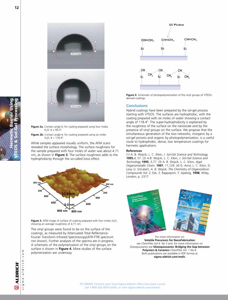
Results and DiscussionTwo samples are compared. One coating was prepared with four moles of water to one mole of VTEOS and the other one with six moles of water to one mole of VTEOS. Four moles is commonly said to be the stoichiometric water to hydrolyze a tetrafunctional silane, making six moles an excess. This assumes that one mole of water hydrolyzes each ethoxy group, although some condensation polymerization often accompanies further hydrolysis.
The results of the contact angle measurement are shown in Figures �a and �b. In Figure 2a, the contact angle for the drop of water on the coating prepared with four moles of water is 90.5º. For the sample that used six moles of water, the measured contact angle is 118.4º. This angle is much greater than 90º, and the coating is clearly super-hydrophobic.
Development of a Hermetic Barrier Using Vinyl Triethoxysilane (VTEOS) and Sol-Gel Processing
Ariel Jackson, and Dr. Andrei Jitianu, Professor Lisa C. Klein
Department of Materials Science and Engineering, Rutgers University
TO ORDER: Contact your local Sigma-Aldrich office (see back cover), call 1-800-3�5-3010 (USA), or visit sigma-aldrich.com/matsci.s
ig
ma
-a
ld
ri
ch
.c
om
1�
Figure �a. Contact angle u, for coating prepared using four moles H2O: u = 90.5°.
Figure �b. Contact angle u, for coating prepared using six moles H2O: u = 118.4°.
While samples appeared visually uniform, the AFM scans revealed the surface morphology. The surface roughness for the sample prepared with four moles of water was about 4.71 nm, as shown in Figure 3. The surface roughness adds to the hydrophobicity through the so-called lotus effect.
800 nm
200
400
600 600
400
200
800 nm
800 nm 800 nm
0.0 nm
50.0 nm
Figure 3. AFM image of surface of coating prepared with four moles H2O, showing an average roughness of 4.71 nm.
The vinyl groups were found to be on the surface of the coatings, as measured by Attenuated Total Reflectance-Fourier Transform Infrared Spectroscopy(ATR-FTIR spectrum not shown). Further analyses of the spectra are in progress. A schematic of the polymerization of the vinyl groups on the surface is shown in Figure �. More studies of the surface polymerization are underway.
Herm
eti
c B
arr
ier
Usi
ng
V
TEO
S &
So
l-G
el
Pro
cess
ing
Figure �. Schematic of photopolymerization of the vinyl groups of VTEOS-derived coatings.
ConclusionsHybrid coatings have been prepared by the sol-gel process starting with VTEOS. The surfaces are hydrophobic, with the coating prepared with six moles of water showing a contact angle of 118.4º. The super-hydrophobicity is explained by the roughness of the surface on the nanoscale and by the presence of vinyl groups on the surface. We propose that the simultaneous generation of the two networks, inorganic by a sol-gel process and organic by photopolymerization, is a useful route to hydrophobic, dense, low temperature coatings for hermetic applications.
References (1) A. B. Wojcik, L. C. Klein, J. Sol-Gel Science and Technology, 1995,4, 57. (2) A.B. Wojcik, L. C. Klein, J. Sol-Gel Science and Technology 1995, 5,77. (3) A. B. Wojcik, L. C. Klein, Appl. Organometallic Chem. 1997, 11,129. (4) D. Avnir, L. C. Klein, D. Levy, U. Schubert, A. B. Wojcik, The Chemistry of Organosilicon Compounds Vol. 2, Eds. Z. Rappoport, Y. Apeloig, 1998, Wiley, London, p. 2317.
For more information on Volatile Precursors for NanoFabrication
see ChemFiles Vol 4. No 3 and, for more information onSilsesquioxanes see Silsesquioxanes: Bridging the Gap between
Polymers & Ceramics ChemFiles Vol. 1 No 6.Both publications are available in PDF format at
sigma-aldrich.com/mslit.

For questions, product data, or new product suggestions, please contact the Materials Science team at [email protected].
Or
de
r:
1
.8
00
.3
25
.3
01
0
Te
ch
ni
ca
l
Se
rv
ic
e:
1
.8
00
.2
31
.8
32
7
13
Deposition Grade Silanes for Sol-Gel Processing
Silane Precursor Structure Product No.
AllyltrimethoxysilaneSiH3COOCH3
OCH3CH2
679�67-50G
Butyltrichlorosilane Cl3Si CH3 679���-50G
[3-(Diethylamino)propyl]trimethoxysilaneSi
OCH3
OCH3
H3CON
CH3
CH3 679356-50G
Ethyltrichlorosilane CH3Cl3Si 679�16-50G
Isobutyl(trimethoxy)silane CH3Cl3Si 67936�-50G
Methyltrichlorosilane CH3Cl3Si 679�08-50G
N-PropyltriethoxysilaneH3CH2CO Si
OCH2CH3
OCH2CH3
CH3
6793�1-50G
Pentyltrichlorosilane Cl3Si CH3 67919�-50G
Tetramethyl orthosilicateH3CO Si
OCH3
OCH3
OCH3
679�59-50G
Tetrapropyl orthosilicateH3CH2CH2CO Si
OCH2CH2CH3
OCH2CH2CH3
OCH2CH2CH3
679��0-50G
Triethoxy(octyl)silaneH3CH2O Si
OCH2CH3
OH2CH3
CH3
679305-50G
TriethoxyphenylsilaneH3CH2CO Si
OCH2CH3
OCH2CH3
679�91-50G
TriethoxyvinylsilaneH3CH2CO Si
OCH2CH3
OCH2CH3
CH2
679�75-50G
TrimethoxymethylsilaneH3CO Si
OCH3
OCH3
CH3
679�3�-50G
TrimethoxyphenylsilaneSiH3CO
OCH3
OCH3
679313-50G
Purity of the above deposition-grade silanes is 98+% by chemical assay. Trace metals and impurity profiles are reported on the Certificate of Analysis.
For a complete list of precursors for Sol-Gel Processing, visit sigma-aldrich.com/solgel.
Herm
etic B
arrie
r Usin
g
VTE
OS &
So
l-Gel P
roce
ssing
TO ORDER: Contact your local Sigma-Aldrich office (see back cover), call 1-800-3�5-3010 (USA), or visit sigma-aldrich.com/matsci.s
ig
ma
-a
ld
ri
ch
.c
om
1�
In the past decade, the integration of passive components in silicon and the further 3D integration and stacking of individual chips from different technologies (e.g. CMOS, GaAs, MEMS) into one package (‘heterogeneous’ integration) have been developed to such an extent that now the first mass-volume production has begun. Today, the International Technology Roadmap for Semiconductors includes the future projections for the next generation Si-based Integrated Passives and System-in-Package integration.1
Recently, the first highly-integrated cellular RF transceiver systems based on the use of these technologies were launched.2 Here, amongst others, Philips (now NXP) Semiconductors, utilizes back-end silicon processing to integrate passive components onto a silicon substrate that can act as a carrier for the heterogeneous integration of active component dies, MEMS dies, etc.3 As an example, a transceiver IC can be flip-chip mounted onto this passive component silicon substrate, thus minimizing interconnect parasitics and the footprint area. This sub-assembly is then flipped back into a standard leadframe package (Figure 1).3
transceiver die150 µm thick
passive die300 µm thick
lead frame
flip
flipflip
Decoupling and PLL capacitors
transceiver
flip
flipflip
flip
flipflipflip
transceiver
Figure 1. Passive die with active transceiver die flipped on top, double-flipped on a lead frame (left open, without moulding compound). This is an example of a Bluetooth System-in-Package ‘plug and play’ radio module. (From Ref. 3).
The passive die is made in the so-called PICS (Passive Integration Connecting Substrate) technology developed to integrate passive components such as high-Q inductors, resistors, accurate MIM capacitors and, in particular, high-density (~30 nF/mm2) MOS ‘trench’ capacitors for decoupling and filtering. These are fabricated in silicon by dry-etching arrays of macropores with ~1.5 µm width and up to ~30 µm depth. Trench capacitors filled with ~ 30 nm silicon oxide and nitride (‘ONO’) dielectrics and a poly-Si/ Al top electrode showed superior dielectric breakdown voltage (30 V typical), very low leakage current, and long lifetime.4,5
Sil
ico
n-B
ase
d P
ass
ive a
nd
Syst
em
-in
-Pack
ag
e
Silicon-Based Passive and System-in-Package Integration: Options for Atomic Layer Deposition
A next miniaturization step includes the use of so-called high-k dielectrics (based on HfO2, etc.) to compose MIS and MIM trench capacitors with increased capacitance densities of ≥200 nF/mm2. One step towards System-in-Package is the etching and Cu-filling (electroplating) of viaholes of 10–200 µm widths and depths up to 300 µm. Vias are through-wafer holes filled with materials for heat spreading, electrical grounding and low-inductance signal interconnection from one wafer side to the other. This concept makes way for 3D die-stacking and generic System-in-Package integration with small form factor.
One of the major challenges in realizing high-density trench capacitors and in making through-wafer vias for 3D wafer and die stacking is to find an attractive pore lining and filling fabrication technology at reasonable cost and reaction rate as well as low temperature (for back-end processing freedom). The deposition for the insulating, dielectric, and performed at conductive layers (i.e. electrodes, seed layers and Cu-diffusion barriers) should be highly uniform and step-conformal and low-temperature (≤400 °C). Atomic Layer Deposition (ALD) is an enabling candidate here, by virtue of the self-limiting mechanism of this layer-by-layer deposition technique. A substrate surface is submitted to alternating exposures to vapors of two reagents, for example, trimethylaluminum (TMA) and water vapor in the case of Al2O3 deposition. Through its self-limiting surface reactions, ALD enables the uniform lining or filling of high aspect ratio pores with (sub)monolayer control. The self-limiting character provides inherent conformality, as demonstrated for even challenging devices like deep DRAM trench capacitors with ~60:1 aspect ratios at design rules below 100 nm.6 Yet, ALD process improves the production of many other devices with a large topology, such as viaholes in stacked dies, MEMS, planar waveguides, multilayer optical filters, and layers protecting against diffusion, oxidation, corrosion, etc.
The application of ALD in trench capacitors and viaholes leads to additional challenges relative to flat wafers. For example, for the ALD of oxides the roughness on the trench sidewalls may cause undesired lower breakdown voltages. Also, the formation of interfacial oxide layers may lead to undesired low relative dielectric constants (cf. Figure �). A proper pre-cleaning procedure (e.g. HF dipping, rinsing) is essential to minimize this. Furthermore, a proper uniform layer thickness and microstructure (morphology and texture) over the entire pore depth is necessary to achieve good insulating layers, and are certainly not obvious. Adsorption and desorption play an important role in filling and emptying the pores. In particular, at the given pressure and macropore dimensions the ALD process proceeds in a different diffusion regime (Knudsen diffusion) limiting the free diffusion of the gaseous ALD reagents and products. Timing of the cycling of the gases, including extended purging steps, needs to be optimized for additional adsorption and desorption processes of precursors.7 Only then ideal nanolaminates can be achieved.
Dr. Fred Roozeboom, NXP Semiconductors Research and Dr. Erwin Kessels, University of Technology, Eindhoven

For questions, product data, or new product suggestions, please contact the Materials Science team at [email protected].
Or
de
r:
1
.8
00
.3
25
.3
01
0
Te
ch
ni
ca
l
Se
rv
ic
e:
1
.8
00
.2
31
.8
32
7
15Silico
n-B
ase
d P
assiv
e a
nd
Syste
m-in
-Pack
ag
e
For the deposition of conductive layers by ALD, for the application as electrodes, seed layers, diffusion barriers (e.g. against Cu-diffusion in vias) there is a substantial choice between thermal and plasma-assisted ALD. The plasma-based process can lead to improved material properties as has clearly been demonstrated by results on conductive TiN films.8 The process based on TiCl4 dosing in combination with H2-N2 plasma exposure has yielded thin TiN films with excellent resistivity and low impurity levels (C, H, Cl, etc.) greatly surpassing the material quality achieved with the thermal process employing NH3 dosing. Moreover, in terms of acceptable material quality, the thermal process is limited to the substrate temperature range of 300–400 °C while the plasma-based process can yield fair material properties down to temperatures as low as 100 °C.
M
I
S
polySi
Al 2 O 3 /HfO 2 /Al 2 O 3
a b
interfacial SiO2
poly-Si
Al2O3
HfO2
Al2O3
SiO2
Si-substrate
0.5 µm 10 nm
Figure �. (a) SEM cross-section and (b) high-resolution TEM image of an Al2O3/HfO2/Al2O3 dielectric layer stack, grown by thermal ALD with a poly-Si electrode layer on top.
TiN films deposited by plasma-assisted ALD for application as electrode materials in trench capacitors have already been explored (Figure 3). Another benefit from the plasma process is that tailoring the plasma composition and exposure time as shown for metal nitrides such as TiN and TaN can control the stoichiometry of the films. For example, for TaN deposited from metalorganic precursors (e.g., pentakisdimethyl aminotantalum) it is possible to tune the properties from insulating N-rich TaN by using a H2-N2 plasma, to low-resistivity TaN by using a relatively long H2 plasma exposure, to very low resisitivity TaCN films with a large amount of carbon using a relatively short H2 plasma exposure.
100 nm
TiNONO
Sipoly-Si
100 nm
TiNONO
Sipoly-Si
b
SiSiO2
Si3N4
SiO2
TiN
poly -Si
10 nm
30 nm ONO
a b
Figure 3. (a) SEM cross-section and (b) high-resolution TEM image of a MOS stack consisting of 30 nm ‘ONO’ dielectric and 10 nm plasma-assisted ALD TiN with 0.3 µm LPCVD grown poly-Si on top.
ALD is, in principle, ideal for depositing nanolaminate stacks, for example oxide/nitride multilayers used in trench capacitors. Multilayer stacks of ‘high-k’ dielectric layers (Al2O3, Ta2O5, HfO2, etc.) and conductive layers (TiN, TaN) on wafers with a large topography enable MIM capacitors with ultrahigh capacitance density. A challenging example is given in Figure �. The TEM images show the potential of ALD in growing multilayer stacks in high aspect ratio features. In our macropore arrays described above, a multilayer stack of 20 nm Al2O3 // 25 nm TiN // 20 nm Al2O3 // 25 nm TiN was deposited in 35 µm deep pores from TiCl4 and NH3 using thermal ALD. Here, the Al2O3 was grown from trimethylaluminum and O3 plasma at 380 °C and the TiN was grown from TiCl4 and NH3 at 400 °C. It appeared that the layer thickness all along the pores was, within 10 % accuracy, 20 nm for the Al2O3 and 25 nm for TiN.
AI2O3
TiNAI2O3
Si
Silica residues(from polishing)
(a) (b)
(c) (d)
100 nm
0.5 µm 50 nm
50 nm
Figure �. TEM images of a 20 nm Al2O3 // 25 nm TiN // 20 nm Al2O3 // 25 nm TiN multilayer grown in a pore with ~35 µm depth; a) overview image displaying both sides of one pore (top); b) and c) images at the upper part of the pore; d) image at ~25 µm pore depth. ALD performed by H.D. Kim, Jusung Engineering.
It can be concluded that the manufacturing of ultrahigh density (>200 nF/mm2) capacitors is within reach and the same holds for growing seed layers for Cu-electroplating in viaholes and Cu-diffusion layers such as TaN. Thus there is a bright prospect for ALD in passive and heterogeneous integration, provided ALD is further developed to maturity and cost factors are reduced (e.g. development of batch ALD to compensate for low growth rates in single-wafer ALD). Also the development of low-temperature processing is important. This will be further facilitated by the availability of novel and dedicated precursor chemicals.

TO ORDER: Contact your local Sigma-Aldrich office (see back cover), call 1-800-3�5-3010 (USA), or visit sigma-aldrich.com/matsci.s
ig
ma
-a
ld
ri
ch
.c
om
16
AcknowledgementThe technical contributions by J. Klootwijk, W. Dekkers and M. Kaiser (Philips) and S. Heil (TU Eindhoven) are gratefully acknowledged.
References(1) ITRS Roadmap �005 edition, Assembly and Packaging, see: www.itrs.net/Links/2005ITRS/Home2005.htm.(2) www.3d-ic.org/literature.html. (3) F. Roozeboom, A.L.A.M. Kemmeren, J.F.C. Verhoeven, F.C. van den Heuvel, J. Klootwijk, H. Kretschman, T. Frič, E.C.E. van Grunsven, S. Bardy, C. Bunel, D. Chevrie, F. LeCornec, S. Ledain, F. Murray and P. Philippe, Thin Solid Films �006, 504, 391. (4) F.Roozeboom, A.Kemmeren, J.Verhoeven, F.van den Heuvel, H.Kretschman and T.Frič, Mat. Res. Soc. Symp. Proc. �003, 783, 157. (5) F. Roozeboom, A.L.A.M.
Kemmeren, J.F.C. Verhoeven, F.C. van den Heuvel, J. Klootwijk, H. Kretschman, T. Frič, E.C.E. van Grunsven, S. Bardy, C. Bunel, D. Chevrie, F. LeCornec, S. Ledain, F. Murray and P. Philippe, Electrochem. Soc. Symp. Proc. �005, 2005,16.(6) M. Gutsche, H. Seidl, J. Luetzen, A. Birner, T. Hecht, S. Jakschik, M. Kerber, M. Leonhardt, P.Moll, T.Pompl, H.Reisinger, S. Rongen, A. Saenger, U. Schroeder, B. Sell, A. Wahl and D. Schumann, Tech. Digest IEDM �001, 18.6 (7) J. Klootwijk, A. Kemmeren, R. Wolters, F. Roozeboom, J. Verhoeven, E. van den Heuvel, in ‘Defects in Advanced High-k Dielectric Nano-Electronic Semiconductor Devices’, (E. Gusev, ed.); Springer: Dordrecht, �006, p. 17. (8) S.B.S. Heil, E. Langereis, F. Roozeboom, M.C.M. van de Sanden and W.M.M. Kessels, J. Electrochem. Soc. �006, 153, G956-G965.
Additional Volatile Precursors for Chemical Vapor and Atomic Layer Deposition
Metal Volatile Precursor Linear FormulaPhysical State/ Handling Precautions
Purity % Product No.
Aluminum Diethylaluminum ethoxide (C2H5)2AlOC2H5 Liquid, pyrophoric 97 �567�9-100G
Trimethylaluminum [TMA]
Al(CH3)3 Liquid, pyrophoric 97 �57���-100G
Tris(dimethylamido)aluminum(III) Al(N(CH3)2)3 Solid, air/moisture -sensitive >98 �699�7-10G
HafniumTetrakis(diethylamidohafnium(IV) [TDEAT]
Hf[N(CH2CH3)2]4 Liquid, air/moisture -sensitive 99.99�55�0�-10G�55�0�-�5G�55�0�-100G
Tetrakis(dimethylamido)hafnium(IV) [TDMAH]
Hf[N(CH3)2]4 Solid, air/moisture -sensitive 99.99�55199-5G�55199-�5G
Tetrakis(ethylmethylamido)hafnium(IV) Hf[N(CH3)C2H5)]4 Liquid, air/moisture -sensitive 99.995531�3-5ML5531�3-�5ML
Tantalum Tris(diethylamido)(ethylimido)tantalm(V) C2H5N=Ta(N(C2H5)2)3 Liquid, air/moisture -sensitive 99.99 517836-5ML
Tris(diethylamido)(tert-butylimido)- tantalum(V)
(CH3)3CN=Ta(N(C2H5)2)3 Liquid, air/moisture -sensitive 99.99 5�1�80-5ML
Tris(ethylmethylamido) (tert-butylimido)tantalum(V)
(CH3)3CN=Ta(N(C2H5)CH3)3 Liquid, air/moisture -sensitive 99.99 J1000�3-5G
TitaniumBis(diethylamido)bis- (dimethylamido)titanium(IV)
Ti(N(CH3)2)2(N(CH2CH3)2)2 Liquid, air/moisture -sensitive 99.99 J1000�6-10G
Titanium(IV) chloride [TICL]
TiCl4 Liquid, air/moisture -sensitive 99.995�5�31�-10G�5�31�-�5G
Tetrakis(diethylamido)titanium(IV) [TDEAT]
Ti[N(C2H5)2]4 Liquid, air/moisture -sensitive 99.999�69866-5G �69866-�5G
Tetrakis(dimethylamido)titanium(IV) [TDMAT]
Ti[N(CH3)2]4 Liquid, air/moisture -sensitive 99.999�69858-5G �69858-�5G
Tetrakis(ethylmethylamido)titanium(IV) [TEMAT]
Ti(N(C2H5)CH3)4 Liquid, air/moisture -sensitive 99.99�73537-5G�73537-�5G
For a complete list of metal precursors for CVD/ALD, visit sigma-aldrich.com/precursors.
Sil
ico
n-B
ase
d P
ass
ive a
nd
Syst
em
-in
-Pack
ag
e

For questions, product data, or new product suggestions, please contact the Materials Science team at [email protected].
Or
de
r:
1
.8
00
.3
25
.3
01
0
Te
ch
ni
ca
l
Se
rv
ic
e:
1
.8
00
.2
31
.8
32
7
17
Dr. David G. O’Neill, Dr. Radoslav Atanasoski (pictured) Alison K. Schmoeckel, Alison K. Schmoeckel, George D. Vernstrom, Dennis P. O’Brien, Dr. Manish Jain, Dr. Thomas E. Wood, The 3M Company
Current PEM fuel cell technology uses platinum as a catalyst. A large body of work seeking to find a Pt replacement involves Oxygen Reduction Reaction (ORR) catalysts produced using nitrogen coordinated transition metal compounds, such as Fe porphyrins or Fe phthalocyanine.1,2,3 Traditionally, these catalysts are made by pyrolyzing transition metal compounds dried onto carbon support particles at temperatures up to 950 ºC in reducing and/or nitrogen-containing atmosphere. Unfortunately, ORR activity of these catalysts has not been enough and attempts to increase the oxygen activity, for example by increasing the Fe content, have not been successful.4 Analytical work by Dodelet’s group, including TOF-SIMS, XPS and other techniques, led to their proposal that a pyridinic structure is required for good oxygen activity.5,6
Figure 1. Structure proposed by Dodelet’s group6 for the species required for ORR catalytic activity.
A new, alternative process to make non-precious ORR metal catalysts for the oxygen reduction reaction is to use vacuum deposition techniques to combine the three elements believed to be required (a transition metal, carbon, and nitrogen).7,8 Processes including pulsed arc plasma deposition, sputter deposition, evaporation and combinations thereof have been used to produce a variety of materials whose catalytic activity was determined by assembling and measuring the oxygen generated electrical current in 50 cm2 fuel cells. The pulsed arc process is well suited to deposit carbon/Fe based catalysts because it can produce a carbon/iron plasma by erosion of a high-purity graphite cathode containing Fe wires.9 The plan is to vary deposition processes and conditions over a wide range while checking their catalytic activity in a 50 cm2 test fuel cell fixture.10,11 However, solely relying on fuel cell testing does not provide clues to process changes that would be most beneficial, but an analytical technique has not been identified that uniquely qualifies catalytic behavior. Nevertheless, an ability to measure a material characteristic that is known to relate to ORR catalysis would significantly improve process R&D.
Therefore, we began using local, element-specific, analytical probes that have the ability to differentiate between Fe-based catalyst materials that have had different process histories but similar compositions. Vacuum deposited C-Nx:Fe catalysts were analyzed using Extended X-ray Absoption Fine Structure (EXAFS) analyses of the Fe k-edge and resonant ultraviolet photoelectron spectroscopy (UPS) to measure the valence electronic structure around Fe atoms. Both techniques show significant differences between samples that received and those that did not, receive thermal treatment.
Results Carbon-nitrogen-iron coatings were deposited onto either a carbon non-woven cloth or Si wafers, depending on the analytical technique to be used, and processed either with or without a thermal treatment. Surface composition measurements by XPS showed that the nitrogen and iron content could be varied between 1–5 at. % for nitrogen and between 0.1 to 7 at. % for iron. This range is much larger than can be obtained with molecular pyrolysis methods (2–3 at. % nitrogen and 0.05 at. % Fe). Analysis of the Fe core level indicates that the iron in these coatings is neither metallic nor an oxide; however some carbide phase cannot be ruled out. High resolution XPS shows that the N 1S core level in vapor deposited C-Nx:Fe coatings has the same doublet structure with a component at 398.5 eV, identified as pyridinic nitrogen, that has been reported for pyrolyzed Fe-derived catalyst materials.6 The fact that the nitrogen exhibits the same XPS fingerprint as pyrolyzed Fe catalysts combined with the fact that the nitrogen and iron content is much higher than in pyrolyzed Fe catalysts suggested that the catalytic currents would be higher. However, our electrochemical fuel cell testing showed the opposite to be true. Although a direct comparison is difficult, after correcting for large differences in surface area, the ORR catalytic activity of vapor deposited coatings is lower than that of pyrolyzed Fe catalysts. Although a thermal treatment above 650 °C, either during or after deposition, significantly increased catalytic activity the level was still below that of pyrolyzed molecular compounds.
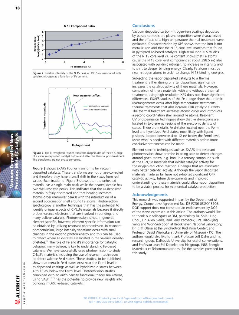
The similarity of vacuum deposited coatings based on XPS spectra and the difference in their electrochemical behavior suggests that more detailed materials characterization is needed. Detailed analyses of the N 1S core-level shows that the intensity and binding energy of the 398.5 eV component, the component normally associated with pyridinic nitrogen, changes with iron content. For example, in C-Nx:Fe(7 at. %) the intensity is 75% of the total N 1S intensity, whereas in a nitrogenated carbon (i.e. without iron) the intensity is only 45% of the total. Indeed, the pyridinic component intensity steadily increases as the Fe content increases, as shown by the graph in Figure �. In addition, the pyridinic components binding energy increases with increasing iron content. The shift to deeper binding energy is similar to findings by Dodelet’s group for pyrolyzed Fe-derived catalysts, although in those materials the shift is much less.6 The fact that a small amount of iron has such an effect on the nitrogen core level binding energy suggests that Fe and N atoms are near each other instead of being uniformly dispersed.
Vacuum Deposited Non-Precious Metal Catalysts for PEM Fuel Cells
Vacu
um
Dep
osite
d N
on
-Pre
ciou
s Meta
l Cata
lysts
TO ORDER: Contact your local Sigma-Aldrich office (see back cover), call 1-800-3�5-3010 (USA), or visit sigma-aldrich.com/matsci.s
ig
ma
-a
ld
ri
ch
.c
om
18V
acu
um
Dep
osi
ted
No
n-
Pre
cio
us
Meta
l C
ata
lyst
s
N 1S Component Ratio
0
1
2
3
4
5
6
0 2 4 6 8
Fe content (at %)
Rat
io (
398e
V
Pea
k)/(
400e
V P
eak)
Figure �. Relative intensity of the N 1S peak at 398.5 eV associated with pyridinic nitrogen as a function of Fe content.
Heat treatment effect
Tran
sfo
rm m
agn
itu
de
R (Angstroms)
2 4
Without heat treatment
After heat treatment
Figure 3. The k3-weighted Fourier transform magnitudes of the Fe K-edge of a vacuum deposited catalyst before and after the thermal post-treatment. The transforms are not phase-corrected.
Figure 3 shows EXAFS Fourier transforms for vacuum deposited catalysts. These transforms are not phase-corrected and therefore they have a small shift in the x-axis from real values. Examination of Figure 3 shows that the unheated material has a single main peak while the heated sample has two well-resolved peaks. This indicates that the as-deposited material is fairly disordered and that heating increases atomic order (narrower peaks) with the introduction of a second coordination shell around Fe atoms. Photoelectron spectroscopy is another technique that has the potential to identify unique aspects of C-Nx:Fe materials because it directly probes valence electrons that are involved in bonding, and many believe catalysis. Photoemission is not, in general, element specific, however, element specific information can be obtained by utilizing resonant photoemission. In resonant photoemission, large intensity variations occur with small changes in the exciting photon energy and this can be used to detect where Fe d-states are located in the valence density-of-states.12 The role of Fe and it’s importance for catalytic behavior, many believe, is key to understanding Fe-based catalysts. We have successfully used photoemission to study C-Nx:Fe materials including the use of resonant techniques to detect valence Fe d-states. These studies, to be published, show that metallic Fe d-states exist near the Fermi level in as-deposited coatings as well as hybridized d-states between 4 to 10 eV below the Fermi level. Photoemission studies combined with ab initio density functional theory simulations, using VASP,12,13 has the potential to provide new insights into bonding in ORR Fe-based catalysts.
ConclusionsVacuum deposited carbon-nitrogen-iron coatings deposited by pulsed cathodic arc plasma deposition were characterized and the effects of a high temperature thermal treatment were evaluated. Characterization by XPS shows that the iron is not metallic iron and that the N 1S core level matches that found in pyrolyzed Fe-based catalysts. High resolution XPS studies of the N 1S core level vs. Fe content shows that Fe atoms cause the N 1S core level component at about 398.5 eV, also associated with pyridinic nitrogen, to increase in intensity and to shift to deeper binding energy. Clearly, Fe atoms must be near nitrogen atoms in order to change N 1S binding energies.
Subjecting the vapor deposited catalysts to a thermal treatment, either during or after deposition, significantly increases the catalytic activity of these materials. However, comparison of these materials, with and without a thermal treatment, using high resolution XPS does not show significant differences. EXAFS studies of the Fe k-edge show that atomic rearrangements occur after high temperature treatments, thermal treatments that also increase ORR catalytic currents. The thermal treatment increases atomic order and introduces a second coordination shell around Fe atoms. Resonant UV photoemission techniques show that Fe d-electrons are located in two energy regions of the electronic density of states. There are metallic Fe d-states located near the Fermi level and hybridized Fe d-states, most likely with ligand p-states, located between 4 to 12 eV below the Fermi level. More work is needed with different materials before more conclusive statements can be made.
Element specific techniques such as EXAFS and resonant photoemission show promise in being able to detect changes around given atoms, e.g. iron, in a ternary compound such as the C-Nx:Fe materials that exhibit catalytic activity for the oxygen-reduction reaction. Changes that are associated with better catalytic activity. Although the vapor deposited materials made so far have not exhibited significant ORR catalytic activity, future developments and improved understanding of these materials could allow vapor deposition to be a viable process for economical catalyst production.
AcknowledgmentsThis research was supported in part by the Department of Energy, Cooperative Agreement No. DE-FC36-03GO13106. DOE support does not constitute an endorsement by DOE of the views expressed in this article. The authors would like to thank our colleagues at 3M, particularly Dr. Shih-Hung Chou, Dr. Allen Siedle, and Terry Pechacek; Drs. Xiao-Qing Yang and Won-Sub Soon at Brookhaven National Laboratory; Dr. Cliff Olson at the Synchrotron Radiation Center; and Professor David Wieliczka at University of Missouri - KC. The authors would also like to thank Professor Jeff Dahn and his research group, Dalhousie University, for useful conversations, and Professor Jean-Pol Dodelet and his group, INRS-Energie, Materiaux et Telcommunications, for the samples provided for this study.

For questions, product data, or new product suggestions, please contact the Materials Science team at [email protected].
Or
de
r:
1
.8
00
.3
25
.3
01
0
Te
ch
ni
ca
l
Se
rv
ic
e:
1
.8
00
.2
31
.8
32
7
19
References and Note(1) Terminology Convention: “pyrolyzed, Fe-derived” will refer to the catalyst syntheses using Fe containing molecules, such as Fe porphoryns, Fe phthalocyanines, Fe-acetate, etc. (2) N4-Macrocyclic Metal Complexes: Electrocatalysis, Electrophotochemistry & Biomimetic Electroanalysis. Edited by J. Zagal, F. Bedioui, and J. P. Dodelet, Springer �006. (3) H. A. Gasteiger, S. S. Kocha, B. Sompalli, F. T. Wagner, Applied Cat. B: Environ., �005, 9, 56. (4) J.-P. Dodelet in N4-Macrocyclic Metal Complexes: Electrocatalysis, Electrophotochemistry & Biomimetic Electroanalysis. Edited by J. Zagal, F. Bedioui, and J. P. Dodelet, Springer �006. (5) F. Jaouen, M. Lefevre, J.-P. Dodelet, and M. Cai, J. Phys. Chem. B, �006, 5553, 110. (6) F. Jaouen, S. Marcott, J.-P. Dodelet and G. Lindbergh, J. Phys. Chem. B, �003, 1376, 107. (7) R.T. Atanasoski, Novel Approach to Non-Precious Metal Catalysts, DOE Hydrogen Program FY �00� Progress Report (V.C.5).
(8) G. Lalande, D. Guay, J. P. Dodelet, S. A. Majetich, M.E.McHenry, Chem. Mater., 1997, 784, 9. E. Bradley Easton, Arman Bonakdarpour, and J.R. Dahn, Electrochem. and Solid-State Lett., �006, A463, 9. (9) E.I. Tochitsky, O.V. Selifanov, V.V. Akulich, I.A. Kapustin and A.V. Stanishevskii, Surface and Coatings Technology, 1991 522, 47. (10) R.T. Atanasoski, Novel Approach to Non-Precious Metal Catalysts, DOE Hydrogen Program FY �005 Progress Report (V.C.5). (11) R.T. Atanasoski, Novel Approach to Non-Precious Metal Catalysts, DOE Hydrogen Program FY �006 Progress Report. (12) G. Kresse and J. Hafner, Phys. Rev. B, �7, 558 (1993); G. Kresse and J. Furthmüller, Phys. Rev. B, 1996, 11169, 54. G. Kresse and J. Furthmüller, Comput. Mater. Sci., 1996, 15, 6. G. Kresse and D. Joubert, Phys. Rev. B, 1999, 1758, 59. (13) M. Jain, S.-H. Chou, A. Siedle, J. Phys. Chem. B, �006, 4179, 110.
High-Purity Graphite and Iron
Materials Physical Form Size/density Purity (%) Product No.
Iron Wire diam. 0.5 mm 99.99 �66��8-7.5G
diam. 1.0 mm 99.99�66�56-3.1G �66�56-15.5G
diam. 0.5 mm 99.935683�-1.5G 35683�-7.5G
diam. 1.0 mm 99.93568��-6.�G3568��-31G
Foil thickness 0.25 mm 99.993381�1-1.�G 3381�1-5G
thickness 0.1 mm 99.9356808-�G356808-8G
Granule 10–40 mesh 99.999�1305�-5G�1305�-�5G
Rod diam. 6.3 mm 99.98�66�13-30G�66�13-150G
Graphite Rod length 150 mm, diam. 3 mm, low density 99.999 �96537-�3.5G
length 150 mm, diam. 3 mm, high density 99.995 �965�5-60G
length 150 mm, diam. 6 mm, low density 99.999 �96553-180.7G
length 150 mm, diam. 6 mm, high density 99.995 �96561-��0.5G
Safe and Simple• Gas dispensing and storage in one compact, portable system• Keeps lecture-bottles upright and stable, eliminates tip-over• Reduces equipment damage and chance of personal injury• Choice of four models matched to the application• Wall-mountable• Express Service™ Program for fast cleaning, repair, or component replacement
Order Information
Description Prod. No. Non-Corrosive Lecture-Bottle Station Z56�599-1EA 825.00
High-Purity Lecture-Bottle Station Z56�60�-1EA 995.00
Lecture-Bottle Station with T-Purge Valve Z56�610-1EA 1,350.00
Corrosive Lecture-Bottle Station with Cross-Purge Valve Z56�6�9-1EA 2,625.00
Lecture-Bottle Service Station Z56�637-1EA 460.00
Visit our Web site for a brochure with complete information about these new Lecture-Bottle dispensing stations, including a Station Selection Guide that matches the correct station to the gas you are using.
sigma-aldrich.com/gases
SIGMA-ALDRICH LECTURE-BOTTLE STATIONS Safe and Simple Systems for Dispensing Lecture-Bottle Gases
Dispensing lecture-bottle gases has never been safer or simpler using these portable lecture-bottle stations. The premium quality components housed within a station are matched to the application, fully assembled, leak-tested, and ready for use. Just connect the station to the lecture-bottle, process, and a source of inert gas if using a station with a purge valve, and you are ready to go.
Vacu
um
Dep
osite
d N
on
-Pre
ciou
s Meta
l Cata
lysts
Accelerating Customers’ Success
through Leadership in Life Science,
High Technology and Service
ArgentinaSIGMA-ALDRICHDEARGENTINA,S.A.Tel:541145561472Fax:541145521698
AustraliaSIGMA-ALDRICHPTy.,LIMITEDFreeTel:1800800097FreeFax:1800800096Tel:61298410555Fax:61298410500
AustriaSIGMA-ALDRICHHANDELSGmbHTel:4316058110Fax:4316058120
BelgiumSIGMA-ALDRICHNV/SA.FreeTel:0800-14747FreeFax:0800-14745Tel:038991301Fax:038991311
BrazilSIGMA-ALDRICHBRASILLTDA.Tel:55113732-3100Fax:55113733-5151
CanadaSIGMA-ALDRICHCANADALTD.FreeTel:800-565-1400FreeFax:800-265-3858Tel:905-829-9500Fax:905-829-9292
ChinaSIGMA-ALDRICH(SHANGHAI)TRADINGCo.LTD.Tel:+86-21-61415566Fax:+86-21-61415567
Czech RepublicSIGMA-ALDRICHS.R.o.Tel:+420246003200Fax:+420246003291
DenmarkSIGMA-ALDRICHDENMARkA/STel:43565910Fax:43565905
FinlandSIGMA-ALDRICHFINLANDTel:(09)3509250Fax:(09)35092555
FranceSIGMA-ALDRICHCHIMIES.à.r.l.Telappelgratuit:0800211408Faxappelgratuit:0800031052
GermanySIGMA-ALDRICHCHEMIEGmbHFreeTel:0800-5155000FreeFax:0800-6490000
GreeceSIGMA-ALDRICH(o.M.)LTDTel:302109948010Fax:302109943831
HungarySIGMA-ALDRICHkftTel:06-1-235-9054Fax:06-1-269-6470Ingyeneszöldtelefon:06-80-355-355Ingyeneszöldfax:06-80-344-344
IndiaSIGMA-ALDRICHCHEMICALSPRIVATELIMITEDTelephoneBangalore:91-80-6621-9600NewDelhi:91-11-4165-4255Mumbai:91-22-2570-2364Hyderabad:91-40-6684-5488FaxBangalore:91-80-6621-9650NewDelhi:91-11-4165-4266Mumbai:91-22-2579-7589Hyderabad:91-40-6684-5466
IrelandSIGMA-ALDRICHIRELANDLTD.FreeTel:1800200888FreeFax:1800600222Tel:35314041900Fax:35314041910
IsraelSIGMA-ALDRICHISRAELLTD.FreeTel:1-800-70-2222Tel:08-948-4100Fax:08-948-4200
ItalySIGMA-ALDRICHS.r.l.Telefono:0233417310Fax:0238010737NumeroVerde:800-827018
JapanSIGMA-ALDRICHJAPANk.k.TokyoTel:0357967300TokyoFax:0357967315
KoreaSIGMA-ALDRICHkoREATel:031-329-9000Fax:031-329-9090
MalaysiaSIGMA-ALDRICH(M)SDN.BHDTel:603-56353321Fax:603-56354116
MexicoSIGMA-ALDRICHQUÍMICA,S.A.deC.V.FreeTel:01-800-007-5300FreeFax:01-800-712-9920
The NetherlandsSIGMA-ALDRICHCHEMIEBVTelGratis:0800-0229088FaxGratis:0800-0229089Tel:078-6205411Fax:078-6205421
New ZealandSIGMA-ALDRICHPTy.,LIMITEDFreeTel:0800936666FreeFax:0800937777Tel:61298410500Fax:61298410500
NorwaySIGMA-ALDRICHNoRWAyASTel:23176060Fax:23176050
PolandSIGMA-ALDRICHSp.zo.o.Tel:0618290100Fax:0618290120
PortugalSIGMA-ALDRICHQUÍMICA,S.A.FreeTel:800202180FreeFax:800202178Tel:219242555Fax:219242610
RussiaSIGMA-ALDRICHRUS,LLCTel:+7(495)621-5828/5923/6037Fax:+7(495)621-5828/5923/6037
SingaporeSIGMA-ALDRICHPTE.LTD.Tel:65-67791200Fax:65-67791822
South AfricaSIGMA-ALDRICHSoUTHAFRICA(PTy)LTD.FreeTel:0800110075FreeFax:0800110079Tel:27119791188Fax:27119791119
SpainSIGMA-ALDRICHQUÍMICA,S.A.FreeTel:900101376FreeFax:900102028Tel:916619977Fax:916619642
SwedenSIGMA-ALDRICHSWEDENABTel:020-350510Fax:020-352522outsideSwedenTel:+4687424200outsideSwedenFax:+4687424243
SwitzerlandSIGMA-ALDRICHCHEMIEGmbHSwissFreeCall:0800800080Tel:+41817552828Fax:+41817552815
United KingdomSIGMA-ALDRICHCoMPANyLTD.FreeTel:0800717181FreeFax:0800378785Tel:01747833000Fax:01747833313SAFC(Uk):01202712305
United StatesSIGMA-ALDRICHP.o.Box14508St.Louis,Missouri63178Toll-Free:(800)325-3010CallCollect:(314)771-5750Toll-FreeFax:(800)325-5052Tel:(314)771-5765Fax:(314)771-5757
Internet sigma-aldrich.com
JCU01671-503403
0116
The SigMA-ALdriCh group
World Headquarters3050 Spruce St., St. Louis, MO 63103(314) 771-5765sigma-aldrich.com
Order/Customer Service (800) 325-3010 • Fax (800) 325-5052
Technical Service (800) 325-5832 • sigma-aldrich.com/techservice
Development/Bulk Manufacturing Inquiries (800) 244-1173
©2006 Sigma-Aldrich Co. All rights reserved.SIGMA, -, SAFC, , SIGMA-ALDRICH, ), ISOTEC, ALDRICH, ^, FLUKA, T, and SUPELCO are trademarks belonging to Sigma-Aldrich Co. and its affiliate Sigma-Aldrich Biotechnology, L.P. Riedel-de Haën® trademark under license from Riedel-de Haën GmbH. Sigma brand products are sold through Sigma-Aldrich, Inc. Sigma-Aldrich, Inc. warrants that its products conform to the information contained in this and other Sigma-Aldrich publications. Purchaser must determine the suitability of the product(s) for their particular use. Additional terms and conditions may apply. Please see reverse side of the invoice or packing slip.
3050 Spruce Street • St. Louis, MO 63103 USA
Return Service Requested
PRESORTEDSTANDARD
U.S. POSTAGEPAID
SIGMA-ALDRICHCORPORATION