
Master thesis Study of the new DSSD for Belle SVD thesis Study of the new DSSD for Belle SVD...
78
Master thesis Study of the new DSSD for Belle SVD Department of Physics, Tohoku University Nobuhiro Tani January, 2007
Transcript of Master thesis Study of the new DSSD for Belle SVD thesis Study of the new DSSD for Belle SVD...

Master thesis
Study of the new DSSD for Belle SVD
Department of Physics, Tohoku UniversityNobuhiro Tani
January, 2007

Abstract
There are many theories beyond the SM. One way to discover a new physics
beyond SM is the high-luminosity collider experiment to measure the phenomena
whose amplitude is quite small. The Belle experiment are conducted for this
purpose.
In the Belle experiment, the CP violation through B meson decay is studied.
Since it needs quite large data set, the luminosity of KEKB accelerator is devel-
oping in order to generate more B mesons. Thus, the innermost detector SVD,
which is a key device for time dependent CP asymmetries, will be exposed to
more beam background.
To cope with this problem, we plan to install SVD3 in 2007. The main
improvement of this upgrade is to introduce APV25 readout chip with faster
peaking time. However its faster peaking time degrades the performance of
current DSSD because of larger noise from detector capacitance.
Then we prepare a prototype sensor with 5 configurations which are expected
to perform well with APV25. I measure the capacitance between neighboring
strips which is dominant component of detector capacitance, and it is almost
same as expected.
To measure the performance of the prototype on the close condition to the
real operation, we did a beam test by using 4GeV π− beam. For all config-
urations, we confirm the good hit-finding efficiency (∼99%), and enough S/N
of the sensor (more than 20). The better spatial resolution is obtained when
the sensor has wider P-stop gap structure. When P-stop gap is wide, the mean

value of cluster width becomes large because the charge from particles passing
between two strips are well-shared to both strips, and this results in the good
spatial resolution.
We could confirm the structure dependence of the performance of the silicon
strip detector with APV25 readout, and SVD upgrade will be developed based
on this result.
2

Contents
1 Introduction 7
2 Belle experiment 9
2.1 Physics motivation . . . . . . . . . . . . . . . . . . . . . . . . . . 9
2.1.1 CP violation . . . . . . . . . . . . . . . . . . . . . . . . . 9
2.1.2 CKM matrix . . . . . . . . . . . . . . . . . . . . . . . . . 10
2.2 KEKB accelerator . . . . . . . . . . . . . . . . . . . . . . . . . . 13
2.3 Belle detector . . . . . . . . . . . . . . . . . . . . . . . . . . . . . 16
3 The Silicon Vertex Detector (SVD) 19
3.1 The current SVD . . . . . . . . . . . . . . . . . . . . . . . . . . . 19
3.1.1 Structure . . . . . . . . . . . . . . . . . . . . . . . . . . . 20
3.1.2 Double-sided Silicon Strip Detector (DSSD) . . . . . . . . 22
3.1.3 VA1TA . . . . . . . . . . . . . . . . . . . . . . . . . . . . 24
3.1.4 Readout system . . . . . . . . . . . . . . . . . . . . . . . . 25
3.1.5 Performance . . . . . . . . . . . . . . . . . . . . . . . . . 27
3.2 Upgrade of the SVD . . . . . . . . . . . . . . . . . . . . . . . . . 29
3.2.1 APV25 . . . . . . . . . . . . . . . . . . . . . . . . . . . . 30
3.3 Necessity of new DSSD . . . . . . . . . . . . . . . . . . . . . . . 32
1

4 Test sensor 34
4.1 Structure of the test sensor . . . . . . . . . . . . . . . . . . . . . 34
4.2 Test sample . . . . . . . . . . . . . . . . . . . . . . . . . . . . . . 36
4.3 DAQ system of APV25 readout . . . . . . . . . . . . . . . . . . . 37
4.4 Sensor capacitance . . . . . . . . . . . . . . . . . . . . . . . . . . 39
5 Beam test analysis 42
5.1 Condition of the beam test . . . . . . . . . . . . . . . . . . . . . 42
5.1.1 Outline . . . . . . . . . . . . . . . . . . . . . . . . . . . . 42
5.1.2 Test detector system . . . . . . . . . . . . . . . . . . . . . 43
5.1.3 Readout system . . . . . . . . . . . . . . . . . . . . . . . . 44
5.2 Analysis procedure . . . . . . . . . . . . . . . . . . . . . . . . . . 46
5.2.1 Data sparcification . . . . . . . . . . . . . . . . . . . . . . 46
5.2.2 Clustering . . . . . . . . . . . . . . . . . . . . . . . . . . . 47
5.2.3 Reconstruction of track . . . . . . . . . . . . . . . . . . . 48
5.2.4 Calculation of the sigma of residual . . . . . . . . . . . . 51
5.3 Experiment result . . . . . . . . . . . . . . . . . . . . . . . . . . 54
5.3.1 Hit-finding efficiency . . . . . . . . . . . . . . . . . . . . . 54
5.3.2 Signal to noise ratio . . . . . . . . . . . . . . . . . . . . . 55
5.3.3 Spatial resolution . . . . . . . . . . . . . . . . . . . . . . . 57
5.3.4 Charge sharing . . . . . . . . . . . . . . . . . . . . . . . . 58
5.3.5 Results and discussions . . . . . . . . . . . . . . . . . . . 62
6 Summary and Conclusion 65
A Local run 67
2

B LEP-SI model 69
C Alignment and the spatial resolution of current DSSDs 70
3

List of Figures
2.1 The unitarity triangle . . . . . . . . . . . . . . . . . . . . . . . . 12
2.2 KEKB accelerator . . . . . . . . . . . . . . . . . . . . . . . . . . 13
2.3 Decay diagram of B mesons . . . . . . . . . . . . . . . . . . . . . 14
2.4 Luminosity comparison between KEKB and PEP-II . . . . . . . 14
2.5 The KEKB upgrade (integrated luminosity) . . . . . . . . . . . . 15
2.6 Belle detector . . . . . . . . . . . . . . . . . . . . . . . . . . . . . 16
3.1 SVD2 . . . . . . . . . . . . . . . . . . . . . . . . . . . . . . . . . 20
3.2 SVD2,r − φ direction diagram . . . . . . . . . . . . . . . . . . . . 21
3.3 SVD2,z direction diagram . . . . . . . . . . . . . . . . . . . . . . 21
3.4 Ladder structure . . . . . . . . . . . . . . . . . . . . . . . . . . . 21
3.5 DSSD structure . . . . . . . . . . . . . . . . . . . . . . . . . . . . 23
3.6 hybrid picture . . . . . . . . . . . . . . . . . . . . . . . . . . . . . 24
3.7 VA1TA diagram . . . . . . . . . . . . . . . . . . . . . . . . . . . 25
3.8 SVD readout system . . . . . . . . . . . . . . . . . . . . . . . . . 26
3.9 Belle event-displays comparing current and 20 times higher one . 29
3.10 Hit-finding efficiency as a function of occupancy in the first layer 30
3.11 APV25 block diagram . . . . . . . . . . . . . . . . . . . . . . . . 30
3.12 Output signal from APV25 in a 6 sample multi-peak mode . . . 31
4

4.1 N-side SSD blue print . . . . . . . . . . . . . . . . . . . . . . . . 34
4.2 The cross section view of the test sensor . . . . . . . . . . . . . . 35
4.3 The detail of one area in the test sensor . . . . . . . . . . . . . . 36
4.4 Picture of a test sample . . . . . . . . . . . . . . . . . . . . . . . 37
4.5 APV DAQ system . . . . . . . . . . . . . . . . . . . . . . . . . . 37
4.6 APVDAQ . . . . . . . . . . . . . . . . . . . . . . . . . . . . . . . 38
4.7 The bias voltage dependence of the interstrip capacitance . . . . 40
5.1 The beam line in KEK/PS . . . . . . . . . . . . . . . . . . . . . 43
5.2 Test detector layout . . . . . . . . . . . . . . . . . . . . . . . . . 43
5.3 Test detector picture . . . . . . . . . . . . . . . . . . . . . . . . . 44
5.4 A Schematic diagram of readout system at the beam test . . . . 45
5.5 Cluster width distribution on three DSSDs for vertical coordinates 48
5.6 Cluster width distribution on three DSSDs for horizontal coordi-
nates . . . . . . . . . . . . . . . . . . . . . . . . . . . . . . . . . . 49
5.7 A diagram of example of tracking . . . . . . . . . . . . . . . . . . 50
5.8 χ2 distribution of the track . . . . . . . . . . . . . . . . . . . . . 50
5.9 Residual distribution(S75-2) . . . . . . . . . . . . . . . . . . . . . 52
5.10 Residual distribution(S75-3) . . . . . . . . . . . . . . . . . . . . . 52
5.11 Residual distribution(S75-4) . . . . . . . . . . . . . . . . . . . . . 52
5.12 Residual distribution(S100-3) . . . . . . . . . . . . . . . . . . . . 53
5.13 Residual distribution(S100-5) . . . . . . . . . . . . . . . . . . . . 53
5.14 A diagram of the region definition for hit-finding efficiency . . . . 54
5.15 Cluster energy distribution (S75-2) . . . . . . . . . . . . . . . . . 55
5.16 Cluster energy distribution (S75-3) . . . . . . . . . . . . . . . . . 56
5.17 Cluster energy distribution (S75-4) . . . . . . . . . . . . . . . . . 56
5

5.18 Cluster energy distribution (S100-3) . . . . . . . . . . . . . . . . 56
5.19 Cluster energy distribution (S100-5) . . . . . . . . . . . . . . . . 57
5.20 Cluster width distribution of hits (S75-2) . . . . . . . . . . . . . 60
5.21 The correlation of the measured and estimated position (S75-2) . 60
5.22 Cluster width distribution of hits (S75-3) . . . . . . . . . . . . . 60
5.23 The correlation of the measured and estimated position (S75-3) . 60
5.24 Cluster width distribution of hits (S75-4) . . . . . . . . . . . . . 60
5.25 The correlation of the measured and estimated position (S75-4) . 60
5.26 Cluster width distribution of hits (S100-3) . . . . . . . . . . . . . 61
5.27 The correlation of the measured and estimated position (S100-3) 61
5.28 Cluster width distribution of hits (S100-5) . . . . . . . . . . . . . 61
5.29 The correlation of the measured and estimated position (S100-5) 61
5.30 The spatial resolution vs Mean value of cluster width . . . . . . . 63
5.31 The P-stop gap dependence of mean value of cluster width . . . . 63
5.32 P-stop gap dependence of the spatial resolution . . . . . . . . . . 64
B.1 The plot of interstrip capacitance at LEP-SI model . . . . . . . . 69
C.1 Diagram of alignment . . . . . . . . . . . . . . . . . . . . . . . . 71
C.2 The rotation angle dependence of σdiff . . . . . . . . . . . . . . 72
C.3 The difference distribution at the minimizing rotation angle . . . 72
6

Chapter 1
Introduction
Many precise experiments have confirmed the Standard Model (SM) for the past
30 years. However, the SM is not the complete theory which includes too many
parameters. The hierarchy of quark and lepton masses and the flavor mixing
matrices also suggest hidden mechanism at higher energy scale.
There are many theories beyond the SM. One way to discover a new physics
beyond SM is the energy-frontier collider experiment at TeV energy scale. To
achieve that energy scale, Large Hadron Collider (LHC) and International Lin-
ear Collider (ILC) are planned. Another way is the high-luminosity collider
experiment to measure the phenomena with small amplitude. The Belle exper-
iment are conducted for this purpose.
In the Belle experiment, CP violation is studied through B mesons decays.
The KEKB for the Belle experiment is e+e− asymmetric-energy collider. It
has the highest collision rate of the beam (luminosity) in e+e− colliders, and
achieved the peak luminosity of 1.71× 1034cm−2s−1(November-15-2006). Since
the branching fractions of the rare B meson decays for the CP violation study
is quite small, large integrated luminosity, corresponding to a large data set,
is required. The KEKB will increase the luminosity more and more, and more
7

beam-induced background is brought to the Belle detector, especially to the
innermost detector SVD.
The Silicon Vertex Detector (SVD) precisely detects the decay vertex of B
mesons for the measurements of the time-dependent CP asymmetries. The
resolution of the measured vertices is required good enough to measure the
B0B0 mixing oscillation. Because SVD is placed at the innermost of the Belle
detector, it is exposed by much beam background.
According to the plan of the luminosity increase at the KEKB, the ratio of
hit channel to all channel (occupancy) of the SVD at innermost layers will be
up to 30% in 2008 due to the increased beam background. To cope with this
problem, we like to introduce a readout chip such as APV25 whose peaking time
(∼50ns) is 16 times as fast as current readout chip VA1TA.
However, it is suggested that the readout with faster peaking time causes
much larger noise from detector capacitance. Then a prototype sensor with 5
different strip-configurations are prepared for the design of new DSSD, which is
expected to have enough performance with APV25 readout.
We did a beam test (4GeV π− beam) to evaluate the performance of the
prototype sensor with APV25 readout. As the results of beam test, I will show
the hit-finding efficiency, signal to noise ratio, and spatial resolution.
The purpose of this thesis is to evaluate and study the performance of the
new-designed sensor with APV25 readout for the SVD upgrade. I will describe
the outline of the Belle experiment in Chapter 2, the detail of the SVD and
its upgrade in Chapter 3, the configuration of the sensor used by research in
Chapter 4, results of beam test in Chapter5, and the conclusion of this research
in Chapter 6.
8

Chapter 2
Belle experiment
In this chapter, I describe the physics motivation and detail of Belle experiment.
2.1 Physics motivation
The main purpose of the Belle experiment is to determine the parameters of the
quark mixing matrix, so-called Cabibbo-Kobayashi-Masukawa (CKM) matrix,
which projects one set of states onto the other.
According to the present astrophysics, it is supposed that this universe was
started with the Big-bang and the same number of particles and anti-particles
are generated. However, the universe of anti-particles can not be found. We
can expect that the behavior of particles and anti-particles are different and
only particles have survived. What is the difference? The hint to solve this
is CP violation, and the CP violation can be explained by CKM matrix and
Kobayashi-Masukawa theory.
2.1.1 CP violation
There are three discrete transformation:
C(Charge-conjugation), P(Parity-inversion), and T(Time-reversal) transforma-
tion. C transformation reverses the sign of charge and the direction of the
9
electric-magnetic field. P transformation is the simultaneous flip in the sign of
all spatial coordinates. T transformation reverse the time propagating direction.
C and P symmetry was known to be violated in the weak interaction, but
it was believed that C symmetry could be combined with P transformation to
preserve a combined CP symmetry.
However in 1964, the group of Christenson,, Cronin, Fitch and Turlay dis-
covered the violation of even this symmetry in the K0-K0 decay experiment.
K0 and K0 are different in strangeness, which is not preserved in the weak
interaction. In the K0 and K0 decay mode, there are two final states, two π
and three π, whose CP eigenvalue are +1 and -1 respectively. Then define the
initial state as below,
|K1 >≡ 1√2(|K0 > +|K0 >) : CP |K1 >= |K1 > (2.1)
|K2 >≡ 1√2(|K0 > −|K0 >) : CP |K2 >= −|K2 > (2.2)
where the phase is defined as below.
CP |K0 >≡ |K0 >, CP |K0 >≡ |K0 > (2.3)
If CP symmetry is preserved, K1 decays to two π and K2 to three π. They
discovered that after K1 finished its decay, about 0.2% of K2 decays to two
π. This means that there is |K1 >, |K2 > mixing, that is to say, there is the
interaction which violates the CP symmetry.
2.1.2 CKM matrix
The most promising model to explain CP violation is Kobayashi-Masukawa
theory. According to this theory, if six kinds of quarks exist, CP violation
can be derived through the mixture between quarks within the Standard-model
framework of modern particle physics.
10

The interaction Lagrangian of 6 quarks and W± is described as below,
Lint =g√2
(u, c, t)LγµW−VKM
dsb
L
+ (d, s, b)LγµW−VKM
uct
L
(2.4)
where V is the 3×3 unitary matrix called Cabibbo-Kobayashi-Masukawa (CKM)
matrix. VKM is shown below,
VKM ≡
Vud Vus Vub
Vcd Vcs Vcb
Vtd Vts Vtb
L
=
1 − λ2
2 λ Aλ3(ρ − iη)−λ 1 − λ2
2 Aλ2
Aλ3(1 − ρ − iη) −Aλ2 1
L
(2.5)
where A, ρ, and η are real numbers. λ and A are known experimentally.
The constraints of unitarity (V †KMVKM = 1) of the CKM-matrix on the
diagonal terms can be written as for all generations i.
∑j
|Vii|2 = 1 (2.6)
This implies that the sum of all couplings of any of the up-type quarks to all the
down-type quarks is the same for all generations. The remaining constraints of
unitarity of the CKM matrix can be written in the form
∑k
VikV ∗jk = 0 (2.7)
For any fixed i and j, this is a constraint on three complex numbers, one for
each k, which says that these numbers form the vertices of a triangle in the
complex plane. There are six choices of i and j, and hence six such triangles,
each of which is called an unitary triangle. Their shapes can be very different,
but they all have the same area, which can be related to the CP violating phase.
The area vanishes for the specific parameters in the standard model for which
there would be no CP violation. The orientation of the triangles depend on the
phases of the quark fields.
11

The Goals of the Belle experiment is to observe and understand the CP
violation in B meson decays. Then, unitality applied to first and third columns
yields of CKM matrix is,
VudV∗ub + VcdV
∗cb + VtdV
∗tb = 1 (2.8)
and the unitarity triangle is shown in Figure2.1
Figure 2.1: The unitarity triangle
Since the three sides of the triangles are open to direct experiment, as are the
three angles, a class of tests of the standard model is to check that the triangle
closes. This is one of the most important purpose of Belle experiments.
12

2.2 KEKB accelerator
KEKB (Figure2.2), located in Tsukuba Japan, is the e+e− asymmetric-energy
collider with a circumference of about 3km. Since it is used for production of a
large number of B mesons, it is called B-Factry.
Figure 2.2: KEKB accelerator
The KEKB accelerator has two rings in a tunnel which is used for TRISTAN.
The energy of electron and positron beams are 8GeV and 3.5GeV respectively,
so that the center of mass energy becomes equal to the (4S) resonance energy.
In the Belle experiment, CP violation is measured as the asymmetry of the
distribution of the proper time difference between B0 and B0 decays. This time
difference is too short (∼1ps), and it is quite difficult to measure the difference
directly. In the Belle experiment, because of the energy asymmetry, the center
of mass system are boosted by a Lorentz factor of βγ = 0.425. Therefore we
can measure the time differences (∼1.5ps) by determining the decay position
difference of ∼ 200µm (Figure2.3).
13

Figure 2.3: Decay diagram of B mesons
On the other hand, a large number of B mesons are required for this study
since the probability of a B meson decay to a CP eigenstate is extremely low
with 10−4 ∼ 10−5. Then for the KEKB accelerator, the high luminosity beam is
required. The peak luminosity is 1.71×1034cm−2s−1(November-15-2006), which
is the world record. Figure2.4 shows the luminosity history of the KEKB com-
pared with the PEP-II at the BaBar experiment, which is our rival experiment
at SLAC, USA .
14

Figure 2.4: Luminosity comparison between KEKB and PEP-II
KEKB people will plan to install crab cavities, which effectively creates a
head-on collision, for both rings in the early 2006. Peak luminosity will be more
than doubled. To further extend reach for the new physics search, SuperKEKB
is planned. Figure2.5 shows the plan of the KEKB accelerator upgrade.
Figure 2.5: The KEKB upgrade (integrated luminosity)
15

2.3 Belle detector
The Belle detector consists of several sub-detectors as show in Figure2.6. It has
a cylindrical shape surrounding the beam pipe: from an inner part, Silicon Ver-
tex Detector (SVD), 50-layer Central Drift Chamber (CDC), Aerogel Cerenkov
Counter (ACC), Time-Of-Flight counters (TOF), Electromagnetic Calorimeter
(ECL), KL/µ detection system (KLM). In the Belle experiment, the coordi-
nates in the vicinity of the collision point are defined in cylindrical coordinates:
z-axis is defined as a direction anti-parallel to the positron beam and r-φ plain
is vertical to the z-axis.
Figure 2.6: Belle detector
16
Silicon Vertex Detector (SVD)
A detail of the SVD will be described in Chapter3. The SVD is a sensitive
semiconductor detector for the vertex position, which is located at the
most inner position in the Belle detector. We need to measure the decay
position differences between two B mesons to detect CP violation of B
mesons. Since an average decay length of a B meson is about 200µm,
position resolution less than 100µm is required for the SVD.
Central Drift Chamber (CDC)
The primary purpose of the CDC is to detect charged particle tracks and to
reconstruct their momenta. The position resolution of the tracks is a few
millimeters for the z direction and about 130µm for the r-φ direction, and
Pt resolution is ∼0.19Pt⊕0.30/β %. The trajectories of charged particles
detected in the CDC are extrapolated to the SVD, and initiating the SVD
tracking. CDC also gives particle identification by measuring the energy
loss in it. The position information is used for a trigger signal.
Aerogel Cherenkov Counter (ACC)
The role of ACC is particle identification, specifically the ability to dis-
tinguish π and K mesons. A particle can be identified by the information
whether it emits Cherenkov radiation or not. While relativity holds that
the speed of light in a vacuum is a universal constant (c), the speed of
light in a material may be significantly less than c. Cherenkov radiation
is emitted when a charged particle exceeds the speed of light in a mate-
rial. The Silica-aerogel has a reflactive index between 1.01 and 1.03, and
the momentum range of the particle identified is between 1.2GeV/c and
3.5GeV/c.
17

Time Of Flight counters (TOF)
The TOF, which is composed of 128 plastic scintillators and 256 photo-
multipliers, is used for the particle identification. For a 1.2 m flight path,
the TOF system with 100 ps time resolution is effective for particle mo-
menta below about 1.2 GeV/c, which encompasses 90% of the particles
produced in Upsilon(4S) decays. TOF also has other sets of scintillation
counters, and they are used to generate the trigger signal. A pre-trigger
to hold SVD signal is generated by TOF trigger.
Electromagnetic Calorimeter (ECL)
The main purpose of ECL, which is composed by a highly segmented ar-
ray of CsI(TI) crystals, is to detect photons from B meson decays with
high efficiency and good energy resolution. ECL is also used for the mea-
surement of the luminosity using Bhabha scattering. ECL covers a wide
energy range from 20 MeV to 8 GeV.
KL/µ detection system (KLM)
The KLM is able to detect KL’s and muons with high efficiency over
abroad momentum range greater than 600 MeV/c. The KLM is placed at
the most outside of the Belle detector and consists of high resistance plate
chambers and iron plates. Hadron shower occures if KL mesons interacts
with the KLM, so the muons can be identified as a particle which goes
through all the iron layers. The signal from KLM is also used for the
trigger generation.
18

Chapter 3
The Silicon Vertex Detector(SVD)
To observe time-dependent CP asymmetries in the decays of B mesons, SVD
is required the measurement of the difference in z-vertex positions for B meson
pairs with a precision of ∼100 µm.
3.1 The current SVD
Since the SVD is located at about 3cm from the beam line, the radiation level
of the SVD is quite high. To cope with this difficulty, the SVD upgrade have
been performed three times. The SVD operating at present is called the SVD2
and it was installed in the summer of 2003 (Figure3.1).
19

Figure 3.1: SVD2
3.1.1 Structure
Figure3.2 and Figure3.3 shows r − φ and z views of the SVD2. SVD consists of
4 layers of the detector ladders (Figure3.4) around the beam pipe. In a ladder,
there are two or more DSSDs (described in next subsection). Parameters of
SVD2 is shown in Table3.1
When charged particles go through SVD, we find the hit position at each
layer. Then we can reconstruct charged tracks and measure the decay vertex of
B mesons.
20

Figure 3.2: SVD2,r − φ direction diagram
Figure 3.3: SVD2,z direction diagram
21

Figure 3.4: Ladder structure
Beampiperadius[mm] 15Numberof layers 4
Numberof DSSD ladders in layers 1/2/3/4 6/12/18/18Numberof DSSDs in a ladder in layers 1/2/3/4 2/3/5/6
Radii of layers [mm] inlayers 1/2/3/4 20.0/43.3/70.0/88.0Angular coverage (acceptance) 17◦ < θ < 150◦ (0.92)Active area [mm2] per sensor 76.8×25.6 (73.8×33.3 for Layer-4)
Total number of channels 110592Strip pitch [µm] for P-side(z) 75(73 for Layer-4)
Readout pitch [µm] 150(146 for Layer-4)Strip pitch [µm] for N-side(r-φ) 50(65 for Layer-4)
Readout pitch [µm] 50(65 for Layer-4)DSSD thickness [µm] 300
Total material at θ = 90◦ [X0] 2.6Readout chip VA1TA
Readaout scheme Track and HoldIntrinsic DAQ deadtime/event [µs] 25.6
Table 3.1: Parameters of SVD2
3.1.2 Double-sided Silicon Strip Detector (DSSD)
In each layer, we are using Double-sied Silicon Vertex Detector (DSSD), which
is a semiconductor detector fabricated by Hamamatsu Photonics with 300µm
thickness.
Figure3.5 shows DSSD structure. It consists of 512 N+ strips in one side
(N-side) and 1024 P+ strips in the other side (P-side), which are mutually
perpendicular. Since the silicon bulk is made from N type semiconductor, the
P-stops is implanted around the N+ strips to insulate neighboring strips electri-
cally. At the operation, the bias voltage (N-side +40V: P-side -40V) is applied
to the DSSD for the complete depletion.
When a charged particle passes through the DSSD, the particle deposits
its energy in the sensor, and electron-hole pairs are generated along the path.
Since the electrons have negative charge, it will be collected by N+ strips, and
22

Figure 3.5: DSSD structure
holes will be collected by the P+ strips. They are observed as electric signals,
and we can obtain two dimensional position of the particle with the mutually-
perpendicular strips: z direction is read by P-side and r-φ direction is read by
N-side. When a charged particle penetrates with a large incident angle, the
signal are distributed with the sequential strips. In this case, the position is
calculated by a center of gravity method.
Table3.2 shows characteristics of the DSSD used by the SVD2. Because of
the sensor size, the number of strips in the P-side is twice that in N-side.
Layer1-3 Layer4P-side N-side P-side N-side
Chip size [mm] 79.6 × 28.4 × 0.3 76.4 × 34.9 × 0.3Active area [mm] 76.8 × 25.6 73.8 × 33.3Strip pitch [µm] 75 50 73 65Number of strips 1024 512 1024 512
Readout pitch [µm] 150 50 146 65Strip width [µm] 50 10 55 12
Readout electrode width [µm] 56 10 61 10
Table 3.2: Characteristics of DSSD
23
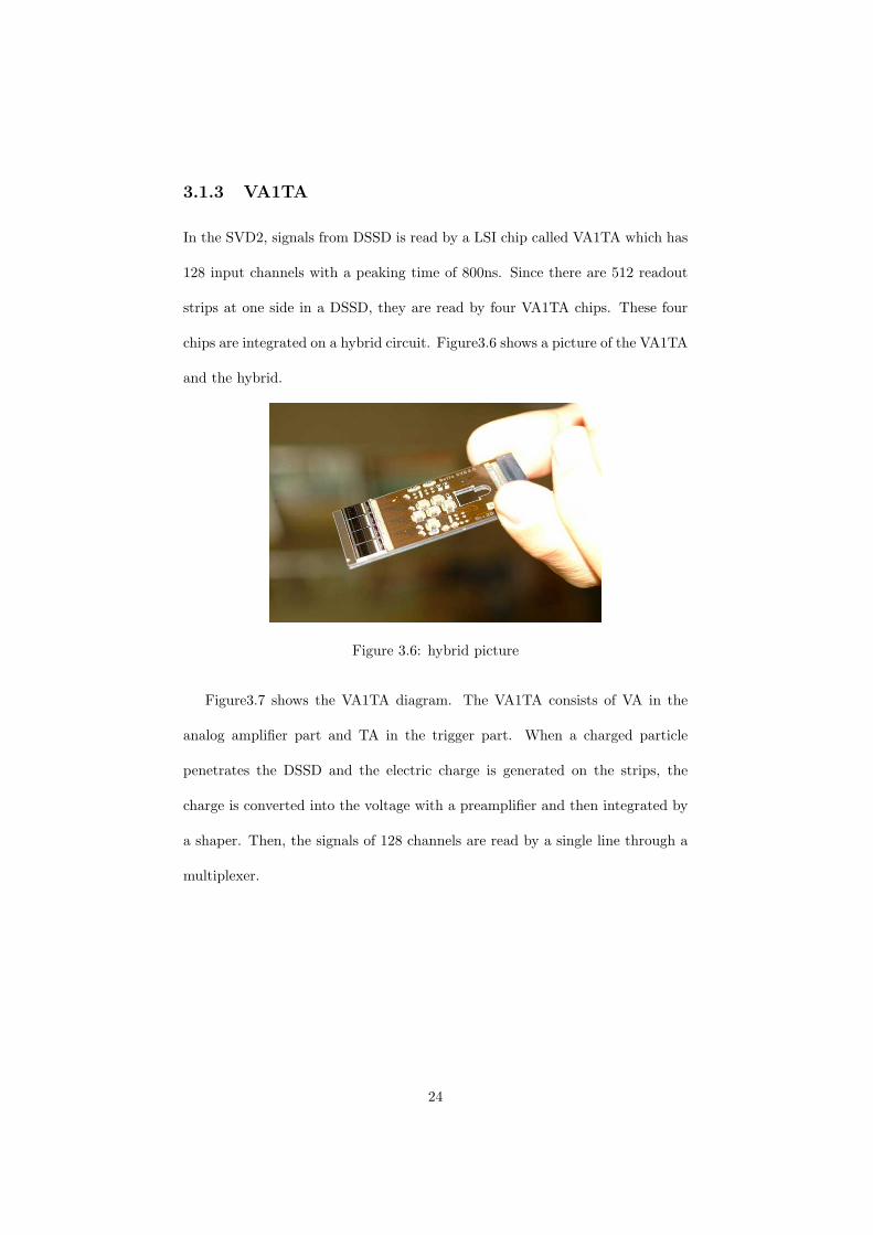
3.1.3 VA1TA
In the SVD2, signals from DSSD is read by a LSI chip called VA1TA which has
128 input channels with a peaking time of 800ns. Since there are 512 readout
strips at one side in a DSSD, they are read by four VA1TA chips. These four
chips are integrated on a hybrid circuit. Figure3.6 shows a picture of the VA1TA
and the hybrid.
Figure 3.6: hybrid picture
Figure3.7 shows the VA1TA diagram. The VA1TA consists of VA in the
analog amplifier part and TA in the trigger part. When a charged particle
penetrates the DSSD and the electric charge is generated on the strips, the
charge is converted into the voltage with a preamplifier and then integrated by
a shaper. Then, the signals of 128 channels are read by a single line through a
multiplexer.
24

Figure 3.7: VA1TA diagram
3.1.4 Readout system
Figure3.8 shows the readout system used in the SVD2. The function of each
module is explained as follows.
25
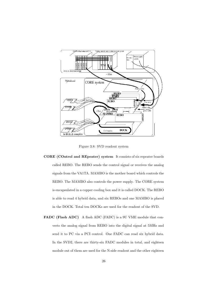
Figure 3.8: SVD readout system
CORE (COntrol and REpeater) system It consists of six repeater boards
called REBO. The REBO sends the control signal or receives the analog
signals from the VA1TA. MAMBO is the mother board which controls the
REBO. The MAMBO also controls the power supply. The CORE system
is encapsulated in a copper cooling box and it is called DOCK. The REBO
is able to read 4 hybrid data, and six REBOs and one MAMBO is placed
in the DOCK. Total ten DOCKs are used for the readout of the SVD.
FADC (Flash ADC) A flash ADC (FADC) is a 9U VME module that con-
verts the analog signal from REBO into the digital signal at 5MHz and
send it to PC via a PCI control. One FADC can read six hybrid data.
In the SVD2, there are thirty-six FADC modules in total, and eighteen
module out of them are used for the N-side readout and the other eighteen
26

are used for the P-side readout.
TTM (Trigger Timing Module) TTM is a 6U VME module that controls
the trigger signal and the DAQ system. TTM can send the signal such
as ADC start, ADC stop, busy, and 4 bit event tag to the REBO and
FADC, and it monitors and controls the readout cycle of the data. There
are eleven TTM modules in total.
Power supply Power supply provides both High Voltage (H.V) and Low Volt-
age (L.V). The H.V is the bias voltage applied to the DSSDs for the de-
pletion. The L.V is used for the front-end electronics. Each one of H.V
and L.V supply is utilized for the one DOCK, and there are ten modules
in total.
DAQ system Twelve PCs in total are used in the DAQ system of the SVD. It
reads the data sent from FADC via the PCI bus. And then, the sparsified
data are sent to the Belle event builder. One PC has three PCI boards
and can read the data for three FADC modules.
3.1.5 Performance
The typical trigger rate is ∼400Hz and the average occupancy of the SVD is
around 3 %. Under these conditions, the performance of SVD2 is good enough
as summarized in Table3.3.
S/N >16Occupancy [%] in layers 1/2/3/4 10/3.5/2.0/1.5
Hit-finding efficiency [%] 90Impact parameter resolution [µm] for dz 26.3
⊕32.9/(pβ(sinθ5/2)
Impact parameter resolution [µm] for dz 17.4⊕
34.3/(pβ(sinθ3/2)
Table 3.3: Parameters of SVD2
27

Because the technology of KEKB accelerator is developing, SVD2 will not
be able to retain its performance. Then we need to upgrade the SVD. I will
describe the upgrade in next section.
28

3.2 Upgrade of the SVD
As described in section2.2 (Figure2.5), the luminosity of the KEKB will increase.
In the present schedule, it will increase by three times in 2007. The SVD will
be exposed by more radiations, thus beam background level will increases as
shown in Figure3.9.
The occupancy, which is defined as the ratio of hit strips to all strips, in-
creases proportional to the background level. Figure3.10 shows the hit-finding
efficiency as a function of occupancy in the first layer. When occupancy in-
creases, it will be difficult to find collect hits.
Figure 3.9: Belle event-displays comparing current and 20 times higher one
To cope with this problem, we like to introduce a readout chip such as
APV25, which has a faster peaking time (∼50ns). We replaced the readout in
the first and second layer ladders, and the new SVD after this upgrade is called
SVD3. Since the peaking time of APV25 is 1/16 as fast as that of the present
readout chip VA1TA (∼800ns), the occupancy of the SVD is expected to be
29

reduced by 1/16. Details of the APV25 will be described in next section.
Figure 3.10: Hit-finding efficiency as a function of occupancy in the first layer
3.2.1 APV25
The APV25, with128 input channels, has been developed for a silicon detector
used at CMS. The feature of APV25 different from current readout VA1TA is
as below:
• Faster peaking time (∼50ns)
• Pipeline memory and sequencer
Figure 3.11: APV25 block diagram
30

As shown in Figure3.11, APV25 consists of a preamplifier, shaper, pipeline
and multiplexer. When the signal fed to the APV25 goes through a preamplifier
to a shaper, the signal is amplified and shaped with peaking time Tp=50ns.
The shaper output is sampled at clock intervals and stored in the pipeline.
The pipeline of the APV25 is a ring buffer which has 192 cells with cycling
write and read pointers. The signal stored at the pipeline is read after a certain
constant latency time. The latency time between the signal input and the trigger
is more than 4µs with 40MHz clock frequency. APV25 has the sequencer that
can generate a series of subsequent APV triggers initiated by a single hardware
trigger. By using this feature, a sequence of samples separated by a single clock
cycle can be obtained (multi-peak mode). This can be used to effectively get
subsequent samples of the shaping curve from particle signal. The output signal
from one APV chip in multi-peak mode is shown in Figure3.12.
Figure 3.12: Output signal from APV25 in a 6 sample multi-peak mode
31

3.3 Necessity of new DSSD
Because the noise from a semiconductor detector greatly depends on the detector
capacitance in the case of short peaking time, it is expected that the introduction
of APV25 causes large noise to the current DSSD.
The intrinsic noise of a semiconductor detector is mainly caused by the
detector leakage current and electric capacitance. The formula of noise from
the readout chip is,
[Intrinsic noise] = NCapa ⊕ NLeak
where NCapa and NLeak are the noises caused by the detector-capacitance and
leakage-current respectively, which are represented as follow,
CLeak ∝√
ILeakTPeak, (3.1)
CCapa ∝ CLoad√TPeak
, (3.2)
where ILeak, CLoad, TPeak is the leakage-current, the load capacitance of one
strip, and the peaking time of shaping curve.
Since the current DSSD is designed to be minimized the radiation damage,
the strip width is maximized, therefore the detector-capacitance is large. When
we introduce APV25 that has a faster peaking time, the NCapa term will be-
come dominant (Formula(3.1), (3.2)). Then, if we use the current DSSD with
APV25, the intrinsic noise will become very large, and this degrade the sensor
performance.
To solve this difficulty, we need new DSSD for capacitance reduction. Since
the capacitance of the N-side is especially larger than P-side because of the P-
stop, we prepared a prototype of N-side Single-sided Silicon-strip Detector (SSD)
32

with 5 different strip-configuration. I will show the detail of the prototype in
next chapter.
33

Chapter 4
Test sensor
The test sensor is fabricated by HPK. It is a N-side single-sided strip detec-
tor (SSD), since the capacitance of the N-side is especially larger than P-side
because of the P-stop.
4.1 Structure of the test sensor
The blue print of this sensor is shown in the Figure4.1. The test sensor has 5
regions of different structure.
34

Figure 4.1: N-side SSD blue print
The parameters of each region are shown in Table4.1. 5 regions are different
in strip pitch, strip width, and P-stop gap. Note that readout pitch in 75µm-
pitch regions is twice as wide as strip pitch, that is to say, strips in the regions
are read alternately.
S75-2 S75-3 S75-4 S100-3 S100-5Sensor size [mm] 10.7 × 32.2Active area [mm] 8.3 × 28.4 11.0 × 28.4
Strip pitch [µm] (A) 75 100Readout pitch [µm] 150 100Number of strips 12
N-strip width [µm] (B) 32 24 12 12 12P-stop width [µm] (C) 12 12 7 35 10
N-strip-P-stop gap [µm] (D) 6P-stop gap [µm] (E) 7 15 37 6 56
Table 4.1: SSD parameters
The cross section view of the SSD is shown in Figure4.2. In N-side, there
are N-strips, and P-stops to insulate neighbor strips each other in N-strip. In
P-side, the whole region is implanted by P+.
35

Figure 4.2: The cross section view of the test sensor
The detail of one region in the sensor is shown in Figure4.3. In P-side, there
are two slits perpendicular to strip direction. These slits are used for laser scan
of the sensor. And there are individual bias pads through which we are able to
apply bias voltage to individual regions.
Figure 4.3: The detail of one area in the test sensor
4.2 Test sample
Figure4.4 shows a picture of a test sample. The test sample consists of same 2
test sensors, a bias line for the bias voltage, and a hybrid with 4 APV chips.
36

Figure 4.4: Picture of a test sample
The negative bias voltage(0 to -100V) is applied from the P-side of the test
sensor. Sensor strips are connected to the APV25 chip. This test sample was
used for the beam test described in Chapter5.
4.3 DAQ system of APV25 readout
Figure4.5 shows a DAQ system of APV25 readout. The output from the APV25
chips are fed to APVDAQ through the AC Repeater.
Figure 4.5: APV DAQ system
37

Figure 4.6: APVDAQ
The APVDAQ (Figure4.6) is a 6U VME module used for the control and
readout from the APV25 chip. It consists of a Stratix Altera, a VME protocol
Altera, an ADC daughter board and supplemental electronics. On the front
panel of APVDAQ, there are an analog signal input and an output for the
controls (clock, trigger etc.), and these are connected to the Repeater with flat
cable and CAT7 cables respectively. Furthermore, there are an external clock
input and a trigger input on the front panel.
The AC reapeater is an interface between the hybrid and the APVDAQ. It
bridges signals to the floating power scheme of the APV chip for clock, trigger,
and analog signals.
The control of the DAQ system and readout of the analog data is carried
out by a PC. The data acquisition software operates with the LabWindows/CVI
38

developed by National Instruments. This software is written in the C program-
ming language.
There are several operation types in the data acquisition system. The mea-
surements are mainly performed with two operation modes: Hardware run and
Internal calibration scan run. The Hardware run is a normal operation with an
external trigger. The Internal calibration scan is used for the sampling of the
APV output waveform. From these waveform data, the peaking time and chip
gain can be calculated.
In a data acquisition, the VME board and APV are reset first. Next, APV25
chip parameters such as shaping time and number of samples are fixed. And
then 600 events of local run (Appendix A) are taken by the internal triggers.
These 600 events are used to calculate pedestal and noise. After that, a data
acquisition with Hardware run starts.
4.4 Sensor capacitance
Detector capacitance consists of two kinds of DSSD capacitance. One is the
interstrip capacitance Ci and the other is capacitance between strip and back
plane Cb.
The back plane capacitance Cb is very small compare to Ci because the
distance between P and N side, which is about 300µm, is much larger than the
strip pitch. So the interstrip capacitance Ci mainly contribute to the detector
capacitance. According to the LEP-SI model (Appendix B), Ci is a function of
the ratio of the strip width to the strip pitch.
Figure4.7 shows the bias voltage dependence of the interstrip capacitance
of each region. In this measurement, 1MHz AC voltage is applied between two
39
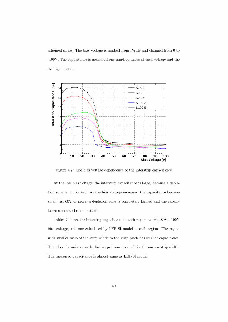
adjoined strips. The bias voltage is applied from P-side and changed from 0 to
-100V. The capacitance is measured one hundred times at each voltage and the
average is taken.
Bias Voltage [V]0 10 20 30 40 50 60 70 80 90 100
Inte
rstr
ip C
apac
itan
ce [
pF
]
0
2
4
6
8
10
12
14 S75-2
S75-3
S75-4
S100-3
S100-5
Figure 4.7: The bias voltage dependence of the interstrip capacitance
At the low bias voltage, the interstrip capacitance is large, because a deple-
tion zone is not formed. As the bias voltage increases, the capacitance become
small. At 60V or more, a depletion zone is completely formed and the capaci-
tance comes to be minimized.
Table4.2 shows the interstrip capacitance in each region at -60, -80V, -100V
bias voltage, and one calculated by LEP-SI model in each region. The region
with smaller ratio of the strip width to the strip pitch has smaller capacitance.
Therefore the noise cause by load-capacitance is small for the narrow strip width.
The measured capacitance is almost same as LEP-SI model.
40

S75-2 S75-3 S75-4 S100-3 S100-5-60V 2.3pF 2.0pF 1.7pF 1.2pF 1.5pF-80V 2.1pF 1.9pF 1.6pF 1.2pF 1.4pF-100V 2.0pF 1.8pF 1.6pF 1.2pF 1.3pF
LEP-SI model 2.3pF 2.0pF 1.5pF 1.4pF 1.4pF
Table 4.2: SSD interstrip capacitance
41

Chapter 5
Beam test analysis
In this chapter, I will describe the detail of the beam test ducted at KEK in
December, 2005. The purpose of this test is to measure spatial resolution and
hit-finding efficiency of the test sensor with APV25 readout, which is described
in chapter4.
5.1 Condition of the beam test
5.1.1 Outline
The beam test was performed at the KEK/PS π2 beam line (Figure5.1) in
December, 2005. Since the perpendicular 4GeV/c π− beam are obtained, we
can precisely measure the performance of the test sensor as same as that in real
operation.
42

Figure 5.1: The beam line in KEK/PS
5.1.2 Test detector system
A layout and a picture of the test detector are shown in Figure5.2 and Figure5.3.
The test detector of the beam test includes the test sample described in
chapter4 and three DSSD ladders. These DSSD ladders are for the telescope,
and are the spare of layer-1 ladders of SVD2 but slightly different from the
currently operated SVD2 ones: there is no aluminum electnode pad on the
floating strip in P-side.
Figure 5.2: Test detector layout
43

Figure 5.3: Test detector picture
5.1.3 Readout system
Figure5.4 shows a schematic diagram of the readout system at the beam test.
We operated the APV25 and VA1TA synchronously as same as we will in SVD3
operation. A test sample is read by the readout of APV25, and three DSSDs
are read by the readout of VA1TA. For the readout of the APV25, APVDAQ
explained in Section4.3 is used, and for the readout of the VA1TA, the same
system as the actual SVD readout described in Section3.1.4 are used.
A trigger signal is generated by taking the coincidence of the signal of two
scintillation counters. This signal is fed to the APVDAQ and TTM. After
trigger acceptance, a veto signal is issued from both APVDAQ and TTM. By
using the veto signal, we can avoid the event slip between APV25 and VA1TA.
The VA1TA data has a 4bit event tag. It is also sent to the APVDAQ , and we
can match the event between APV25 and VA1TA data acquisition.
44

Figure 5.4: A Schematic diagram of readout system at the beam test
45

5.2 Analysis procedure
The data used for the analysis were taken with 50ns peaking time, 12 sample
multi-peak mode, and -80V bias voltage. The analysis procedure is as follow.
1. A data sparsicication and clustering to find the hit position
2. Reconstruction of the proper track by using the hit position
3. Calculation of the deviation of residual on the prototype-sensor
After all, we can obtain the spatial resolution and hit-finding efficiency.
5.2.1 Data sparcification
First, I mention the raw data. As concerns the raw data read by VA1TA readout,
the trigger timing was adjusted so that the data becomes shaping. On the other
hand, one read by AVP25 readout, 12 sample data are taken with an interval of
25ns in one event. At this run, we fixed to use the 4th sample data as the raw
data.
As shown in Equation(5.1), the raw data (Raw) consists of signal charge
yield (S), pedestal (P), and common-mode-shift (CMS). S is composed of signal
deriving from particles (Sparticle) and from intrinsic-noise (Snoise), and these
can’t be distinguished. S is obtained after subtracting pedestal and CMS. P and
RMS of Sparticle (N) can be calculated in 600 events of local run (Appendix A).
Raw = S + P + CMS (5.1)
During the performance, we calculated CMS at each event. When signal-to-
noise ratio on a strip is larger than 3 (S/N>3), we define it as a ”hit strip”. In
calculation of CMS we removed all hit strips, then we can consider that S of
remaining strips doesn’t include Sparticle as same as the local run.
46

We define Snoise as vanishing by summing up over all hit strips (as same as
Appendix A Equation A.1). CMS at a certain event is obtained by averaging
pedestal-subtracted ADC counts,
CMS =∑
h (Rawh − Ph)[Number of hit strips]
(5.2)
where Rawh, Ph is raw data and signal charge yield at h-th hit strip.
5.2.2 Clustering
To find a hit signal and its hit position, first we define a cluster. When a charged
particle goes through the sensor, the hit signal consists of two or more adjoined
strips. This is called a cluster. We reconstruct clusters based on the observed
signal charge yield(S).
1. Search for a ”cluster seed” strip, whose S/N is larger than the cluster-
seed-threshold(Cseed) and S is largest in all strips.
2. Define ”cluster tail” strips, if the S/N of the neighboring strips of the
cluster seed strip is larger than the cluster-tail-threshould (Ctail).
3. Without selected strips, repeat 1∼2 procedure while cluster seed can be
found.
Moreover we select clusters whose cluster signal to noise ratio(Scluster/Ncluster)
is larger than Ccluster as follows,
Scluster/Ncluster =∑
i Si√∑i Ni
2, (5.3)
In this analysis, Cseed, Cstrip, and Cclust is set to 5.0, 3.0, and 10.0, respectively.
The cluster reconstruction of VA1TA data is also performed with the same
manner. We combine the APV25 and VA1TA data based on the event tag
47
information. Then, we select an event that has cluster signals in the all four
layers.
The beam hit position is calculated using the center of gravity method using
the cluster. Because the SSD is used, only the one dimension position informa-
tion can be obtained.
5.2.3 Reconstruction of track
To obtain a proper track, we used three DSSDs with VA1TA system for tele-
scope. The alignment of these DSSDs are well-corrected (Appendix C).
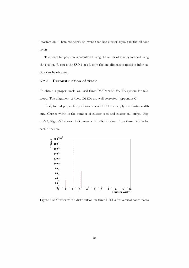
First, to find proper hit positions on each DSSD, we apply the cluster width
cut. Cluster width is the number of cluster seed and cluster tail strips. Fig-
ure5.5, Figure5.6 shows the Cluster width distribution of the three DSSDs for
each direction.
Cluster width0 1 2 3 4 5 6 7 8 9 10
En
trie
s
0
20
40
60
80
100
120
140
160
180
200310×
Figure 5.5: Cluster width distribution on three DSSDs for vertical coordinates
48

Cluster width0 1 2 3 4 5 6 7 8 9 10
En
trie
s
0
20
40
60
80
100
120
140
160
180
200310×
Figure 5.6: Cluster width distribution on three DSSDs for horizontal coordinates
The π− beam is injected so perpendicularly that cluster width of most of clusters
is 1∼3. I selected clusters whose width is less than 4 (red-slashed portion).
However, since there are one or more such selected positions on each DSSDs
for each direction, what we have obtained is the candidate of proper hit posi-
tions. To reconstruct a proper set of such positions, first we fit linear tracks
for all possible sets of hit position. Next we select the track and the set of
position whose χ2 is minimum, where we assume that three DSSDs have the
same intrinsic-spatial-resolution. For example as Figure5.7, there are 2-1-2 hit
positions(point X) in the three DSSD system. We can fit 4 possible tracks(black-
dotted and red arrows). Red one has minimum χ2, then we select the track and
concerning positions.
49
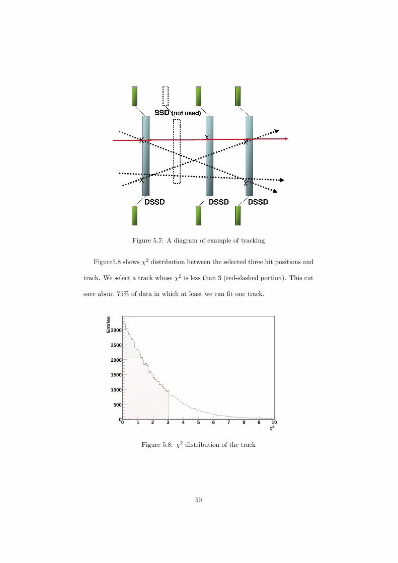
Figure 5.7: A diagram of example of tracking
Figure5.8 shows χ2 distribution between the selected three hit positions and
track. We select a track whose χ2 is less than 3 (red-slashed portion). This cut
save about 75% of data in which at least we can fit one track.
2χ0 1 2 3 4 5 6 7 8 9 10
En
trie
s
0
500
1000
1500
2000
2500
3000
Figure 5.8: χ2 distribution of the track
50

5.2.4 Calculation of the sigma of residual
In this section, I will calculate the sigma of residual (σresidual) on test sensor
with APV25 readout. Residual is represented by this formula.
[Residual] = [Hit position] − [Track-estimated position]
Similar to three DSSDs, there may be one or more hits in a region of the test
sensor. For calculation of the residual, we select one which is nearest to the
estimated position by the proper track (described in Section5.2.3).
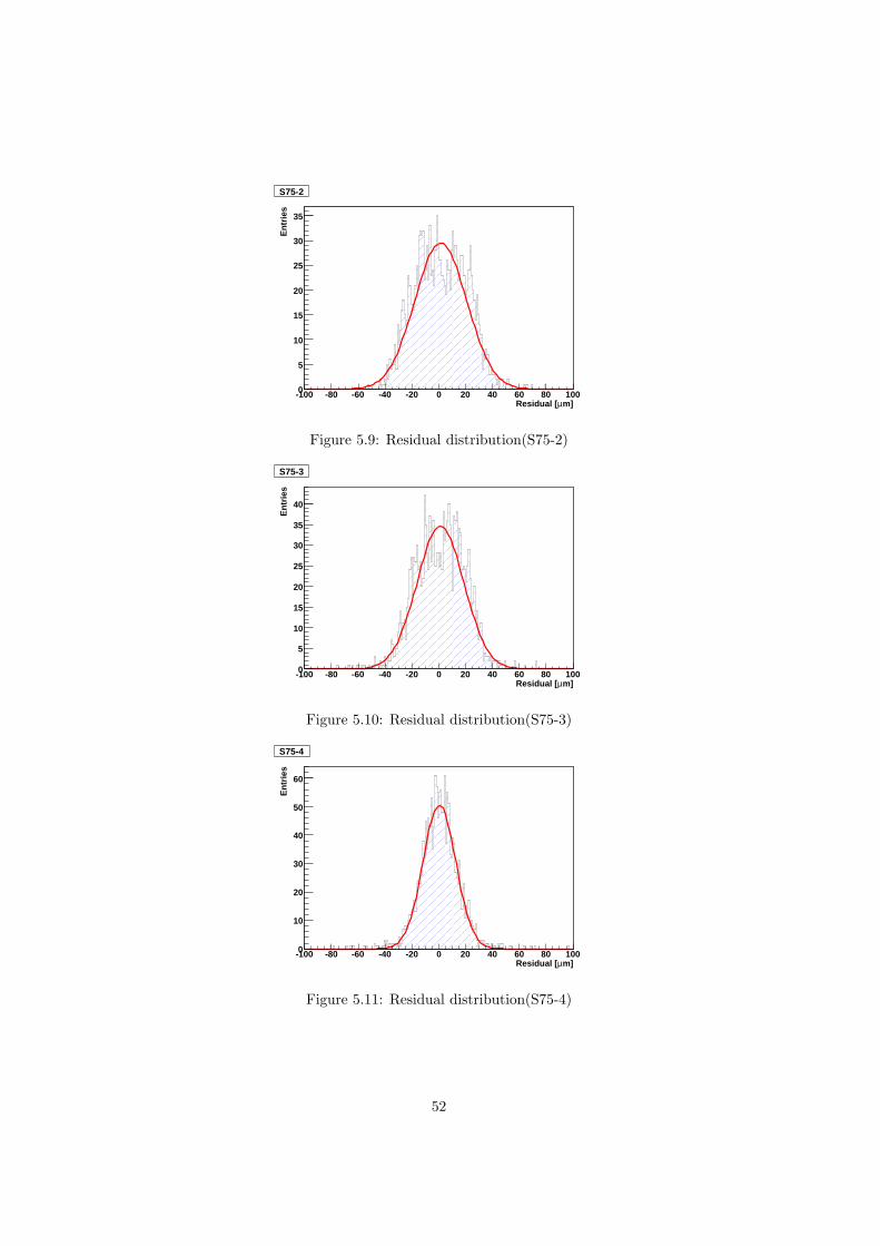
Then, we can plot the residual distribution in each region of test sensor as
shown in Figure5.9∼5.13. σresidual is obtained by the gaussian fit as shown in
Table5.2.4.
We define the Proper-hit on the test sensor which is in 3σresidual search
window (Equation5.4).
Proper hit : | [Residual] | < 3σresidual (5.4)
Type S75-2 S75-3 S75-4 S100-3 S100-5σresidual [µm] 19.4 17.5 12.3 24.5 11.9
Table 5.1: Table of σresidual
51
m]µResidual [-100 -80 -60 -40 -20 0 20 40 60 80 100
En
trie
s
0
5
10
15
20
25
30
35
S75-2
Figure 5.9: Residual distribution(S75-2)
m]µResidual [-100 -80 -60 -40 -20 0 20 40 60 80 100
En
trie
s
0
5
10
15
20
25
30
35
40
S75-3
Figure 5.10: Residual distribution(S75-3)
m]µResidual [-100 -80 -60 -40 -20 0 20 40 60 80 100
En
trie
s
0
10
20
30
40
50
60
S75-4
Figure 5.11: Residual distribution(S75-4)
52

m]µResidual [-100 -80 -60 -40 -20 0 20 40 60 80 100
En
trie
s
0
5
10
15
20
25
30
35
40
S100-3
Figure 5.12: Residual distribution(S100-3)
m]µResidual [-100 -80 -60 -40 -20 0 20 40 60 80 100
En
trie
s
0
20
40
60
80
100
120
S100-5
Figure 5.13: Residual distribution(S100-5)
53

5.3 Experiment result
5.3.1 Hit-finding efficiency
We define the denominator and numerator of hit-finding efficiency as follows.
• The denominator: Number of hits which pass thorough acceptance region
• The numerator: Number of hits in the 3σresidual search window
(Number of Proper-hits described in Section5.2.4)
Figure5.14 shows the definition of the acceptance region and search window. The
acceptance region is the region where the strips connected to readout actually
exists. The 3σresidual search window is represented as follows.
|[Hit position] − [Estimated position by track]| < 3σresidual (5.5)
Figure 5.14: A diagram of the region definition for hit-finding efficiency
Table5.2 shows the hit-finding efficiency for each region. For all regions,
hit-finding efficiency is good enough (∼99%).
54
Type Entries Hit-finding efficiency(%)S75-2 1240/1245 99.6±0.2%S75-3 1333/1349 98.8±0.3%S75-4 1349/1371 98.4±0.3%S100-3 1891/1902 99.4±0.2%S100-5 2662/2699 98.6±0.2%
Table 5.2: Hit-finding efficiency of the test sensor
5.3.2 Signal to noise ratio
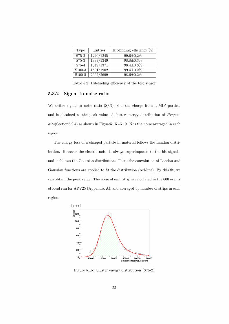
We define signal to noise ratio (S/N). S is the charge from a MIP particle
and is obtained as the peak value of cluster energy distribution of Proper-
hits(Section5.2.4) as shown in Figure5.15∼5.19. N is the noise averaged in each
region.
The energy loss of a charged particle in material follows the Landau distri-
bution. However the electric noise is always superimposed to the hit signals,
and it follows the Gaussian distribution. Then, the convolution of Landau and
Gaussian functions are applied to fit the distribution (red-line). By this fit, we
can obtain the peak value. The noise of each strip is calculated in the 600 events
of local run for APV25 (Appendix A), and averaged by number of strips in each
region.
Cluster energy [Electrons]0 10000 20000 30000 40000 50000 60000
En
trie
s
0
20
40
60
80
100
120
S75-2
Figure 5.15: Cluster energy distribution (S75-2)
55

Cluster energy [Electrons]0 10000 20000 30000 40000 50000 60000
En
trie
s
0
20
40
60
80
100
120
140
S75-3
Figure 5.16: Cluster energy distribution (S75-3)
Cluster energy [Electrons]0 10000 20000 30000 40000 50000 60000
En
trie
s
0
20
40
60
80
100
120
140
S75-4
Figure 5.17: Cluster energy distribution (S75-4)
Cluster energy [Electrons]0 10000 20000 30000 40000 50000 60000
En
trie
s
0
50
100
150
200
250
S100-3
Figure 5.18: Cluster energy distribution (S100-3)
56

Cluster energy [Electrons]0 10000 20000 30000 40000 50000 60000
En
trie
s
0
50
100
150
200
250
300
S100-5
Figure 5.19: Cluster energy distribution (S100-5)
Table5.3 shows the peak value of the cluster energy distribution, noise, and
S/N value, where ENC is Equivalent Noise Charge. S/N is required to be more
than 20 for the belle experiment, and that is satisfied at all configurations.
Type S75-2 S75-3 S75-4 S100-3 S100-5Cluster energy [Electrons] 24402 23788 20739 24846 22345
Noise [ENC] 719 674 657 826 856S/N 33.9 35.3 31.6 30.1 26.1
Table 5.3: Table of Spatial resolution of the test sensor
5.3.3 Spatial resolution
We can estimate the spatial resolution by Equation(5.6),
[Spatial resolution] =√
σ2residual + σ2
tracking + σ2multi (5.6)
where σtracking is the uncertainty of estimated position, and σmulti is the mul-
tiple scattering contribution to the spatial resolution. σtracking is calculated in
Appendix C, and it is 6.3 µm. σmulti is estimated at 1.3 µm by a GEANT4 sim-
ulation. σresidual is estimated in Section5.2.4, then we can calculate the spatial
resolution of test sensor with APV25 readout as shown in Table5.4.
57

Type S75-2 S75-3 S75-4 S100-3 S100-5Spatial resolution [µm] 18.2±0.4 16.2±0.4 10.4±0.3 23.6±0.4 10.0±0.2
Table 5.4: Table of Spatial resolution of the test sensor
5.3.4 Charge sharing
To understand how the charge from particles in the sensor is shared by one or
more sensors, I will show the correlation of the sensors and how many strips
counts the signal in a event.
The mean of cluster width is shown in Table5.5. The large mean value of
cluster width suggest that the charge deposited in the sensor is well-shared by
two or more strips.
S75-2 S75-3 S75-4 S100-3 S100-5P-stop gap [µm] 7 15 37 6 56
Mean of cluster width 1.49 1.52 1.68 1.23 1.63
Table 5.5: The mean of cluster width
In Figure5.20∼5.29, the left hand shows the cluster width distribution of hits.
The right hand shows the correlations of measured position and the estimated
position by the telescope in each region of the test sensor: the vertical axis is
the measured position, and the horizontal axis is the estimated position by the
telescope. Red, Green, Blue plots are corresponding to hits with cluster width
1, 2, 3 respectively. Positions in both axis are divided by readout pitch and the
remainder are plotted, that is, in plots of 75µm pitch sensors, the readout strips
are located at 0 and 150µm (floating strips are at 75µm), and in plots of 100µm
pitch sensors, the readout strips are located at 0 and 100µm.
The slope becomes gradual around strip-existing position in all plots. How-
58

ever, there is a notable thing. The sensor with wide P-stop gap behaves as if it
has a floating strip. For example, S100-5 has no floating strips, but the slope is
gradual around the middle of readout strips.
59
Cluster Width0 0.5 1 1.5 2 2.5 3 3.5 4
En
trie
s
0
200
400
600
800
1000
1200
1400
1600
1800
2000
2200
S75-2 hreg[2][0]Entries 1901Mean 1.492RMS 0.5337
S75-2
Figure 5.20: Cluster width distributionof hits (S75-2)
m]µEstimated position (mod:strip pitch) [0 20 40 60 80 100 120 140 160
m]
µM
easu
red
po
siti
on
(m
od
:str
ip p
itch
) [
0
20
40
60
80
100
120
140
160
S100-5S100-5
Figure 5.21: The correlation of the mea-sured and estimated position (S75-2)
Cluster Width0 0.5 1 1.5 2 2.5 3 3.5 4
En
trie
s
0
200
400
600
800
1000
1200
1400
1600
1800
2000
2200
S75-3 hreg[2][1]Entries 1998Mean 1.517RMS 0.5413
S75-3
Figure 5.22: Cluster width distributionof hits (S75-3)
m]µEstimated position (mod:strip pitch) [0 20 40 60 80 100 120 140 160
m]
µM
easu
red
po
siti
on
(m
od
:str
ip p
itch
) [
0
20
40
60
80
100
120
140
160
S100-5S100-5
Figure 5.23: The correlation of the mea-sured and estimated position (S75-3)
Cluster Width0 0.5 1 1.5 2 2.5 3 3.5 4
En
trie
s
0
200
400
600
800
1000
1200
1400
1600
1800
2000
2200
S75-4 hreg[2][2]Entries 1878Mean 1.679RMS 0.5548
S75-4
Figure 5.24: Cluster width distributionof hits (S75-4)
m]µEstimated position (mod:strip pitch) [0 20 40 60 80 100 120 140 160
m]
µM
easu
red
po
siti
on
(m
od
:str
ip p
itch
) [
0
20
40
60
80
100
120
140
160
S100-5S100-5
Figure 5.25: The correlation of the mea-sured and estimated position (S75-4)
60

Cluster Width0 0.5 1 1.5 2 2.5 3 3.5 4
En
trie
s
0
200
400
600
800
1000
1200
1400
1600
1800
2000
2200
S100-3 hreg[2][3]Entries 2590Mean 1.227RMS 0.4269
S100-3
Figure 5.26: Cluster width distributionof hits (S100-3)
m]µEstimated position (mod:strip pitch) [0 20 40 60 80 100
m]
µM
easu
red
po
siti
on
(m
od
:str
ip p
itch
) [
0
20
40
60
80
100
S100-5S100-5
Figure 5.27: The correlation of the mea-sured and estimated position (S100-3)
Cluster Width0 0.5 1 1.5 2 2.5 3 3.5 4
En
trie
s
0
200
400
600
800
1000
1200
1400
1600
1800
2000
2200
S100-5 hreg[2][4]Entries 3434Mean 1.627RMS 0.529
S100-5
Figure 5.28: Cluster width distributionof hits (S100-5)
m]µEstimated position (mod:strip pitch) [0 20 40 60 80 100
m]
µM
easu
red
po
siti
on
(m
od
:str
ip p
itch
) [
0
20
40
60
80
100
S100-5S100-5
Figure 5.29: The correlation of the mea-sured and estimated position (S100-5)
61

5.3.5 Results and discussions
Table5.6 shows all the analysis results.
S75-2 S75-3 S75-4 S100-3 S100-5Strip pitch [µm] 75 75 75 100 100
(Readout pitch) [µm] (150) (150) (150) (100) (100)N-strip width [µm] 32 24 12 12 12P-stop width [µm] 12 12 7 35 10P-stop gap [µm] 7 15 37 6 56
Interstrip capacitance [pF] 2.1 1.9 1.6 1.2 1.4(at -80V bias voltage)Hit-finding efficiency [%] 99.6±0.2 98.8±0.3 98.4±0.3 99.4±0.2 98.6±0.2Cluster energy [Electrons] 24402 23788 20739 24846 22345
Noise [ENC] 719 674 657 826 856S/N 33.9 35.3 31.6 30.1 26.1
Mean value of cluster width 1.49 1.52 1.68 1.23 1.63Spatial resolution [µm] 18.2±0.4 16.2±0.4 10.4±0.3 23.6±0.4 10.0±0.2
Spatial resolution per strip pitch 0.24 0.22 0.14 0.24 0.10
Table 5.6: All the analysis results
We did a beam test to evaluate the performance of a prototype N-side SSD
with APV25 readout. For all configurations, we confirmed the good hit-finding
efficiency (∼99%), and enough S/N of the sensor (required to be more than 20).
S100-3 and S100-5, which are different only in the P-stop structure, have
almost same detector capacitance, but the spatial resolution is quite different.
I plot the spatial resolution as a function of the mean value of cluster width
as shown in Figure5.30. The better resolution is due to the larger mean value.
We can consider that when the charge from particle is well-shared by multiple
strips, the spatial resolution becomes good. Moreover in the region with good
resolution like S100-5, the sensor behaves as if it has a floating strip in the
middle of two strips where actually there are no strip (Section5.3.4). This effect
seems to enhance the ability of charge sharing.
To confirm what cause the well charge sharing, I plot the mean value of
62

cluster width as a function of P-stop gap (Figure5.31). The larger mean value of
cluster width is due to the wider P-stop gap. Thus, the better spatial resolution
is due to the wider P-stop gap as shown in Figure5.32.
Mean value of cluster width1.1 1.2 1.3 1.4 1.5 1.6 1.7 1.8
m)
µ)
(A
PV
σS
pat
ial r
eso
luti
on
(
0
5
10
15
20
25
30
m]µStrip pitch 75 [
m]µStrip pitch 100 [
Figure 5.30: The spatial resolution vs Mean value of cluster width
m]µP-stop gap [0 10 20 30 40 50 60
Mea
n v
alu
e o
f cl
ust
er w
idth
1
1.1
1.2
1.3
1.4
1.5
1.6
1.7
1.8
1.9
2
m]µStrip pitch 75 [
m]µStrip pitch 100 [
Figure 5.31: The P-stop gap dependence of mean value of cluster width
63

m]µP-stop gap [0 10 20 30 40 50 60
m]
µS
pat
ial r
eso
luti
on
[
0
5
10
15
20
25
m]µStrip pitch 75 [
m]µStrip pitch 100 [
Figure 5.32: P-stop gap dependence of the spatial resolution
64

Chapter 6
Summary and Conclusion
The employment of APV25 readout chip for SVD readout causes increase of the
noise from detector capacitance. Then we have to design new DSSD, and we
prepare the prototype of the sensor with 5 configurations.
The purpose of this thesis is to evaluate and study the performance of new-
designed sensor with APV25 readout. First we measured the capacitance be-
tween neighboring strips since it is dominant component of detector capacitance.
At the -80V bias voltage which is high enough for the semiconductor to be full-
depleted, the measured capacitance is almost same as that of LEP-SI model
(Appendix B) which suggests that the sensor with smaller ratio of the strip
width to the strip pitch has smaller capacitance.
To measure the performance of the prototype on the close condition to the
real operation, we did a beam test by using 4GeV π− beam. For all configu-
rations, we confirm the good hit-finding efficiency (∼99%), and enough S/N of
the sensor (required to be more than 20). About the spatial resolution of the
sensor, I find the sensor with wider P-stop gap has better resolution. When
P-stop gap is wide, the mean value of cluster width becomes large because the
charge from particles passing between two strips are well-shared to both strips,
65

and this results in the good spatial resolution.
However we have not understood why wider P-stop gap causes the well
charge sharing, and the solution of this question is one of the future studies for
the silicon strip sensor. As another future task, we have to study the influence
of the radiation damage. The radiation dose of the SVD is expected to increase,
and especially the leakage current of the sensor increases by γ-ray irradiation,
which causes the larger shot noise. Thus, we need to evaluate its radiation
hardness by irradiating γ-rays to the sensor.
66

Appendix A
Local run
DAQ system of APV25 readout takes first 600 events for pedestal and noise
evaluation by the internal random trigger.
We define,
600∑eve=1
Snoise(eve, ch) = 0,128∑
ch=1
Snoise(eve, ch) = 0 (A.1)
where Snoise(eve,ch) is the signal witch derives from intrinsic noise depending
on the event and channel. And define,
600∑eve=1
CMS(eve, ch) = 0 (A.2)
where CMS(eve) is common-mode-shift which depend on the event. CMS is the
external noise which influences the entire chip, and whose ADC counts change
with the same amount for all channels.
In this run, we can consider that there are no signals deriving from particles.
Then, the ADC counts of the local run is shown as follows,
ADC(eve, ch) = Snoise(eve, ch) + P (ch) + CMS(eve) (A.3)
where P(ch) is pedestal. The pedestal is an offset ADC value of each channel.
67
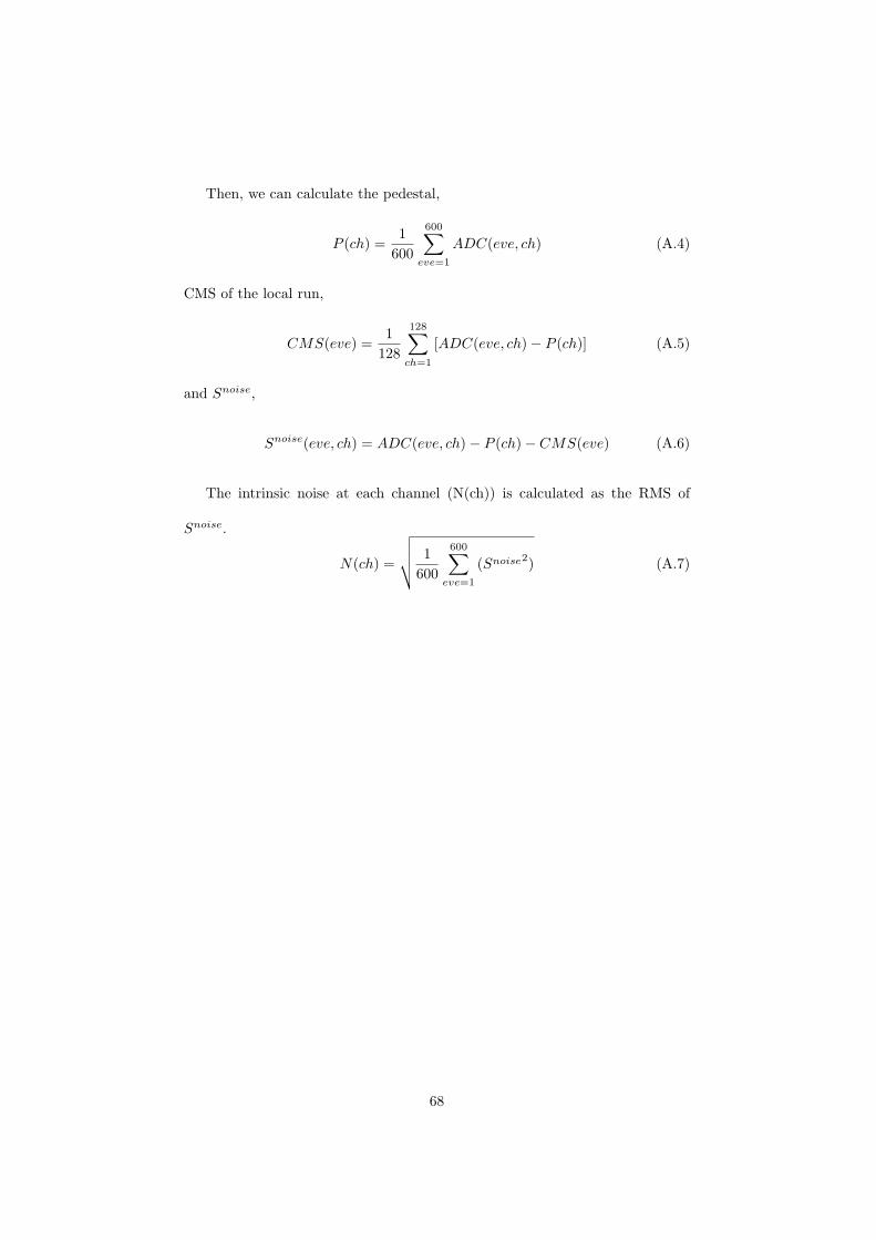
Then, we can calculate the pedestal,
P (ch) =1
600
600∑eve=1
ADC(eve, ch) (A.4)
CMS of the local run,
CMS(eve) =1
128
128∑ch=1
[ADC(eve, ch) − P (ch)] (A.5)
and Snoise,
Snoise(eve, ch) = ADC(eve, ch) − P (ch) − CMS(eve) (A.6)
The intrinsic noise at each channel (N(ch)) is calculated as the RMS of
Snoise.
N(ch) =
√√√√ 1600
600∑eve=1
(Snoise2) (A.7)
68

Appendix B
LEP-SI model
LEP-SI model is used for the estimation of the detector capacitance. the details
of this model is describe in [3] and [7].
A DSSD has a finite number of strips with a certain width placed regularly.
In this model, the interstrip capacitance Ci is a function of the ratio of strip
width W to strip pitch p.
Ci =
επ ln(2 1+
√k
1−√
k)L 0≤k≤0.7
επ
ln(2 1+√
k′
1−√
k′)L 0.7≤k≤1.0 (B.1)
where k = W/p, k′ =√
1 − k2, ε is the dielectric constant of silicon, and L is
the strip length. FigureB.1 shows the calculated capacitance as a function of k
with L = 30mm.
strip width/strip pitch0 0.1 0.2 0.3 0.4 0.5 0.6 0.7 0.8 0.9 1
strip width/strip pitch0 0.1 0.2 0.3 0.4 0.5 0.6 0.7 0.8 0.9 1
inte
rstr
ip C
[pF
]
0
1
2
3
4
5
6
7
8
9
10
Figure B.1: The plot of interstrip capacitance at LEP-SI model
69

Appendix C
Alignment and the spatialresolution of current DSSDs
We put three DSSDs carefully, but they may not precisely line up. Then we
have to correct the coordinates of them. Here we define the upstream one as
DSSD1, the middle one as DSSD2, and the downstream one as DSSD3.
There are two assumption.
1. All three DSSDs have the same spatial resolution.
2. DSSD1 and DSSD3 are perfectly aligned.
(Even if DSSD1 and 3 are actually not well-aligned, we can’t distinguish
whether they are not well-aligned or the beam incidence is not perpendic-
ular.)
Then we correct the coordinates of DSSD2. FigureC.1 is the diagram of
alignment. First, we connect the hit of DSSD1 and that of DSSD3 with a line.
If DSSD2 is perfectly aligned, the hit of DSSD2 comes just on the line. We plot
the difference between the hit of DSSD2 and the line, and obtain the sigma of
the distribution (σdiff ). We rotate DSSD2 on the plane vertical to the beam
70
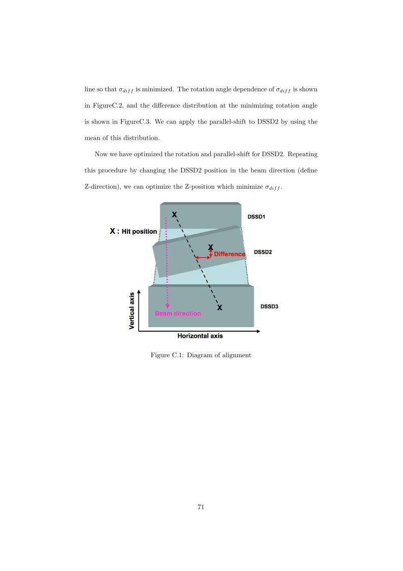
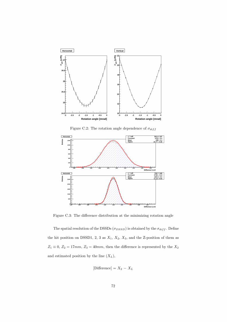
line so that σdiff is minimized. The rotation angle dependence of σdiff is shown
in FigureC.2, and the difference distribution at the minimizing rotation angle
is shown in FigureC.3. We can apply the parallel-shift to DSSD2 by using the
mean of this distribution.
Now we have optimized the rotation and parallel-shift for DSSD2. Repeating
this procedure by changing the DSSD2 position in the beam direction (define
Z-direction), we can optimize the Z-position which minimize σdiff .
Figure C.1: Diagram of alignment
71
Rotation angle [mrad]
-3 -2.5 -2 -1.5 -1 -0.5 0
m]
µ [
dif
fσ
24.5
25
25.5
26
26.5
27
HorizontalHorizontal
Rotation angle [mrad]
-3 -2.5 -2 -1.5 -1 -0.5 0m
]µ
[d
iff
σ10
12
14
16
18
20
22
VerticalVertical
Figure C.2: The rotation angle dependence of σdiff
m]µDifferece [-280 -260 -240 -220 -200 -180 -160 -140 -120 -100
En
trie
s
0
200
400
600
800
1000
1200
Horizontal / ndf 2χ 501.4 / 197Constant 5.3± 1212 Mean 0.1± -188 Sigma 0.06± 24.77
Horizontal
m]µDifferece [-320 -300 -280 -260 -240 -220 -200 -180 -160 -140
En
trie
s
0
500
1000
1500
2000
2500
Horizontal / ndf 2χ 739.7 / 168Constant 11.9± 2728 Mean 0.0± -220.4 Sigma 0.03± 11.12
Horizontal
Figure C.3: The difference distribution at the minimizing rotation angle
The spatial resolution of the DSSDs (σDSSD) is obtained by the σdiff . Define
the hit position on DSSD1, 2, 3 as X1, X2, X3, and the Z-position of them as
Z1 ≡ 0, Z2 = 17mm, Z3 = 40mm, then the difference is represented by the X2
and estimated position by the line (XL),
[Difference] = X2 − XL
72

then,
σdiff =√
σ2DSSD + σ2
Line (C.1)
where σLine is the uncertainty of XL which is,
XL =(Z3 − Z2)X1 + Z2X3
Z3(C.2)
then,
σLine =
√(Z3 − Z2)2 + Z2
2
Z3σDSSD (C.3)
where Z3 are pre-known constant and Z2 is earlier optimized one. Then we can
calculate σDSSD by EquationC.1, C.3 and the difference distribution as shown
in TableC, where P-side read the horizontal coordinate, and N-side is to the
vertical coordinate.
Type P-side N-sideσDSSD [µm] 20.2±0.09 9.1±0.04
Table C.1: Table of σDSSD
As same as this calculation, we can calculate the uncertainty of track (σTrack)
described in Section5.2.3. The track parameter A, B (X = AZ +B) is found as
follows.
A =3(
∑3i=1 ZiXi) − (
∑3i=1 Zi)(
∑3i=1 Xi)
3(∑3
i=1 Z2i ) − (
∑3i=1 Zi)2
(C.4)
B =(∑3
i=1 Zi)2(∑3
i=1 Xi) − (∑3
i=1 ZiXi)(∑3
i=1 Zi)
3(∑3
i=1 Z2i ) − (
∑3i=1 Zi)2
(C.5)
Define the estimated position by the track, and Z-position of the test sensor as
XTrack, and Za,
XTrack = AZa + B (C.6)
73

Then by using EquationC.4∼C.6 and σDSSD,
σtrack =
√√√√∑3j=1 [(3Zj −
∑3i=1 Zi)Za + (
∑3i=1 Zi
2) − (∑3
i=1 Zi)Zj ]2
[3(∑3
i=1 Z2i ) − (
∑3i=1 Zi)2]
2 × σDSSD
(C.7)
The test sensor only read the vertical coordinate, and finally we obtain σtrack
by using σDSSD(N-side).
σtrack = 6.34 [µm] (C.8)
74
Bibliography
[1] M.Friedl (Vienna University of Technology) Doctor Thesis (2001)
[2] M. Friedl, APVDAQ Reference Manual.
[3] R.Abe (Niigata University) Master Thesis (2002)
[4] S.Ono (T.I.T) Master Thesis (2006)
[5] Y.Nakahama (Tokyo University) Master Thesis (2006)
[6] J.Kaneko (T.I.T) IEEE Trans. Nucl.Sci., VOL49,NO.4 (2002),1593
[7] D.Hussun IEEE Trans. Nucl.Sci., VOL41,NO.4 (1994),811
[8] The Belle Collaboration The Belle detector [KEK Progress Report 2000-4]
[9] Y.Fujisawa (Tohoku University) Master Thesis (2002)
[10] H.Yamamoto (Tohoku University) Lecture notes [Quantum Field Theory]
[11] Y.Fujisawa (Tohoku University) Master Thesis (2002)
[12] N.Kikuchi (Tohoku University) Master Thesis (2006)
75


