Maria Concetta Allia - Silvaco · Maria Concetta Allia Device ... The User defined option allows to...
63
Device simulation Maria Concetta Allia
Transcript of Maria Concetta Allia - Silvaco · Maria Concetta Allia Device ... The User defined option allows to...

Device simulation
Maria Concetta Allia

2
Maria Concetta Allia DeviceIMS CAD & Design Services
Atlas overview
Atlas is a physically-based two and three dimensional device simulator that predicts the electrical behavior of semiconductor devices at specified bias conditions.
The physical structures simulated with Athena are used as input by Atlas.
The combination of Athena and Atlas makes possible to determine the impact of process parameters on device characteristics.
Atlas simulation
Generating Atlas input file
Running Atlas simulation
Analyzing Atlas output file
Atlas input file
It is a text file that can be arranged by using Deckbuild or any text editor.
It collects a sequence of commands (statements) corresponding to required bias conditions and control commands specified to select physical models and parameters.

3
Maria Concetta Allia DeviceIMS CAD & Design Services
Simulation problem specification
The simulation problem must be specified in the input file, defining the following steps:
The physical structure to be simulated.
The physical models to be used.
The numerical methods needed to solve the physical equations.
The bias conditions for the electrical characteristics.
The present section describes how to perform these steps.
4
Maria Concetta Allia DeviceIMS CAD & Design Services
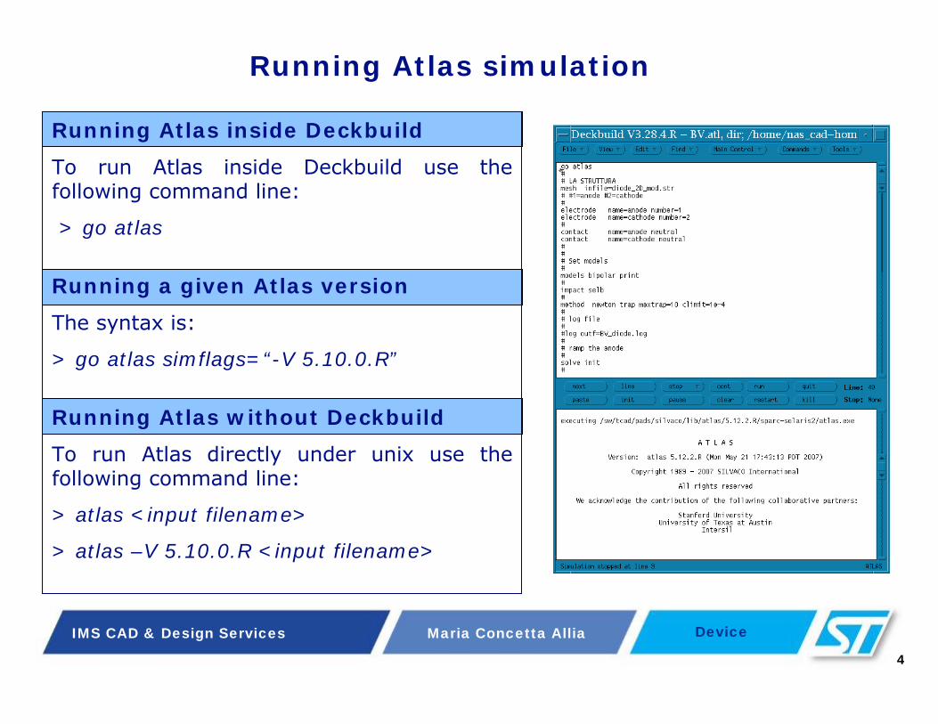
Running Atlas simulation
Running Atlas inside Deckbuild
To run Atlas inside Deckbuild use the following command line:
> go atlas
Running a given Atlas version
The syntax is:
> go atlas simflags=“-V 5.10.0.R”
Running Atlas without Deckbuild
To run Atlas directly under unix use the following command line:
> atlas <input filename>
> atlas –V 5.10.0.R <input filename>
5
Maria Concetta Allia DeviceIMS CAD & Design Services
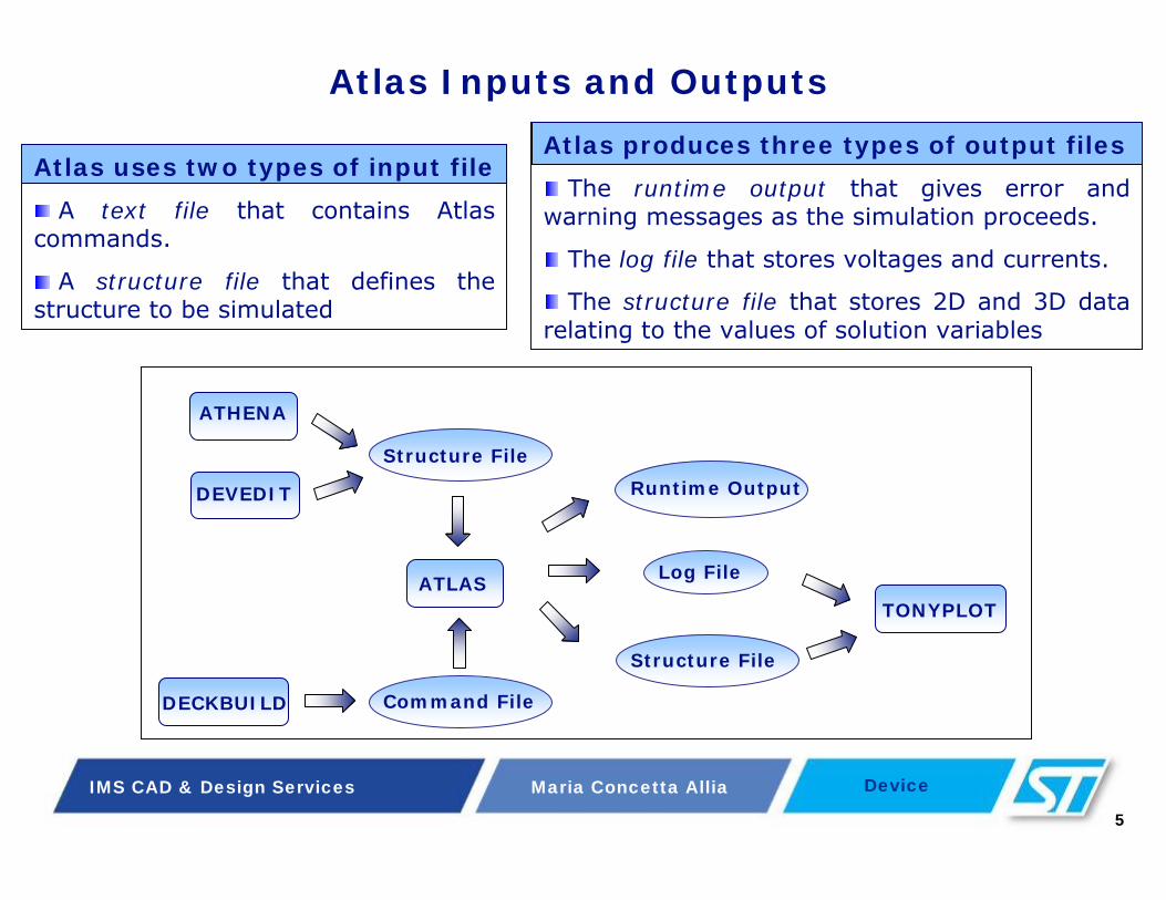
Atlas Inputs and Outputs
ATHENA
Structure File
DECKBUILD
DEVEDIT
Command File
ATLASTONYPLOT
Structure File
Runtime Output
Log File
Atlas uses two types of input file
A text file that contains Atlas commands.
A structure file that defines the structure to be simulated
Atlas produces three types of output files
The runtime output that gives error and warning messages as the simulation proceeds.
The log file that stores voltages and currents.
The structure file that stores 2D and 3D data relating to the values of solution variables

6
Maria Concetta Allia DeviceIMS CAD & Design Services
Atlas input structure
There is a trade-off between the requirements of accuracy and numerical efficiency
The physical structure built by Athena is used as input by Atlas to predict its electrical behavior. The grid of the input structure is crucial for the device simulation.
Accuracy requires a fine grid
Numerical efficiency is greater when fewer grid points are used
The most efficient way to work is to allocate a fine grid only in critical areas and a coarser grid elsewhere. Most critical areas tend to coincide with reverse biased metallurgical junctions.
Typical critical areas
Transverse electric field under the MOSFET gate
Areas of considerable recombination effects
Areas of high impact ionization

7
Maria Concetta Allia DeviceIMS CAD & Design Services
Question 1
An Atlas input file is:
a) a text file that contains Atlas commands
b) a log file that stores voltages and currents
c) a structure file that contains Atlas commands

8
Maria Concetta Allia DeviceIMS CAD & Design Services
Devedit
Usually, a grid that is appropriate for process simulation is not always appropriate for device simulation.
To remesh the process simulation output for device simulation, the structure editing end griding tool Devedit can be used.
The Standard Structure File can be read into Devedit.
The mesh contained into the file can be replaced using the meshbuild algorithm.
The mesh can be refined by setting parameters that describe critical areas or by simply pointing to the areas that require refinement.
Before remeshing
After remeshing8000 nodes
3500 nodes

9
Maria Concetta Allia DeviceIMS CAD & Design Services
Remeshing
When remeshing a structure for device simulation
Ensure adequate mesh density in high field areas
Avoid abrupt discontinuities in mesh density
Avoid, or at least minimize, the number of obtuse triangles
Avoid, or at least minimize, the number of long and thin triangles
Atlas sets some limits on the maximum number of grid nodes
2D Atlas simulations have a maximum node limit of 20,000. This limit is high enough for simulations of conventional devices.
For most 2D simulations, you can obtain accurate results with somewhere between 6,000 and 10,000 node points properly located in the structure.

10
Maria Concetta Allia DeviceIMS CAD & Design Services
When remeshing a structure for device simulation, ensure:
a) an adequate number of obtuse triangles
b) a number of nodes greater than 20,000
c) an adequate mesh density in critical areas
Question 2
11
Maria Concetta Allia DeviceIMS CAD & Design Services
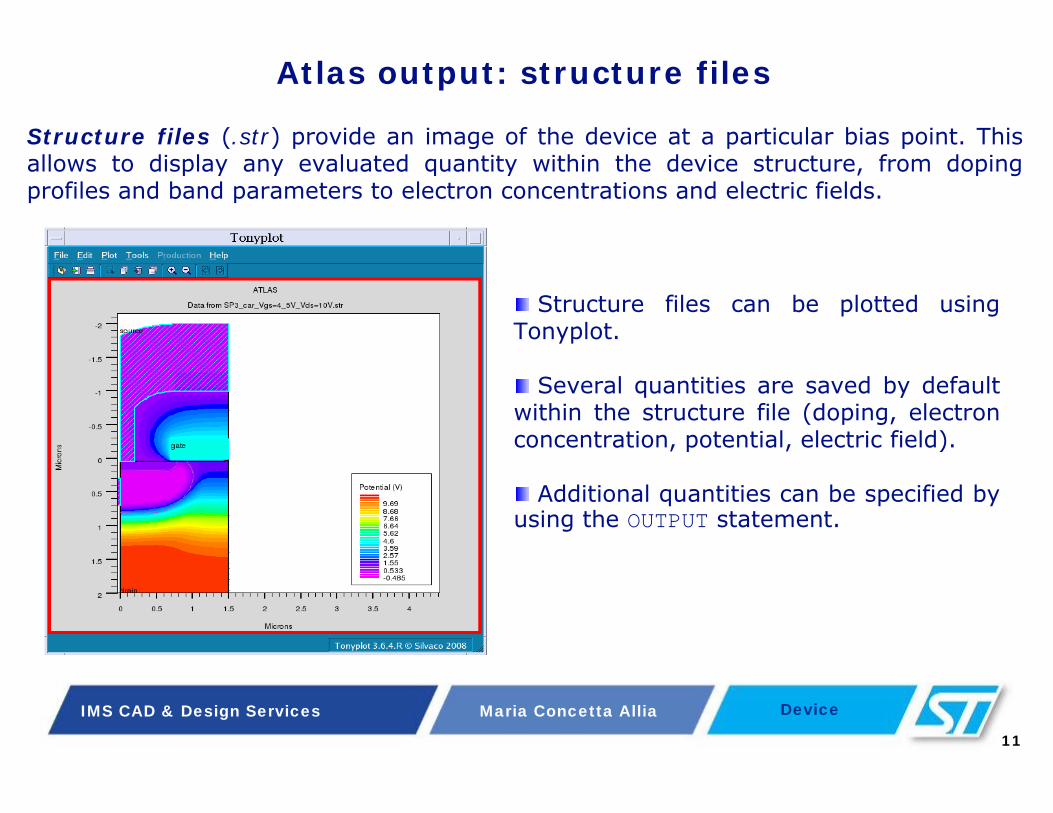
Atlas output: structure files
Structure files (.str) provide an image of the device at a particular bias point. This allows to display any evaluated quantity within the device structure, from doping profiles and band parameters to electron concentrations and electric fields.
Structure files can be plotted using Tonyplot.
Several quantities are saved by default within the structure file (doping, electron concentration, potential, electric field).
Additional quantities can be specified by using the OUTPUT statement.

12
Maria Concetta Allia DeviceIMS CAD & Design Services
Atlas output: log files
Log files (.log) store the terminal characteristics calculated by Atlas. These are current and voltages at electrodes in DC simulations. In transient simulations, the time is stored. In AC simulations, the small signal frequency, the conductances and capacitances are saved.
Log files can be plotted using Tonyplot.
The statement LOG OUTF=<FILENAME> is used to open a log file. Terminal characteristics from all SOLVE statements after the LOG statement are saved into this file. To not save the terminal characteristics to this file, use the LOG OFFstatement.
A separate log file should be used for each bias sweep. For example, separate log filesare used for each gate bias in a MOS Id/Vdssimulation or for each base current in a bipolar Ic/Vce simulation. These files can be overlaid in Tonyplot.

13
Maria Concetta Allia DeviceIMS CAD & Design Services
Atlas structure output:
a) can be plotted using Tecplot
b) stores currents and voltages at electrodes
c) saves quantities as electron concentration, potential, electric field at a particular bias point
Question 3

14
Maria Concetta Allia DeviceIMS CAD & Design Services
Extract functionThe Extract command (provided within the Deckbuild environment) allows to extract device parameters, operating on the log file or the structure file. To generate the Extract statement:
In the Extraction popup a list of ready-made extract statements is provided
The User defined option allows to generate custom extracts
It is possible to create customized expressions or choose from a number of standard routines provided for the device simulators.
Select Extract → Device… from the Commands menu
It is also possible to take one of the standard expressions andto modify it to suit needs.

15
Maria Concetta Allia DeviceIMS CAD & Design Services
Atlas examples
Atlas examples are a good starting point for creating a device simulation. It is possible to access the examples through Deckbuild:
Click on the Main Control menu
Select Examples:
the examples are divided by technology or technology group
Choose the technology by double clicking over that item:
a list of examples for that technology will appear
Choose a particular example by double clicking over that item in the list:
a text description of the example will appear in the window
Press the Load Example button:
the input command file will be loaded into Deckbuild
Press the Run button to run the example
16
Maria Concetta Allia DeviceIMS CAD & Design Services
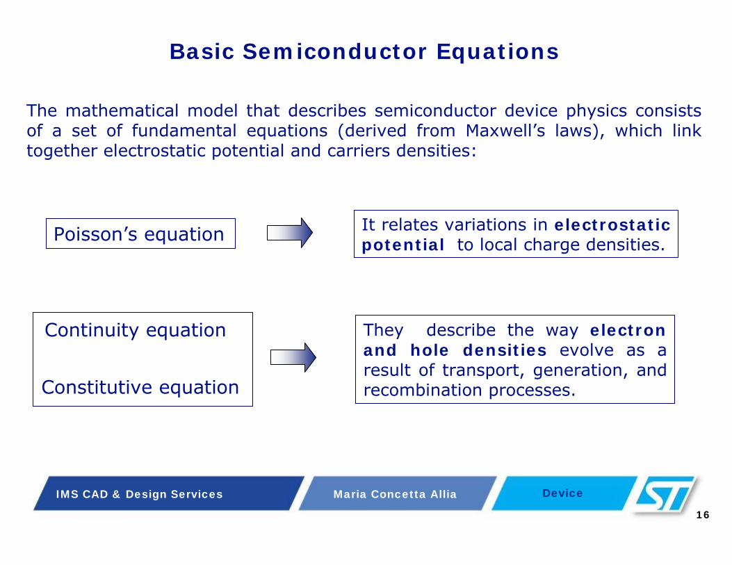
Basic Semiconductor Equations
The mathematical model that describes semiconductor device physics consists of a set of fundamental equations (derived from Maxwell’s laws), which link together electrostatic potential and carriers densities:
It relates variations in electrostatic potential to local charge densities.
They describe the way electron and hole densities evolve as a result of transport, generation, and recombination processes.
Poisson’s equation
Continuity equation
Constitutive equation

17
Maria Concetta Allia DeviceIMS CAD & Design Services
It relates variations in electrostatic potential to space charge densities:
where:
ψ is the electrostatic potentialε is the local permittivityρ is the local space charge density
The local space charge density is the sum of contributions from all mobile and fixed charges, including electrons, holes, and ionized impurities.
ρψε −=∇ ) (div
The electric field is obtained from the gradient of the potential:
ψ∇= -E
Poisson’s equation

18
Maria Concetta Allia DeviceIMS CAD & Design Services
The continuity equations for electrons and holes are defined by:
where:
ppp
nnn
RGJdivqt
p
RGJdivqt
n
−−−−====++++∂∂∂∂∂∂∂∂
−−−−====−−−−∂∂∂∂∂∂∂∂
1
1
Carrier continuity equation
n and p are the electron and hole concentration
and are the electron and hole current densities
and are the generation rates for electrons and holes
and are the recombination rates for electrons and holes
q is the the magnitude of electron charge.
pn JJ
pn GG
pn RR
It is sufficient in some cases solving only one carrier continuity equation.

19
Maria Concetta Allia DeviceIMS CAD & Design Services
The current density equations, usually obtained by applying approximationsto the Boltzmann Transport Equation, define the Transport Model.
The simplest model of constitutive equations defines the Drift-Diffusion Model
where:
and are the electron and hole mobilities
are the Einstein relationships
is the Electric Field
nqDEqnJ nnnn ∇∇∇∇++++====
µµµµ
ψ-E ∇=
pn µµ
pLB
pnLB
n qTKD
qTKD µµ == ,
pqDEqpJ pppp ∇∇∇∇−−−−====
µµµµ
Constitutive equations
Secondary equations are needed to specify physical models for Jn , Jp , Gn , Rn , Gp , Rp
Hydrodynamic Model
Energy Balance Model
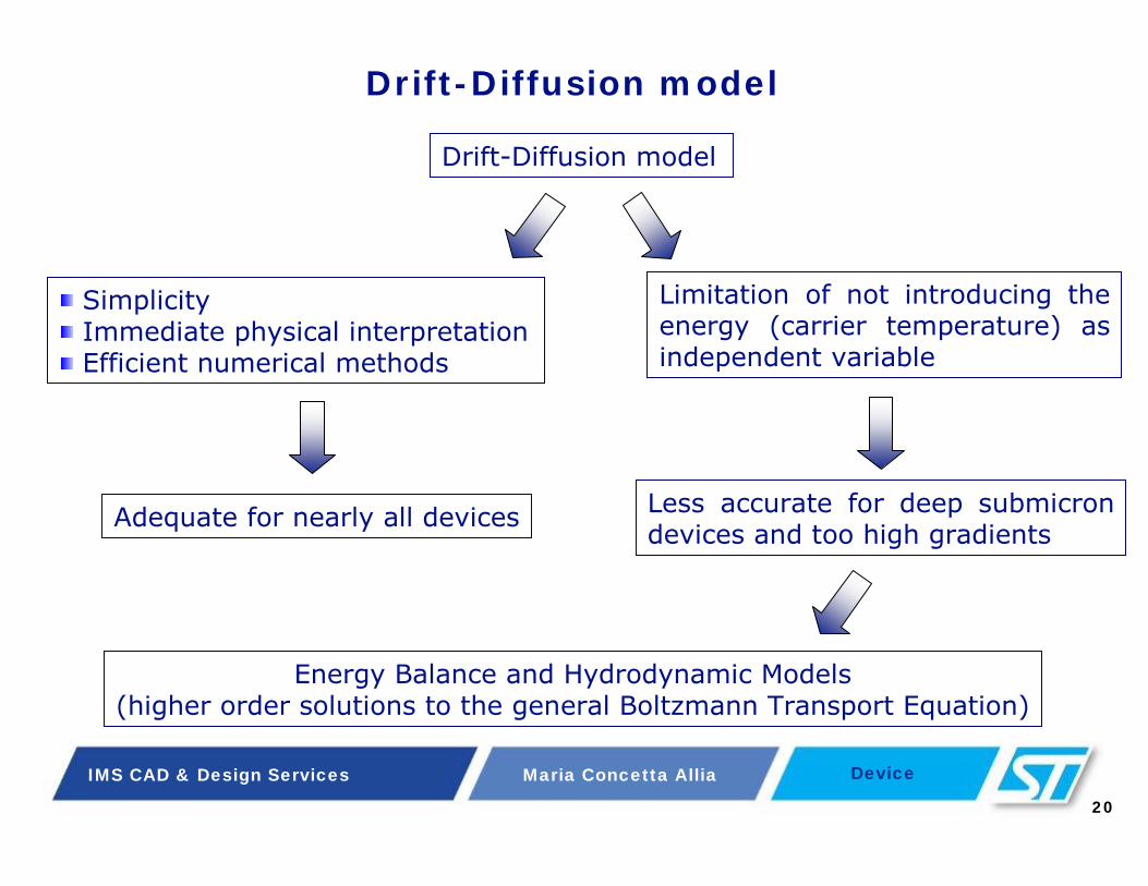
Drift-Diffusion Model
20
Maria Concetta Allia DeviceIMS CAD & Design Services
Energy Balance and Hydrodynamic Models(higher order solutions to the general Boltzmann Transport Equation)
SimplicityImmediate physical interpretationEfficient numerical methods
Limitation of not introducing the energy (carrier temperature) as independent variable
Adequate for nearly all devices Less accurate for deep submicron devices and too high gradients
Drift-Diffusion model
Drift-Diffusion model

21
Maria Concetta Allia DeviceIMS CAD & Design Services
Question 4
The simplest transport model implemented in the device simulators is:
a) the Hydrodynamic model
b) the Energy Balance model
c) the Drift-Diffusion model

22
Maria Concetta Allia DeviceIMS CAD & Design Services
Physical Models
Physical models implemented in Atlas can be grouped into five classes
Mobility
Recombination
Carrier statistics
Impact ionization
Tunneling
All models with exception of impact ionization are specified on the MODELSstatement. Impact ionization is specified in the IMPACT statement.
Next slides will give a summary description and recommendations on the use of the most important models.

23
Maria Concetta Allia DeviceIMS CAD & Design Services
Mobility model
Electrons and holes are accelerated by electric fields, but lose momentum as a result of scattering processes, which includes:
Lattice vibrations (phonons)Impurity ionsOther carriersMaterial imperfections (surface roughness, …)
Complete model including N, T, E// and E effects. Good for non-planar devices.
cvtLombardi (CVT) Model
It is a doping versus mobility table valid for 300K only.conmobConcentration Dependent
Caughey - Thomas formula. Tuned for 77-450K.analyticConcentration andTemperature Dependent
Important when carrier concentration is high (e.g., forward bias power devices).ccsmobCarrier-Carrier Scattering
NotesSyntaxModel
Includes N, E// and E effects. Only for 300K.yamaguchiYamaguchi Model
Required to model any type of velocity saturation effect.fldmobParallel Electric Field Dependence

24
Maria Concetta Allia DeviceIMS CAD & Design Services
Carrier generation-recombination is the process through which the semiconductor material attempts to return to equilibrium after being disturbed from it.
Uses fixed minority carrier lifetimes.It Should be used in most simulations.srhShockley-Read-Hall
Specifies Shockley-Read-Hall recombination using concentration dependent lifetimes.consrh
Concentration Dependent
Specifies Auger recombination.Important at high current densities.augerAuger
NotesSyntaxModel
Phonon transitions
Photon transitions
Auger transitions
Surface recombination
Impact ionization
Tunneling
Processes responsible for generation-recombination
Carrier Generation-recombination model
25
Maria Concetta Allia DeviceIMS CAD & Design Services
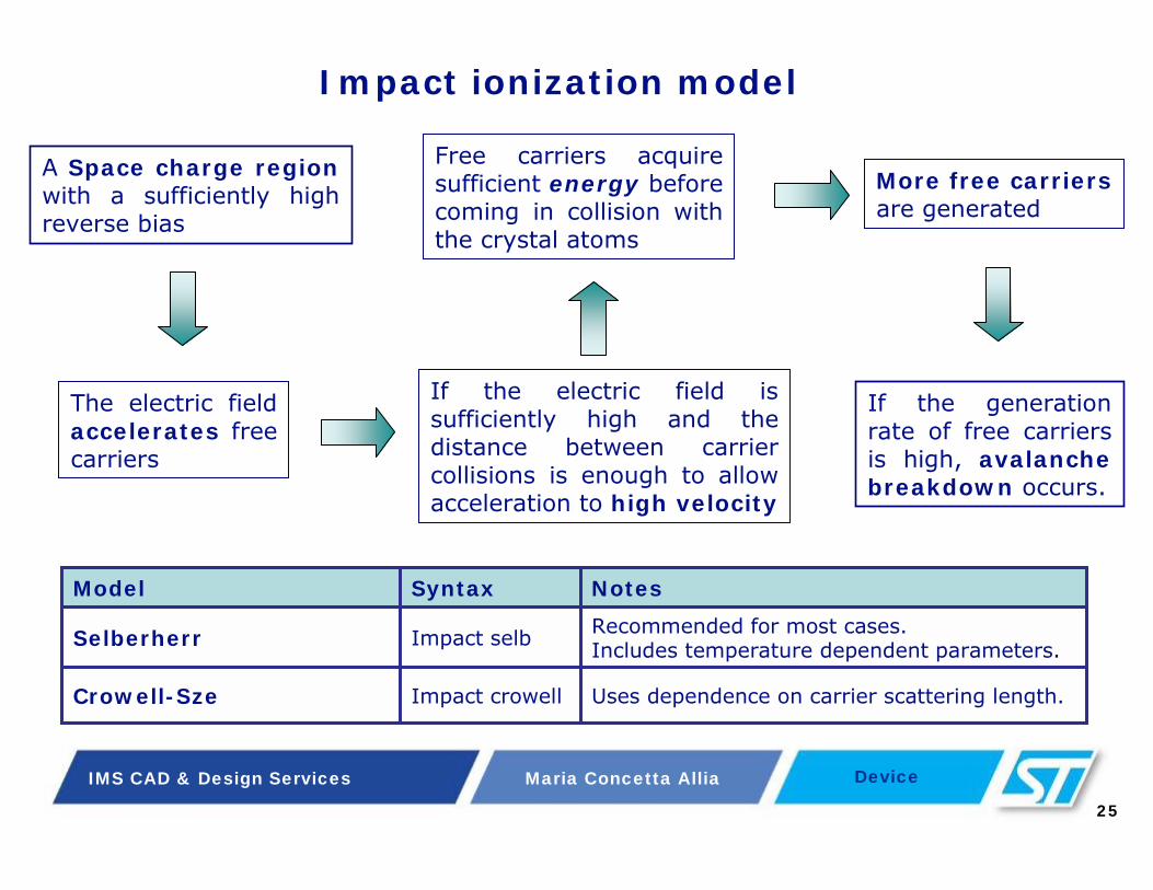
A Space charge regionwith a sufficiently high reverse bias
Recommended for most cases. Includes temperature dependent parameters. Impact selbSelberherr
Uses dependence on carrier scattering length.Impact crowellCrowell-Sze
NotesSyntaxModel
If the electric field is sufficiently high and the distance between carrier collisions is enough to allow acceleration to high velocity
Impact ionization model
If the generation rate of free carriers is high, avalanche breakdown occurs.
The electric field accelerates free carriers
Free carriers acquire sufficient energy before coming in collision with the crystal atoms
More free carriersare generated

26
Maria Concetta Allia DeviceIMS CAD & Design Services
Model Macros
MODELS MOS PRINT
Enables the CVT, SRH, and FERMI models
Atlas provides an easy method for selecting the correct models for various technologies. The MOS and BIPOLAR parameters for the MODELS statement configure a basic set of mobility, recombination, carrier statistics, and tunneling models for MOSFET and BIPOLAR devices.
The print option in the MODELS statement displays the details of material parameters and mobility models at the start of the run-time output.
MODELS BIPOLAR PRINT
Enables the CONMOB, FLDMOB, CONSRH, AUGER, and BGN models

27
Maria Concetta Allia DeviceIMS CAD & Design Services
Models specification in Atlas is:
a) not necessary for impact ionization
b) possible only for bipolar device
c) possible through MODELS and IMPACT statements
Question 5
28
Maria Concetta Allia DeviceIMS CAD & Design Services
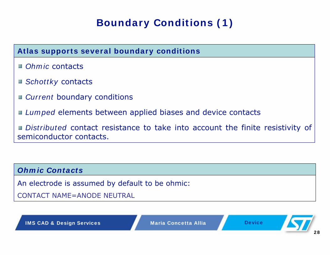
Boundary Conditions (1)
Ohmic Contacts
An electrode is assumed by default to be ohmic:
CONTACT NAME=ANODE NEUTRAL
Atlas supports several boundary conditions
Ohmic contacts
Schottky contacts
Current boundary conditions
Lumped elements between applied biases and device contacts
Distributed contact resistance to take into account the finite resistivity of semiconductor contacts.

29
Maria Concetta Allia DeviceIMS CAD & Design Services
Boundary Conditions (2)
Current boundary conditions
Calculation of current boundary conditions is activated by the CURRENT parameter in the CONTACT statement:
CONTACT NAME=BASE CURRENT
Current controlled electrodes are useful when the current is highly sensitive to voltage or is a multi-valued function of voltage (post-breakdown and snap-back).
Schottky Contacts
To set a Schottky contact, specify a workfunction (eV) using the WORKFUN parameter of the CONTACT statement:
CONTACT NAME=BODY WORKFUN=4.94
In practice, the workfunction is defined as
WORKFUN= AFFINITY+ΦB
where ΦB is the barrier height at the metal-semiconductor interface in eV. For example, if the Schottky contact is aluminum with a workfunction difference to the silicon of 4.2eV and a barrier height of 0.7eV, then WORKFUN=4.9

30
Maria Concetta Allia DeviceIMS CAD & Design Services
Boundary Conditions (3)
External Resistor, Capacitors, Inductors
Resistance, capacitance and inductance connected to an electrode can be specified using the RESISTANCE, CAPACITANCEand INDUCTANCE parameters in the CONTACT statement:
CONTACT NAME=DRAIN CAPACITANCE=20e-12
Since contact materials have finite resistivities, the electrostatic potential is not always uniform along the metal-semiconductor surface. To account for this effect, a distributedcontact resistance can be associated with any electrode using the CON.RESIST parameter:
CONTACT NAME=SOURCE CON.RESITANCE=0.01
H· µminductance
Ω·µmresistance
F/µmcapacitance
Ω·cm2con.resistance
UnitsParameter
Floating Contacts
To specify a floating contact place a very large resistor at the electrode:
CONTACT NAME=SOURCE RESISTANCE=1e14
31
Maria Concetta Allia DeviceIMS CAD & Design Services
For what concerns boundary conditions:
a) it’s possible to define only ohmic contacts
b) it’s possible to switch to current control
c) it’s not possible to specify floating contacts
Question 6

32
Maria Concetta Allia DeviceIMS CAD & Design Services
Numerical Methods (1)
Different numerical methods can be used for calculating the solutions to semiconductor device problems.
Different combinations of models require Atlas to solve up to six coupled, non-linear, partial differential equations (PDEs).Atlas solves the equations
calculating the values of unknowns on a mesh of points within the device.
The set of PDEs, the mesh and the discretization procedure determine the non-linear algebraic problemthat must be solved.
A discretization procedure converts the original continuous model to a discrete algebraic system that has approximately the same behavior.

33
Maria Concetta Allia DeviceIMS CAD & Design Services
Numerical Methods (2)
The non-linear iteration procedure starts from an initial guess and uses an iterative procedure that refines successive estimates of the solution.
Iteration continues until the corrections are small enough to satisfy convergence criteria, or until it is clear that the procedure is not going to converge.
When a solution fails to converge, a user normally tries a different grid, a different initial guess strategy, or a different non-linear iteration technique.
There are three types of solution techniques: Gummel, Newton and Block.
Numerical methods are given in the METHOD statements of the input file.
If more then one method is specified in the same METHOD statement, each solution method will be applied in succession until convergence is obtained.
The order that the solution methods will be applied is Gummel then Block then Newton. If no solution methods are specified Newton is applied by default.
34
Maria Concetta Allia DeviceIMS CAD & Design Services
Gummel and Block Method
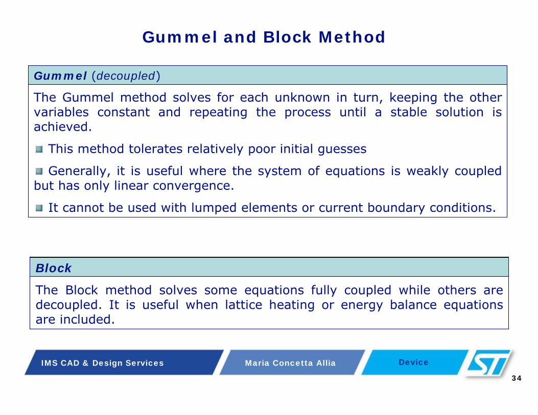
Gummel (decoupled)
The Gummel method solves for each unknown in turn, keeping the other variables constant and repeating the process until a stable solution is achieved.
This method tolerates relatively poor initial guesses
Generally, it is useful where the system of equations is weakly coupled but has only linear convergence.
It cannot be used with lumped elements or current boundary conditions.
Block
The Block method solves some equations fully coupled while others are decoupled. It is useful when lattice heating or energy balance equations are included.
35
Maria Concetta Allia DeviceIMS CAD & Design Services
Newton Method
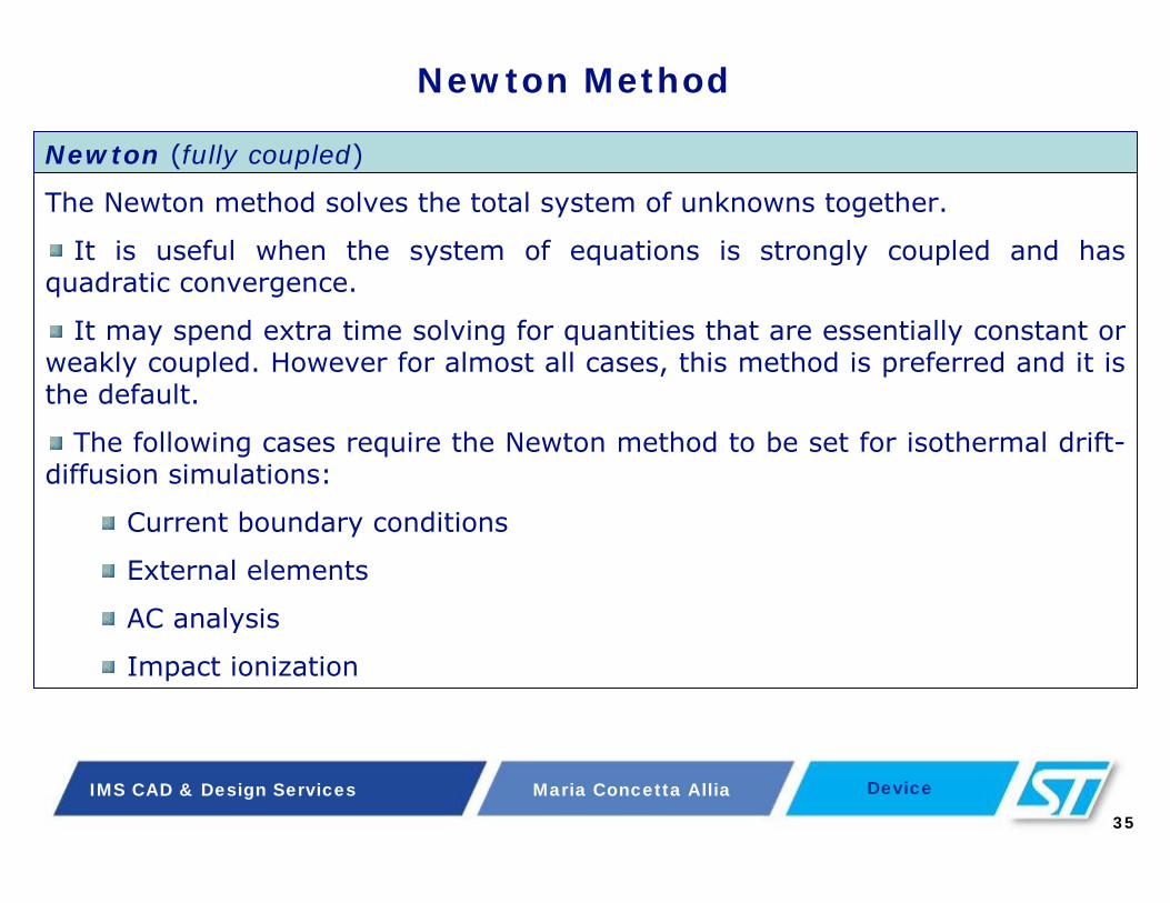
Newton (fully coupled)
The Newton method solves the total system of unknowns together.
It is useful when the system of equations is strongly coupled and has quadratic convergence.
It may spend extra time solving for quantities that are essentially constant or weakly coupled. However for almost all cases, this method is preferred and it is the default.
The following cases require the Newton method to be set for isothermal drift-diffusion simulations:
Current boundary conditions
External elements
AC analysis
Impact ionization

36
Maria Concetta Allia DeviceIMS CAD & Design Services
In Atlas three types of numerical methods are implemented:
a) Shockley, Read, Hall
b) Gummel, Newton, Crowell
c) Block, Newton, Gummel
Question 7
37
Maria Concetta Allia DeviceIMS CAD & Design Services
Obtaining Solutions
Solution statements
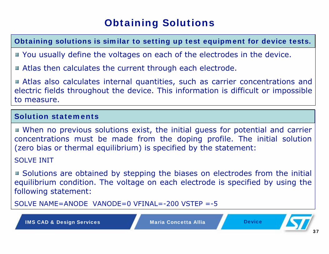
When no previous solutions exist, the initial guess for potential and carrier concentrations must be made from the doping profile. The initial solution (zero bias or thermal equilibrium) is specified by the statement:
SOLVE INIT
Solutions are obtained by stepping the biases on electrodes from the initial equilibrium condition. The voltage on each electrode is specified by using the following statement:
SOLVE NAME=ANODE VANODE=0 VFINAL=-200 VSTEP =-5
Obtaining solutions is similar to setting up test equipment for device tests.
You usually define the voltages on each of the electrodes in the device.
Atlas then calculates the current through each electrode.
Atlas also calculates internal quantities, such as carrier concentrations and electric fields throughout the device. This information is difficult or impossible to measure.
38
Maria Concetta Allia DeviceIMS CAD & Design Services
Atlas Statements
CONTACT
LOAD
SAVE
SOLVE
METHOD3. Numerical Method Selection
ELECTRODE
StatementsGroup
LOG
4. Solution Specification
MODELS2. Models specification
MESH
1. Structure Specification
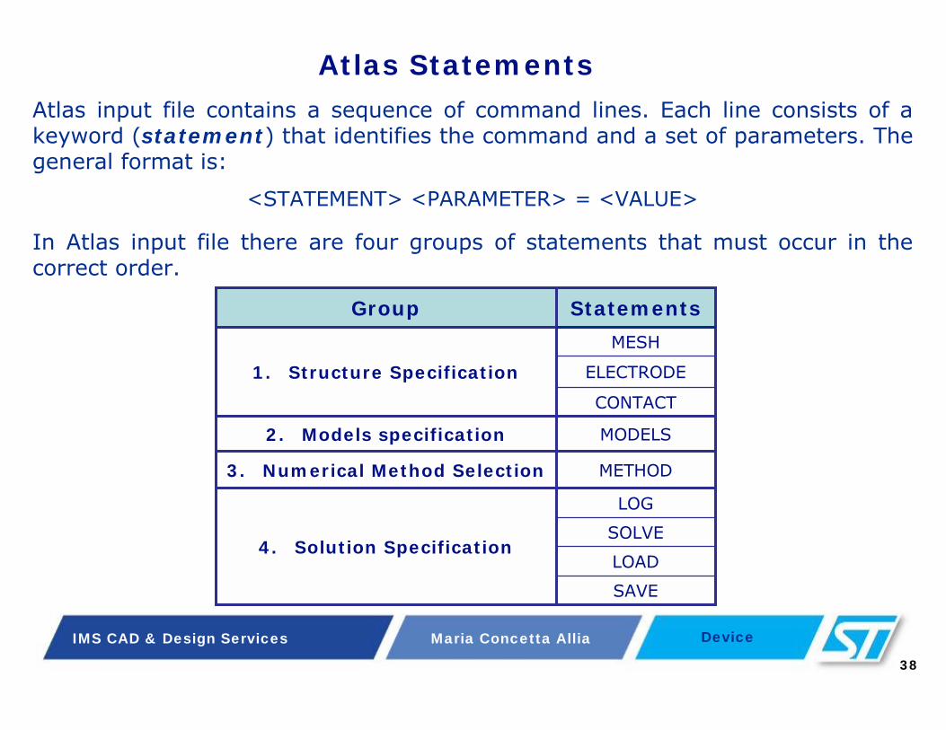
Atlas input file contains a sequence of command lines. Each line consists of a keyword (statement) that identifies the command and a set of parameters. The general format is:
<STATEMENT> <PARAMETER> = <VALUE>
In Atlas input file there are four groups of statements that must occur in the correct order.

39
Maria Concetta Allia DeviceIMS CAD & Design Services
Running Atlas inside DeckbuildWhen Atlas is the active simulator in Deckbuild, the Commands menu is configured for Atlas statements and can help to create the input file.
To specify the structure
To specify the models
To define numerical methodsand solution conditions
To define Extract functionTo access Atlas coefficients file

40
Maria Concetta Allia DeviceIMS CAD & Design Services
Diode breakdown simulation
Basic operations to create the input file
Loading the diode structure
Specifying the electrodes (anode and cathode)
Selecting the bipolar models and the impact ionization model
Specifying the numerical method
Reverse biasing the diode to obtain the breakdown curve
Saving the log and the structure files
The following section provides a typical example of device simulation. The input file of a breakdown simulation of a simple pn diode is generated by using Deckbuild interface.

41
Maria Concetta Allia DeviceIMS CAD & Design Services
Structure Specification: the MESH statementA 2D or 3D structure created by Athena or Devedit can be read into Atlas using the statement MESH INFILE, which loads in mesh, geometry, electrode positions, and doping of the structure. To generate the MESH statement:
Select Structure → Mesh… from the Commands menu
Select the Read from file button and write the name of the structure you want to load in.
Press the Write button and the corresponding command line will appear in the Deckbuild Text Subwindow.

42
Maria Concetta Allia DeviceIMS CAD & Design Services
To define the electrodes an ELECTRODE statement has to be generated:
Structure Specification: the ELECTRODE statement
Electrodes must be specified in the same sequential order of Devedit or Athena.
To add an electrode press the Add electrodebutton and select a name. The name will appear in the scrolling list.
Repeat this procedure once per electrode in the device.
Before writing the electrode information into the input file, assign boundary conditions to the electrode.
Select Structure → Electrode… from the Commands menu
43
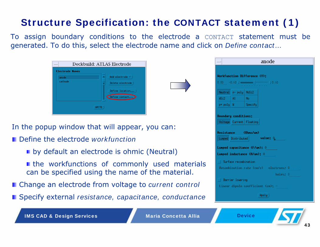
Maria Concetta Allia DeviceIMS CAD & Design Services
Structure Specification: the CONTACT statement (1)To assign boundary conditions to the electrode a CONTACT statement must be generated. To do this, select the electrode name and click on Define contact…
In the popup window that will appear, you can:
Define the electrode workfunction
by default an electrode is ohmic (Neutral)
the workfunctions of commonly used materials can be specified using the name of the material.
Change an electrode from voltage to current control
Specify external resistance, capacitance, conductance

44
Maria Concetta Allia DeviceIMS CAD & Design Services
Structure Specification: the CONTACT statement (2)
The command lines corresponding to ELECTRODE and CONTACT statement will appear on the Deckbuild Text window.
Select the cathode electrode name and set the boundary conditions in the same way.
Finally, press the Write button.

45
Maria Concetta Allia DeviceIMS CAD & Design Services
Models Specification
Deckbuild provides an easy method for selecting the correct models for the different technologies. Deckbuild window for setting Atlas models shows two fields:
Category, which allows to select the class of models.
Defaults, which allows to configure a basic set of models for Mosfet and Bipolar devices.
If MOS is chosen in the Defaults field, the models suitable for Mosfet devices will be selected in each Category.
If Bipolar is chosen in the Defaults field, the models suitable for Bipolar devices will be selected in each Category.
Select Models → Models… from the Commands menu
All models with exception of impact ionization are specified on the MODELS statement. Impact ionization is specified in the IMPACT statement. To generate these statements:

46
Maria Concetta Allia DeviceIMS CAD & Design Services
Models for Bipolar devices (1)Choosing Bipolar for simulating diode behavior, the corresponding models are selected.
Recombination
Mobility Statistics

47
Maria Concetta Allia DeviceIMS CAD & Design Services
Models for Bipolar devices (2)
Pressing the Write button, the MODELS statement with the appropriate bipolar models is written in the Deckbuild window.
Recombination
auger : Auger recombination
consrh : Shockley-Read-Hall recombination with concentration dependent lifetimes
Mobility
conmob : concentration dependent mobility
fldmob : field dependent mobility
Statistics
boltzmann : Boltzmann carrier statistics
bgn : band gap narrowing

48
Maria Concetta Allia DeviceIMS CAD & Design Services
Models for Bipolar devices (3)
bipolar: enables the conmob, fldmob, consrh, auger and bgn models.
temperature: specifies the lattice temperature in Kelvin
print: displays the details of material parameters and mobility models at the start of the run-time output.
The same models can be selected writing the bipolar parameter in the MODELSstatement.

49
Maria Concetta Allia DeviceIMS CAD & Design Services
Impact Ionization Model
By default nothing is selected for the Impact ionization model. Click on Selberherr to enable the corresponding model. The IMPACT statement is generated in the input file.
Impact ionization

50
Maria Concetta Allia DeviceIMS CAD & Design Services
In order to perform a breakdown simulation it is crucial to set:
a) the cvt mobility model
b) the impact ionization model
c) current boundary conditions
Question 8

51
Maria Concetta Allia DeviceIMS CAD & Design Services
Numerical Method Selection (1)
Different numerical methods can be used to calculate the solutions of semiconductor device problems. Numerical methods are given in the METHOD statement:
Select Solutions → Method… from the Commands menu
Select one of the three available methods:
Newton
Gummel
Block
Set the maximum number of iterations (default=25).
Allow reducing bias steps if solution diverges.
Press the Write button to write the method command line in the input file.

52
Maria Concetta Allia DeviceIMS CAD & Design Services
Numerical Method Selection (2)
itlimit: specifies the maximum number of allowed iteration (default=25).
trap: specifies that the electrode bias steps are reduced by the multiplication factor atrap, if a solution starts to diverge.
atrap: specifies the multiplication factor that reduces the electrode bias steps when the solution diverges (default=0.5).
maxtrap: specifies the number of times the trap procedure will be repeated in case of divergence (default=4). A value of maxtrap=10 is recommended for breakdown simulation.
Pressing the Write button the METHOD command line is written in the input file

53
Maria Concetta Allia DeviceIMS CAD & Design Services
Numerical Method Selection (3)
* Note that it is not necessary to write the parameters with the default values. Therefore itlimit=25 and atrap=0.5 can be omitted. You need to introduce them if you want to modify their default values.
Deckbuild does not support all possible Atlas syntax. Therefore not all the available parameters can be inserted in the input file by using Deckbuild interface.
The command lines generated in the Deckbuild Text window can be easily modified by hand. Parameters can be added and their values modified just typing on the window.
For all breakdown simulation it is recommended:
to increase the maxtrap value to 10
to add the climit parameter to the method statement and to reduce its value to 1e-4 (default=1e4)

54
Maria Concetta Allia DeviceIMS CAD & Design Services
Question 9
The parameter trap in the METHOD statement:
a)places donor traps at oxide/silicon interface
b)reduces the bias step to improve convergence
c) activates the trap numerical method

55
Maria Concetta Allia DeviceIMS CAD & Design Services
To add a new row, click the right mouse button in the worksheet and select Add new row.
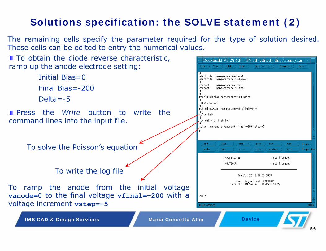
Solutions specification: the SOLVE statement (1)
To generate a SOLVE statement select Solutions → Solve… in the Commands menu.
In the first cell, to edit the electrode name press the right mouse button and select the desired name.
The second cell specifies if the electrode is voltage (V), current (I) or charge (Q) controlled.
The third cell specifies whether the SOLVE statement is to be a single DC solve (CONST), a swept DC variable (VAR1), a stepped DC variable (VAR2), or a transient solution (PULSE).
56
Maria Concetta Allia DeviceIMS CAD & Design Services
The remaining cells specify the parameter required for the type of solution desired. These cells can be edited to entry the numerical values.
To obtain the diode reverse characteristic, ramp up the anode electrode setting:
Initial Bias=0
Final Bias=-200
Delta=-5
Press the Write button to write the command lines into the input file.
To solve the Poisson’s equation
To write the log file
To ramp the anode from the initial voltage vanode=0 to the final voltage vfinal=-200 with a voltage increment vstep=-5
Solutions specification: the SOLVE statement (2)
57
Maria Concetta Allia DeviceIMS CAD & Design Services
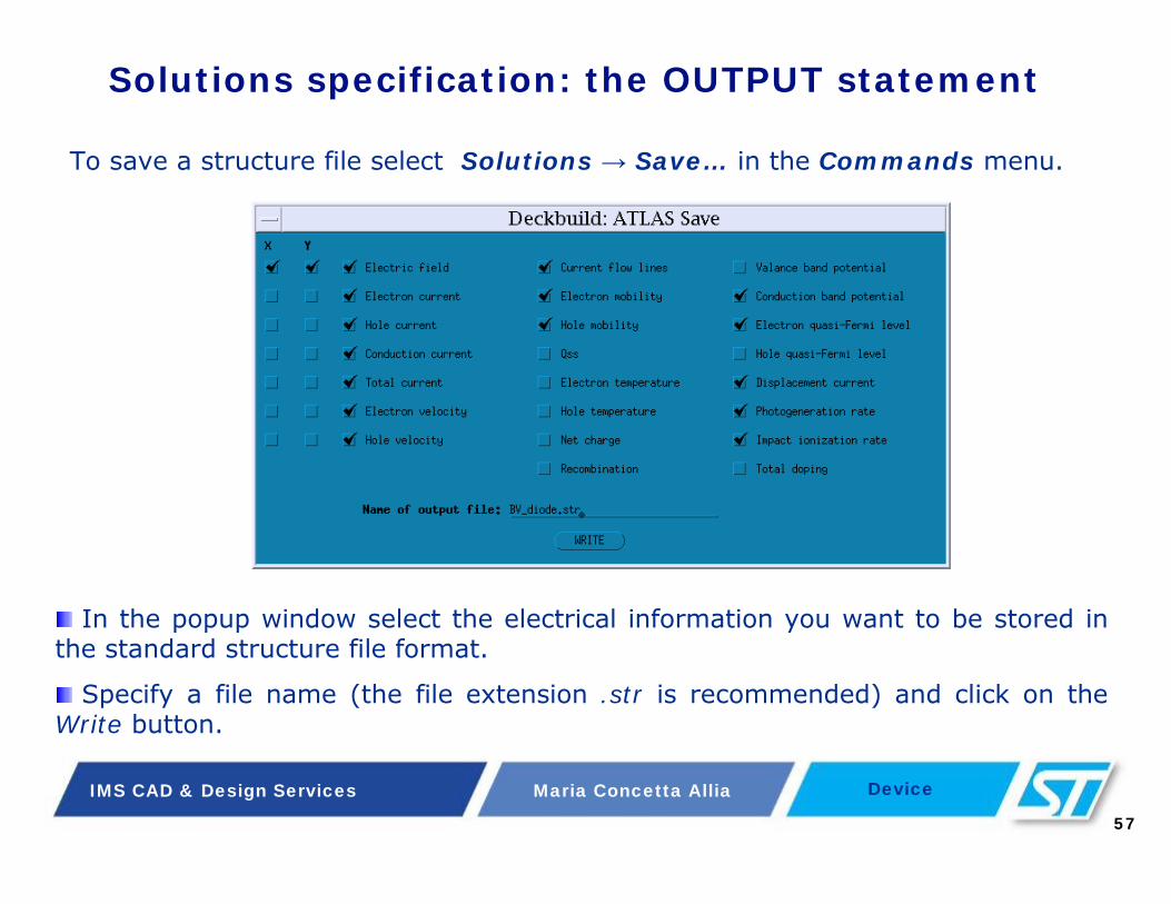
To save a structure file select Solutions → Save… in the Commands menu.
In the popup window select the electrical information you want to be stored in the standard structure file format.
Specify a file name (the file extension .str is recommended) and click on the Write button.
Solutions specification: the OUTPUT statement

58
Maria Concetta Allia DeviceIMS CAD & Design Services
Pressing the Write button, two statements appear in the input file:
OUTPUT allows to specify electrical quantities to be stored in the structure file and subsequently displayed using Tonyplot.
SAVE OUTF saves in a structure file all electrical data specified in the OUTPUTstatement. If a solve statement has preceded a save statement the data from the last solution is stored.
Solutions specification: the SAVE statement

59
Maria Concetta Allia DeviceIMS CAD & Design Services
The OUTPUT statement:
a) saves an output structure file
b) loads a previously saved structure file
c) allows to specify the electrical information to be stored in the structure file
Question 10

60
Maria Concetta Allia DeviceIMS CAD & Design Services
Obtaining Solutions around the breakdown voltageObtaining solutions around the breakdown voltage requires special care. The breakdown curve is flat up to a voltage very close to breakdown and then almost vertical. The current change by orders of magnitude for very small bias increments produces some convergence problems. Consider the following statement:
SOLVE NAME=ANODE VANODE=0 VFINAL=-200 VSTEP=-5
If the breakdown occurs at 78V, there are no solutions for voltages greater than 78V.
Atlas is trying to ramp to 200V, so it is inevitable it will fail to converge at some point.
Bias step reduction will take place due to the trap parameter.
Atlas will continually try to increase the drain voltage until it reaches the limit set by the maxtrap parameter.
Typically, to see the breakdown point the current should increase by two orders of magnitude in a small voltage increment.
If the current does not reach a sufficiently high level, instead of reducing the voltage step, increase the maxtrap value.

61
Maria Concetta Allia DeviceIMS CAD & Design Services
Run-time output (1)
Not all errors are fatal because Deckbuild tries to interpret the file and continue. This may cause a statement to be ignored, leading to unexpected results.
During the running simulation it is recommended to check the run-time output to intercept any errors or warnings.
During SOLVE statements, the error numbers of each equation at each iteration are displayed. It can provide important insights in the case of convergence problems.
Run-time output is provided at the bottom of the Deckbuild Window. Errors occurring during the simulation run will be displayed in this output.

62
Maria Concetta Allia DeviceIMS CAD & Design Services
Run-time output (2)
proj psi n p psi n p direct x x x rhs rhs rhs
i j m -5.00* -5.00* -5.00* -26.0* -17.3* -17.3*---------------------------------------------------------------------------
1 N 0.677 1.090 1.031 -16.99 -12.09 -5.6692 N 0.080 0.145 1.514 -17.64 -12.99 -6.0443 N -0.838 -0.000 0.802 -28.7* -15.36 -7.6724 N -2.318 -0.901 -0.589 -29.8* -18.4* -10.935 N -5.62* -3.304 -4.209 -29.8* -23.8* -17.4*
Electrode Va(V) Jn(A/um) Jp(A/um) Jc(A/um) Jt(A/um)=============================================anode -1.000e+01 -3.224e-18 -1.506e-13 -1.506e-13 -1.506e-13cathode 0.000e+00 1.210e-13 2.951e-14 1.506e-13 1.506e-13Total 2.220e-19
The output can be interpreted as follows:
iterationnumbers
solutionmethod
XNORM and RHSNORM errors
error values
This error has met its tolerance
voltage at the contact surface
electron, hole, conduction, and total currents
tolerance values
N = NewtonG = GummelB = Block

63
Maria Concetta Allia DeviceIMS CAD & Design Services
Displaying the results
STRUCTURE FILELOG FILE
The electric field at breakdown is displayed. The higher electric field regions (in red) show where the breakdown occurs.
A typical breakdown curve is showed (BV=78V). The cathode current is displayed as function of the anode voltage.