Managing Connector and Cable Assembly Performance … · Managing Connector and Cable Assembly...
17
Managing Connector and Cable Assembly Performance for USB SuperSpeed, Revision 1.0 Whitepaper Managing Connector and Cable Assembly Performance for USB SuperSpeed Revision 1.0 February 1, 2013 Abstract USB 3.0 connector and cable assembly performance can have a significant impact on USB SuperSpeed operation and needs to be properly managed. This document discusses how to manage the USB SuperSpeed connector and cable assembly performance, particularly signal integrity impairments. Key design considerations or guidelines are described to minimize the signal integrity impairments like reflection, crosstalk and insertion loss. Though the focus is on signal integrity, some discussions are given to EMI/RFI and mechanical aspects also. Following the guidelines provided in this document by connector and cable assembly makers will ensure a healthy eco-system for USB 3.0 and a good user experience. Introduction USB SuperSpeed, operating at 5 Gb/s, offers 10x increase of bandwidth over USB HighSpeed. However, this bandwidth increase comes with more signal integrity challenges – a 10x increase in signal speed will undoubtedly cause SIGNIFICANT increase in signal loss, reflection and crosstalk. The USB 3.0 connectors and cable assembly are one of the major sources of signal integrity impairments for the USB SuperSpeed link. For example, a USB 3.0 cable assembly may consume a -7.5 dB insertion loss at 2.5 GHz, more than a third of the total link loss budget! Poorly designed and/or manufactured USB 3.0 connectors and cable assemblies may be the root-causes for many system problems. Below are a few examples of USB 3.0 system failures due to poor connectors and cable assemblies that have been reported: Non-interoperability – the same cable assembly works in some system, but is not functional in some other systems. Not able to train to SuperSpeed – instead, the system is trained to operate at USB 2.0 high speed. Radio frequency interference (RFI) – the proximity of USB 3.0 connector and cable assembly makes a wireless device, for example a wireless mouse, cease to work. Unable to function at all.
-
Upload
nguyendung -
Category
Documents
-
view
229 -
download
2
Transcript of Managing Connector and Cable Assembly Performance … · Managing Connector and Cable Assembly...

Managing Connector and Cable Assembly Performance for USB SuperSpeed, Revision 1.0
Whitepaper
Managing Connector and Cable Assembly
Performance for USB SuperSpeed
Revision 1.0
February 1, 2013
Abstract
USB 3.0 connector and cable assembly performance can have a significant impact on USB SuperSpeed
operation and needs to be properly managed. This document discusses how to manage the USB
SuperSpeed connector and cable assembly performance, particularly signal integrity impairments. Key
design considerations or guidelines are described to minimize the signal integrity impairments like
reflection, crosstalk and insertion loss. Though the focus is on signal integrity, some discussions are given
to EMI/RFI and mechanical aspects also. Following the guidelines provided in this document by
connector and cable assembly makers will ensure a healthy eco-system for USB 3.0 and a good user
experience.
Introduction
USB SuperSpeed, operating at 5 Gb/s, offers 10x increase of bandwidth over USB HighSpeed.
However, this bandwidth increase comes with more signal integrity challenges – a 10x increase in signal
speed will undoubtedly cause SIGNIFICANT increase in signal loss, reflection and crosstalk.
The USB 3.0 connectors and cable assembly are one of the major sources of signal integrity impairments
for the USB SuperSpeed link. For example, a USB 3.0 cable assembly may consume a -7.5 dB insertion
loss at 2.5 GHz, more than a third of the total link loss budget! Poorly designed and/or manufactured
USB 3.0 connectors and cable assemblies may be the root-causes for many system problems. Below are a
few examples of USB 3.0 system failures due to poor connectors and cable assemblies that have been
reported:
Non-interoperability – the same cable assembly works in some system, but is not functional in
some other systems.
Not able to train to SuperSpeed – instead, the system is trained to operate at USB 2.0 high speed.
Radio frequency interference (RFI) – the proximity of USB 3.0 connector and cable assembly
makes a wireless device, for example a wireless mouse, cease to work.
Unable to function at all.

Managing Connector and Cable Assembly Performance for USB SuperSpeed, Revision 1.0
The USB 3.0 specification defines the connector and cable assembly performance requirements and there
is a USB-IF compliance program for USB 3.0 connectors and cable assemblies to ensure the eco-system
health. Unfortunately, a recent survey on USB 3.0 cable assemblies available in the retail market shown
that majority of those cable assemblies did not pass the USB 3.0 specification and were not USB-IF
certified. Use of such cable assemblies may cause the system problems described above.
The purpose of this whitepaper is to increase the awareness of the importance of making and use good
USB 3.0 connectors and cable assemblies to ensure pleasant user experience of USB SuperSpeed. It will
start with reviewing the USB 3.0 specification and compliance testing and then discuss the key design
considerations and guidelines to help the cable/connector manufactures manage the connector and cable
assembly performance. Though the focus is on signal integrity, some discussions will be given to
EMI/RFI and mechanical aspects also- there have been recent reports about people encountering RFI and
mechanical issues with the USB 3.0 connectors and cable assemblies.
Connector and Cable Assembly Signal Integrity Requirements
The USB 3.0 Connectors and Cable Assemblies Compliance Document [1] outlines the following main
requirements for SuperSpeed signals:
Mated Connector SuperSpeed Differential Impedance: The impedance range is required to be
from 75 Ohms to 105 Ohms with a 50 ps risetime, measured from the 20% threshold to the 80%
threshold. The risetime is defined at the connector measurement reference plane when the
stimulus just enters the connector under test. The measurement includes the PCB footprint and
wire termination areas.
Figure 1. Mated connector differential impedance requirement
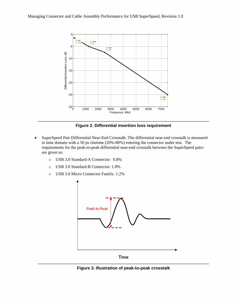
SuperSpeed Differential Insertion: This is for the mated cable assembly. The differential insertion
loss limits are defined by the following vertices: (100 MHz, -1.5 dB), (1.25 GHz, -5.0 dB), (2.5
GHz, -7.5 dB), and (7.5 GHz, -25 dB). The measurement includes the connector footprints at
both ends of the cable assembly, but not the fixture traces. So some calibration structure is
required to remove the fixture loss.
Managing Connector and Cable Assembly Performance for USB SuperSpeed, Revision 1.0
0 1000 2000 3000 4000 5000 6000 7000-30
-25
-20
-15
-10
-5
0
X: 1250
Y: -5
Frequency, MHz
Diffe
ren
tia
l In
se
rtio
n L
oss, d
B
X: 2500
Y: -7.5
X: 7500
Y: -25
X: 2500
Y: -7.5
X: 100
Y: -1.5
Figure 2. Differential insertion loss requirement
SuperSpeed Pair Differential Near-End Crosstalk: The differential near-end crosstalk is measured
in time domain with a 50 ps risetime (20%-80%) entering the connector under test. The
requirements for the peak-to-peak differential near-end crosstalk between the SuperSpeed pairs
are given as:
o USB 3.0 Standard-A Connector: 0.8%
o USB 3.0 Standard-B Connector: 1.8%
o USB 3.0 Micro Connector Family: 1.2%
Figure 3. Illustration of peak-to-peak crosstalk

Managing Connector and Cable Assembly Performance for USB SuperSpeed, Revision 1.0
SuperSpeed Differential to Common Mode Conversion: This is measured in frequency domain.
Figure 4. Requirement for differential to common mode conversion
It should be pointed out that meeting those requirements is by no means easy, even for those who are
familiar with the art and science of designing and making high speed connectors and cable assemblies; it
usually takes a few design-validation cycles to get everything right.
Signal Integrity Impairments
There are mainly three signal integrity impairments that need to be managed: insertion loss, crosstalk and
reflection, as discussed below.
Insertion Loss
The insertion loss measures the signal transmitted through the connectors and cable assembly. Insertion
loss mainly comes from attenuation, due to conductor and dielectric losses, and reflections. Figure 5
shows an insertion loss. It can be separated into two parts: insertion loss fit or attenuation and insertion
loss deviation (ILD) [2]. The attenuation is approximated as the fit to the insertion loss using a smooth
function, as illustrated as the green line in Figure 5. The ILD is defined as insertion loss minus the
attenuation, shown the red line in Figure 5.

Managing Connector and Cable Assembly Performance for USB SuperSpeed, Revision 1.0
Figure 5. Insertion loss is separated into attenuation and ILD
ILD is caused by multi-reflections, resulting in inter symbol interference (ISI) that is hard to remove by
equalization. A system with very small attenuation can fail due to a large amount of multi-reflection
induced ILD. This is why minimizing reflection is important for high speed channel design.
Crosstalk
Crosstalk happens because of coupling of electromagnetic fields among different signals. For a uniform
transmission line, the near-end or backward crosstalk (coefficient) can be expressed as:
jjii
ij
jjii
ij
bLL
L
CC
CK
4
1 (1)
It consists of the capacitive coupling term and the inductive coupling term. Managing the near-end
crosstalk is really about minimizing the mutual capacitance and mutual inductance.
Crosstalk can significantly impact channel margin. This is particularly true for USB SuperSpeed since it
depends on receiver CTLE (continuous time linear equalizer) to open up the Rx eye. The gain needed to
increase the signal amplitude also increases the crosstalk amplitude! Figure 6 illustrates an example of
the crosstalk impact to eye margin.

Managing Connector and Cable Assembly Performance for USB SuperSpeed, Revision 1.0
Figure 6. Crosstalk impact on eye diagram
Reflection
USB 3.0 specification defines a 90-ohm nominal characteristic impedance. If every component in the
SuperSpeed link is designed with a 90-Ohm impedance, there won’t be any reflection, and there won’t be
any ILD, or transmitted signal energy loss due to reflection. However, this won’t happen in reality - there
will always be multiple reflections caused by impedance mismatch in the channel.
Characteristic impedance may be calculated with
C
LZ 0 . (2)
So at the most fundamental level, matching impedance is about balancing inductance L with capacitance
C such that the square root of the ratio L/C equals to the target or nominal impedance. If the impedances
of all the sections of the mated connectors are matched, we shall see no reflection. This is clearly not the
case for the impedance profile shown in Figure 7, measured with TDR (time-domain reflectometer); it
violates the USB 3.0 mated connector impedance requirement, and using such connector can certainly
reduce the channel margin!

Managing Connector and Cable Assembly Performance for USB SuperSpeed, Revision 1.0
Figure 7. Example of impedance profile of a (bad) mated USB 3.0 connector
Managing Signal Integrity Impairments
Comparing the impedance profile and the physical structure of the mated connector, one can find the one-
to-one correspondence. We may divide the mated connector into the following sections, as illustrated in
Figure 8 and discuss the design considerations to manage the signal integrity impairments section by
section:
PCB launch
Receptacle contact
Mating interface
Plug contact
Wire termination
Cable
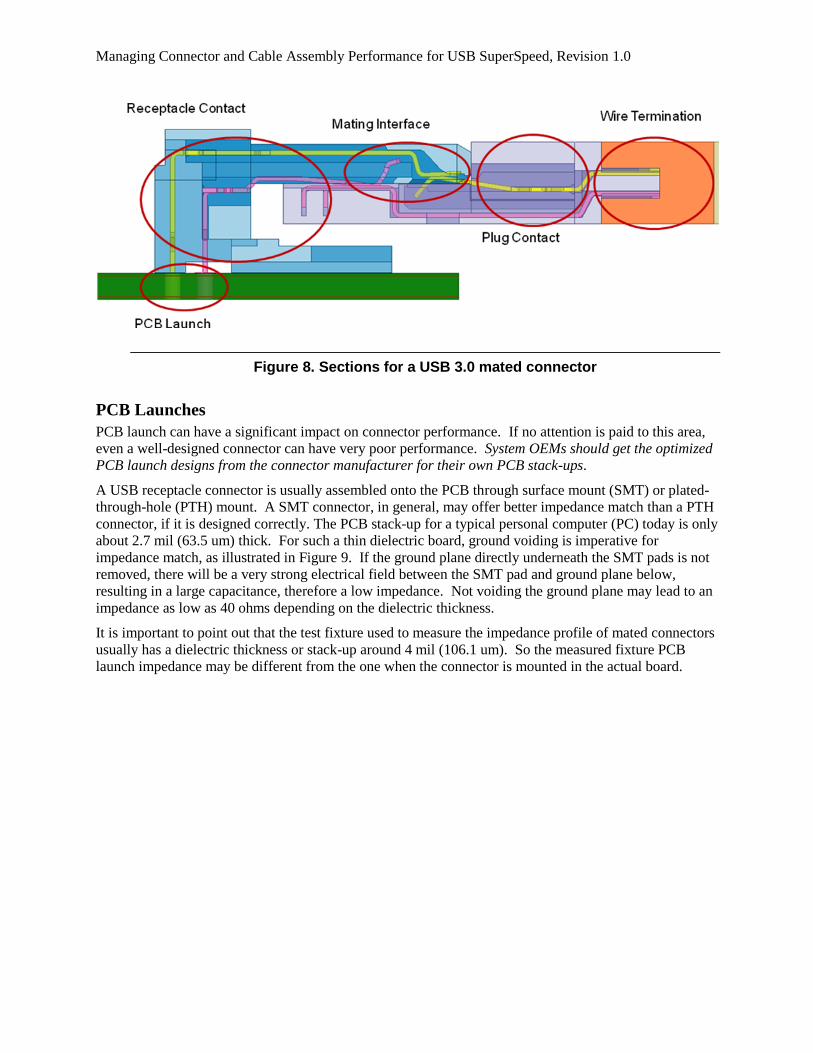
Managing Connector and Cable Assembly Performance for USB SuperSpeed, Revision 1.0
Figure 8. Sections for a USB 3.0 mated connector
PCB Launches
PCB launch can have a significant impact on connector performance. If no attention is paid to this area,
even a well-designed connector can have very poor performance. System OEMs should get the optimized
PCB launch designs from the connector manufacturer for their own PCB stack-ups.
A USB receptacle connector is usually assembled onto the PCB through surface mount (SMT) or plated-
through-hole (PTH) mount. A SMT connector, in general, may offer better impedance match than a PTH
connector, if it is designed correctly. The PCB stack-up for a typical personal computer (PC) today is only
about 2.7 mil (63.5 um) thick. For such a thin dielectric board, ground voiding is imperative for
impedance match, as illustrated in Figure 9. If the ground plane directly underneath the SMT pads is not
removed, there will be a very strong electrical field between the SMT pad and ground plane below,
resulting in a large capacitance, therefore a low impedance. Not voiding the ground plane may lead to an
impedance as low as 40 ohms depending on the dielectric thickness.
It is important to point out that the test fixture used to measure the impedance profile of mated connectors
usually has a dielectric thickness or stack-up around 4 mil (106.1 um). So the measured fixture PCB
launch impedance may be different from the one when the connector is mounted in the actual board.

Managing Connector and Cable Assembly Performance for USB SuperSpeed, Revision 1.0
Figure 9. Ground plane voiding for SMT connector
Figure 10 illustrates the PCB launch area of a USB 3.0 Standard-A receptacle connector. There are many
parameters that can impact the impedance in the PCB launch area; they include the PCB thickness, hole
size, pad size, anti-pad size, and the signal entry/exit layer.
Figure 10. PCB launch area of a USB 3.0 receptacle connector

Managing Connector and Cable Assembly Performance for USB SuperSpeed, Revision 1.0
The (finished) hole size of the recommended footprint defined in the USB 3.0 specification is 0.7 mm. A
smaller hole size may be used to improve impedance match. The smallest pad size that meets the
manufacturability requirement should be used; a large pad will make the PTH more capacitive. The anti-
pad is a ground void to prevent the shorting between the signal and ground. It is also used as a way to
reduce the capacitance for impedance match. We may have one anti-pad for each individual contact pin
(see the left picture of Figure 10), but the differential oval-shaped anti-pad is recommended for USB 3.0
receptacle (see the right picture of Figure 10) – a relatively large anti-pad is usually needed for impedance
match.
The PCB thickness is an important parameter. If the signal enters the connector from the top of the PCB
(top entry), then the PTH over the whole PCB thickness serves as the stub and there could be more
impedance mismatch. On the other hand, if the signal enters the connector from the PCB bottom, the stub
length will be zero and a better impedance match can generally be achieved. However, bottom entry is
not always better than top entry. It all depends on the PCB thickness and PTH hole and pad stack-up. It
is generally desirable to optimize the pad stack-up such that bottom and top entries have the same or
similar performance. A typical PCB thickness for desktop is about 0.062” (1.58 mm). For thicker PCB’s,
say >= 0.093”, it may be difficult to optimize the PCB launch performance to meet the USB 3.0
specification. In such a case, the SMT connector should be used. It is recommended that the
electromagnetic fieldsolver such as HFSS be used to optimize the PCB launch for specific stack-ups.
Besides providing the connector overall dimensions and footprint, the connector customer drawing should
also offer recommended pad stack-up, which include hole, pad and anti-pad sizes and shape, for
commonly used PCB stack-ups. System OEMs should ask for this.
Another commonly used technique for impedance match is called inductance compensation. For
example, we may create high inductance area with thin and small contact leads just above the PCB (see
Figure 10). The high inductance there will offset the capacitance from the PTH, resulting in better match.
Receptacle Contact
The receptacle contact region is between the PCB launch and mating interface, as illustrated in Figure 11.
This is an area that can be quite long, particularly for the double-, even quad- stacked connectors.
Figure 11. Illustration of the Receptacle Contact region

Managing Connector and Cable Assembly Performance for USB SuperSpeed, Revision 1.0
One almost has to treat this region as a transmission line for impedance match. Obviously, it is NOT
exactly a uniform transmission line. There are portions of the contacts in this region that are exposed to
air, or embedded in plastic housing, or mix of both, or with housing retention features. The main
parameters that impact the impedance are the contact width and dielectric material near the contacts. An
electromagnetic fieldsolver can be used to tune this region in order to have a characteristic impedance
about 90 ohms as uniform as possible.
To manage crosstalk, the spacing between the Tx and Rx differential pairs should maximized as much as
possible, which may be a trade-off with impedance match. Extra caution is needed to manage the
crosstalk between the SuperSpeed (USB 3.0) and HighSpeed (USB 2.0) contacts. The maximum
separation that is allowed by the geometry should be used, as illustrated in Figure 12. An offset between
the SuperSpeed and HighSpeed contacts such that the contact surfaces do not directly face each other)
will also reduce the crosstalk.
Figure 12. Maximizing spacing between SuperSpeed and HighSpeed contacts
Mating Interface
The mating interface is where the contacts on the receptacle mate with the contact on the plug. This is the
area we usually observe low impedance due to the stubs needed for mechanical reasons, as circled in
Figure 13. Minimizing the stub lengths while practically allowed and using a fieldsolver to tune and
check.
Figure 13. Stubs in the mating interface region

Managing Connector and Cable Assembly Performance for USB SuperSpeed, Revision 1.0
Plug Contact
The plug contact needs to be handled the same way as the receptacle contact. The contact portion that is
exposed in air and the one embedded in the plastic housing should be properly sized for impedance
match. Figure 14 shows an example of the plug contact in a Standard-B plug. The narrow and long
contact will result in a high impedance, exceeding the spec limit of 105 ohms.
Figure 14. Example of plug contact for the Standard-B cable plug
Wire Termination
Shown in Figure 15 is the comparison of near-end crosstalk for the USB 3.0 connectors from various
vendors. Given the fact that the Micro-B is very small and the contact designs from different vendors are
more or less the same, where does the difference in crosstalk come from?
Figure 15. Comparison of Micro-B connector crosstalk
The trick is the wire management in the wire termination area. Figure 16 shows the tear-down of two
USB 3.0 cable assemblies. The picture on the left side is a poorly managed wire termination area. The
excessively long strip where the shielding foil is removed can cause a large impedance mismatch and
crosstalk. The picture on the right side shows a well managed wire termination with a strip length around
2 mm. It is recommended the strip length be kept <=2.5 mm and drain wires be managed to be in close
proximity of the GND soldering pad.
0
0.5
1
1.5
2
2.5
3
3.5
4
4.5
Vendor1 Vendor2 Vendor3 Vendor4 Vendor5 Vendor6 Vendor7 Vendor8
Vendors
uB
NE
XT
, %

Managing Connector and Cable Assembly Performance for USB SuperSpeed, Revision 1.0
Figure 16. Managing wires in the wire termination area is important
Raw Cable
The USB 3.0 specification has an informative impedance requirement for SuperSpeed raw cable: 90 ohms
+/- 7 ohms. The raw cable is usually well behaved. Its main impact is on insertion loss due to the
conductor and dielectric losses. The typical wire gauge used for USB 3.0 may be from AWG 34 to AWG
26. For shorter cable, say less than 1 meter, smaller wire gauges (AWG 32 and AWG 34) should be
considered for ease of use. For long cable, say 3 meter long, AWG 26 will be needed to meet the -7.5 dB
insertion requirement.
Managing EMI and RFI
Systems that include USB 3.0 connectors and cable assemblies must meet the relevant EMI
(Electromagnetic Interference) and RFI (Radio Frequency Interference) requirements. Because of the
complex nature of EMI and RFI, it is difficult to specify a component level EMI and RFI requirements for
the connectors and cable assemblies. However, the quality of the connector and cable assembly shielding
does matter. Figure 17 shows the comparison of noise from two different USB 3.0 Standard-A
connectors; the one with improved shielding definitely radiates less [3].
To minimize the EMI and RFI risk, the connector and cable assembly designers, as well as system
implementers must pay attention to receptacle and cable plug shielding design to ensure a low impedance
grounding path. The following are guidelines for EMI and RFI management:

Managing Connector and Cable Assembly Performance for USB SuperSpeed, Revision 1.0
Figure 17. Improving connector shielding will reduce radiation
1. The USB 3.0 connector added two SuperSpeed differential pairs to the existing USB 2.0
connector form factor. Due to the geometrical constraint, there are only five contacts added: two
differential pairs separated by a single ground pin. By definition, this is not a symmetrical design
since one conductor in a differential pair is next to the ground pin while the other one isn’t.
Efforts should be made in design to avoid any additional asymmetry, which will manifesto itself
in terms the differential to common mode conversion and potentially EMI/RFI problems.
2. The quality of raw cables should be ensured. The intra-pair skew or the differential to common
mode conversion of the SuperSpeed pairs has a significant impact on cable EMI and RFI
performance and should be controlled within the limits of the USB 3.0 specification.
3. The cable external braid should be terminated to the cable plug metal shell as close to 360˚ as
possible. Without appropriate shielding termination, even a perfect cable with zero intra-pair
skew may not be able to meet EMI/RFI requirements.
4. If not done properly, the wire termination contributes to the differential-to-common-mode
conversion. The strip length or breakout distance for the wire termination should be kept as small
as possible for both EMI/RFI and signal integrity; as stated previously, the strip length should
not exceeding 2.5 mm. If possible, symmetry should be maintained for the two lines within a
differential pair.
5. The mating interface between the receptacle and cable plug shells should have a sufficient
number of grounding fingers, or springs to provide a continuous return path from the cable plug
to system ground. Friction locks should not compromise ground return connections.
6. The receptacle connector shell should have sufficient grounding legs to connect to the system
ground. It is recommended to have four grounding legs. Two grounding legs may not be enough
and is not recommended. Most receptacle connectors in use do have four grounding legs.
7. The receptacle connectors should be designed with a back-shield as part of the receptacle
connector metal shell. The back-shield should be designed with a short return path to the system
ground plane. Figure 18 shows an example USB 3.0 receptacle connector with back-shield and
four grounding legs or tabs for ground connection.

Managing Connector and Cable Assembly Performance for USB SuperSpeed, Revision 1.0
Figure 18. Example of a nearly fully shielded receptacle
8. The receptacle connectors should be connected to metal chassis or enclosures through grounding
fingers, screws, or any other way to mitigate EMI and RFI. Without such a connection, the EMI
and RFI performance will be compromised. This is the responsibility of system OEMs.
Mechanical Considerations
The USB 3.0 connectors are extension of the USB 2.0 connectors, and their mechanical considerations
should be similar. But the USB 3.0 connectors certainly need more careful design and manufacturing due
to the increased complexity over the USB 2.0 connectors.
Figure 19. SuperSpeed contact height
Managing Connector and Cable Assembly Performance for USB SuperSpeed, Revision 1.0
One aspect that recently caught the attention is the SuperSpeed contact height in the Standard-A cable
plug, as shown in Figure 19. To prevent shorting during insertion, the SuperSpeed contact blade surface
on the Standard-A receptacle is recessed by 0.28 mm nominal. Obviously, the SuperSpeed contact spring
on the cable plug must be high enough in order to make contact with the contact blade and to have a
sufficient normal force. However, it was found that this was not the case for some USB 3.0 cable
assemblies available in the market. To emphasis the importance of the contact height, there is a recent
ECN for the USB 3.0 specification, which explicitly requires a minimum contact height of 0.5 mm, as
shown in Figure 19.
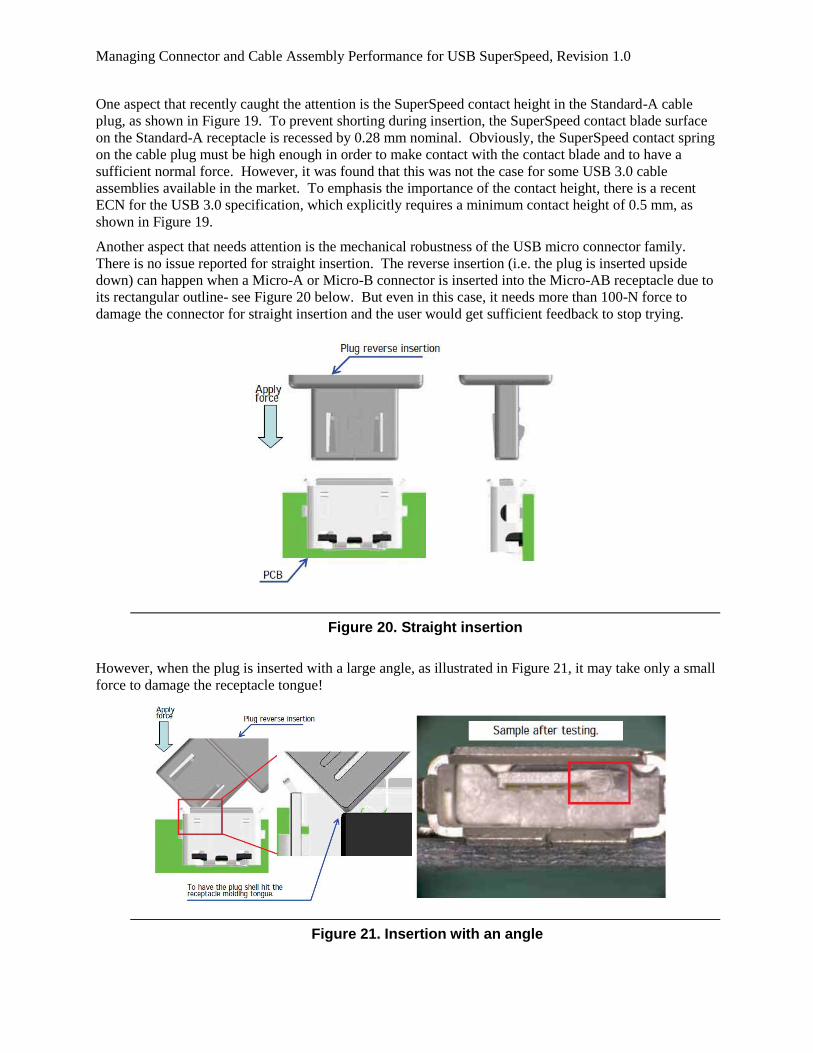
Another aspect that needs attention is the mechanical robustness of the USB micro connector family.
There is no issue reported for straight insertion. The reverse insertion (i.e. the plug is inserted upside
down) can happen when a Micro-A or Micro-B connector is inserted into the Micro-AB receptacle due to
its rectangular outline- see Figure 20 below. But even in this case, it needs more than 100-N force to
damage the connector for straight insertion and the user would get sufficient feedback to stop trying.
Figure 20. Straight insertion
However, when the plug is inserted with a large angle, as illustrated in Figure 21, it may take only a small
force to damage the receptacle tongue!
Figure 21. Insertion with an angle

Managing Connector and Cable Assembly Performance for USB SuperSpeed, Revision 1.0
Obviously, the insertion with such a large angle won’t happen often in normal usage. But OEMs that use
the USB Micro connectors should be aware of this. There may be options to improve the micro connector
tongue strength such as using a metal reinforced insert.
It should be pointed out that the USB Micro connectors are defined for handheld devices, not for PCs.
Extending their usage in PCs requires caution.
Conclusion
In this whitepaper, we have discussed the signal integrity impairments caused by the connectors and cable
assemblies. In particular, we have provided in-depth guidelines to manage the connector and cable
assembly signal integrity impairments for USB SuperSpeed, as well as the guidelines for EMI and RFI
management. High performance connectors and cable assemblies can be achieved following those
guidelines. A few mechanical considerations are also presented.
Related Documents
1. Universal Serial Bus 3.0 Connectors and Cable Assemblies Compliance Document, Revision 1.0.
USB-IF.
2. A Method for Evaluating Channels, Charles Moore and Adam Healey,100 Gb/s Backplane and
Copper Study Group, Singapore, March 2011.
3. USB 3.0 Radio Frequency Interference Impact on 2.4 GHz Wireless Devices, Intel whitepaper,
April, 2012.