MALLA REDDY COLLEGE OF ENGINEERING & …mrcet.com/downloads/digital_notes/HS/3 Engineering Physics...
77
MALLA REDDY COLLEGE OF ENGINEERING & TECHNOLOGY (An Autonomous Institution – UGC, Govt.of India) Recognizes under 2(f) and 12(B) of UGC ACT 1956 (Affiliated to JNTUH, Hyderabad, Approved by AICTE –Accredited by NBA & NAAC-“A” Grade-ISO 9001:2015 Certified) ENGINEERING PHYSICS - II B.Tech – I Year – II Semester DEPARTMENT OF HUMANITIES AND SCIENCES
-
Upload
nguyenhanh -
Category
Documents
-
view
215 -
download
2
Transcript of MALLA REDDY COLLEGE OF ENGINEERING & …mrcet.com/downloads/digital_notes/HS/3 Engineering Physics...

MALLA REDDY COLLEGE OF
ENGINEERING & TECHNOLOGY (An Autonomous Institution – UGC, Govt.of India)
Recognizes under 2(f) and 12(B) of UGC ACT 1956 (Affiliated to JNTUH, Hyderabad, Approved by AICTE –Accredited by NBA & NAAC-“A” Grade-ISO 9001:2015 Certified)
ENGINEERING PHYSICS - II
B.Tech – I Year – II Semester
DEPARTMENT OF HUMANITIES AND SCIENCES
CONTENTS
UNIT NAME OF THE UNIT
1 BONDING IN SOLIDS & CRYSTALLOGRAPHY
2 X RAY DIFFRACTION &DEFECTS IN CRYSTAL
3 DIELECTRICS
4 MAGNETIC PROPERTIES & SUPERCONDUCTIVITY
5 NANO TECHNOLOGY

MALLA REDDY COLLEGE OF ENGINEERING & TECHNOLOGY
B.TECH –I YEAR – II SEM L T/P/D C
2 1/-/- 2
(R17A0012) ENGINEERING PHYSICS-II
OBJECTIVES:
To understand the basics of bonding in solids, crystal structures and characterization
techniques.
To make the students aware of X-ray diffraction and different techniques of it.
To understand the behavior of dielectric materials, magnetic materials and nano materials.
UNIT-I
BONDING IN SOLIDS:
Types of bonds - Primary, Secondary, Forces between atoms, Expression for cohesive energy
between two atoms.
CRYSTALLOGRAPHY:
Space lattice, Basis, Unit cell, lattice parameters, Crystal systems, Bravais lattices, Atomic
number, coordination number, packing factor of SC,BCC,FCC crystals, Crystal planes and
directions - Miller indices. Expression for inter planar distance in cubic crystal, Structure of
NaCl and Diamond.
UNIT- II
X-RAY DIFFRACTION:
Bragg's law, Experimental techniques -Laue’s method, powder method, Applications of x-ray
diffraction.
DEFECTS IN CRYSTALS:
Classification of crystal defects, Point defects-Vacancies & Interstitials, Concentrations of
Schottky and Frenkel defects, Line defects- edge dislocation and screw dislocation, Burger’s vector.
UNIT-III
DIELECTRIC PROPERTIES:
Electric dipole, Dipole moment, Polarization vector (P), Displacement vector (D), Dielectric
constant (K), Electric susceptibility χ , Types of polarizations-Expression for Electronic and
Ionic polarization, Internal fields in dielectrics, Classius Mosotti relation, Piezo electricity and
Ferro electricity, Applications of dielectric materials.

UNIT-IV
MAGNETIC PROPERTIES:
Magnetic permeability, Field intensity, Magnetic field induction, Magnetization, Magnetic
susceptibility, Origin of Magnetic moment - Bhor magneton, Classification of magnetic
materials-Dia, Para and Ferro, Ferri and Anti ferro magnetic materials, Explanation of
Hysteresis loop on the basis of domain theory of ferromagnetism. Soft and hard magnetic
materials.
SUPER CONDUCTIVITY:
Super conductivity, Properties of super conductors, Meissner effect, Types –I Type-II super
conductors, Applications of super conductors.
UNIT-V
NANO SCIENCE & NANO TECHNOLOGY:
Nano scale, Types of Nano materials, Surface to volume ratio and Quantum confinement,
Bottom up Fabrication- Sol gel ,Top down Fabrication- Physical Vapour Deposition,
Characterisation of Nano particles –TEM and SEM, Applications of Nano materials.
TEXT BOOKS:
1. Engineering Physics - S Mani Naidu- Pearson Publishers.
2. A Text Book of Engineering Phyiscs- P.G. Kshirsagar, Avadhanulu – S.Chand
REFERENCES:
1. Solid State Physics, Kittel- Wiley International.
2. Solid State Physics – AJ DekKer-Macmillan Publishers.
3. Engineering Physics, P.K. Palaniswamy, Scitech Publishers
OUTCOMES:
The students would be able to learn the fundamental concepts on behavior of crystalline
solids.
The student will be able to think about the applications of dielectric, magnetic and nano
materials.
Finally Engineering physics course helps the student to develop problem solving
skills and analytical skills.

B.Tech I Year II Semester ENGINEERING PHYSICS II
DEPARTMENT OF HUMANITIES & SCIENCES ©MRCET (EAMCET CODE: MLRD) 1
Unit I Bonding in Solids & Crystallography
Introduction:
Bonding in any solids is the relation between the atoms in which it holds them
together. The force which keeps these atoms together in a solid is called inter atomic force
and is of two types- attractive force and repulsive force. Based on the strength of the bond,
bonding in solids is classified in two categories- (i) primary bonding & (ii) secondary
bonding.
Classification of chemical bonds:
Depending upon strength and directionality, bonds are divided into two type.
They are
I. Primary bonds.
II. Secondary bonds.
I. Primary bond or Interatomic bonds: The primary bonds are interatomic bonds. In this
bonding interaction occurs only through the electrons in the outermost orbit, i.e., valence
electrons. Primary bonds have bond energies in the range of 0.1-10 eV/bond. Primary
bonds are stronger and more stable than secondary bonds. The primary bonds are further
classified into three types namely
A. Ionic Or Electrostatic Or Electrovalent Bonds:
The bond formed between the two atoms by the transfer of electron is called Ionic
Bond. These bonds are formed between a metal and non metal.
Ex: NaCl , MgO, CaF2 ,.....etc.
Formation of NaCl:
The electronic configuration of the sodium atom is , , .It has one electron
more than neon. If it loses one electron from it’s outer most orbit it acquires a stable octent
configuration (Neon).
The electronic configuration of the chlorine atom is , , .It has one
electrons less compared to neon. If it gain one electrons acquires a stable octent
configuration (Argon).
When atoms of sodium and chlorine approach each other an
electron is transferred from Na to Cl atom. Both attain the octent electronic configuration
of the nearest Inert gases neon and argon respectively. Sodium atom becomes Na+
and
chlorine atom becomes Cl −.
Na +: Cl: → Na+Cl−
These two oppositely charged ions attract each other due to opposition charges and form
NaCl.
Na+ + Cl− → NaCl

B.Tech I Year II Semester ENGINEERING PHYSICS II
DEPARTMENT OF HUMANITIES & SCIENCES ©MRCET (EAMCET CODE: MLRD) 2
Properties of ionic substances:
Ionic substances are rigid; possess geometrical shape, hard and soluble in water.
It is easy to describe and visualize.
Ionic compounds exhibit high melting points.
Ionic compounds are soluble in polar solvents and insoluble in non polar solvents like
benzene, CCl , and other organic solvents.
Ionic compound conducts electricity both in matter state and also in aqueous
solutions.
Ionic bond is non directional bond. i.e., the magnitude of the bond is equal in all
directions around an ion.
B. Covalent or Electron-pair Bond: The bond formed between two atoms by the mutual
sharing of electron is called Covalent Bond. These bonds are formed between non-metals.
Covalent bond is further classified into two types
1. Non - Polar covalent bond.
2. Polar Covalent bond.
Non- Polar covalent bond: When two identical atoms combine they equally share the
bonding electron. Therefore each molecule has no charge separation and are called non
polar molecules. The bond formed between these atoms is called Non –Polar covalent
bond.
Ex: Cl2, O2 , N2.... etc.
Formation of Cl2: Atomic number of chlorine is 17. It’s electronic configuration is s s p s p . Each chlorine atom need one more electron to attain stability (Ar
electronic configuration). Each atom contributes one electron to form one pair of electron.
Both atoms share electron pair equally and forms one covalent bond. After bond formation
both the atoms gain the electronic configuration of Argon atom and the molecule becomes
stable. Molecules whose atoms are joined by covalent bonds are called covalent molecules.
The number of electron pairs shared in forming molecules is called covalence of the atom.
This shared pair is called the bonding pair of electrons. One pair of bonding electrons makes
one covalent bond. Thus a single bond forms between the two atoms in the chlorine
molecule. Cl + Cl → Cl Cl or Cl

B.Tech I Year II Semester ENGINEERING PHYSICS II
DEPARTMENT OF HUMANITIES & SCIENCES ©MRCET (EAMCET CODE: MLRD) 3
Polar Covalent Bond: When two unlike atoms combine one of them may attract the
bonding electrons more to itself than the other, resulting in unequal distribution of the
electron pair between them. Such a bond is called Polar Covalent bond.
Ex; HCl, H2O...
Formation of HCl: The electronic configuration of hydrogen and chlorine are s and s s p s p respectively. Each atom contributes one electron to form one pair of
electron. Both atoms share electron pair unequally and forms one covalent bond. Chlorine
atom attracts bonding electrons more than hydrogen atom and becomes partially negative
charged ( −) so it is considered as more electro negative than hydrogen atom. Due to this
hydrogen atoms acquires partial positive charge ( +). Such molecules possessing partial
positive and partial negative charges are called polar molecules. The establishment of partial
positive and partial negative centres in a bond is known as polarisation. Bond formed in this
way is called polar bond H + Cl → H Cl or Hδ+ − Clδ−
Properties of covalent compounds:
1. Covalent solids are hard, brittle and possess crystalline nature.
2. Covalent bond can be either very strong or very weak depending upon the atoms
involved in the bond.
3. Melting and boiling points of covalent compounds are lower than ionic compounds.
4. Covalent compounds are soluble in non polar solvents and insoluble in polar
solvents.
5. Covalent compounds are poor conductors of heat and electricity.
6. Covalent bond is not only rigid but is directional and has definite geometry about
them.
C. Metallic bond: The force that binds a metal atom to a number of electrons within its
sphere of influence is called Metallic bond.
Ex: Na, Au, Cu, Ag.....
It is existing both in metals and their
alloys. in metals, the metal atom lose their
outer electron to form metal cations. The
electrons from all the metal atoms form an
electron sea or cloud which can flow
throughout the space occupied by the atoms.
Those electrons are often described as
delocalised electrons. Metallic bonding is
different from both ionic and covalent
bonding. The metal cations and electrons are oppositely charged, and hence, they are
attracted by each other. The electrostatic forces are called Metallic Bonds.
The classical theory fails to explain the metallic character of solids
based on the number of valence electrons. Elements(Na, K etc.) having only one electron
in the outer most orbit are metallic in nature while elements(Mg, Al etc.) having 2 or 3
electrons in the outer most orbits are just metallic and the elements (tin and lead) having
4 electron in their outer most orbit are less metallic in nature. When the valence electrons
B.Tech I Year II Semester ENGINEERING PHYSICS II
DEPARTMENT OF HUMANITIES & SCIENCES ©MRCET (EAMCET CODE: MLRD) 4
becomes 6 or 7 these elements lose their metallic character. According to the quantum
mechanical concept, the metallic bond is regarded as an unsaturated covalent bond.
Properties of metallic solids:
1. Metallic bonds are relatively weak.
2. Metallic bond holds the atoms together in metals.
3. Metallic solids are malleable and ductile.
4. Metallic bond is non directional.
5. Metallic solids are not soluble in polar and nonpolar solvents.
6. Metals are opaque light.
7. They possess high electrical and thermal conductivity.
8. They have high number of electrons.
9.
II.Secondary bond or Intermolecular bonds: Secondary bonds have energies in the range
of 0.01 - 0.5 eV/bond. The secondary bonds are further classified into two types. They are
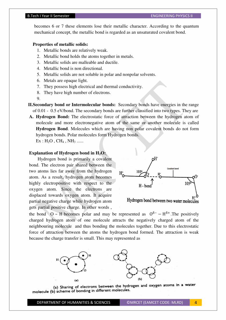
A. Hydrogen Bond: The electrostatic force of attraction between the hydrogen atom of
molecule and more electronegative atom of the same or another molecule is called
Hydrogen Bond. Molecules which are having non polar covalent bonds do not form
hydrogen bonds. Polar molecules form Hydrogen bonds.
Ex : H2O , CH4 , NH3 ......
Explanation of Hydrogen bond in H2O:
Hydrogen bond is primarily a covalent
bond. The electron pair shared between the
two atoms lies far away from the hydrogen
atom. As a result, hydrogen atom becomes
highly electropositive with respect to the
oxygen atom. Since the electrons are
displaced towards oxygen atom. It acquire
partial negative charge while hydrogen atom
gets partial positive charge. In other words ,
the bond O – H becomes polar and may be represented as Oδ− − Hδ+ .The positively
charged hydrogen atom of one molecule attracts the negatively charged atom of the
neighbouring molecule and thus bonding the molecules together. Due to this electrostatic
force of attraction between the atoms the hydrogen bond formed. The attraction is weak
because the charge transfer is small. This may represented as

B.Tech I Year II Semester ENGINEERING PHYSICS II
DEPARTMENT OF HUMANITIES & SCIENCES ©MRCET (EAMCET CODE: MLRD) 5
The hydrogen atom act as a bridge between two atoms holding one atom by covalent
bond and the other atom by a hydrogen bond. The hydrogen bond is represented by dotted
(..........) line and the covalent bond is represented by solid line (− ). Hence, hydrogen atom
also known as Hydrogen bridge. A typical covalent bond is only 20 times stronger than an
intermolecular hydrogen bond. These bonds can occur between molecules or within different
parts of single molecule. The hydrogen bond lies in between a covalent bond and an
electrostatic intermolecular attraction.
Properties of hydrogen solids:
1. Hydrogen bonded solids do not have any valence electrons and hence, they are solid
insulators.
2. Hydrogen bonds are weaker than primary bonds.
3. Hydrogen bonded solids are soluble both in polar and non polar solvents.
4. They are transparent to light.
5. They have low melting points.
6. Hydrogen bonds are directional.
7.
B. Van der walls bond or Dispersion bond:
The bonds between the molecules that allow sliding and rupture to occur are
called van der Waal forces or bonds.
Ex: Graphite, Inert gas solids like solid Argon, Organic symmetric molecule solids like
solid Methane. etc ...
Explanation: Consider two atoms of an inert gas having completed electronic shells. When
the atoms are at neutral, the positive and negative charge centres are exactly at the same
location. When the two atoms are brought together,a displacement of positive and negative
charge centres takes place relatively. Then, the positive and negative charges are separated.
As a result it creates an electric dipole. This dipole induces another dipole in neighbouring
atoms and force of attraction results. This force of attraction are usually called vander waals
forces. This interaction is very much weaker than the covalent interaction. These forces are
responsible for condensation of inert elements and gases like hydrogen, nitrogen, methane
etc. at very low temperatures.

B.Tech I Year II Semester ENGINEERING PHYSICS II
DEPARTMENT OF HUMANITIES & SCIENCES ©MRCET (EAMCET CODE: MLRD) 6
Properties of solids with vander wall bonding :
1. Van der waals bonds are non directional.
2. Van der waals bonding is weaker than the hydrogen bonding.
3. Van der waal bonded solids have low melting and boiling points.
4. They are usually transparent to light.
5. They are soluble in both polar and non polar liquids.
FORCES BETWEEN ATOMS:
When atoms are at infinite separation, then there is no interaction between them. As
the atoms come close to each other to form solids, there exist two types of forces between the
atoms 1.Attractive force 2. Repulsive force.
ATTRACTIVE FORCE: The forces that bring atoms together are called forces of
attraction. This force keep the atoms together and prevent the atoms moving away from each
other These attractive forces are inversely proportional to some power of distance between
particles or ions. The potential energy due to this force is negative because the atoms do work
of attraction. Attractive force F ∝ − r
F = − r
Where ‘a’ is proportionality constant , ‘r’ represents distance between
particles or ions. and ‘m’ is usually 2 as per
coulombs law.
REPULSIVE FORCE:
When the atoms approach closer than
inter nuclear distance (r0) the repulsive forces
between the two nuclei developed. The
repulsive forces are inversely proportional to
some power of distance between particles or
ions. The potential energy due to this force is
positive because external work must be done to bring two such atoms close together so that
they repel each other. Repulsive force Fr ∝ r
Fr = r
Where ‘b’ is proportionality constant, ‘r’ represents distance between particles
or ions. and ‘n’ is usually in between 7 to 10.
Resultant Force: The resultant force can be expressed as sum of both repulsive and
attractive forces.
F r = F + Fr
F r = − r + r n > m
When the system is at equilibrium, the distance between particles or
ions will be r = r then the magnitudes of the Fa and Fr is equal and opposite. So the
resultant force between atoms is zero.

B.Tech I Year II Semester ENGINEERING PHYSICS II
DEPARTMENT OF HUMANITIES & SCIENCES ©MRCET (EAMCET CODE: MLRD) 7
− r + r = r = r
r − =
= −
Cohesive energy or binding energy or dissosiation energy:
Def: The energy required to break the atoms of the solid into isolated atomic species.
Calculation of Cohesive energy:
The potential energy between the atoms can be
calculated by integrating the force of attraction.
= −∫
= −∫ − +
= ∫ −
= [ − +− + ] − [ − +− + ] +
= − [ − ] − + [ − ] − +c
= − + +c
Let = − , = − = − , = − and ‘c’ is constant of propagation.
Where A and B are force constants, M and N are positive integers. The value of ‘c’ can be
obtained by applying boundary conditions.
When , → ∞ , = , =
= − +
If the system is in equilibrium, then = and
tents to minimum value, 𝑖 . Therefore,
= 𝑖 = − +
Differentiating eq. w.r.t ‘r’
𝑼 = − − − − − For minima , first derivative =

B.Tech I Year II Semester ENGINEERING PHYSICS II
DEPARTMENT OF HUMANITIES & SCIENCES ©MRCET (EAMCET CODE: MLRD) 8
− − − − − = − − = − − =
= [ ] [ ] Substituting eq. in eq.
𝑖 = − + [ ] [ ]
𝑖 = − ( − )
𝑖 = ( − )
This is the expression for cohesive energy of a molecule containing two atoms in a molecule.
It is depending on distance between atoms, molecules and ions in a solid.
Crystal structures:
Crystallography:
Solid is characterized by structural rigidity and resistance to changes of shape or
volume. It is of two types: one in which the atoms are tightly bound to each other in a regular
geometric lattice (called crystalline solids) and another in which atoms are irregularly spaced
(called a non-crystalline or an amorphous solids). “Crystallography is a branch of science that
deals with the formation, properties and structure of crystals:
Crystalline Solids: 1. They have a regular periodic (three dimensional) arrangement of atoms, ions or
molecules.
2. They have long range order.
3. They have sharp melting point i.e., they melt at a particular temperature.
4. They are anisotropic, i.e., they have different (optical and electrical) properties in different
directions.
5. Examples: Metals, NaCl, diamond, etc.
Amorphous Solids:
1. They have an irregular three dimensional arrangement of atoms, ions or molecules.
2. They have short range order.
3. They do not have sharp melting point i.e., they melt over a range of temperature.

B.Tech I Year II Semester ENGINEERING PHYSICS II
DEPARTMENT OF HUMANITIES & SCIENCES ©MRCET (EAMCET CODE: MLRD) 9
4. They are isotropic, i.e., they have same properties in all directions.
5. Examples: Glasses, rubber, plastic, etc.
Fundamental definitions:
(a) Lattice Point: It is an imaginary point in space, which locates the position of atom (s) or ion (s) or
radicals or molecules.
(b) Space Lattice:
It is a three dimensional arrangement of lattice points in
space in which every lattice point has an identical environment.
(c) Translational Vector: Image of space lattice
The translation vector is the distance through which an atom must be moved
(translated) in order to be in the next unit cell. In the crystal
structure so formed, each lattice point has identical surroundings. It
means that the lattice points are connected by a translation operator
T, where T is defined as T= n1a+n2b+n3c, where n1, n2, and n3 are
integers and a, b, c are primitive or fundamental translation
vectors.
(d) Basis:
It represents a group of atoms or ions or radicals or molecules. Basis in combination
with space lattice forms a crystal structure.
(e) Unit Cell:
It is defined as the smallest geometric figure (or pattern) the
repetition of which, in three dimensions, gives the complete crystal
structure.
Primitive cell is a unit cell having only one lattice point. The atoms
lie only at the corners.
Non-primitive cell is a unit cell having more than one lattice point. Atoms may lie on
the faces or along the body diagonals apart from being present at the corners.

B.Tech I Year II Semester ENGINEERING PHYSICS II
DEPARTMENT OF HUMANITIES & SCIENCES ©MRCET (EAMCET CODE: MLRD) 10
(f) Lattice parameter:
The lattice constant, or lattice parameter, refers to the
physical dimension of unit cell in a crystal lattice. Lattices in three
dimensions generally have three lattice constants, referred to as a, b,
and c and three interfacial angles α, and .
(g) Bravais Lattice:
There are 14 distinguishable ways of arranging the lattice points in space, which
constitutes the seven crystal system.
In 3D there are 7 crystal systems as mentioned below:
Crystal
System
Unit Cell
Dimension
s
Bravais Lattice Examples
Cubic a=b=c
α= = =90o
NaCl,
ZnS, Cu
Tetragonal a=b≠c
α= = =90o
SnO2,
TiO2,
CaSO4
Orthorhombic a≠b≠c
α= = =90o
KNO3,
BaSO4
Monoclinic a≠b≠c
α = =90o≠
Na2SO4.10
H2O

B.Tech I Year II Semester ENGINEERING PHYSICS II
DEPARTMENT OF HUMANITIES & SCIENCES ©MRCET (EAMCET CODE: MLRD) 11
Triclinic a≠b≠c
α ≠ ≠
K2Cr2O7,
CuSO4.5H
2O
Trigonal/
Rhombohedra
l
a=b=c
α= = ≠90o
Calcite
(CaCO3),
Cinnabar
(HgS)
Hexagonal
a=b≠c
α= =90o;
=120o
Graphite,
ZnO, CdS
Definitions:
(a) Atomic Radius:
It is half of the distance between the centre of the two atoms.
(b) Coordination Number:
It is defined as the number of equidistant neighbouring atoms to a parent atom or
reference atom.
(c) Packing Factor:
It is defined as the ratio of the volume of atoms to the volume of unit cell.
Mathematically it is given by,
𝑖 = 𝑖
Packing Factor of Bravais Lattices
Simple Cubic Structure: It is a structure, in which eight atoms are present at the eight
corners, such that:
Coordination number = 6
Number of atom(s) per unit cell (n) = 8 × 1/8 = 1
Atomic radius = r & lattice constant = a

B.Tech I Year II Semester ENGINEERING PHYSICS II
DEPARTMENT OF HUMANITIES & SCIENCES ©MRCET (EAMCET CODE: MLRD) 12
Relation between a & r: From figure, a=2r
𝑖 = × 𝑖
Volume of atom of radius ‘r’= 𝜋
Volume of unit cell of side ‘a’= a3
Therefore, P.F. = × 𝜋𝑟 (where a=2r)
P.F. = × 𝜋𝑟
By solving the above equation, P.F. = 0.52.
Body Centered Cubic (BCC): It is a structure in which eight atoms are present at the eight
corners and one at the centre of the body (along the body diagonal), such that:
Coordination number = 8
Number of atom(s) per unit cell (n) = (8 × 1/8) + 1 = 2
Atomic radius = r & lattice constant = a
Relation between a & r:
From figure: AC2 = AB
2 + BC
2
AC
2 = a
2 + a
2 =› AC2
= 2a2
=› AC =√2 a
Also, AD2 = AC
2 + CD
2
AD
2 =2a
2 + a
2 =› AD2
= 3a2
=› AD =√3 a
From figure, AD = 4r= √3 a or, a=4r/√3 𝑖 = × 𝑖
Therefore, P.F. = × 𝜋𝑟 (where a=4r/√3)
P.F. = × 𝜋𝑟𝑟√
By solving the above equation, P.F. = 0.68.
Face Centered Cubic (FCC): It is a structure in which eight atoms are present at the eight
corners and six on the six faces of the cube (along the face diagonal), such that:
Coordination number = 12
Number of atom(s) per unit cell (n) = (8 × 1/8) + (6 × 1/ 2) = 4

B.Tech I Year II Semester ENGINEERING PHYSICS II
DEPARTMENT OF HUMANITIES & SCIENCES ©MRCET (EAMCET CODE: MLRD) 13
Atomic radius = r & lattice constant = a
Relation between a & r:
From figure: AD2 = AC
2 + CD
2
AD
2 =a
2 + a
2 =› AD2
= 2a2
=› AD =√2 a
Fom figure, AD = 4r= √2 a or, a=4r/√2 𝑖 = × 𝑖
Therefore, P.F. = × 𝜋𝑟 (where a=4r/√2)
P.F. = × 𝜋𝑟𝑟√
By solving the above equation, P.F. = 0.74.
Crystal directions and planes- Miller Index:
It is often necessary to specify certain directions and planes in crystals, as many material
properties and processes vary with direction in the crystal. Directions and planes are
described using three integers called Miller Index.
Crystal directions-Method:
1. Draw vector, and find the coordinates of the head (x2, y2, z2) and the tail (x1, y1, z1)
2. Subtract coordinates of tail from coordinates of head
3. Remove fractions by multiplying by smallest possible factor
4. Enclose the above whole number obtained in square brackets i.e., [h k l] called Miller
index.
Example: To obtain the direction of OP.
Consider the coordinates of O & P as (0, 0, 0) & (1, 1, 1)
respectively.
- Subtract the coordinates of P from the coordinates of O i.e.,
(1-0, 1-0, 1-0)
- Convert the fractions, if any so, into whole number by
multiplying the fractions by smallest possible factor
- Enclose the above whole number in square brackets i.e.,
[1 1 1] which represents the Miller index corresponding
to the direction OP.
The figure shows some of the crystal directions:
[1 0 0]; [1 1 0]; [1 0 1]; [0 1 2] & [2 2 1]

B.Tech I Year II Semester ENGINEERING PHYSICS II
DEPARTMENT OF HUMANITIES & SCIENCES ©MRCET (EAMCET CODE: MLRD) 14
Crystal Planes-Miller Index:
Miller index of a plane is the smallest value (or integer) obtained from the reciprocal
of the intercepts of the plane in the crystal. It is denoted by (h k l).
Method:
1. Obtain the intercept of the plane, let it be pa + qb + rc where p, q, r are value of the
intercepts
2. Take the reciprocal of p, q, r i.e., 1/p, 1/q, 1/r
3. Convert the above fractional values into whole numbers (by taking the LCM of the
denominator and multiplying each fractional value)
4. We obtain the Miller index (h k l)
Example: If intercept made by a plane is (2a, 3b, c) then find its Miller index.
Soln: Intercept value: 2, 3, 1
Reciprocal: 1/2, 1/3, 1/1
LCM of denominator: 6
Therefore, 6 × 1/2, 6 × 1/3, 6 × 1/1 i.e., 3, 2, 6
Miller Index, (h k l) = (3 2 6)
Features of Miller Indices:
1. The intercept of a plane parallel to any axis is infinity and thereby its corresponding
Miller index is zero.
2. When the intercept of a plane is negative, the corresponding Miller index is
represented by putting a bar on it.
3. All equally spaced parallel planes have same index number (h k l).
4. If a normal is drawn to a plane (h k l), the direction of the normal is [h k l].
Examples of crystal planes with Miller Index: (100); (110) and (111)

B.Tech I Year II Semester ENGINEERING PHYSICS II
DEPARTMENT OF HUMANITIES & SCIENCES ©MRCET (EAMCET CODE: MLRD) 15
Interplanar Spacing (or interatomic spacing) between successive (h k l) crystal planes:
For Cubic Crystal System:
Consider a cubic crystal system of sides ‘a’ unit, consisting of n successive parallel
planes represented by Miller index (h k l).
Assume a plane ABC, shown in figure-(a), at a distance of ON=d1 from the origin.
The angle made by the plane ABC with the respective X, Y and Z axes is given by α, , and .
From figure, OA=a/h; OB=a/k and OC=a/l
Cos α=d1/OA; Cos =d1/OB and Cos =d1/OC
From cosine law:
+ + = ∴ / + / + / =
= › ℎ + + =
=› solving further, = ℎ + +
= √ ℎ + + ……… .
To determine the interplanar spacing, consider another plane A΄B΄C΄ at a distance of OM=d2 from the origin and making same angles α, , and with the respective X, Y and Z
axes.
Therefore,
΄ = /ℎ; ΄ = / ΄ = /
= / ΄; = / ΄ = / ΄
From cosine law:
+ + =
Therefore, / ΄ + / ΄ + / ΄ =

B.Tech I Year II Semester ENGINEERING PHYSICS II
DEPARTMENT OF HUMANITIES & SCIENCES ©MRCET (EAMCET CODE: MLRD) 16
= › ℎ + + =
Solving further, = ℎ + +
== √ ℎ + + ………… .
From equations (1) and (2):
= – = › = √ ℎ + + ……………
Equation (3) shows the interplanar spacing between successive (h k l) planes which is equal
to the distance of first plane ABC from the origin.
For a tetragonal crystal system: a=b≠c and α= = =90o therefore, = ℎ + +
= [ ℎ + + ]
Similarly for Orthorhombic crystal system: a≠b≠c and α= = =90o
d = [ ha + kb + lc ]
Other Crystal Structure:
Diamond:
Diamond structure is formed by the interpenetration of one FCC sub-lattice into another
FCC lattice. The resultant structure formed consists of eight atoms at eight corners and six
atoms on the six faces, belonging to one FCC sub-lattice, and four atoms along the four body
diagonals, belonging to second FCC sub-lattice.

B.Tech I Year II Semester ENGINEERING PHYSICS II
DEPARTMENT OF HUMANITIES & SCIENCES ©MRCET (EAMCET CODE: MLRD) 17
The four atoms present along the body diagonals are arranged in the lattice in such a
manner that- two atoms is at a distance of a/4 and other two atoms at 3a/4.
From figure the four body diagonal atoms are:
Along AG and CE at a/4 from face ABCD and along BH and DF at 3a/4 from face ABCD.
The arrangement of four atoms along the body diagonals looks symmetric from all the faces.
Number of atoms per unit cell= (8 × 1/8) + (6 × 1/ 2) + 4= 8
Coordination Number= 4; Packing Factor= 0.34
Sodium Chloride (NaCl) Structure:
NaCl structure is formed by the
interpenetration of one FCC sub lattice into another
FCC lattice. It consists of Na and Chloride ions
occupying the alternate positions in the structure as
shown in figure. The various positions of:
Na ion: (1/2,0,0); (0,1/2,0); (0,0,1/2); (1/2,1/2,1/2);
etc.
Cl ion: (0,0,0); (1,0,0); (0,1,0); (0,0,1); (1,1,1); etc.
Number of atoms per unit cell: 8
Top face= (4 × 1/8) + (1 × 1/ 2) + 4 × 1/ 4= 2
Middle layer= (4 × 1/4) + +1 + (4 × 1/ 2) = 4
Bottom layer= (4 × 1/8) + (1 × 1/ 2) + 4 × 1/ 4= 2
Coordination Number= 6

B.Tech I Year II Semester ENGINEERING PHYSICS II
DEPARTMENT OF HUMANITIES & SCIENCES ©MRCET (EAMCET CODE: MLRD) 18
UNIT II X-RAY DIFFRACTION
X-RAY DIFFRACTION BY CRYSTAL PLANES:
X- ray diffraction is defined as bending of x-rays around the obstacle. x- rays are EM waves
like ordinary light, therefore they should exhibit interference and diffraction. The X-rays
produce diffraction when the size of opaque obstacle must be comparable to the wavelength.
If x-rays wavelength is less than the opaque obstacle, it can’t produce x-ray diffraction. To
obtain diffraction effects with x-rays the rulings in a diffraction grating must be spaced only a
few nano meters. But this is very complicated or practically this is not possible. To avoid this
problem Laue suggested a crystal because of the distance between atoms are very low and it
works as 3D grating. Hence it is known as crystal grating, whereas optical grating is a 2D
plane grating.
W.L. Bragg observed x - ray diffraction when X- rays are incident on the
crystal surface nearly at Bragg’s angles. Bragg’s angle or glancing angle means the angle
between incident ray and crystal plane at which diffraction occurs.
BRAGG’S LAW:
Statement: The X- rays reflected from different parallel planes of a crystal interfere
constructively when the path difference is integral multiple of the wavelength of X-rays.
Explanation:
Let us consider a crystal made up of a
equidistant parallel planes of atoms with
the inter planar spacing ‘d’. Let a narrow
beam of X - rays of ′ ’ be incident on
the planes with a glancing angle θ then a
part of the X- ray beam AB incident at B
in plane-1 is scattered along the
direction BC. Similarly a part of the X-
ray beam DE incident at E in plne-2 is
scattered along the direction EF and it is parallel to BC. Let the beams AB and DE make
angle θ with the planes. This angle θ is called as angle of diffraction or glancing angle.
The path lengths of ABC and DEF are not same .To find the path difference between
ABC and DEF, extend the rays AB to cut EF at Q and CB to cut DE at P. Path length of
the ray DEF greater than the path length of ABC by an amount (PE+EQ). ∴ The path difference between two rays reflected from adjacent planes δ = PE+EQ (1)
The rays BC and EF will be in phase only when,
δ = n (n = 0,1,2,3.......)
From the fig. ∆ PBE and ∆QBE are each equal to θ only. The length BE is equal to ‘d’.
From ∆ PBE, sinθ = PEE =
PE

B.Tech I Year II Semester ENGINEERING PHYSICS II
DEPARTMENT OF HUMANITIES & SCIENCES ©MRCET (EAMCET CODE: MLRD) 19
PE = d sinθ (2)
Similarly, ∆ QBE, EQ = d sinθ (3)
Sub (2) and (3) in eq. (1) ∴ path difference δ = PE+EQ. ∴ path difference δ = d sinθ + d sinθ
∴ path difference δ = 2d sinθ
Therefore, for the rays in phase, d sinθ = n
Since the maximum possible value for θ is 1. λ ≤
The wavelength λ should not be exceed twice the inter planar spacing for diffraction to occur.
Methods to determine crystal structure:
According to Bragg’s equation, for a given wavelength, diffraction can take place only when
‘θ’ and’d’ are matched. For this purpose either θ or d has to be allowed to vary continuously
so that Bragg’s condition is satisfied and diffraction takes place.
As an alternative, we make θ and d constant and use a continuous range of wavelengths. This
can be accomplished by three main X – ray diffraction methods by which the crystal
structures can be analyzed.
I. Laue method ∶ − For single crystal.
II. Powder method ∶ − Polycrystalline powder.
III.Rotating crystal method ∶ − For single crystals.
Laue method:

B.Tech I Year II Semester ENGINEERING PHYSICS II
DEPARTMENT OF HUMANITIES & SCIENCES ©MRCET (EAMCET CODE: MLRD) 20
In this method , white X – rays (X – radiation with continuous wavelength) over a wide range
of wavelengths preferably from 0.2 to 2 A° sent through pin holes made up of a lead sheets to
obtain fine sharp beams.
The sharp beam of x – rays are made to incident on the crystal which is kept
stationary on a crystal holder. Thickness of crystal are usually 0.5 mm and it’s length and
breadth are about mm × mm .The crystal act as a 3D diffraction grating. The rays after
passing through the crystal are diffracted and are recorded on the photographic film placed at
certain distance from the crystal. Developed photographic film consists of large number of
dots. Each dot is known as Laue spot and the entire spots are called as Laue diffraction
pattern. Each Laue spot represents a set of Miller indices of plane in the crystal. The
diffracted X – rays from a set of plane produce constructive interference, if they are in phase
and form an intense beam and this produce dark spot on photographic film. If the diffracted
rays are out of phase, destructive interference takes place so that photographic film is
unaffected.
There are two practical variants of Laue method
Transmission Laue method - In this the film is placed behind the
crystal to record beams which are transmitted through the crystal.
In this Laue patter look like either ellipse.
Back reflection Laue method – In this the film is placed between
the x – ray source and the crystal. The beams which are diffracted
in a backward direction are recorded. In this Laue pattern look
like hyperbola.
Advantages:
1. The shape of the unit cell can be established from the symmetry of the Laue pattern.
2. Practically this method is used to evaluate (h k l) values of various planes from different
Laue spots.
3. Laue technique is extensively used to study defects in solids under mechanical and
thermal treatments.
Disadvantages:
Cell parameters of a crystal cannot be determined using Laue method. For transmission Laue
method the crystal should be thin. This method is not very useful in the overall study of the
crystal structure.
Limitations:
Interpretation of Laue pattern is quite complex. Special methods such as stereographic
projections have to be adopted.
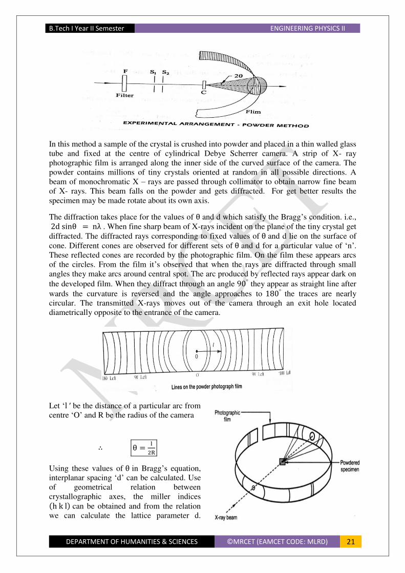
Powder method (Debye and Scherrer Method):
This method is a power full experimental technique which can be used for substances which
are not obtained easily in the form of single crystal of appreciable sizes. This method was
developed by Debye and Scherrer.
B.Tech I Year II Semester ENGINEERING PHYSICS II
DEPARTMENT OF HUMANITIES & SCIENCES ©MRCET (EAMCET CODE: MLRD) 21
In this method a sample of the crystal is crushed into powder and placed in a thin walled glass
tube and fixed at the centre of cylindrical Debye Scherrer camera. A strip of X- ray
photographic film is arranged along the inner side of the curved surface of the camera. The
powder contains millions of tiny crystals oriented at random in all possible directions. A
beam of monochromatic X – rays are passed through collimator to obtain narrow fine beam
of X- rays. This beam falls on the powder and gets diffracted. For get better results the
specimen may be made rotate about its own axis.
The diffraction takes place for the values of θ and d which satisfy the Bragg’s condition. i.e., d sinθ = n . When fine sharp beam of X-rays incident on the plane of the tiny crystal get
diffracted. The diffracted rays corresponding to fixed values of θ and d lie on the surface of
cone. Different cones are observed for different sets of θ and d for a particular value of ‘n’. These reflected cones are recorded by the photographic film. On the film these appears arcs
of the circles. From the film it’s observed that when the rays are diffracted through small
angles they make arcs around central spot. The arc produced by reflected rays appear dark on
the developed film. When they diffract through an angle ° they appear as straight line after
wards the curvature is reversed and the angle approaches to ° the traces are nearly
circular. The transmitted X-rays moves out of the camera through an exit hole located
diametrically opposite to the entrance of the camera.
Let ‘l ′ be the distance of a particular arc from
centre ‘O’ and R be the radius of the camera
∴ θ = R
Using these values of θ in Bragg’s equation,
interplanar spacing ‘d’ can be calculated. Use
of geometrical relation between
crystallographic axes, the miller indices h k l can be obtained and from the relation
we can calculate the lattice parameter d.

B.Tech I Year II Semester ENGINEERING PHYSICS II
DEPARTMENT OF HUMANITIES & SCIENCES ©MRCET (EAMCET CODE: MLRD) 22
d = a√h + k + l
Uses: The powder method is a standard technique used to study the structure of micro
crystals. This technique gives useful information regarding the size of the crystals, presence
of impurities, distortions, preferred orientation etc.
Applications:
X- ray diffraction are used
1. In analysis of solid and liquid samples.
2. In the study of nanometer composition.
3. In structural quality of pharmaceutical and organic compounds.
4. It is much useful to study crystal symmetry.
5. In determining the percentage of material in crystalline form versus amorphous.
6. In measuring residual stress in bulk metals and ceramics.

B.Tech I Year II Semester ENGINEERING PHYSICS II
DEPARTMENT OF HUMANITIES & SCIENCES ©MRCET (EAMCET CODE: MLRD) 23
CRYSTAL DEFFECTS
Introduction∶ The metals are made up of infinite number of atoms in space whose arrangement conforms to
a particular symmetry. The deviations from periodicity in the solid are called the defect in a
solid. Crystal imperfections refer to some irregularities in crystal structure in one or more
atomic distances. Sometimes, crystal defects are introduced intentionally into the lattice in a
controlled manner to achieve the required properties.
The solid materials are crystalline in structure. The crystals are divided into two groups, real
crystals or grown crystals and ideal crystals or sound crystals . If the arrangement of
atoms in a crystal is perfect, regular and continuous throughout the crystal, it is known as an ‘ ideal crystal ’. In practice, the ideal crystals rarely exist. The crystals in any material have
many defects, which may be due to various reasons. There will be irregularity or defects in
the arrangement of atoms within the crystal. These types of crystals are known as ’real
crystals’. The defects influence few properties of solid like colour of crystals, plasticity,
increased conductivity of pure semiconductors, melting, strength of crystals, luminescence,
diffusion of atoms through solids etc.
Reasons for crystal imperfections ∶ 1. Improper growth of crystals during crystallization.
2. Presence of impurities.
3. Application of local pressure on crystalline solid.
4. Effect of temperature.
Effect of defects on properties of solids ∶ 1. It lowers the tensile strength.
2. It increases brittleness.
3. It lowers mechanical strength (hardness, toughness, etc.)
4. Impurities of the crystal, lowers melting point of the crystal.
5. It changes refractive index.
6. Formation of holes/ vacancies increases thermal/ electrical conductivity.
Defects are produced by various methods ∶
1. By heating & rapid cooling
2. By applying external strength
3. By bombarding with high energy particles like neutrons or particles from cyclotron
B.Tech I Year II Semester ENGINEERING PHYSICS II
DEPARTMENT OF HUMANITIES & SCIENCES ©MRCET (EAMCET CODE: MLRD) 24
Classification of defects:
The defects are generally classified according to their dimensions are as follows :
Crystalline defects
I. 0 – Dimensional defects or Point defect.
1. Vacancies
2. Interstitial
3. Compositional defects
i. Substitutional impurity
ii. Interstitial impurity.
4. Electronic defects
II. 1 – Dimensional defects or Line defects or dislocations.
1. Edge dislocation
2. Screw dislocation
III. 2 – Dimensional defects or Surface defects.
1. Grain boundaries
2. Twin boundaries
3. Tilt boundaries
4. Stacking fault
IV. 3 – Dimensional defects or Volume defects.
1. Air bubbles
2. Internal cracks
3. Empty spaces
Zero – dimensional defects 𝐎𝐑 point defect:
Zero dimensional defects arise due to missing of an atom from the regular position, presence
of impurity atom or atom in the wrong place during crystallization. The presence of point
defect in a crystal increases its internal energy compared to that of perfect crystal. The effect
of such defect is local and produces distortion inside the crystal. These are small defects
which extends its influence in all directions but limited to one or two atomic diameters in the
crystal lattice. Hence, the mechanical strength at that point gets reduced. There are different
kinds of point imperfections.
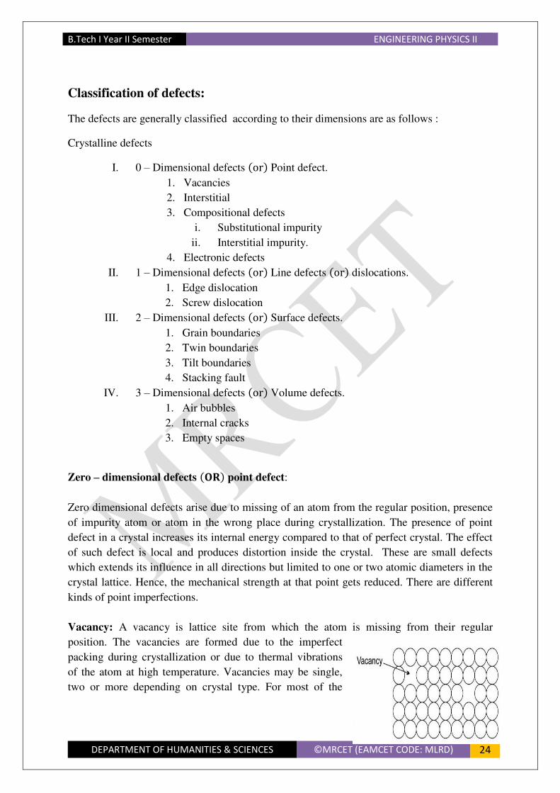
Vacancy: A vacancy is lattice site from which the atom is missing from their regular
position. The vacancies are formed due to the imperfect
packing during crystallization or due to thermal vibrations
of the atom at high temperature. Vacancies may be single,
two or more depending on crystal type. For most of the

B.Tech I Year II Semester ENGINEERING PHYSICS II
DEPARTMENT OF HUMANITIES & SCIENCES ©MRCET (EAMCET CODE: MLRD) 25
crystals, in order to create one vacancy thermal energy of 1.1 eV is required.
Interstitial defect:
This defect arises when an atom of same kind or different
kind occupies the void space (empty space between the
atoms) between the regular atomic sites. The
interstitial atom may be present in the crystals which have
low packing fraction. This atom causes some mechanical
strain on the surrounding atoms. The amount of the strain depends on the size of the
interstitial atom This atom is considerably smaller than the parent atoms otherwise it will
produce atomic distortion. Interstitials may be single interstitial, di-interstitials and tri-
interstitials.
Compositional defects:
Compositional defects arise due to presence of either unwanted impurities or purposely doped
impurities during the process of crystallization. These defects play an important role in
semiconductors which are specially prepared for diodes, transistors, etc. Impurity atoms are
present at the sites of regular parent atoms or in the interstitial spaces. These defects are two
types.
Substitutional impurities:
This defect arises when an impurity atom replaces or substitutes parent atom in the crystal
lattice. If the size of substitutional impurity is same as parent atom then the amount of strain
around will be less, otherwise it will be more.
Ex: In extrinsic semiconductors either third or fifth group atoms occupy the sites of silicon or
Germanium atoms.
Interstitial impurity: This defect arises when small sized foreign atom occupying an
interstice or void space in the parent crystal without disturbing any of the parent atoms from
their regular sites.
Ex: In steel, carbon atom (0.77r A° ), being smaller in size, occupies interstitial
position in Iron (2.250 r A° ).

B.Tech I Year II Semester ENGINEERING PHYSICS II
DEPARTMENT OF HUMANITIES & SCIENCES ©MRCET (EAMCET CODE: MLRD) 26
Point defects in ionic crystal:
In ionic crystal, point defects are of two types.
A. Stoichiometric defect.
B. Non – Stoichiometric defect.
Stoichiometric defect: The compounds in which the number of cation and anions are exactly
in the same ratio as represented by their chemical formula are called stoichiometric
compounds. The defects that do not disturb the ratio of cations and anions are called
stoichiometric defect.
Schottky defect:
The defect arises when equal number of cations and anions are missing from the lattice is
called schottky defect. This ion pair moves to the surface of the crystal, so that charge
neutrality is maintained in the vacancy region. Schottky defect decreases density of
crystalline substance. In this defect both anion and cation have similar sizes. This type of
defect occurs in ionic solids with high co-ordination number
Ex: Alkali halides (NaCl , CsCl, etc.)
Frenkel defect:
The defect arises when some of the ions (cations) of the lattice occupy an interstitial sites
leaving lattice sites vacant is known as Frenkel defect. Anoins do not get displaced like
cation, as the void space is just too smaller for their size. Here, charge neutrality is
maintained. Due to this defect there is no change in the density of the crystal. In this defect
anions are larger in size as compared to cations. This type of defect occurs in ionic solids
with comparatively low – co ordination number.

B.Tech I Year II Semester ENGINEERING PHYSICS II
DEPARTMENT OF HUMANITIES & SCIENCES ©MRCET (EAMCET CODE: MLRD) 27
Ex : CaF2, AgBr, AgI, etc.
Non – Stoichiometric defect (Electronic defect):
If as a result of imperfection, the ratio of number of cation to anion becomes different from
that indicated by the ideal chemical formula; the defects are called non – stoichiometric
defects. These defects arise either due to excess of metal atoms or non metal atom or
presence of impurities / foreign particle. By the influence of external electrical field, these
defects movie freely within the crystal. In semiconductors, temperature variation change
charge concentration, so variation of temperature [i.e., thermal energy] leads to electronic
defect. Non-stoichiometric Defects is mainly of two types –
Metal Excess Defect:
Metal excess defects are of two types:
(a) Metal excess defects due to anionic vacancies: A negative ion may be missing from its
lattice site, leaving a hole, which is occupied by an electron there by maintaining an electrical
balance. The trapped electrons are called F-centers or colour centers because they are
responsible for imparting colour to the crystal. Alkali halides like NaCl and KCl shows this
type of defect.
Ex: When crystals of NaCl are heated in an atmosphere
of sodium vapour, the sodium atoms are deposited on the
surface of the crystal. The Cl− ions diffuse to the surface
of the crystal and combine with Na atoms to give NaCl.
This happens by loss of electron by sodium atoms to form Na+ ions. The released electrons diffuse into the crystal
and occupy anionic sites. As a result the crystal now has
an excess of sodium. The anionic sites occupied by
unpaired electrons are called F-centres (from the German
word Farbenzenter for colour centre). They impart yellow
colour to the crystals of NaCl. The colour results by excitation of these electrons when they
absorb energy from the visible light falling on the crystals.
(b) Metal excess defects due to the presence of extra cations at interstitial sites:
Extra cations occupying interstitial sites with electrons present in another interstitial site to
maintain electrical neutrality can cause metal excess. This defect is similar to Frenkel defect
and is formed in crystals having Frenkel defects.
For example : In Zn O , where y > , the
excess of cations occupy interstitial voids, while
heating the compound in a zinc vapour, 2

B.Tech I Year II Semester ENGINEERING PHYSICS II
DEPARTMENT OF HUMANITIES & SCIENCES ©MRCET (EAMCET CODE: MLRD) 28
electrons are released in a from zinc atom and stays around an interstitial cation.
Metal Deficiency Defect: This defect occurs when metal shows the variable valency.
Ex: In Fe O where x < , vacant cation sites are present. By heating a stoichiometric FeO in
oxygen atmosphere, such compound can be produced. The two electrons required by each
excess oxygen atom is donated by two Fe2+
(ferrous) ions, which become Fe3+
(ferric) ions.
.
Calculation of number of vacancies at any temperature. Or an expression for the energy
for formation of vacancy:
Energy supply to a crystal moves some of the atoms present at regular atomic sites in the
interior of the crystal to the surface, so that vacancies are formed inside the crystal. If energy
is supplied to a ionic crystal then either cation – anion pairs are moved to the surface (schotky
defect) or cations are moved to interstitial spaces (Frenkel defect), so that vacancies are
formed inside the crystal.
In Metallic Crystals:
Let a crystal contains N number of atoms. The energy required to move an atom at a regular
atomic site in the interior of the crystal to the surface is EV. i.e., the energy required to create
a vacancy.
To create ‘ n ’ number of isolated vacancies the energy required is U = nEV
the total number of ways to move ‘n’ number of atoms out of N number of atoms in crystal
on to its surface will be
P = C = N!N− ! !N
The vacancies created inside the crystal produces disorder in the crystal. The disorders can be
measured interms of entropy (S).
The increase in entropy due to increase of vacancies is
S = K log P where K is Boltzmann constant which will be equal to 1.38 × − J molecule °K⁄ .
Substituting eq. in eq. , we have
B.Tech I Year II Semester ENGINEERING PHYSICS II
DEPARTMENT OF HUMANITIES & SCIENCES ©MRCET (EAMCET CODE: MLRD) 29
S = K log [ N!N − n ! n!]
The creation of vacancies produces not only change in entropy but also change in free energy
(F) of the crystal.
∴ F = U − TS
where , U is internal energy of a crystal at temperature at T K.
Substituting eq. & in eq.
F = nEV − K T log [ N!N − n ! n!] F = nEV − K T[log N ! − log N − n ! − log n ! ]
The logarithmic term in the above equation can be simplified using stirling’s approximation,
log x ! = x log x − x ∴ Equation becomes
F = nEV − K T[N log N − N − N − n log N − n + N − n − n log n + n ] F = nEV − K T[N log N − N − n log N − n + N − n − n log n ]
At thermal equilibrium at constant volume , free energy is constant and minimum with
respect to ′n′ , hence, [∂F∂n]T =
EV − K T log [ N − nn ] = EV K T = log [ N − nn ]
Taking exponential on both sides of eq. , we have
exp [ EV K T] = N − nn
n = N − n exp [−EV K T] If n N then
n ≈ N exp [−EV K T]

B.Tech I Year II Semester ENGINEERING PHYSICS II
DEPARTMENT OF HUMANITIES & SCIENCES ©MRCET (EAMCET CODE: MLRD) 30
The above eq. shows that the number of vacancies decreases as temperature increases.
Ionic crystals:
A. Calculation of Number of Schottky defects at a given temperature
In ionic crystals equal number of cations (positive ions) and anoion (negative ions) vacancies
are formed i.e., usually cation – anion paired vacancies are formed, so that charge neutrality
is maintained in the crystal. The energy required to movie a cation and an anion from interior
of the crystal to the surface is Ep . Therefore the amount of energy required to produce ‘n’ number of isolated ion pair vacancies will be U = nEp
The total number of ways these ′n′ pairs of vacancies are created is given by
P = [ N!N − n ! n!]
The vacancies created inside the crystal produces disorder in the crystal. The disorder can be
measured interms of entropy (S).
The increase in entropy, due to creation of ′n′ of vacancies is
S = K log P where K is Boltzmann constant which will be equal to 1.38 × − J molecule °K⁄ .
Substituting eq. in eq. , we have
S = K log [ N!N − n ! n!] The vacancies produces not only change in entropy but also change in free energy (F) of the
crystal.
∴ F = U − TS
where , U is internal energy of a crystal at temperature at T K.
Substituting eq. & in eq.
F = nEp − K T log [ N!N − n ! n!] F = nEp − K T[log N ! − log N − n ! − log n ! ]
B.Tech I Year II Semester ENGINEERING PHYSICS II
DEPARTMENT OF HUMANITIES & SCIENCES ©MRCET (EAMCET CODE: MLRD) 31
The logarithmic term in the above equation can be
simplified using stirling’s approximation, log x ! = x log x − x
∴ Equation becomes
F = nEp − K T[N log N − N − N − n log N − n + N − n − n log n + n ] F = nEp − K T[N log N − N − n log N − n + N − n − n log n ]
At thermal equilibrium at constant volume , free energy is constant and minimum with
respect to ′n′ , hence, [∂F∂n]T =
Ep − K T log [ N − nn ] = Ep K T = log [ N − nn ]
Taking exponential on both sides of eq. , we have
exp [ Ep K T] = N − nn
n = N − n exp [ −EpK T] If n N then
n ≈ N exp [ −Ep K T]
B. Calculation of Number of Frenkle defects at a given temperature
Let the ionic crystal contains N number of atoms and Ni number of interstitial spaces in a perfect crystal (Ni < N)
. The amount of energy required to displace an atom
(cation) from regular atomic site to an interstitial
position is Ei . At some thermal equilibrium temperature, let there be ′n′ number of cation site vacancies and same number of
interstitial atoms.

B.Tech I Year II Semester ENGINEERING PHYSICS II
DEPARTMENT OF HUMANITIES & SCIENCES ©MRCET (EAMCET CODE: MLRD) 32
The amount of energy required to produce ‘n’ Frenkel defects is U = nEi
The total number of ways in which ′n′ Frenkel defects can be formed is
P = N!N − n ! n! × Ni!Ni − n ! n!
The vacancies created inside the crystal produces disorder in the crystal. The disorder can
be measured interms of entropy (S).
The increase in entropy due to increase of vacancies is
S = K log P where K is Boltzmann constant which will be equal to 1.38 × − J molecule °K⁄ .
Substituting eq. in eq. , we have
S = K log [ N!N − n ! n! × Ni !Ni − n ! n!] The creation of vacancies produces not only change in entropy but also change in free energy
(F) of the crystal.
∴ F = U − TS
where , U is internal energy of a crystal at temperature at T K.
Substituting eq. & in eq.
F = nEi − K T log [ N!N − n ! n! × Ni!Ni − n !n!] F = nEi − K T [log N!N − n ! n! + log Ni!Ni − n ! n!] F = nEi − K T[log N !− log N − n ! − log n ! + logNi ! − log Ni − n ! − log n ! ]
The logarithmic term in the above equation can be simplified using stirling’s approximation,
log x ! = x log x − x ∴ Equation becomes F = nEi − K T [N log N − N − N − n log N − n + N − n − n log n + n + Nilog Ni − Ni − Ni − n log Ni − n + Ni − n − n log n + n ] F = nEi − K T [N log N + Nilog Ni− N − n log N − n − Ni − n log Ni − n − n log n ] F = nEi − K T log [ N − n Ni − nn ]
At thermal equilibrium at constant volume , free energy is constant and minimum with

B.Tech I Year II Semester ENGINEERING PHYSICS II
DEPARTMENT OF HUMANITIES & SCIENCES ©MRCET (EAMCET CODE: MLRD) 33
respect to ′n′ , hence, [∂F∂n]T =
Ei − K Tlog [ N − n Ni − nn ]= Ei K T = log [ N − n Ni − nn ]
Taking exponential on both sides of eq. , we have
exp [ Ei K T] = N − n Ni − nn
n = N − n Ni − n exp [−EiK T] If n Ni then
n ≈ NNiexp [−Ei K T]
or n ≈ NNi ⁄ exp [ −Ei K T]
In silver halides, the most prevalent defects below 700K are Frenkel defects.
COMPARISON BETWEEN SCHOTTKY DEFECT AND FRENKEL DEFECT
S.No SCHOTTKY DEFECT FRENKEL DEFECT
1
It arises when a pair of cation and
anion is missing from site in ionic
solid causing a pair of vacancy
It arises when a cation leaves its lattice
site and enters into an interstitial site.
2 Cation vacancy as well as anion
vacancy is observed Only cation vacancy is observed
3 Density of crystalline substance is
observed
No change in overall density of
crystalline substance is observed
4 Overall electrical neutrality of crystal is
maintained
Overall electrical neutrality of crystal is
maintained
5
1. This type of defect occurs in ionic
solids with
1. High co - ordination number
2. Cations and anions of similar
sizes
This type of defect occurs in ionic solids
with
1. Comparitively low co-ordiantion
number
2. Anions are larger in size as

B.Tech I Year II Semester ENGINEERING PHYSICS II
DEPARTMENT OF HUMANITIES & SCIENCES ©MRCET (EAMCET CODE: MLRD) 34
One- dimensional defects 𝐎𝐑 line defects 𝐎𝐑 dislocations:
If a Crystal plane ends somewhere in the crystal, then along the edge of that incomplete plane
produces defect in the crystal called line defect. The effect of these defects appears along a
line in the crystal geometry.
Line defects are also known as dislocations.
Causes of dislocations:
1. Thermal stress of External stress
2. Crystal growth
3. Phase transformation
4. Segregation of solute atoms causing mismatch
Types of dislocations:
The line defects is of two types they are
1. Edge dislocation 2. Screw dislocation
Edge dislocations:
A perfect crystal is composed of several parallel vertical planes which are extended from top
to bottom completely and parallel to side faces. The atoms are in equilibrium positions and
the bond lengths are in equilibrium value.
If one of these vertical planes does not extend from top to bottom face of the crystal, but ends
in midway within the crystal, it is called as edge dislocation.
In imperfect crystal all the atoms above the dislocation plane are squeezed together and
compressed there by the bond length decreases. And all the atoms below the dislocation plane
are elongated by subjecting to the tension and thereby the bond length increases.
There are two types of edge dislocation. They are
1. Positive edge dislocation
2. Negative edge dislocation.
Positive edge dislocation: If the vertical plane starts from top of the crystal and never
reaches to the bottom. It is represented by inverted tee (⊥ ).
Negative edge dislocation: If the vertical plane starts from bottom of the crystal and never
reaches top. It is represented by tee ( 𝐓 ).
Ex : Nacl, CsCl etc. compared to cations
3. Open crystal structure with large
interstices.
Ex: CaF ,ZnS etc.

B.Tech I Year II Semester ENGINEERING PHYSICS II
DEPARTMENT OF HUMANITIES & SCIENCES ©MRCET (EAMCET CODE: MLRD) 35
Screw dislocation:
The defect produced by displacement of atoms in two separate perpendicular planes is known
as Screw dislocation.
B.Tech I Year II Semester ENGINEERING PHYSICS II
DEPARTMENT OF HUMANITIES & SCIENCES ©MRCET (EAMCET CODE: MLRD) 36
It can be explained by cutting a part of perfect crystal at AB with the help of a cutting plane.
It means crystal is not breaking up into two parts. Now, apply a shear stress parallel to the
cutting plane such that the right (front) portion of the crystal moves down with respect to the
left portion of the crystal. It is observed that the effect on the crystal appears as a screw or a
helical surface or it resembles a spiral staircase. The portion or region of distorted crystal is at
least a few atoms in diameter.
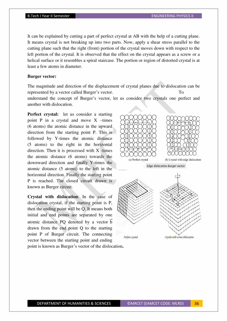
Burger vector:
The magnitude and direction of the displacement of crystal planes due to dislocation can be
represented by a vector called Burger’s vector. To
understand the concept of Burger’s vector, let us consider two crystals one perfect and
another with dislocation.
Perfect crystal: let us consider a starting
point P in a crystal and move X –times
(6 atoms) the atomic distance in the upward
direction from the starting point P. This is
followed by Y-times the atomic distance
(5 atoms) to the right in the horizontal
direction. Then it is processed with X -times
the atomic distance (6 atoms) towards the
downward direction and finally Y-times the
atomic distance (5 atoms) to the left in the
horizontal direction. Finally the starting point
P is reached. The closed circuit drawn is
known as Burger circuit.
Crystal with dislocation: In the case of
dislocation crystal, if the starting point is P,
then the ending point will be Q. It means both
initial and end points are separated by one
atomic distance PQ denoted by a vector b⃗ drawn from the end point Q to the starting
point P of Burger circuit. The connecting
vector between the starting point and ending
point is known as Burger’s vector of the dislocation.

B.Tech I Year II Semester ENGINEERING PHYSICS II
DEPARTMENT OF HUMANITIES & SCIENCES ©MRCET (EAMCET CODE: MLRD) 37
The Burger’s vector is perpendicular to the edge dislocation and is parallel to the screw
dislocation.
DIFFERENCES BETWEEN EDGE DISLOCATION AND SCREW DISLOCATION
S.N
o EDGE DISLOCATION SCREW DISLOCATION
1. Edge of an atomic plane is formed
internal to the crystal
Distortion of the lattice in the vicinity
of the screw dislocation takes place.
2. Tensile, compressive and shear stress
fields may be present. Only shear stress field.
3. It is perpendicular to the Burger's vector. It is parallel to its Burger's vector.
4. Edge dislocation moves in the direction of
the Burger vector.
It moves perpendicular to the Burger
vector.
5. Involves an extra row of atoms above or
below the slip plane.
Distortion follows a helical path either
right hand or left hand.
6. Force required to form and move an edge
dislocation is small.
Larger forces are required to form and
move screw dislocations.

B.Tech I Year II Semester ENGINEERING PHYSICS II
DEPARTMENT OF HUMANITIES & SCIENCES ©MRCET (EAMCET CODE: MLRD) 38
UNIT III DIELECTRIC PROPERTIES
Introduction:
All dielectric materials are insulators but all insulators are not perfect dielectric
materials. There are no free charges available for conduction in a dielectric. All the electrons
are tightly bound to their nucleus of the atoms. When the dielectric is placed in an electric
field, then separation of positive and negative charges takes place in a dielectric, causing
polarization of dielectric. Dielectrics are characterized by polarization & dielectric
constant.Dielecctrics materials store large amounts of electro-static fields. There are two
principal methods by which a dielectric can be polarized: stretching and rotation. Stretching
an atom or molecule results in an induced dipole moment added to every atom or molecule.
Rotation occurs only in polar molecules — those with a permanent dipole moment like the
water molecule shown in the diagram below.
Basic Definitions:
(1)Electric Dipole: Two opposite charges of equal magnitude separated by a finite distance
constitutes an electric dipole.

B.Tech I Year II Semester ENGINEERING PHYSICS II
DEPARTMENT OF HUMANITIES & SCIENCES ©MRCET (EAMCET CODE: MLRD) 39
(ii) Dipole moment(µ): Electric dipole moment is definis equal to product of one of the
charges and the charge separating distance.
Units: c-m or Debye, 1 Debye =3.3 × 10
-30 c-m
(iii) Permittivity (ε): Permittivity represents the easily polar sable nature of the dielectric or
medium.
o= permittivity of free space=8.854×10⁻¹²
F/m
(iv)Dielectric constant(εr): Dielectric constant is the ratio between the permittivity of the
medium and the permittivity of free space.
Let us take a parallel plate capacitor.
Suppose the separation distance between the
plates is d. Use air or vacuum as a medium for
this experiment.
Suppose +Q is the charge on one plate
and –Q is charge on the second plate. Bring a
rectangular slab made up of conducting material
between the plates of the capacitor. The thickness of the slab must be less than the distance
between the plates of the capacitor. When the electric field will be applied then polarization
of molecules will be started. The polarization will take place in the direction same as that of
electric field. Consider a vector that must be polarized, name it as P. The polarization vector
must be in the direction of electric field Eo. Then this vector will start its functioning and will
produce an electric field Ep in the opposite direction to that of Eo. The net electric field in
the circuit is shown by the figure. εr = ε/εo
E= Eo – Ep
Dielectric constant, property of an electrical insulating material (a dielectric) equal to the
ratio of the capacitance of a capacitor filled with the given material(c) to the capacitance of
an identical capacitor (co) (in a vacuum without the dielectric material. 𝜺 = / 𝟎
(v) Dielectric polarization (p): Diectric polarization or Electric polarization is the induced
dipole moment (µ) per unit volume (v) of the dielectric in the presence of an electric field.
Electric polarization, slight relative shift of positive and negative electric charge in opposite
directions within an insulator, or dielectric, induced by an external electrical field.
P = µ/v
Units: c-m-2
If “µ” is the average dipole moment per molecule and “N” is the number of

B.Tech I Year II Semester ENGINEERING PHYSICS II
DEPARTMENT OF HUMANITIES & SCIENCES ©MRCET (EAMCET CODE: MLRD) 40
molecules per unit volume then
P = N µ
(vi) Dielectric polarisability (α): Di-electric polarisability is the net dipole moment induced
per unit applied electric field.
P = N µ = N αE
Units: F-m2
(vii)Electric susceptibility (χ): It measures the the amount of polarization in a given electric
field produced in a dielectric. Polarization proportional to the product of ‘ o’ and applied
electric field
Χ = p/ oE
(viii)Electric flux density or Electric displacement (D): It is defined as the total number of
electric lines of force passing through the dielectric material is known as electric flux density
(D).
Mathematically it is represented by the following equation
D= oE + p
εE = oE + p
ε = oεr
oεrE = oE + p
p= oE(εr-1)
Types of polarization mechanisms in dielectrics:
There are four types of polarization processes in dielectric.
1. Electronic –polarization(pe)
2. Ionic – polarization(pi)
3. Orientation-polarization or di-polar polarization(po)
4. Space-charge polarization(ps)
1.Electronic –polarization(pe) or Atomic Polarization:
It is defined as polarization of rare-gas atoms in presence of an static electric field or
polarization due to displacement of an electron-cloud from positive charge of nucleus in an
atom in the presence of an electric field in a dielectric material is known as electronic-
polarization(pe). This involves the separation of the centre of the electron cloud around an
atom with respect to the centre of its nucleus under the application of electric field
2. Ionic – polarization(pi):
The polarization that occurs due to relative displacement of ions of the molecules in
the presence of an external electrical field. This happens in solids with ionic bonding which
automatically have dipoles but which get cancelled due to symmetry of the crystals. Here,
external field leads to small displacement of ions from their equilibrium positions and hence
inducing a net dipole moment. Ex: Nacl molecule

B.Tech I Year II Semester ENGINEERING PHYSICS II
DEPARTMENT OF HUMANITIES & SCIENCES ©MRCET (EAMCET CODE: MLRD) 41
Expression for Electronic polarization of a dielectric material:
The displacement of the positively charged nucleus and the (negative) electron of an
atom in opposite directions, on application of an electric field, result in electronic
polarization.
On application of external electric field E, the electron cloud around the nucleus
readily shifts towards the positive end of the field. Because of this, dipole moment is created,
within each atom due to the separation of positive and negative charges. This separation or
shift is proportional to field strength (E).
∴ Dipole moment is the product of charge and the separation between the charges.
∴ Induced dipole moment 𝜇 ∝
𝜇 =
αe is constant of proportionality or electronic polarizability and it is independent of
temperature.
Calculation of Electronic polarizability:
By taking classical model of an atom, the nucleus of change Ze is surrounded by an
electron cloud of charge –Ze distributed in a sphere of radius R.
Then the charge density (Z – atomic number) is given by
= − = − ( ) →
When an external electric field E is applied, the nucleus and electrons experience
Lorentz forces of magnitude ZeE in opposite direction. Because of this, the nucleus and
electron cloud are pulled apart. If separation is there in between nucleus and electron cloud, a
coulomb force develops which is attractive.
When Lorentz and Coulomb force are equal and opposite, equilibrium is reached.
Let ‘x’ be the displacement under this condition. Here, nucleus is much heavier than
the electron cloud; it is assumed that only the electron cloud is displaced when the external
field is applied.
Lorentz force = −
= × 𝑖 𝑖 𝜋𝜖
The charge enclosed =

B.Tech I Year II Semester ENGINEERING PHYSICS II
DEPARTMENT OF HUMANITIES & SCIENCES ©MRCET (EAMCET CODE: MLRD) 42
= − = (− ) = −
Coulomb force = × − × 𝜋𝜖 = −𝜋𝜖 In the equilibrium position,− = − 𝜖
= 𝜋𝜖
Thus, displacement of electron cloud is proportional to applied field
∝
The electric charges +Ze and –Ze are separated by a distance x under the influence of E
constituting induced dipoles (moment).
Induced electric dipole moment,
𝜇 =
= . 𝜋𝜖
= 𝜖
i.e. 𝜇 =
` where = 𝜖 is called electronic polarizability
It is the dipole moment per unit volume & is independent of temperature.
= 𝜇
= (where, N is the no. of atom/m3)
` = 𝜖 𝜖 − =
𝜖 − = 𝛼𝑒𝜖
, = 𝜖 𝜖𝑟−
Expression for Ionic polarization of a molecule:
The ionic polarization is due to the displacement of cation
and anions in opposite direction and occurs in an ionic solid.
Consider an electric field is applied in the positive x
direction then the positive ions move to the right by x1 and the
negative ions move to left by x2. If we assume, each unit cell has
one cation and one anion.
The resultant dipole moment per unit cell due to ionic
displacement is
𝜇 = +
If 1 and 2 are restoring force constants of cation and anion, Newton is the force due
to applied field. Then
= = , =

B.Tech I Year II Semester ENGINEERING PHYSICS II
DEPARTMENT OF HUMANITIES & SCIENCES ©MRCET (EAMCET CODE: MLRD) 43
Restoring force constants depends upon the mass of the ion and angular frequency of
the molecule in which the ions are present. = 𝜔 & = 𝜔
where m - mass of the positive ion & M-mass of the negative ion + = 𝜔 +
𝜇 = + = 𝜔 +
𝑖 = 𝜇 = 𝜔 +
The polarizability 𝑖 is inversely proportional to the square of natural frequency of the ionic
molecule and to its reduced mass which is equal to + −
Internal fields in solids [Lorentz Method]:
Now a dielectric material is placed between the
two parallel plate capacitor and there be an imaginary
spherical cavity around the atom ‘A’ inside the
dielectric. By taking that the radius of the cavity is
large compared to the radius of the atom. Now, the
internal field at the atom site ‘A’ can be considered to
be made up of four components namely E1, E2, E3 and
E4
Field E1: - E1 is the field intensity at A due to the
charge density on the plates
From the field theory. = 𝜖
= + 𝜖
∴ = 𝑃+𝜖𝜖
∴ = + 𝑃𝜖 →
Field E2: -
E2 is the field intensity at A due to charge density induced on the two sides of the
dielectric
Therefore = −𝜖 →

B.Tech I Year II Semester ENGINEERING PHYSICS II
DEPARTMENT OF HUMANITIES & SCIENCES ©MRCET (EAMCET CODE: MLRD) 44
Field 𝑬 :-
E3 is the field intensity at A due to other atoms contained in the cavity. If we assume a
cubic structure then E3=0 because of symmetry.
Field𝑬 :
E4 is the field density due to polarization charges on the surface of the cavity and it is
calculated by Lorentz. The enlarged view of the cavity is shown.
If dA is the surface area of the sphere of radius r lying between θ and θ+dθ
(where θ is the direction with reference to the direction of the applied force)
Then = 𝑖 θ = PQr => = 𝑖 θ θ = QRr ⟹ QR = rdθ
Hence, = 𝑖 θ θ
= 𝑖 θdθ
The charge dq on the surface dA is equal to the
normal component of the polarization multiplied by
the surface area. = 𝜃 =𝑖 𝜃 𝜃 𝜃
Field due to this charge at the centre ‘A’ is denoted by dE4 and is obtained by imagining a
unit charge at point ‘A’ = × × 𝜃𝜖
= 𝑖 𝜃 𝜃 𝜃 𝜃𝜖
= 𝜖 𝜃 𝑖 𝜃 𝜃 →
Thus, the total field E4 due to the charges on the surface of the entire cavity is obtained by
integrating ∴ ∫ = 𝜖 ∫ 𝜃𝜋 𝑖 𝜃 𝜃
= 𝜖 ∫ 𝜃𝜋 − 𝜃
= − 𝜖 𝜃 𝜋 = − 𝜖 − − = 𝜖

B.Tech I Year II Semester ENGINEERING PHYSICS II
DEPARTMENT OF HUMANITIES & SCIENCES ©MRCET (EAMCET CODE: MLRD) 45
i.e.
𝑖 = + 𝜖 →
where 𝑖 is the internal field (or) Lorentz field.
Clausius – Mosotti relation: -
The relation between the dielectric constant and the polarizability of a polarized
dielectric is known as Clasius – Mosotti equation. Consider the dielectric having cubic
structure, here there are no ions and permanent dipoles in these materials, the ionic
polarizability 𝑖 and orientational polarizability are zero.
i.e. 𝑖 = =
Polarization = 𝑖 = ( + 𝜖 )
− 𝛼𝜖 = = 𝛼𝑒− 𝛼𝜖 →
We have, = + 𝜖
= − 𝜖
𝑃 = − 𝜖
= 𝜖 − 𝜖
= 𝜖 𝜖 − 𝜖
∴ = 𝜖 𝜖 − →
Using (1) and (2): = 𝜖 𝜖 − = − 𝜖
− 𝜖 = 𝜖 𝜖 −
= 𝜖 ( + 𝜖 − )
⟹ 𝜖 = + 𝜖 −
= 𝜖 −𝜖 +
N is the no. of atoms by knowing 𝜖 , we can determine

B.Tech I Year II Semester ENGINEERING PHYSICS II
DEPARTMENT OF HUMANITIES & SCIENCES ©MRCET (EAMCET CODE: MLRD) 46
Piezoelectricity:
The material which is polarized when subjected to mechanical deformation is called
piezoelectric material. Piezoelectric materials are very important since they permit the
conversion of the mechanical energy into electrical energy and the process is reversible.
Example: Quartz, Barium Titanate [BaTio3] etc.
In Greek, Piezo (the term) means ‘pressure’ and it refers to the creation of opposite
kinds of charges at one pair of opposite faces of the piezo electric crystal when it is subjected
to mechanical compression. It is to develop the electrical energy through dielectric by the
application of mechanical force.
Inverse piezoelectricity:
When a d.c. power supply is connected across the electrical axis of the quartz crystal
then mechanical strain in the form of either expansion or contraction will be produced. This
phenomenon is known as Inverse – piezo electricity.
Instead, when A.c. electric field is applied across the electrical axis, then mechanical
vibration will be produced in the form of positive half cycle of a.c. field contraction takes
place and for the negative half cycle expansion takes place.
Piezoelectric materials and their applications:
Quartz crystal is very widely used for filter, resonator. And this crystal responds to
pressure variations ,so, it is used as pressure transducers
Rochelle salt is used as transducer in gramophone pick-ups, ear phones, hearing aids,
microphones etc.
Piezo electric semiconductors such as GaS, ZnO and CdS are finding applications as
amplifiers of ultrasonic waves.
The natural frequency of quartz crystal does not vary with temperature, using this
property, this crystal is used to produce highly stable RF oscillations for broadcasting
purposes and in quartz watches to maintain accurate time.
Ferro electricity:
The dielectric materials which are having spontaneous polarization in the absence of electric
field are called ferroelectric materials. And the phenomenon of possessing spontaneous
polarization in the absence of electric field is called ferroelectricity.
Properties:
1. All ferroelectric material possess spontaneous polarization
below a certain temperature.
2. As temperature increases the spontaneous polarization
decreases and at a particular temperature, the spontaneous
polarization vanishes. This temperature is known as Curie
temperature.

B.Tech I Year II Semester ENGINEERING PHYSICS II
DEPARTMENT OF HUMANITIES & SCIENCES ©MRCET (EAMCET CODE: MLRD) 47
3. Curie temperature can also be defined as the temperature at which ferroelectric material
coverts into para electric material.
4. Below curie temperature the dielectric constant depends on field strength. i.e., it is no
longer constant.
5. Above curie temperature dielectric constant varies with temperature according to curie –
wises law,
i.e., 𝜀 = −
𝑖 >
6. All ferroelectric materials exhibit the property of piezo electricity and pyro electricity.
7. The most important property of ferroelectrics is hysteresis under the action of an
alternating voltage.
Ex: - BaTio3, Lithium Niobate, Lithium Tantalate, etc.
HYSTERESIS:
When an electric field is applied on the ferroelectric
specimen, the polarization increases non - linearly and
reaches saturation at a certain value of 𝑷 . The polarization
will not change even if E is increased further .When the
field is reduced to zero, then the value of polarization does
not return to zero a certain amount of polarization called
remanent polarization 𝑷 , is still present in the material.
To remove this polarization, a electric field 𝑬 known as
coercive field must be applied in the opposite direction.
The shape of the hysteresis loop changes with temperature.
The height and width of the hysteresis decreases with
increase of temperature.
At certain temperature, the loop merges into a
straight line. This temperature is known as
ferroelectric curie temperature and the ferroelectric
behavior of the material disappears.
The hysteresis loop area represents the dielectric loss
that occurs in dielectric materials.
The spontaneous polarization of the ferroelectric material
depends upon
Shape of the hysteresis loop.
Dimensions of the specimen and temperature.
The thermal and electrical properties of the crystal.

B.Tech I Year II Semester ENGINEERING PHYSICS II
DEPARTMENT OF HUMANITIES & SCIENCES ©MRCET (EAMCET CODE: MLRD) 48
Applications of Dielectric materials:
1. Almost any type of electrical equipment employs dielectric materials in some form or
another.
2. Wires and cables that carry electrical current, for example, are always coated or wrapped
with some type of insulating (dielectric) material.
3. Quartz crystal is used for the preparation of ultrasonic transducers, crystal oscillators,
delay lines, filters, etc...
4. Barium Titanate is used for preparation of accelerometer.
5. Lead Zinconate titanate is used to preparation of earphones, microphones, spark
generators.
6. The Insulating dielectric liquids are used in transformers, switch gears and generators. It's
also used in radiation detectors, Thermo ionic valves, strain gauges, capacitors, resistors
and many other Electric devices.
7. The electro optic devices are prepared using dielectric materials.

B.Tech I Year II Semester ENGINEERING PHYSICS II
DEPARTMENT OF HUMANITIES & SCIENCES ©MRCET (EAMCET CODE: MLRD) 49
UNIT IV MAGNETIC PROPERTIES
Introduction:
Magnetism has its own application in the field of physics. Magnetic properties have
been the subject of special interest because of the information they yield about the
constitution of matter. Magnetics have wide range of application in electrical machinery and
in magnetic tapes in computers. Magnetic materials are classified into three, namely
diamagnetic, paramagnetic and ferromagnetic materials.
Magnetic field: The 3D region around a magnet in which it`s magnetic force is felt is called
magnetic field of that magnet. It is a scalar quantity.
Magnetic dipole: It`s a system consisting of two equal and opposite magnetic poles
separated by a small distance of
Or
Two poles of equal strength separated by a very small distance is
called a magnetic dipole.
Pole strength (m): The ability of a pole of magnet to attract or repel another magnetic pole
is called it`s pole strength.
Magnetic dipole moment (𝛍): It can define in three ways depending on situation.
1. In case of bar magnet it is defined as the product of pole strength and distance
between them.
𝜇 =
2. In case of current carrying conductor, it is the product of current (i) and cross section
area (A) of the conductor.
𝜇 = 𝑖 3. In case of atom, it is the product of current (i) developed by orbital motion of electron
and the area covered by the orbital.
𝜇 = 𝑖
It is a vector quantity. Its direction is from south pole to the north pole.
Its SI unit is ampere m .⁄
Magnetic flux ∅ : The total number of magnetic lines of force passing normal to a surface
in a magnetic field is called magnetic flux.
Or
The number of magnetic lines of force passing through a point is called magnetic flux.
Its SI unit is weber or tesla − m
Magnetic field induction or magnetic flux density (B): The magnetic flux passing through
a unit normal area of substance is defined as magnetic flux density and is denoted by B. It is

B.Tech I Year II Semester ENGINEERING PHYSICS II
DEPARTMENT OF HUMANITIES & SCIENCES ©MRCET (EAMCET CODE: MLRD) 50
commonly known as magnetic induction. Let ∅ be the flux passing through a substance of
area A, then flux density is
= ∅ = 𝐫 ∅ = . = BA cos θ.
It is a vector quantity.
Its SI unit is weber m or tesla⁄ and CGS unit is Gauss(= ⁄ ).
1Tesla= Gauss.
Magnetising field(force) or Magnetic intensity(H): The force acting on a unit north pole
placed at the point. It is independent of the medium.
= 𝜇
It is vector quantity. Its SI unit is ampere m.⁄
Permeability: It`s ability to allow the magnetic lines of force to pass through it or to allow
itself to be influenced by magnetic field 𝜇).
Relative magnetic permeability 𝝁 :The ratio of its absolute magnetic permeability(µ) of
the material to the magnetic permeability of free space (µo).
𝜇 = 𝜇𝜇
It is purely a number, it has no units.
The permeability of free space or vacuum is = π × − H m⁄ .
Magnetization: The ability of a material to get magnetized when placed in an external
magnetic field is called magnetization.
It is measured by a quantity called intensity of magnetization I .
The net magnetic dipole moment acquired by a substance per unit volume is
defined as intensity of magnetization (I).
I = net magnetic dipole moment of materialVolume of the material A m⁄
It is vector quantity. Its SI unit is A m⁄ .
Relation between B,H and I:
The flux density B in a material due a to magnetizing force H, as the sum of the flux density
in vacuum produced by magnetizing force and flux density due to magnetization of
material.
Therefore = +
Also we know that = 𝜇 = 𝜇 I
Therefore, = 𝜇 + 𝜇 I

B.Tech I Year II Semester ENGINEERING PHYSICS II
DEPARTMENT OF HUMANITIES & SCIENCES ©MRCET (EAMCET CODE: MLRD) 51
B = H + I
It is the relation in SI unit
Magnetic Susceptibility 𝝌 : The ratio of magnetization to the magnetic intensity.
𝝌 = I
It has no units when a material has high susceptibility then it can be easily magnetized.
Relation between Permeability and Susceptibility:
We know that B ∝ (H+I)
B = µo (H+I)
In vacuum B = µo H + µo I
= 𝜇 + 𝜇
Also, = 𝜇
permeability of the material and
χ = I Susceptibility
∴ 𝜇 = µo + µo χ or 𝜇 = µo + χ 𝜇𝜇 = + χ
𝜇 = + χ 𝜇 −1 = χ 𝜇 = χ +
Origin of magnetic moment: Materials are made up of atoms. These atoms consist of positively charged
nucleus, surrounded by cloud of electrons. In all atoms electrons are revolving around the
nucleus in different orbits and also spin about their own axis. These revolving electrons
constitute an electrical current in the orbits. These revolving electrons produces its own
orbital magnetic dipole moment, measured in Bohr magneton 𝜇 and there is also a spin
magnetic moment associated with it spin of orbital electrons and spin of nucleus .In
most materials there is no resultant magnetic moments, due to the electrons being grouped in
pairs causing the magnetic moment to be cancelled by its neighbour. Under external applied

B.Tech I Year II Semester ENGINEERING PHYSICS II
DEPARTMENT OF HUMANITIES & SCIENCES ©MRCET (EAMCET CODE: MLRD) 52
magnetic field these dipoles experience torque in the direction of applied field and the atom
acquires certain magnetism. So, the magnetic moment of an atom is due to
1. Orbital magnetic moment of the electrons.
2. Spin magnetic moment of the electrons.
3. Spin magnetic moment of the nucleus.
The orbital magnetic moment of the electrons 𝐫 𝐌𝐚 𝐞𝐭 :
The magnetic moment contributed by a single electron is known as Bohr Magneton.
Mathematically it can express as
𝜇 = ℏ
Proof:
Let us consider an electron revolving in a circular orbit of radius r with a speed 𝒗 .Consider a
point p on the circle. The electron crosses this point once in every revolution. In one
revolution the electron travels 2 r distance.
The current 𝒊 due to the electron motion in the circular loop (orbit) is
𝒊 = ℎ 𝑖 = −
Where, T is time for one revolution of electron about the nucleus.
T = 𝑖 =
𝜋
𝒊 = −[ 𝜋𝑟𝑣 ] = −𝜋r
The magnetic moment 𝜇 associated with the orbit due to orbital motion of electron is
𝜇 = 𝑖
Where, ’ 𝒊’ is current produced by the
orbital motion of the electron and A is area covered by the orbital πr .
𝜇 = − r ×
Dividing and multiplying above eq. by the mass of the electron
𝜇 = − × =
− [ ]

B.Tech I Year II Semester ENGINEERING PHYSICS II
DEPARTMENT OF HUMANITIES & SCIENCES ©MRCET (EAMCET CODE: MLRD) 53
= −m [ ]
w.k.t the angular momentum of an electron revolving in circular orbit is equal to integral
multiple of ℎ π = = ℎ 𝜇 = ( − ℎ m) 𝜇 = 𝜇 where l= 0,1,2........
Where, l = orbital quantum number. 𝜇 = − ℎ m
Bhor magneton = . × − × . × −× . × . × − = . × − A – m
Here – sign indicates that magnetic moment is anti parallel to the angular momentum L.
Spin magnetic moment of the electrons:
In addition to orbital motion, the electron spins around its own axes. The magnetic moment
due to spin of electron is represented as 𝜇s 𝜇s = ℎ π
The factor 2 is due to the variation in the moment of inertia.
W k t = ± 𝜇s = ћ 𝜇 = 𝜇
Spin magnetic moment of the nucleus: The nucleus of the atom posses nuclear spin hence magnetic moment is associated with this.
The nuclear magnetic moment is expressed in the units of nuclear magneton (𝜇n) 𝜇 = eћ mp = 5.05× 10
-29 A – m
2
Where , mp - mass of the proton.

B.Tech I Year II Semester ENGINEERING PHYSICS II
DEPARTMENT OF HUMANITIES & SCIENCES ©MRCET (EAMCET CODE: MLRD) 54
CLASSIFICATION OF MAGNETIC MATERIAL:
Depending on the direction and magnitude of magnetization and also the effect of
temperature on magnetic properties, all magnetic materials are classified into dia , para and
ferro materials.Depending upon the spin orientation of the electrons, ferro magnetic
materials are classified into two types. They are
a. Antiferro magnetic material.
b. Ferrimagnetic materials.
PROPERTY DIA MAGNETIC
SUBSTANCES
PARA MAGNETIC
SUBSTANCES
FERRO MAGNETIC
SUBSTANCES
Defination
The substance in
which the resultant
magnetic moment of
individual atoms is
zero.
The substance in
which the resultant
magnetic moment of
individual atoms is
not zero.
The substance in which
the resultant magnetic
moments of individual
atoms align themselves
in parallel by giving rise
to spontaneous
magnetization
Cause Orbital motion of
electrons.
Spin motion of
electrons. Formation of domains.
Susceptibility𝝌 Low and negative Low and positive. High and positive.
𝝌 depend on T Does not depend on T.
except Bi at low T.
χ = (curie law)
c is curie constant.
𝜒 = − 𝑐 : >
(curie wises law)
Tc is curie temperature.
𝝌 depend on H Does not depend Does not depend Does not depend
Relative
permeability
µr)
<1 >1 1
I
It`s direction is
opposite to that of H
and value is very low.
It`s in direction of H
and value is high.
It`s in direction of H and
value is very high.
spin alignment No spin alignment is
present.
All spins or magnetic
moments are
randomly oriented.
All spins or magnetic
moments are orderly
oriented.

B.Tech I Year II Semester ENGINEERING PHYSICS II
DEPARTMENT OF HUMANITIES & SCIENCES ©MRCET (EAMCET CODE: MLRD) 55
Antiferro magnetic materials:
These are the ferromagnetic materials in which the magnetic interaction between any
two dipoles aligns themselves anti parallel to each other. All the dipoles are equal in
magnitude. Therefore the resultant magnetization is zero.
I-H curve.
𝝌 – T curve
Transition of
material at Tc Do not change.
On cooling these are
converted into
ferromagnetic
material.
Converted into
para magnetic material
above Tc.
Nature of
effect. Distortion effect. Orientation effect. Hysteresis effect.
In the presence
of magnetic
field.
The magnetic lines of
force are pulled out
from the material
.Hence, magnetic flux
density is greater,
outside the material
than inside.
The magnetic lines of
force are attracted
towards the centre of
the material and hence
the Bin material is
greater than the B out.
The magnetic lines of
force are highly attracted
towards the centre of the
material and hence the
Bin material is very
greater than the B out.
Example: Bi, Zn, H2O, Gold..... Al, Pt, Mn , cucl2.... Fe, Ni, Co, Mno,
Fe2o3....

B.Tech I Year II Semester ENGINEERING PHYSICS II
DEPARTMENT OF HUMANITIES & SCIENCES ©MRCET (EAMCET CODE: MLRD) 56
Properties:
1. Susceptibility is small and positive for these materials.
2. Spin alignment is systematic, but in anti parallel manner.
3. Initially, the susceptibility increases slightly as the
temperature increases, and beyond a particular temperature
known as Neel temperature the susceptibility decreases with
temperature.
4. The temperature at which anti ferromagnetic material
converts into paramagnetic material is known as Neel`s
temperature.
5. Susceptibility is inversely proportional to the temperature.
The variation of susceptibility with temperature is expressed
as
𝜒 = + When T > TN 𝜒 ∝ When T < TN
Where ‘c’ is the curie constant and the is Neel temperature.
Ex: FeO, MnO, Cr2O3
Ferrimagnetic materials: These are the ferromagnetic materials in which the magnetic
interaction between any two dipoles align themselves anti parallel to
each other. But the magnitudes of any two adjacent dipoles are not
equal. Therefore, if we apply a small value of magnetic field, it will
produce a large value of magnetization.
Properties:
1. Susceptibility is positive and very large for these materials.
2. Spin alignment is systematic, but in anti parallel of different
magnitudes.
3. Ferrimagnetic materials possess net magnetic moment.
4. Above curie temperature becomes paramagnetic while below it
behaves as ferrimagnetic material.
5. Ferrimagnetic domains become magnetic bubbles to act as
memory elements.
6. Susceptibility is inversely proportional to the temperature. The
variation of susceptibility with temperature is
𝜒 = ±
>
Where, C is curie constant and is Neel temperature.
7. Ferrites are the best examples of ferromagnetic materials.
8. General formula of ferrites are Me2+
OFe2O3 or Me2+
Fe2O4
Examples: Zn2+
Fe2O4, CuFe2O4.......

B.Tech I Year II Semester ENGINEERING PHYSICS II
DEPARTMENT OF HUMANITIES & SCIENCES ©MRCET (EAMCET CODE: MLRD) 57
HYSTERESIS CURVE:
It means retardation. [or] Lagging of an effect behind the cause of the effect [or] The
phenomenon of B lagging H. [or] It is also defined as a phenomenon of flux density (B) with
the change in magnetic field strength (H) in a ferromagnetic material.
Explanation: When the magnetic field H is applied on an un magnetized ferromagnetic
material the magnetic induction increases first rapidly and then slowly from o to a. The
increase is non linear, after that the rate of induction slows down and attaining a saturation
value Bsat, with further increase in H , there is no increase in B.If applied magnetic field H on
the material is decreased at this stage, naturally B decreases and B will not travel in that
initial path, creates a new path.
When H is reduced to zero, B does not vanish , the value
of B that remains in the material is called as retentivity Br or
reduce magnetisation. To remove retentivity in the material
sufficient negative magnetic field –Hc or Hc is applied in
opposite direction then the retentivity Br becomes zero .This is
(field) known as coherceive field. On increasing H further B
reaches saturation in the opposite direction denoted by ’c’. Then reducing H to zero B reaches ‘d’ and then increasing H in
the positive direction B reaches again to Bsat and a curve is
obtained. This completes a closed loop called hysteresis loop.
It includes some area. This area indicates the amount of energy
wasted in one cycle of operation.
Domain Theory of Ferromagnetism:
The concept of domains was proposed by Weiss in order to
explain the properties of ferromagnetic materials and their
hysteresis effects.
Magnetic Domains: Every ferromagnetic material is made of a
very large number of miniature (very small) regions which are
known as domains. The boundaries separating the domains are
called domain walls, also known as Bloch walls.
In each domain the magnetic dipoles align parallel to each
other and produce spontaneous magnetization. The direction of spontaneous magnetization
varies from domain to domain.
Process of Domain magnetization:
When the external field is applied there are two possible ways of alignment of random
domains.
1. By the motion of domain walls.
2. By rotation of domains.
Motion of Domain walls: When a small amount of magnetic fieldis applied on a ferro
magnetic material then the domains of the material whose magnetic moments are parallel or
nearly parallel to the direction of applied field can grow in size where as the domains are not

B.Tech I Year II Semester ENGINEERING PHYSICS II
DEPARTMENT OF HUMANITIES & SCIENCES ©MRCET (EAMCET CODE: MLRD) 58
parallel to field can diminish in size. This change produces large magnetization for the bulk
materi
Rotation of Domains:
When the magnetic field is increased further to a large
value i. e. , near saturation , further domains growth becomes impossible and hence fully
grown domains can rotate into the field direction and specimen is said to be saturated.
SOFT AND HARD MAGNETIC MATERIALS:
Ferromagnetic materials are classified into two types based on the characteristic parameters
such as hystersis and magnetisation. They are
1. Hard magnetic materials
2. Soft magnetic materials
S.NO SOFT MAGNETIC MATERIAL HARD MAGNETIC MATERIAL
1
Materials which can be easily
magnetized and demagnetized are
called Soft magnetic materials.
Materials which can’t be easily
magnetized and demagnetized are
called hard magnetic materials.
2
The nature of hysteresis loop is very
steep
The nature of hysteresis loop is very
large.
3 They are prepared by annealing
process.
They are prepared by quenching
process.
4 Due to small hysteresis loop area,
they have small hysteresis loss.
Due to large hysteresis loop area, they
have large hysteresis loss.
5 They have large value of
permeability and susceptibility.
They have low value of permeability
and susceptibility.
6 The coercivity and retentivity are
small.
The coercivity and retentivity are
large.
7 They are free from irregularities. They have large amount of impurities
and lattice defects.
8 They are used
To produce temporary magnets.
They are used
To produce permanent magnets.

B.Tech I Year II Semester ENGINEERING PHYSICS II
DEPARTMENT OF HUMANITIES & SCIENCES ©MRCET (EAMCET CODE: MLRD) 59
In the preparation of magnetic
core materials used in
transformers, electric motors ,
magnetic amplifiers, magnetic
switching circuits, etc.,
In loud speakers, toys, in
measuring meters, microphones,
magnetic detectors, magnetic
separators, etc.,
9 Ex: Iron and silicon alloys ,Nickel –
Iron alloy, Iron – Cobalt alloy.
Ex: High carbon steel, Cobalt steel,
Barium ferrite .

B.Tech I Year II Semester ENGINEERING PHYSICS II
DEPARTMENT OF HUMANITIES & SCIENCES ©MRCET (EAMCET CODE: MLRD) 60
SUPER CONDUCTIVITY
Introduction: Certain metals & alloys exhibit almost zero resistivity (infinite
conductivity), when they are cooled sufficiently to low temperature is known as Super
conductivity.
Super conductivity has got important applications like energy fields, energy technology, tele
communications, computing, super fast transportation, medicine e.t.c
General properties:
The temperature at which the transition from normal stage to the Super conducting stage
takes place on cooling in the absence of magnetic field is called critical temperature (TC )
is also known as Transition temperature.
H.K onnes by studying the electrical conductivity of metals he came across this
phenomenon. He found that when pure mercury was cooled down below 40
K the resistivity
suddenly dropped to zero. A similar behavior is observed in case of metal ‘tin’ the sudden
drop in resistivity is graphically shown below.
Properties observed:
1. TC is different for different substances.
2. For chemically pure & structurally perfect Super conducting transition is very sharp.
3. Super conductivity substance in general lies in the inner column of periodic table.
4. Super conductivity is found in metallic substance in which the valence electron no
lies in between 2&8.
5. From the periodic table it is observed that (TC ) of the elements &square of atomic
no (Z2) are having direct proportionality relation .
6. Transition metals having odd no of electrons exhibit Super conductivity.
7. Materials having high normal resistance exhibit Super conductivity.
8. Super conductivity is also observed in a substances having in all atomic volume with
small atomic mass.
9. Ferro &anti Ferro magnetic substances do not exhibit Super conductivity.
10. In addition to dropping of electrical resistivity to zero the following changes are also
observed.
a) The magnetic flux lines are rejected from the super conductor is known
“MEISSNER EFFECT” .
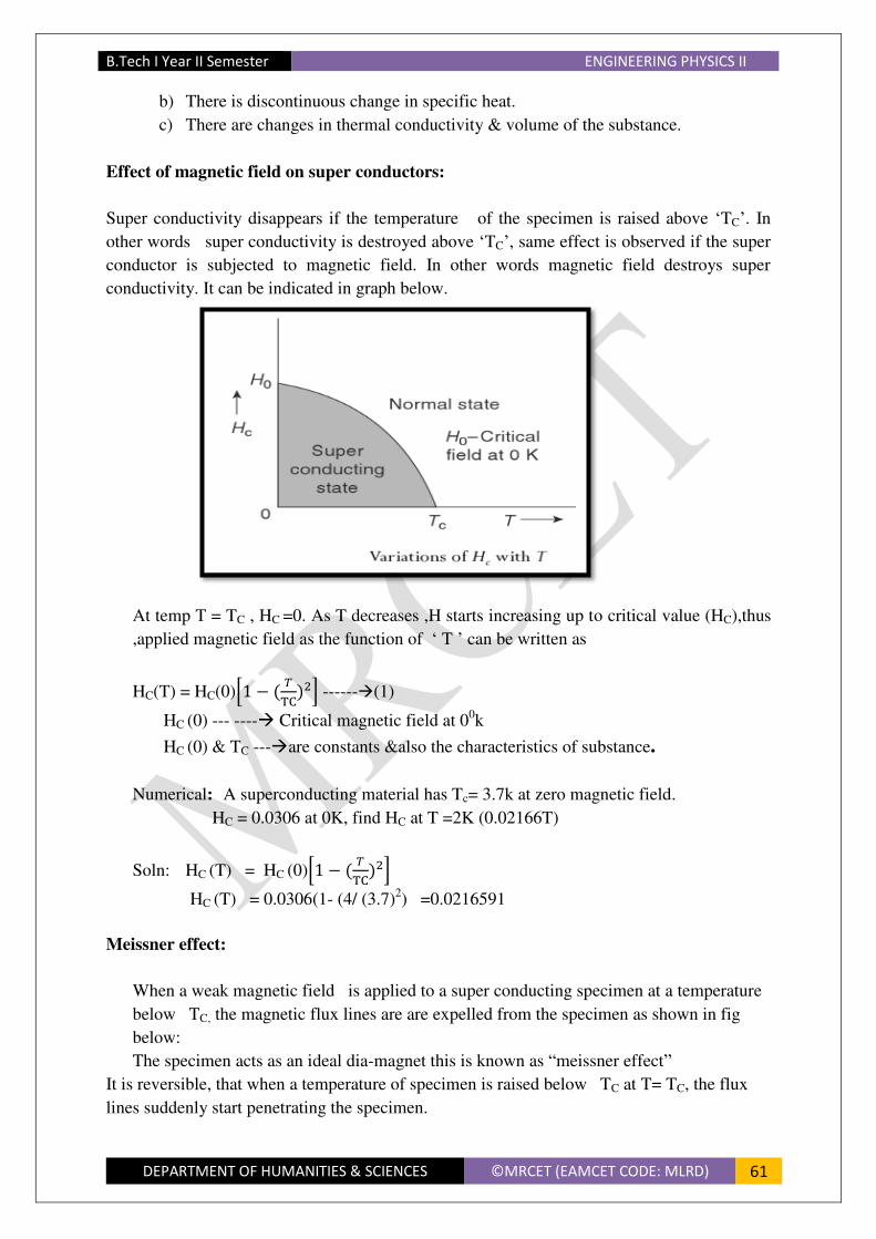
B.Tech I Year II Semester ENGINEERING PHYSICS II
DEPARTMENT OF HUMANITIES & SCIENCES ©MRCET (EAMCET CODE: MLRD) 61
b) There is discontinuous change in specific heat.
c) There are changes in thermal conductivity & volume of the substance.
Effect of magnetic field on super conductors:
Super conductivity disappears if the temperature of the specimen is raised above ‘TC’. In
other words super conductivity is destroyed above ‘TC’, same effect is observed if the super
conductor is subjected to magnetic field. In other words magnetic field destroys super
conductivity. It can be indicated in graph below.
At temp T = TC , HC =0. As T decreases ,H starts increasing up to critical value (HC),thus
,applied magnetic field as the function of ‘ T ’ can be written as
HC(T) = HC(0)[ − T ] ------(1)
HC (0) --- ---- Critical magnetic field at 00k
HC (0) & TC ---are constants &also the characteristics of substance.
Numerical: A superconducting material has Tc= 3.7k at zero magnetic field.
HC = 0.0306 at 0K, find HC at T =2K (0.02166T)
Soln: HC (T) = HC (0)[ − T ] HC (T) = 0.0306(1- (4/ (3.7)
2) =0.0216591
Meissner effect:
When a weak magnetic field is applied to a super conducting specimen at a temperature
below TC, the magnetic flux lines are are expelled from the specimen as shown in fig
below:
The specimen acts as an ideal dia-magnet this is known as “meissner effect”
It is reversible, that when a temperature of specimen is raised below TC at T= TC, the flux
lines suddenly start penetrating the specimen.

B.Tech I Year II Semester ENGINEERING PHYSICS II
DEPARTMENT OF HUMANITIES & SCIENCES ©MRCET (EAMCET CODE: MLRD) 62
The specimen comes back to normal stage, under these conditions magnetic induction of a
specimen B=µ0 (H+I) --- (2) where, H---- applied magnetic field.
µ ---- magnetization.
As , B=0 ; µ0 (H+I) =0 --(3)
H = -I;
ᵪ = = − . Hence susceptibility is -1, the substances are diamagnetic.
In case of super conductor resistivity (ρ =0), But electric field, = J ρ ---- (4) == =0.
Also from DEL*E = =-- = ; so, B should be constant.
This contradicts meissner effect itself.
Hence we can say that, super conducting substance or specimen behave differently from
that of normal specimen. Ultimately, in super conducting stage E=0, & B=0
Effect of current:
To destroy the super conducting property critical magnetic field (HC) is required. As the
current is flowing through the super conductor the specimen can produce its own magnetic
field if superconductivity is to be destroyed. In other words if the current in the specimen is
increased to critical value IC .So that HC is produced ,super conductivity disappears.
Hence , IC can be related as IC = 2∏r HC –-- (5)
Mathematically IC is related to HC & is clear from following example.
Numerical:
Calculate critical current passing through the wires having diameter1mm, at temp=4.2K, TC
for lead is 7.18k, value of H0=6.5*104
A/m.
Soln: HC = H0[ − T ] HC = 6.5*10
4 [ − .. ] = 42758.55246
IC = 2∏r HC = 2*3.14*1*42758.55246 =134.518A
Types of super conductors:
They can be classified as Type-1 & Type-2 depending on the exhibition of meissener
effect.

B.Tech I Year II Semester ENGINEERING PHYSICS II
DEPARTMENT OF HUMANITIES & SCIENCES ©MRCET (EAMCET CODE: MLRD) 63
Type-1 Super conductor : They also known as soft super conductors ,when the magnetic
field is applied & increased gradually from its initial value H<HC, the diamagnetism
disappears abruptly.
Super conducting specimen changes to normal state sharply as shown in fig. Al, zn, Hg are
eg, of Type-1 Super conductor.
Type-2 Super conductor: As shown in fig, Type-2 conductors are having two critical fields
namely H & H . Up to the field H the specimen is in pure super conducting state
rejecting all the magnetic lines. Beyond H lower critical field ,magnetic lines starts
penetrating the specimen ,up to the second critical field H upper critical field ,the
specimen is in mixed state .In other words in this region between H & H the
meissner effect is in complete .This region is “Vortex-region”. Beyond H the specimen
completely becomes normal from super conducting state. eg : Niobium (Nb) ,Zirconium (Zr)
They also known as Hard superconductors, these have large practical applications, since they
got very high current density.
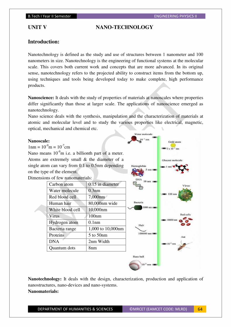
B.Tech I Year II Semester ENGINEERING PHYSICS II
DEPARTMENT OF HUMANITIES & SCIENCES ©MRCET (EAMCET CODE: MLRD) 64
UNIT V NANO-TECHNOLOGY
Introduction:
Nanotechnology is defined as the study and use of structures between 1 nanometer and 100
nanometers in size. Nanotechnology is the engineering of functional systems at the molecular
scale. This covers both current work and concepts that are more advanced. In its original
sense, nanotechnology refers to the projected ability to construct items from the bottom up,
using techniques and tools being developed today to make complete, high performance
products.
Nanoscience: It deals with the study of properties of materials at nanoscales where properties
differ significantly than those at larger scale. The applications of nanoscience emerged as
nanotechnology.
Nano science deals with the synthesis, manipulation and the characterization of materials at
atomic and molecular level and to study the various properties like electrical, magnetic,
optical, mechanical and chemical etc.
Nanoscale:
1nm = 10-9
m = 10-7
cm
Nano means 10-9
m i.e. a billionth part of a meter.
Atoms are extremely small & the diameter of a
single atom can vary from 0.1 to 0.5nm depending
on the type of the element.
Dimensions of few nanomaterials:
Carbon atom 0.15 in diameter
Water molecule 0.3nm
Red blood cell 7,000nm
Human hair 80,000nm wide
White blood cell 10,000nm
Virus 100nm
Hydrogen atom 0.1nm
Bacteria range 1,000 to 10,000nm
Proteins 5 to 50nm
DNA 2nm Width
Quantum dots 8nm
Nanotechnology: It deals with the design, characterization, production and application of
nanostructures, nano-devices and nano-systems.
Nanomaterials:
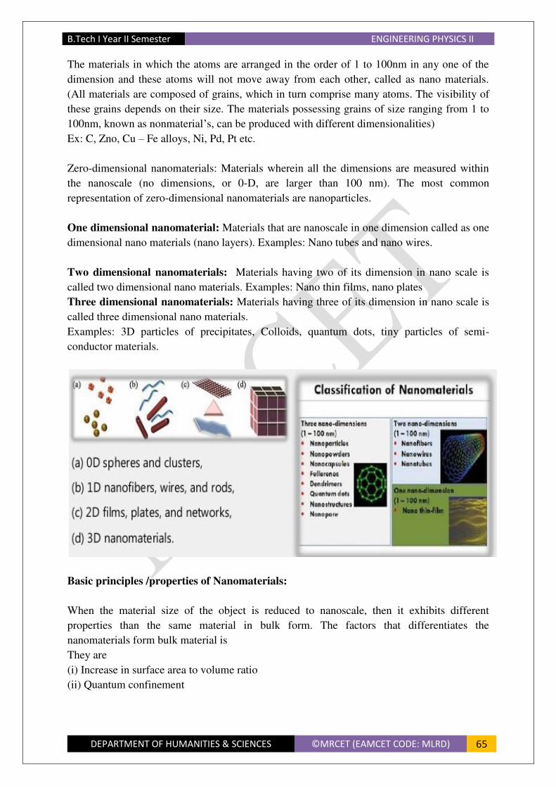
B.Tech I Year II Semester ENGINEERING PHYSICS II
DEPARTMENT OF HUMANITIES & SCIENCES ©MRCET (EAMCET CODE: MLRD) 65
The materials in which the atoms are arranged in the order of 1 to 100nm in any one of the
dimension and these atoms will not move away from each other, called as nano materials.
(All materials are composed of grains, which in turn comprise many atoms. The visibility of
these grains depends on their size. The materials possessing grains of size ranging from 1 to
100nm, known as nonmaterial’s, can be produced with different dimensionalities)
Ex: C, Zno, Cu – Fe alloys, Ni, Pd, Pt etc.
Zero-dimensional nanomaterials: Materials wherein all the dimensions are measured within
the nanoscale (no dimensions, or 0-D, are larger than 100 nm). The most common
representation of zero-dimensional nanomaterials are nanoparticles.
One dimensional nanomaterial: Materials that are nanoscale in one dimension called as one
dimensional nano materials (nano layers). Examples: Nano tubes and nano wires.
Two dimensional nanomaterials: Materials having two of its dimension in nano scale is
called two dimensional nano materials. Examples: Nano thin films, nano plates
Three dimensional nanomaterials: Materials having three of its dimension in nano scale is
called three dimensional nano materials.
Examples: 3D particles of precipitates, Colloids, quantum dots, tiny particles of semi-
conductor materials.
Basic principles /properties of Nanomaterials:
When the material size of the object is reduced to nanoscale, then it exhibits different
properties than the same material in bulk form. The factors that differentiates the
nanomaterials form bulk material is
They are
(i) Increase in surface area to volume ratio
(ii) Quantum confinement

B.Tech I Year II Semester ENGINEERING PHYSICS II
DEPARTMENT OF HUMANITIES & SCIENCES ©MRCET (EAMCET CODE: MLRD) 66
Increase in surface area to volume ratio: Nano materials have a large surface area to
volume ratio when compared to bulk material and it is a great measure for efficiency of
nanotechnology.
Example: Let us consider a sphere of radius ‘r’ Its surface area = 4πr2
Its volume (atom)= 4/3 πr3
Surface area (S.A.) to volume ratio = 4πr2
43πr3
= 3
Therefore when the radius of the sphere decreases, its surface area to volume ratio increases.
Example: Let us consider a cubic volume shown
in figure.
If a given sample its surface area is 6m2. When it
is divided into 8 pieces its surface area becomes
12m2. When the volume is divided into 27 pieces
its surface area becomes 18m2.
Thus, when the given volume is divided into
smaller pieces, the surface area increases.
Due to increase in surface area, more number of
atoms will appear at the surface. This makes nano
materials more chemically reactive. Reducing the
dimensions of material affects reactivity, optical
properties, electrical properties, magnetic
properties.
(ii) Quantum Confinement: The properties of materials can be studied based on the energy
levels. When atoms are isolated, their energy levels are discrete. When very large no of atoms
are closely packed to form a solid, the energy levels split & form bands. Nano materials
represent intermediate stage. As a result, the energy levels change.
When we apply the problems of particles in a potential well as well as in a potential box. The
dimensions of such wells or boxes are of the order of deBroglie wavelength of electrons,
energy levels of electrons change. This effect is called Quantum confinement.
This affects the optical, electrical, magnetic properties of nanomaterials.
When the electrons are confined, the particles will have more oscillations and this will result
in colour change of the materials. For examples, nano gold colloids are dispersed in ruby
glass, the ruby glass exhibits red hue.
Synthesis (or) Fabrication of nanomaterials:
The production of nano materials or nano crystalline materials requires precise methods.
There are various techniques that are capable of creating nano structures. In general there are
two approaches that are classified as
1) Top-down approach (or) technique

B.Tech I Year II Semester ENGINEERING PHYSICS II
DEPARTMENT OF HUMANITIES & SCIENCES ©MRCET (EAMCET CODE: MLRD) 67
2) Bottom-up approach (or) technique
Top–down approach: Top down techniques involves starting with a block of individual
material, etching (removing the surface by dissolution) or convert it down to the desired size.
The challenge here is to produce smaller and smaller structures.Nano material particle can be
made through this method.
In this method, the nanomaterials are synthesized by assembling or arranging the bulk
materials into nanosizes.
Top –down processing has been and will be the dominant process in semiconductor
manufacturing.
Examples: (i) Sol-gel method.
(ii) Ball-milling method.
(iii) Lithography.
(iv)Mechanical grinding.
Bottom-up approach: Bottom-up technique involves the assembly of smaller sub unit
(atoms or molecules) to make larger structure.
In this method, the nano materials are synthesized by assembling (or) arranging the atoms or
molecules together to form the nano materials.
Examples: (i) physical vapour deposition method
(ii) Chemical vapour deposition method
(iii) Plasma arcing and
(iv) Electro deposition
Sol-Gel Method:
The sol-gel method is a wet chemical method or chemical solution deposition method. This
technique is used to generate nanoparticles & nanopowders.
A given material converted into colloids & dissolved in water or in acids, then forms a
solution (Sol). A colloid suspended in a liquid is called as “Sol”. A suspension that keeps its
shape is called Gelatin or “Gel”. The sol-gel formation occurs in different stages. They are
1) Hydrolysis of precursors.
2) Condensation and polymerization of monomers to form particles.
3) Growth of particles and development of particles. (Agglomeration)
The schematic representation of the synthesis of nano particles using the Sol-Gel method is
shown in fig.

B.Tech I Year II Semester ENGINEERING PHYSICS II
DEPARTMENT OF HUMANITIES & SCIENCES ©MRCET (EAMCET CODE: MLRD) 68
This method takes place in following steps.
(i) Take a material & convert it into liquid precursors (inorganic salts or organic species such
as
metal –alkoxide) & dissolved in water or in other solvents. It forms colloidal suspensions
known as “Sol”.
(ii)This solution is kept at a suitable temperature and some amounts of gelling agents are
added to it. This will produce a gel.( By dehydration reaction with Sol forms Gel )
(iii) Rapid drying of the gel, under super critical conditions an aero-gel.
(iv) Drying of the “Gel” i.e. water & other liquids are removed from the gel forms a Xerogel.
By calcination xerogel forms ceramics.
(V) The solution further proceed through spinning & finally by calcination forms thin films &
nanopowder respectively.
Advantages:
(i) This method is used to prepare thin films, nanopowder, glasses, glass ceramics etc at very
low temperatures.
(ii) To prepare mono-sized nanoparticles.
(iii)Very high purity in synthesized materials can be obtained.
Disadvantages:
(i) The raw materials are very costly.
(ii) The synthesis reaction requires relatively longer time.
(iii) Organic solvents used are harmful to the environment.
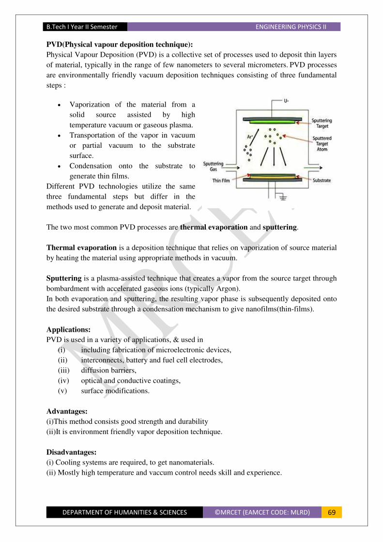
B.Tech I Year II Semester ENGINEERING PHYSICS II
DEPARTMENT OF HUMANITIES & SCIENCES ©MRCET (EAMCET CODE: MLRD) 69
PVD(Physical vapour deposition technique):
Physical Vapour Deposition (PVD) is a collective set of processes used to deposit thin layers
of material, typically in the range of few nanometers to several micrometers. PVD processes
are environmentally friendly vacuum deposition techniques consisting of three fundamental
steps :
Vaporization of the material from a
solid source assisted by high
temperature vacuum or gaseous plasma.
Transportation of the vapor in vacuum
or partial vacuum to the substrate
surface.
Condensation onto the substrate to
generate thin films.
Different PVD technologies utilize the same
three fundamental steps but differ in the
methods used to generate and deposit material.
The two most common PVD processes are thermal evaporation and sputtering.
Thermal evaporation is a deposition technique that relies on vaporization of source material
by heating the material using appropriate methods in vacuum.
Sputtering is a plasma-assisted technique that creates a vapor from the source target through
bombardment with accelerated gaseous ions (typically Argon).
In both evaporation and sputtering, the resulting vapor phase is subsequently deposited onto
the desired substrate through a condensation mechanism to give nanofilms(thin-films).
Applications:
PVD is used in a variety of applications, & used in
(i) including fabrication of microelectronic devices,
(ii) interconnects, battery and fuel cell electrodes,
(iii) diffusion barriers,
(iv) optical and conductive coatings,
(v) surface modifications.
Advantages:
(i)This method consists good strength and durability
(ii)It is environment friendly vapor deposition technique.
Disadvantages:
(i) Cooling systems are required, to get nanomaterials.
(ii) Mostly high temperature and vaccum control needs skill and experience.
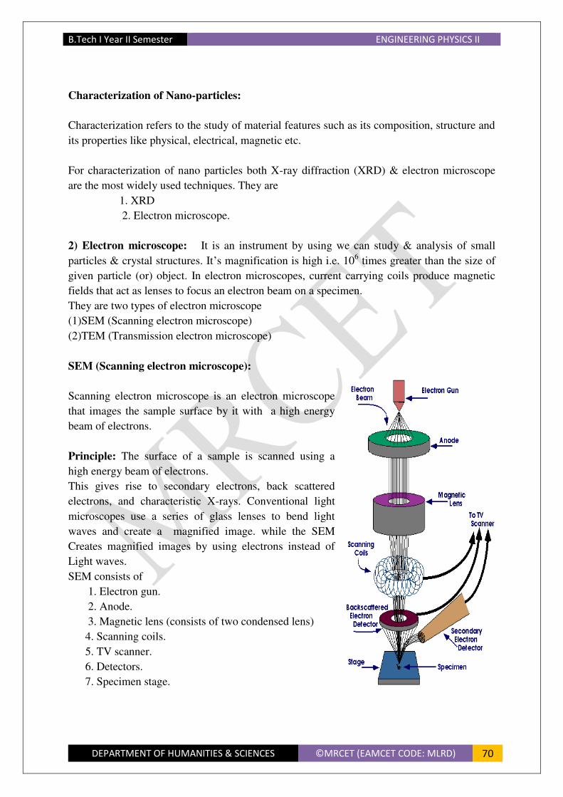
B.Tech I Year II Semester ENGINEERING PHYSICS II
DEPARTMENT OF HUMANITIES & SCIENCES ©MRCET (EAMCET CODE: MLRD) 70
Characterization of Nano-particles:
Characterization refers to the study of material features such as its composition, structure and
its properties like physical, electrical, magnetic etc.
For characterization of nano particles both X-ray diffraction (XRD) & electron microscope
are the most widely used techniques. They are
1. XRD
2. Electron microscope.
2) Electron microscope: It is an instrument by using we can study & analysis of small
particles & crystal structures. It’s magnification is high i.e. 106 times greater than the size of
given particle (or) object. In electron microscopes, current carrying coils produce magnetic
fields that act as lenses to focus an electron beam on a specimen.
They are two types of electron microscope
(1)SEM (Scanning electron microscope)
(2)TEM (Transmission electron microscope)
SEM (Scanning electron microscope):
Scanning electron microscope is an electron microscope
that images the sample surface by it with a high energy
beam of electrons.
Principle: The surface of a sample is scanned using a
high energy beam of electrons.
This gives rise to secondary electrons, back scattered
electrons, and characteristic X-rays. Conventional light
microscopes use a series of glass lenses to bend light
waves and create a magnified image. while the SEM
Creates magnified images by using electrons instead of
Light waves.
SEM consists of
1. Electron gun.
2. Anode.
3. Magnetic lens (consists of two condensed lens)
4. Scanning coils.
5. TV scanner.
6. Detectors.
7. Specimen stage.

B.Tech I Year II Semester ENGINEERING PHYSICS II
DEPARTMENT OF HUMANITIES & SCIENCES ©MRCET (EAMCET CODE: MLRD) 71
Construction and working:
1. The virtual source at the top represents the electron-gun which produces a stream of
high energy monochromatic electrons.
2. Electrons are attracted and travel through anode there by attains directionality.
3. Two magnetic lenses are used as condenser lenses to convert the diverging electron
beam into a fine pencil beam and condenser lens eliminated the high angled
electrons from the beam so electron –beam becomes thin and coherent.
4. A scanning coil is used to deflect the electron beam to scan the sample.
5. The objective lens is used to focus the scanning beam on a desired spot on the
sample.
6. When the high energy electron beam strikes the sample, some electrons scattered
due to elastic scattering (due to back scattering) called back scattered electrons,
some electrons are knocked off from the surface called secondary electrons and
some electrons penetrate deep into the inner shells of the sample atoms to knockoff
inner shell electrons due to which X-rays (wavelength matches)are produced.
7. The intensities of secondary electrons, back scattered electrons and X-rays recorded
using detectors and the signals are amplified and the images are then displayed on a
TV scanner (monitor).
8. This process is repeated several times.i.e.30 times/sec to get accurate results.
Applications:
1. Topography: To study the surface features of an object and its texture.
2. Morphology: To study the shape, size, arrangement of particles.
3. Composition: To study the elements and compound ratio in a sample.
4. Crystallography: Arrangement of atoms, and their order in the crystal.
5. SEM shows very detailed 3D images at much high magnifications as compared to
light microscopes.
6. The surface structure of polymer nano composites, fracture surfaces, nano fibres, nano
particles and nano coating can be imaged through SEM with great clarity.
TEM (Transmission electron microscope):
TEM is a powerful tool to investigate the lattice structure and defects on materials directly.
The first TEM invented by Ruska in April 1932 could hardly compete with optical
microscope with only 14.4 (3.6 × 4.8) magnification the basic components in TEM
are:
Electron gun
Condenser system
Objective lens (most important lens in TEM which determines the final resolution)
Diffraction lens
Projective lens (all lens are inside the equipment column, between apertures)
Image recording system (used to be negative films, now is CCD cameras)
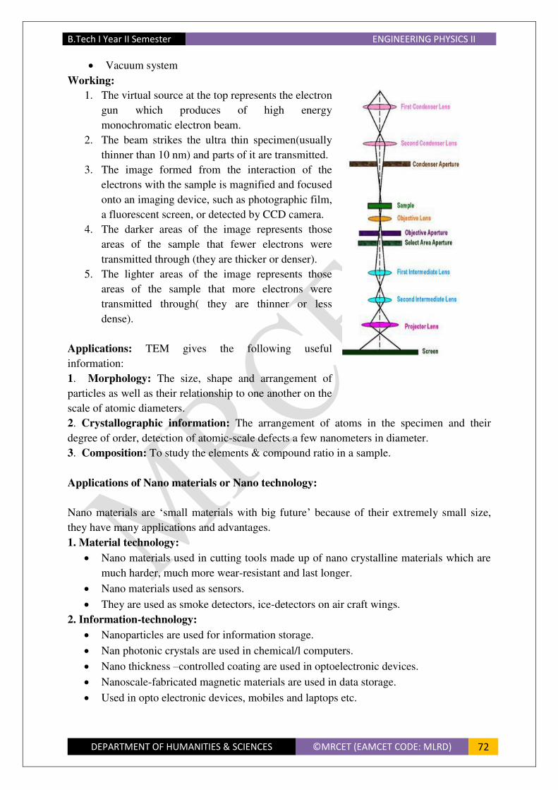
B.Tech I Year II Semester ENGINEERING PHYSICS II
DEPARTMENT OF HUMANITIES & SCIENCES ©MRCET (EAMCET CODE: MLRD) 72
Vacuum system
Working:
1. The virtual source at the top represents the electron
gun which produces of high energy
monochromatic electron beam.
2. The beam strikes the ultra thin specimen(usually
thinner than 10 nm) and parts of it are transmitted.
3. The image formed from the interaction of the
electrons with the sample is magnified and focused
onto an imaging device, such as photographic film,
a fluorescent screen, or detected by CCD camera.
4. The darker areas of the image represents those
areas of the sample that fewer electrons were
transmitted through (they are thicker or denser).
5. The lighter areas of the image represents those
areas of the sample that more electrons were
transmitted through( they are thinner or less
dense).
Applications: TEM gives the following useful
information:
1. Morphology: The size, shape and arrangement of
particles as well as their relationship to one another on the
scale of atomic diameters.
2. Crystallographic information: The arrangement of atoms in the specimen and their
degree of order, detection of atomic-scale defects a few nanometers in diameter.
3. Composition: To study the elements & compound ratio in a sample.
Applications of Nano materials or Nano technology:
Nano materials are ‘small materials with big future’ because of their extremely small size,
they have many applications and advantages.
1. Material technology:
Nano materials used in cutting tools made up of nano crystalline materials which are
much harder, much more wear-resistant and last longer.
Nano materials used as sensors.
They are used as smoke detectors, ice-detectors on air craft wings.
2. Information-technology:
Nanoparticles are used for information storage.
Nan photonic crystals are used in chemical/l computers.
Nano thickness –controlled coating are used in optoelectronic devices.
Nanoscale-fabricated magnetic materials are used in data storage.
Used in opto electronic devices, mobiles and laptops etc.

B.Tech I Year II Semester ENGINEERING PHYSICS II
DEPARTMENT OF HUMANITIES & SCIENCES ©MRCET (EAMCET CODE: MLRD) 73
3. Electronic industry:
Nano materials used in
Glass fibres.
Used to prepare laser diodes.
Optical switches
data memory
4. Medical field:
Nano materials used in drug delivery systems.
Used as agents in cancer therapy.
Used as active agents.
Used to reproduce or repair damaged tissues.