MAK302_04_p1.pdf
13
06.04.2014 dsdfsdf 1 MAK302-Elektronik MAK302 ELEKTRONİK Chapter 4 MAK302-Elektronik The BJT has three regions called the emitter, base, and collector. Between the regions are junctions as indicated. The term bipolar refers to the use of both holes and electrons as current carriers in the transistor structure BJT Structure B (base) C (collector) n p n Base-Collector junction Base-Emitter junction E (emitter) B C p n E p npn pnp The base is a thin lightly doped region compared to the heavily doped emitter and moderately doped collector regions.
-
Upload
kazim-basdemir -
Category
Documents
-
view
2 -
download
0
Transcript of MAK302_04_p1.pdf

06.04.2014
dsdfsdf 1
MAK302-Elektronik
MAK302
ELEKTRONİK
Chapter 4
MAK302-Elektronik
The BJT has three regions called the emitter, base, and collector.
Between the regions are junctions as indicated. The term bipolar
refers to the use of both holes and electrons as current carriers in
the transistor structure
BJT Structure
B
(base)
C (collector)
n
p
n
Base-Collector
junction
Base-Emitter
junction
E (emitter)
B
C
p
n
E
p
npn pnp
The base is a thin lightly doped region compared to the heavily doped
emitter and moderately doped collector regions.

06.04.2014
dsdfsdf 2
MAK302-Elektronik
In normal operation, the base-emitter is
forward-biased and the base-collector is
reverse-biased.
BJT Operation
npn
For the pnp type, the voltages
are reversed to maintain the
forward-reverse bias.
–
+ –
+
–
+
+
BC reverse-
biased
–
BE forward-
biased
–
+
+
–
–
BC reverse-
biased
+
BE forward-
biased
–
+
pnp
For the npn type shown, the collector is more
positive than the base, which is more positive than
the emitter.
MAK302-Elektronik
BJT Currents
IE IE
IC
IB
IC
IBn
p
n
p
n
p
+
– +
–
–+
IE
IC
IB
+
–
+
IE
IC
IB
+
–
–
npn pnp
The direction of conventional current is in the direction of the arrow
on the emitter terminal. The emitter current is the sum of the
collector current and the small base current. That is, IE = IC + IB.

06.04.2014
dsdfsdf 3
MAK302-Elektronik
BJT Characteristics
The collector characteristic curves show the relationship
of the three transistor currents.
The curve shown is for a fixed
based current. The first region is
the saturation region.
When both junctions are forward-
biased, the transistor is in the
saturation region of its operation.
Saturation is the state of a BJT
in which the collector
current has reached a maximum
and is independent of the base
current.
IC
B
C
A
0 0.7 V VCE(max)
VCE
Saturation
region
Active region
Breakdown
region
MAK302-Elektronik
BJT Characteristics
IC
B
C
A
0 0.7 V VCE(max)
VCE
Saturation
region
Active region
Breakdown
region
Once the basecollector junction is
reverse-biased, IC levels off and
remains essentially constant for a
given value of IB as VCE continues
to increase.
As VCE is increased, IC increases until B. Then it flattens in
region between points B and C, which is the active region.
For this portion of the characteristic
curve, the value of IC is determined
only by the relationship expressed
as
Ideally, when VCE exceeds 0.7 V, the base-collector junction becomes
reverse-biased and the transistor goes into the active, or linear, region
of its operation.
06.04.2014
dsdfsdf 4
MAK302-Elektronik
BJT Characteristics
IC
B
C
A
0 0.7 V VCE(max)
VCE
Saturation
region
Active region
Breakdown
region
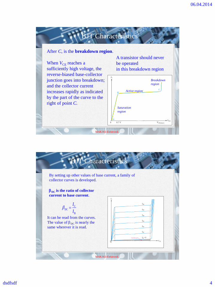
After C, is the breakdown region.
When VCE reaches a
sufficiently high voltage, the
reverse-biased base-collector
junction goes into breakdown;
and the collector current
increases rapidly as indicated
by the part of the curve to the
right of point C.
A transistor should never
be operated
in this breakdown region
MAK302-Elektronik
BJT Characteristics
0
IC
VCE
IB6
IB5
IB4
IB3
IB2
IB1
IB = 0Cutoff region
By setting up other values of base current, a family of
collector curves is developed.
bDC is the ratio of collector
current to base current.
It can be read from the curves.
The value of bDC is nearly the
same wherever it is read.
CDC
B
I
Ib

06.04.2014
dsdfsdf 5
MAK302-Elektronik
BJT Characteristics
What is the bDC for the transistor shown?
Choose a base current near the
center of the range – in this
case IB3 which is 30 mA.
IC
VCE
IB6
IB5
IB4
B3I
IB2
B1I
IB = 0
= 10 Am
= 20 Am
= 30 Am
= 0
= 60 Am
= 40 Am
= 50 Am
10.0
8.0
6.0
4.0
2.0
0
(mA)
Read the corresponding
collector current – in this case,
5.0 mA. Calculate the ratio:
CDC
B
5.0 mA
30 A
I
Ib
m 167
BJT Circuit Analysis
• When the base-emitter junction is forward-biased, it is like a forward-biased diode and has a nominal forward voltagedrop of.

06.04.2014
dsdfsdf 6

06.04.2014
dsdfsdf 7
MAK302-Elektronik
Cutoff
In a BJT, cutoff is the condition in which there is no base
current, which results in only an extremely small leakage
current (ICEO) in the collector circuit. For practical work, this
current is assumed to be zero.
IB = 0 –
+
–
+ICEO
RC
VCCVCE ≅VCC
RB
In cutoff, neither the base-emitter
junction, nor the base-collector
junction are forward-biased.
MAK302-Elektronik
Saturation
In a BJT, saturation is the condition in which there is
maximum collector current. The saturation current is
determined by the external circuit (VCC and RC in this case)
because the collector-emitter voltage is minimum (≈ 0.2 V)
In saturation, an
increase of base
current has no effect
on the collector
circuit and the
relation IC = bDCIB is
no longer valid. –
+ –
+
VCC
VBB
VCE = VCC – IC RC
RB
RC
IB
IC
–
+
– +

06.04.2014
dsdfsdf 8
MAK302-Elektronik
DC Load Line
the transistor. It is drawn by
connecting the saturation
and cutoff points.
The transistor
characteristic curves are
shown superimposed on
the load line. The region
between the saturation
and cutoff points is called
the active region.
The DC load line represents the circuit that is external to
0
IC
VCE
IB = 0 Cutoff
VCE(sat) VCC
IC(sat)
Saturation
MAK302-Elektronik
DC Load Line
What is the saturation current and
the cutoff voltage for the circuit?
Assume VCE = 0.2 V in saturation.
–
+ –
+VCC
15 V
VBB
3 V
RC
RB
βDC = 200
220 kW
3.3 kW
CCSAT
C
0.2 V 15 V 0.2 V
3.3 k
VI
R
W4.48 mA CO CCV V 15 V
Is the transistor saturated? B
3.0 V 0.7 V10.45 A
220 kI m
W
IC = b IB = 200 (10.45 mA) = 2.09 mA Since IC < ISAT, it is not saturated.

06.04.2014
dsdfsdf 9
MAK302-Elektronik
MAK302-Elektronik
06.04.2014
dsdfsdf 10
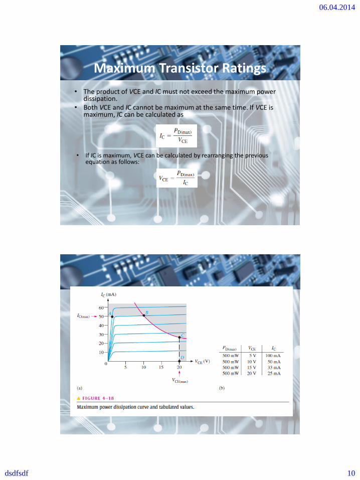
Maximum Transistor Ratings
• The product of VCE and IC must not exceed the maximum power dissipation.
• Both VCE and IC cannot be maximum at the same time. If VCE is maximum, IC can be calculated as
• If IC is maximum, VCE can be calculated by rearranging the previous equation as follows:

06.04.2014
dsdfsdf 11

06.04.2014
dsdfsdf 12
Power Derating
MAK302-Elektronik
Data Sheets
Data sheets give manufacturer’s specifications for maximum operating
conditions, thermal, and electrical characteristics. For example, an
electrical characteristic is bDC, which is given as hFE. The 2N3904 shows
a range of b’s on the data sheet from 100 to 300 for IC = 10 mA.
ON Characteristics
DC current gain ( IC = 0.1 mA dc, VCE = 1.0 V dc)
( IC = 1.0 mA dc, VCE = 1.0 V dc)
( IC = 10 mA dc, VCE = 1.0 V dc)
( IC = 50 mA dc, VCE = 1.0 V dc)
( IC = 100 mA dc, VCE = 1.0 V dc)
2N39032N3904
2N39032N3904
2N39032N3904
2N39032N3904
2N39032N3904
hFE2040
3570
50100
3060
1530
––
––
150300
––
––
–
Characteristic Symbol Max UnitMin

06.04.2014
dsdfsdf 13
MAK302-Elektronik
MAK302-Elektronik
End