
Majority logic circuits - Oregon State University
121
AN ABSTRACT OF THE THESIS OF SATISH KUMAR ANAND for the M. S. in Electrical Engineering (Name) (Degree) (Major) Date thesis is presented flay 7a 07-7, I9Gs- Title MAJORITY LOGIC CIR TS Abstract approved (Major pro essor This thesis considers the worst -case design of transistor circuits for the realization of Majority Logic. First the meaning of Majority Logic is discussed. The re- quirement of an odd number of inputs for the realization of Majority Logic is justified. The usefulness of Majority Logic in synthesizing a Boolean expression is shown with an example. Next, three separate circuits for the realization of Majority Logic are considered in detail. The three circuits are designated as: (1) Variable Threshold Transistor- Resistor Logic Circuit (VTTRL) (2) Variable Threshold Logic Circuit (VTL) (3) Transistor Tunnel -diode Resistor Logic Circuit (TTDRL). The three circuits are compared for their relative advantages and disadvantages.
Transcript of Majority logic circuits - Oregon State University

AN ABSTRACT OF THE THESIS OF
SATISH KUMAR ANAND for the M. S. in Electrical Engineering (Name) (Degree) (Major)
Date thesis is presented flay 7a 07-7, I9Gs- Title MAJORITY LOGIC CIR TS
Abstract approved (Major pro essor
This thesis considers the worst -case design of transistor
circuits for the realization of Majority Logic.
First the meaning of Majority Logic is discussed. The re-
quirement of an odd number of inputs for the realization of Majority
Logic is justified. The usefulness of Majority Logic in synthesizing
a Boolean expression is shown with an example.
Next, three separate circuits for the realization of Majority
Logic are considered in detail. The three circuits are designated
as:
(1) Variable Threshold Transistor- Resistor Logic
Circuit (VTTRL)
(2) Variable Threshold Logic Circuit (VTL)
(3) Transistor Tunnel -diode Resistor Logic Circuit
(TTDRL).
The three circuits are compared for their relative advantages
and disadvantages.

MAJORITY LOGIC CIRCUITS
by
SATISH KUMAR ANAND
A THESIS
submitted to
OREGON STATE UNIVERSITY
in partial fulfillment of the requirements for the
degree of
MASTER OF SCIENCE
June 1966

APPROVED:
rofessor of Elect fical "Engineering
In Charge of Major
ead of Department of `Electrical Engineering
Dean of Graduate School
Date thesis is presented /4-1el G17 )9G3"
Typed by Opal Grossnicklaus

ACKNOWLEDGMENT
The author would like to express his gratitude to
Professor Louis N. Stone, whose guidance and sugges-
tions added so much to the preparation of this thesis.
To Professor Donald Amort, the author expresses
his thanks for his useful suggestions.

TABLE OF CONTENTS
PART I MAJORITY LOGIC 1
PART II CIRCUIT #1 7
PART III CIRCUIT #2 48
PART IV CIRCUIT #3 70
PART V COMPARISON OF VTTRL, VTL, TTDRL CIRCUITS 92
BIBLIOGRAPHY 96
APPENDIX I 97
APPENDIX II 103
APPENDIX III 105

LIST OF FIGURES
Figure Page
1 Serial Binary Adder 5
2 "Majority -Logic circuit using VTTRL and Inverter circuit" 8
3 Base - emitter voltage when the transistor is OFF (assuming transistor to be open circuited) 11
4 Base - emitter diode characteristics 11
5 Effect of Leakage- current 16
6 -A Worst -case OFF condition (VTTRL) 19
6 -B Worst -case ON condition (VTTRL) 19
7 -A Output voltage tolerance 26
7 -B Base - emitter junction voltage tolerance 26
8 Maximum base -ON current 28
9 Minimum available turn -OFF current 28
10 -A Inverter circuit 31
10 -B Worst -case ON condition (Inverter) 31
10 -C Worst -case OFF condition (Inverter) 32
11 Theoretical wave shape prediction 37
12 Observed response (one DC; one pulse input) 39
13 Wave shapes for one D -C; one pulse input 40
14 One input D -C, two pulse inputs 41
15 One D -C input, two pulse inputs 42
16 Transient response improvement using speed -up capacitors (INVT) 47

Figure
LIST OF FIGURES (Cont'd)
Page
17 Variable threshold logic circuit 47
18 -A Worst -case OFF condition 53
18 -B Worst -case ON condition 53
19 Tolerance of RT and Ro 57
20 Maximum base ON current 61
21 Minimum available Turn -OFF current 61
22 VTL circuit wave shapes 66
23 VTL. One D. C. input, two pulse inputs 67
24 Base voltage variations 68
24 A, Tunnel -diode characteristics (with 100 ohms parallel B, C, D resistor 71
24 F, G Tunnel -diode characteristics (with 60 ohms parallel - resistor 73
25 Transistor tunnel -diode circuit 80
26 -A Worst -case OFF conditions 82
26 -B Worst -case ON conditions 82
27(A) Maximum base ON current 87
27(B) 87
27(C) Minimum available turn -OFF current 87
28 -A TTDRL circuit (one D. C. , one pulse) 90
28 -B One D. C. , two pulse inputs 91
29 Plot for finding KC of the rise time equation 99

LIST OF FIGURES (Cont'd)
Figure Page
30 Plot for finding KC of the fall time equation 100
31 Plot for finding KC of the storage equation circuit 1
Function KC 102

LIST OF TABLES
Table Page
I Threshold and its complementary level 2
II Three -input majority -logic truth table 3
III 2N 1305 PNP(Ge) transistor characteristics 17
IV Pre -assigned parameters 18
V Tolerance effect 24
VI Switching times 44
VII A 2N 2713 NPN silicon epitaxial transistor characteristics 51
VII -B Pre -assigned parameters 52
VIII R,I, v/s Ro 58
IX Circuit parameter tolerances 59
X Comparison of switching times 65
XI(A) 2N 967 PNP Ge transistor 77
XI(B) Preassigned parameters 78
XII Effect of parallel- resistor, parameter tolerances on the working of the TTDRL circuit (I
c = 1 5mA) 84
XIII Comparison of switching times 89
XIV Transistor switching times 104

SYMBOLS
K1 (1 +x) Upper limit resistance tolerance
K1(1 -x) Lower limit resistance tolerance
N # of fan -out
M # of fan -in
L Threshold value in units of fan -in
(V )''` cs Maximum collector ON voltage at (Ib ) ,
1
(Vcs),;, Minimum collector ON voltage
Vbsl Maximum base ON voltage at (Ib 1
(V ).. bo
Minimum base OFF voltage (if base -emitter diode is
reverse biased)
(V )* Maximum base OFF voltage (if base -emitter diode is
forward biased)
(Ic') Maximum collector current at (Ib )
1
(Ibs) Worst case base current at edge of saturation for Ic'
(hfe),,, Minimum forward current transfer ratio
(I ')
(h ):;. = c
(hfe)'' (Ibs) ,,
(Ib ).;<
1
Minimum base ON current
CS
s
) )0
e

(I o
I co
(I )' rc
v c
SYMBOLS (Cont'd)
Minimum overdrive factors (Ib )` /(Ibs)`
1
Maximum base OFF current (if base - emitter diode is
reverse biased)
Minimum base OFF current (if base -emitter diode is
forward biased)
Maximum collector OFF current at maximum operating
temperature
Maximum reverse clamping diode current
Forward voltage drop of clamping diode
Minimum value
Maximum value
Normal Beta (Forward current transfer ratio)
Pc Turn ON circuit beta ((Ic') )''`)
max 1
ßcc Turn OFF circuit beta (Ic' /(I 2') *) =
P c Turn ON circuit (storage) beta (Ic' /(Ib ) *)
min m
(I0)*
( )o
( )O
pl' pT hfe

MAJORITY LOGIC CIRCUITS
PART I
MAJORITY LOGIC
Majority logic can be represented in the form of a Boolean
expression as
M = A B + B C + C A (1)
it the three inputs are A, B, and C. In other words, the form of
the output depends on the majority of the inputs. There is a con-
cept of practical value which is useful in the design of the majority
logic. It appears here as LC, the complementary threshold level.
Given a function, its complement is the funtion which results when
the logical states, input and output, are inverted. The complemen-
tary level is found from the equation (2).
LC =M -L +1 (2)
where M = total number of inputs
L = threshold level
LC = complementary threshold level.
In the case the Majority Logic
LC = L (6). (3)
This limits the use of majority -gates with an odd number of inputs
(table I).

2
Table I. Threshold and its complementary level
Number M L LC Is L= LC ?
1 2 1 2 No
2 3 2 2 Yes
3 4 3 2 No
4 5 3 3 Yes
5 6 4 3 No
6 7 4 4 Yes
In table I, it is noted that for all odd number of inputs, L =Lc;
while for even number of inputs, L # L. The importance of L # L is realized when a function F has
to be synthesized using only majority gates.
According to Lemma I (1, p. 15), if F is synthesized using
only majority gates, then for any input a .,
F(a .) = "not" F( "not" a .) . (4)
This says that if F is built with only majority gates, then
complementing the inputs to F will result in the outputs being
complemented. This condition can be satisfied only if, L = L. Hence it follows that a majority gate must have an odd num-
ber of inputs.
The truth table representation of the three -input Majority -
Logic is as shown in the table II.

3
Table II. Three -input majority -logic truth table
A B C M
o o o o
o o 1 o
o 1 o o
o 1 1 1
1 o o o
1 o 1 1
1 1 o 1
1 1 1 1
Usefulness of Majority Logic
As shown in equation (1), the Boolean representation of three -
input Majority Logic is,
M= AB +BC +CA (5)
if a Boolean function of this kind is to be realized using AND -OR
Logic, it requires three AND gates and one OR gate. The same
function can be realized by using one Majority gate. This does not
necessarily mean that there will be a reduction in cost and corn-
ponents. It will depend on the type of Majority circuit designed, and
the type of components used in its design.
A simple example (4, p. 23 -24) of synthesizing a serial- binary

4
adder using conventional AND -OR- Invert logic and Majority- Invert
Logic is considered. Fig. 1 -A shows the synthesized serial binary
adder using AND -OR- Invert logic. It uses four AND gates, four OR
gates and one Invert gate, making a total of nine gates with 17 input
elements. It is possible to realize this circuit in other ways but this
is one of the simplest, unless special rather than general gates are
used.
Fig. 1 -B shows the same adder using Majority- Invert gates.
This arrangement requires three Majority and one Invert gate, mak-
ing a total of four gates with ten input elements.
The preceding example does not prove that a digital machine
composed of three -input M gates and INVERT gates will require
less than 50 percent of the circuits required for the more conven-
tional gates. It merely illustrates that M gate approach is simpler
in certain cases.
Another important use of Majority Logic comes in the design
of Reliable circuits (5, p. 43) using Majority Redundancy techniques.
In order to have a reliable binary operation, an odd number of
identical binary units are used in parallel with their inputs connected
together and the outputs fed into a Majority gate. If the number of
binary units connected is three, one of the units can fail while the
redundant system still functions properly.
The importance of Majority Logic in the design of reliable

DANDGate [9_ OR Gate
C. i
(A)
(B)
Fig. 1. Serial Binary Adder.
Inverter
R. i
- AND e i
2

6
machines and in synthesizing complex Boolean functions, thus, can
not be overlooked.
The problem now is to design a Majority -Logic Circuit, which,
in itself is simple, at least as fast as the conventional logic circuits
and not very expensive.
Three different circuits are considered in detail and then com-
pared for relative advantages and disadvantages.

7
PART II
CIRCUIT # 1
Variable Threshold Transistor Resistor Logic ( VTTRL)( 6)
The VTTRL circuit considered here uses transistor in corn-
mon-emitter configuration (Fig. 2). This results in the inversion
of the output. Hence an additional transistor is used to get the
output in the true form.
The design of the Majority -Logic circuit is divided into two
parts: (1) Design of VTTRL circuit: Here the transfer -resistors
(RT) are used to act as a Kirchoff's -Adder for current, such that
the transistor turns ON when the Majority of the inputs are present
(equal to -EC volts). The number of inputs in this design is three.
(2) Design of Inverter circuit: This design is similar to an ordinary
NOR circuit design, where there is only one input. The transistor
turn ON, when the input ( -E volts) is present.
Effect of Source Impedance (RS)
Ideally a voltage source should have zero impedance. In
practice, the impedance of the voltage source should be negligible
as compared to the load (transfer- resistors in this case).
C

M
L
RT
+E2 o -El o
al Dl
+E 2
RT a2
RT a3
RT' T
b 1
C i----
T b2 1 RT' T - b
n
VTTRL RT - Transfer -resistor for VTTRL
RT' - Input Resistor for Inverter stage D - Clamping Diode
M - Number of inputs L - Threshold level N - Fan -out
RS - Source impedance of inputs
-E '
1
Inverter
Fig. 2. "Majority -Logic circuit using VTTRL and Inverter circuit ".
00
R2 R1
o
-
a4 RT
\ .-- a 5
RT
-An/.--y an

9
Due to the clamping of the output in each VTTRL and inverter
stage, the source impedance of an OFF transistor will be very small
(equal to the forward -resistance of the clamping diode).
Also assuming that the flip -flops which supply the voltage pulse
to the first stage of the VTTRL circuit have diode - clamping, their
source impedance can be neglected.
The source impedance of the D -C voltage supply is about lohm to
2 ohms, and if transfer - resistors are of the order of a few k -ohms,
it will be less than O. 5% of the transfer- resistors.
If however the transfer -resistors are assumed to be ±1% tol-
erance, and the source impedance is about 50 ohms, it has to be
taken care of. This can be done by selecting the transfer -resistors
50 -ohms less than the calculated value.
The Majority Logic circuit of Fig. 2. operates as follows:
(1) VTTRL: When one of the three inputs is -(EC) volts and
the other two are zero, representing logic 1 and logic 0 respec-
tively, the base - emitter voltage of the transistor is made slightly
positive by the use of +E2, R2 current source. At this time, the
transistor is cut -off and the collector voltage is equal to ( -EC)
volts. The use of the clamping Diode D is to reduce the voltage
swing from ( -El) to ( -E) volts. This results in a smaller value
for the transfer resistors (RT), which helps improve the transient
response of the circuit.

10
When two of the inputs are ( -EC) volts and one is zero volts,
the current supplied by the transfer resistor not only nullifies the
effect of back biasing current source (E2 -R2) but also supplies
enough current to the base -emitter junction of the transistor to
saturate the transistor, and thus make the collector voltage zero
volts,
The circuit operation is such that when one of the inputs is
1 ( -EC volts) and the other two are 0 (O volts), the output is 1( -EC
volts). When two or more of the three inputs are 1( -EC volts) the
output is 0 (0 volts). Thus the output wave form is inverted. Hence
an additional inverter stage is required to obtain the output in the
desired form. The base - emitter voltage is determined by the mag-
nitude and the direction of the current flowing in the base - emitter
junction.
When the transistor is to be kept OFF, a small reverse cur-
rent is allowed to flow through the base - emitter junction to take
care of the leakage collector current. Under these circumstances,
the transistor is an open circuit for all practical purposes. The
steady state base voltage will then be determined by current sup-
plied by the reverse biasing current source (E2 /R2) and the Input
current (Fig. 3).
In the present case, assuming V n
is the base emitter voltage,

V cs RT/2
11
E O n, Vn O e c RT
ob
Fig. 3. Base - emitter voltage when the transistor is OFF (assuming transistor to be open circuited).
Vbe
O
l Ib
Fig. 4. Base - emitter diode characteristics.
4--
+E2

12
E Vn
=(Io) + EcR Vn +
(V
T/2
Vn)
2 I' (6)
Vn will vary according to the variation of E2, R2, Ec and RT. In
order to keep the transistor OFF under worst -case conditions, V n
should be slightly positive for a PNP transistor. Some designers
assume this minimum voltage to be 0. 5 v, and some 0. 1 v ( 2).
Base- Emitter junction voltage when the transistor is ON
The base - emitter diode is clamped to a certain negative voltage.
Once this voltage is reached the base- emitter junction is forward bi-
ased. Its characteristics are as shown in Fig. 4. This character-
istic has a certain tolerance. Hence for a particular base current,
Vbe has a minimum and maximum limit.
Also as the current through the base -emitter junction increases
the base- emitter junction voltage increases according to the char-
acteristics.
Hence, when the transistor is saturated, there has to be an
equilibrium among the various current sources and the base - emitter
junction diode.
VTTRL Design
Design objective: The basic goal of the design is to insure an
-
R +
+
RT,

13
adequate separation between the OFF and ON values of the threshold
function in the worst -case situation so that in all other situations,
there will be no possibility of losing distinction between the two
states. This is done for the OFF state by specifying the minimum
OFF base voltage (Vbo).;,, and for the ON state by specifying the
minimum ON base current (Ib 1
The design carried out here is based on Worst -case calcula-
tions. This approach is preferred over other methods, such as,
Statistical Design because,
1. This design is more reliable.
2. The calculations are much simpler.
3. In the design of VTTRL circuit the tolerance limits on
components cannot be appreciably increased by the use of Statistical -
Design.
Important Parameters
(Vbo):;: bo Minimum Base OFF Voltage
In order to keep the transistor OFF in the presence of maxi-
mum leakage current the base - emitter junction is reverse biased.
Under the Worst -case conditions, this voltage is assumed to be
+(0. 1) volts for the PNP transistor used in this circuit.
);.

14
(Vcs)* Maximum Collector ON Voltage
Ideally, the collector ON voltage should be zero volts. If it
is not zero volts, it has to be considered with respect to the next
stage, because it will supply a small current to the base of the next
transistor stage. It depends on the transistor parameters. Hence
a transistor with a low (Vcs)* < is preferable. cs
(Ic') Maximum Collector Current at (Ib ) ,,
The maximum collector current can be arbitrarily chosen for
a particular transistor depending on the collector voltage E1 and
the collector resistance R1. Its maximum value is however lim-
ited by the maximum power dissipation permissible for the transis-
tor being used.
(hfe),,, Minimum Forward Current Transfer Ratio
(hfe);,, is the most important parameter in the design of VTTRL
circuits. It determines the minimum Worst -case base current re-
quired to just saturate the transistor. The transistors used for the
VTTRL circuit should not have their (hfe) minimum below (h
the circuit will not function. otherwise

15
(I )* co
Maximum Transistor Leakage Current
The transistor leakage current, though very small at 25°C,
doubles for every 10°C rise in temperature. Hence if the designed
circuit has to operate at 70°C, the leakage current at 70°C should
be considered in the design. The best way to reduce its effect is to
pass a current equal to (Io) in the base of the transistor in the oppo-
site direction. This will cancel Pao)* in the collector. Thus the
leakage current is reduced from (l +ß)(I0)* to (I0)* (Fig. 5).
Selection of a Transistor for VTTRL Circuit
The most important parameter in the steady- state, worst -case
design of VTTRL is the minimum forward current transfer ratio,
or (hfe) '
In order to have a design useful for all transistors of a
particular type, it is necessary to know (hfe) minimum for this
transistor. Also for a particular transistor, (hfe) minimum should
not drop below the specified (hfe),;., throughout the working life of
the transistor.
The speed of the switching circuit will be determined by the
type of transistor, i. e. , its Turn -ON and Turn -OFF times, a - cutoff
frequency etc. The transient -response for VTTRL is similar (6 )
to TRL circuits.
The transistor chosen for the design of the following VTTRL

16
(A) Transistor in Active Region
(B) Transistor in OFF Region
Fig. 5. Effect of Leakage - current.
17
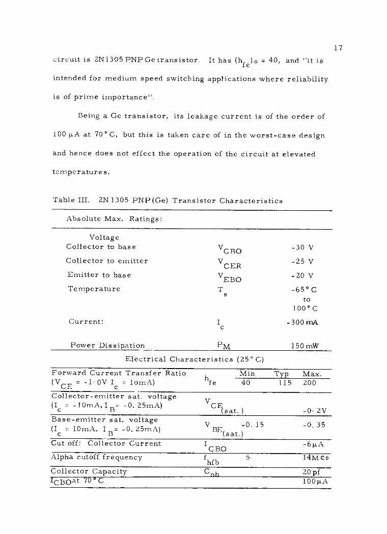
circuit is 2N1305 PNP Ge transistor. It has (hfe),;; = 40, and "it is
intended for medium speed switching applications where reliability
is of prime importance ".
Being a Ge transistor, its leakage current is of the order of
100 µA at 70°C, but this is taken care of in the worst -case design
and hence does not effect the operation of the circuit at elevated
temperatures.
Table III. 2N 1305 PNP(Ge) Transistor Characteristics
Absolute Max. Ratings:
Voltage Collector to base VCBO -30 V
Collector to emitter VCER -25 V
Emitter to base VEBO -20 V
Temperature Ts -65°C to
100 ° C
Current: I c
-300 mA
Power Dissipation PM 150 mW
Electrical Characteristics (25°C) Forward Current Transfer Ratio Min Typ Max. (VCE = -1.0V lc = lomA) hfe 40 115 200
Collector- emitter sat. voltage (Ic = - l OmA, I B= -0. 25mA) VCE (sat. ) -0. 2V Base-emitter sat. voltage (Ic = 10mA, IB= -0. 25mA) VBE
-0.15 -0. 35
Cut off: Collector Current I -6µA Alpha cutoff frequency fhfb 5 14Mcs
Collector Capacity Cnh 20 pf ICBOat 70°C 100µA

18
Table IV. Pre- Assigned Parameters
(1+x) 1.03
K1 (i-x) 0.97
M 3
L
( V )''` cs
2
-0. 20V
-0. 35V
+0. 10V
I' lOmA c
(Ibs)';. 10/40 = 0. 25mA
(hfe)''` 40
(p).;. (lb ).;:/(Ibs)* 1. 20 1
) 0. 30mA 1
(I)* 0. 12mA o
(V)''` 0. 01 V cs (I ) ;< 0. 05mA rc
v 0.1V c
0 O. 45V Vbs(3)
E -15V 1
E 2 +15V
E -5V c
K1
(Vbs )'` 1
(
(Ib

(R
(E )+v (R
C.)
19
Fig. 6-A Worst-case OFF condition (VTTRL).
Fig. 6-B Worst-case ON condition (VTTRL).
cs e
-(E
-(V )'
- c N\/\,-
20
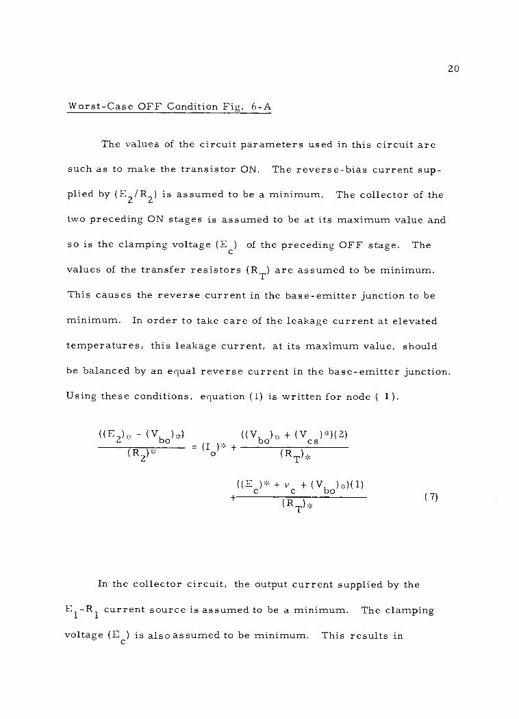
Worst -Case OFF Condition Fig. 6 -A
The values of the circuit parameters used in this circuit are
such as to make the transistor ON. The reverse -bias current sup-
plied by (E2 /R2) is assumed to be a minimum. The collector of the
two preceding ON stages is assumed to be at its maximum value and
so is the clamping voltage (E ) c
of the preceding OFF stage. The
values of the transfer resistors (RT) are assumed to be minimum.
This causes the reverse current in the base - emitter junction to be
minimum. In order to take care of the leakage current at elevated
temperatures, this leakage current, at its maximum value, should
be balanced by an equal reverse current in the base -emitter junction.
Using these conditions, equation (1) is written for node ( 1).
((E2),. - ( Vbo).;.) ((Vbo):;: + ( Vcs) '`)( 2)
(R2)* - (Io)' + (RT),
+((Ec) ` + vc + (Vbo)''`)(1)
(RT).,
In the collector circuit, the output current supplied by the
E1 -R1 current source is assumed to be a minimum. The clamping
voltage (E )
c is also assumed to be minimum. This results in
( 7)

21
minimum current supplied to the output transfer resistors. The
output of the VTTRL is connected directly to an Inverter circuit;
the base -ON voltage of Inverter circuit is assumed to be the maxi-
mum for this condition. If the transfer resistors at these conditions
are at their minimum value, the number of outputs is reduced to a
minimum. It is also assumed that a leakage current (I )* is flow - co ing in the collector at this time, which is also obtained from (E1, R1),
thus reducing the current supplied by (E1, R1) to the output transfer
resistors to a minimum. Writing the current equations for Node (2),
( Vbs ,)*) X N ((E1)- - (Ec);;.) ((Ec)>;. - 1
(R1)' 'co () + (RT)*
Worst -Case ON Conditions Fig. 6 -B
(8)
In the collector circuit, the current supplied by the (E1R1)
current source and the reverse current through the clamping diode
balance the maximum collector ON current and the small current
taken by the succeeding Inverter stages which is assumed to be OFF.
As the maximum collector ON Current is assumed to be of a fixed
value, the increase in fan -out will decrease this current. Decrease
in the collector current results in reduced base ON current, which
if it becomes appreciably less, will turn ON the transistor when it
should not. This also limits the maximum number of outputs
22
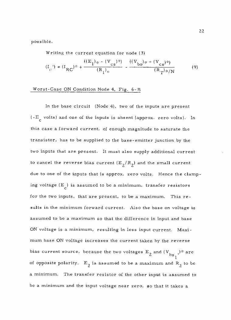
possible.
Writing the current equation for node (3)
((El)* - (Vcs) *) ((Vbo) ;< + (Vcs)) (I') = (I RC)* + - (9) c RC (RI)* (RT) */N
Worst -Case ON Condition Node 4, Fig. 6 -B
In the base circuit (Node 4), two of the inputs are present
( -E c
volts) and one of the inputs is absent (approx. zero volts). In
this case a forward current, of enough magnitude to saturate the
transistor, has to be supplied to the base - emitter junction by the
two inputs that are present. It must also supply additional current
to cancel the reverse bias current (E2 /R2) and the small current
due to one of the inputs that is approx. zero volts. Hence the clamp-
ing voltage (E )
c is assumed to be a minimum, transfer resistors
for the two inputs, that are present, to be a maximum. This re-
sults in the minimum forward current. Also the base on voltage is
assumed to be a maximum so that the difference in input and base
ON voltage is a minimum, resulting in less input current. Maxi-
mum base ON voltage increases the current taken by the reverse
bias current source, because the two voltages E2 and (Vbs 1) are 1
of opposite polarity. E2 is assumed to be a maximum and R2 to be
a minimum. The transfer resistor of the other input is assumed to
be a minimum and the input voltage near zero, so that it takes a

maximum current.
The Node equation is:
((Ec),;: (Vbs 1
')''') X 2
= (Ib1)* + (R2),;,
((E2)* + (Vbs ')`)
((\T bs ')
* - (Vcs) ,,)( 1)
1
(R ,I,) ,,
Calculation of Circuit Parameters
(10)
23
All the calculations done here are for
M = 3, L = 2.
Four equations (equations 7, 8, 9, 10) are written for as many un-
knowns. The unknowns are RT, R1, R2, N.
It is possible to assume clamping voltage ( -E ) c
as unknown,
and then solve the four equations to get N = f(RT), and maximize, N.
After going through one such calculation, it was found that N max lies between 4 and 5. E
c for this case is slightly higher than 5 volts.
The solution for N = f(RT) results in a fourth degree equation and
the calculations are very involved. On assuming E c
= -5 volts and
then solving the four equations (7, 8, 9, 10) for the four unknowns
gives Nmax 4. In this case the solution N = f(RT) is in the form
of a second degree equation, and is much simpler.
The calculation here are based on the assumption that the
-
(RT)"
=

24
succeeding stage is an inverter circuit, i. e. , when VTTRL is OFF,
Inverter is ON and vice -versa. It is possible to use the fan -out
directly as the fan -in of a VTTRL circuit. Due to change in base -
voltage conditions (it may be OFF or ON depending on majority of
the inputs), the fan -out is reduced to 3. The fan -in for the Inverter
is 1, so that the speed -up capacitor can be used without causing
"Cross -talk, " which occurs, if the fan -in is more than 1, due to the
interaction between various inputs.
Effect of Tolerance on the Design of VTTRL Circuit
Due to the use of threshold of inputs in VTTRL, the usual
tolerance limits (used in TRL NOR Logic) can not be used.
On increasing the tolerance limits for voltage supplies and
resistors, the value of transfer resistor starts decreasing, after a
certain limit, the value of RT becomes negative, i. e. , the design
is not feasible.
Table V shows the effect of tolerance limits on RT.
Table V. Tolerance effect
No. Voltage supply Resistor Value of tolerance limit tolerance limit R in KO
1 3% 3% 2.90 K 2 3% 5% 1.62 K 3 5% 5% 0.044 K 4 10% 10% -10.4 K

It was therefore decided to use 3% tolerance limit for resistors
and voltage supplies.
Values of the unknowns:
R,I, = 2. 90 ± 3 %KS2
R2 = 6. 25 ± 3 %KS2
N = 4. 04 max
R1 = 1. 54 ± 3% KS-2
Though most of the resistors available commercially are
25
of 5%
or 1% tolerance, it is usually stated that the 1% resistors vary to
3% tolerance limit in their working life.
Also, the purpose of the design, here is to show how much
maximum tolerance limits can be imposed on the components.
For this design, the output voltage tolerance and base - emitter
junction voltage tolerance will be as shown in Fig. 7 -A and 7 -B.
Maximum Power Dissipation for Each Variable Threshold TRL Circuit ( 6 )
(E22)'' (E12)^`
(Ec2)) N(R
(11)
(12)
Pmax(ON)
Pmax(OFF)
(R2).;.
(E22)''`
+ (R1)-,=
(E1)* ((El),,,
- (R2)* + (R 1) ''`
(Ec) '`) - T
).;.
Pmax(ON) = 196. 8 mW
max(OFF)= 86.45 mW P
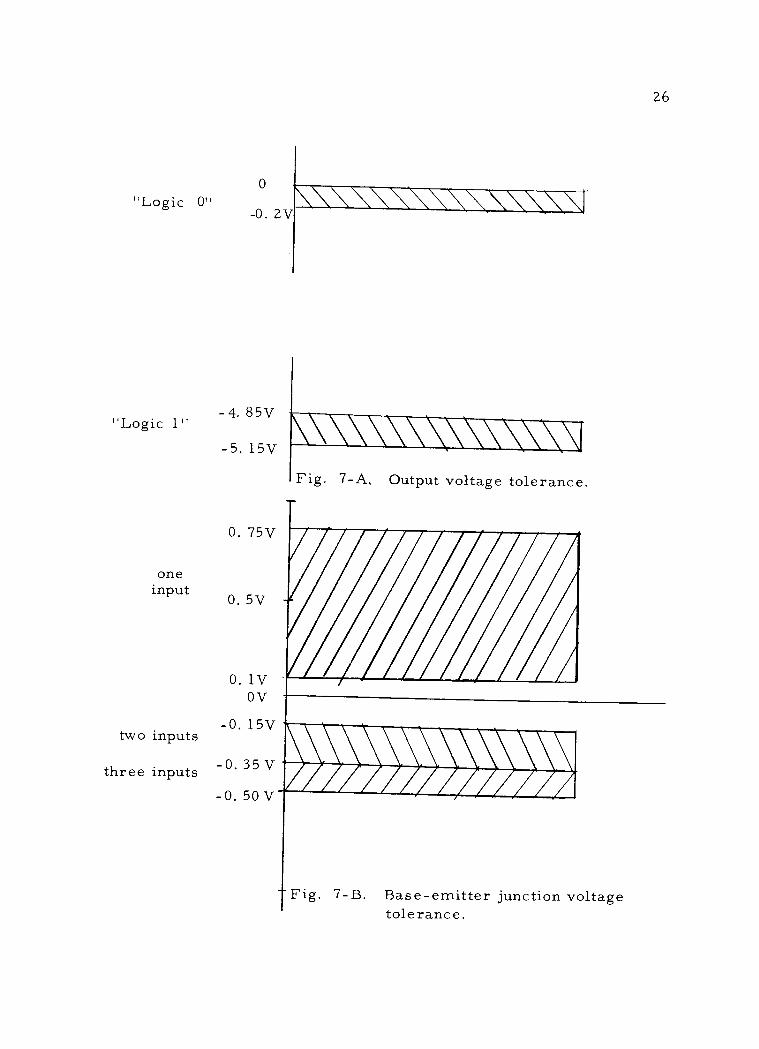
"Logic 0"
"Logic 1"
one input
two inputs
three inputs
0
26
-0. 2V
-4. 85V
- 5. 15V
0. 75V
0. 5V
O. 1V OV
-0. 15V
-0. 35 V
-0.50V
====1 Fig. 7 -A, Output voltage tolerance.
Fig. 7 -B. Base - emitter junction voltage tolerance.
Ar

27
For 50% (Worst case) duty cycle
PAV = 141. 63 mW
p max = 150 mW
(allowed)
Hence the operation is well within the dissipation limits.
Transient Response
In order to calculate the transient response, some additional
parameters have to be determined.
(1) (Ibm)'` = Maximum base ON current (Fig. 8).
M((Vco) - Vbs'(3)) ((E2)>; + Vbs(3)) (Ibm).,, - (RT)* (R2)>,,
(Vco)* = Maximum collector OFF voltage
(13)
Vbs'(3) = base ON voltage when all the three inputs are
present. It is assumed to be slightly higher then,
(Vbs ')* = Max base ON voltage at (Ib ).;<.
1 1
(Ibm),,, obtained here was equal to 2. 68 mA.
(2) (I2') = Minimum available transient turn OFF current.
The current (I2') is chosen as the Worst -case turn OFF,
immediately following (Ibm) i. e. , the ratio (Ibm)*/(I2')* is
maximum. For this case base voltage = V bs ' (3)' The tolerance of
the (RT,)* resistors was established for (Ibm and it is not m

28
Fig. 8. Maximum base -ON current.
Fig. 9. Minimum available turn -OFF current.

29
reasonable to assume that some (M -L +1) would change to the upper
bound, just as the transistor is switched OFF. Hence (I2'),., is
designated as the minimum available turn OFF current. The true
steady state (I2),; as calculated in Worst Case OFF condition for
base voltage (Vbo).;, is not used for transient conditions.
((E2),. + Vbs'(3)) ((Vbs(3) )
- (Vcs)*)(M-L+1) (I2')>,
((Vco)* (Vbs,(3)))(L -1)
(I2') . = 0. 82, (Ibm) * /(I7')>.. = 2. 68/0. 82 = 3. 27
(14)
Worst -case transient response prediction for 2N1305 tran-
sistors with t total (max) = 1. 50 µ sec. (For VTTRL)
Though the minimum a cutoff frequency for ?N 1305 is 5Mc /s
and typical a - cutoff frequency is 14 Mc is (Appendix I), it was found
that the majority of the transistors tested in the lab had their turn
ON and turn OFF time very close to the times for a typical transistor
as given in the data sheet.
On this basis, the Worst case transient response was calcu-
lated (Appendix II) for the variable threshold logic and its typical
collector and base currents.
- (R2'),, + (RT).
(RT) -

30
td+ tr = 0. 90 p.sec. max.
tf = 0. 38 p.sec. max.
t s
= 1. 11 p.sec. max.
The observed max. times are: (Fig. 12, 13)
td + tr = 0. 60 ..sec. (two inputs)
tf = 0. 40 p.sec. (two inputs)
t s
= 0. 60 p.sec. (three inputs)
The difference in the observed and calculated values is because of
the fact that the worst case max. base ON current (Ibm)* is not
reached resulting in less storage time.
The turn -on time (0. 60 p.sec. ) is less than the worst -case
calculated turn -on time (0. 90 µsec.) because under worst -case a
base current of 0. 30mA is required to just turn -on the transistor,
but under normal circumstances this current is much higher. In
this circuit it was found to be 0, 50 mA. This changes the circuit
ß from 33. 3 to 20 which results in the reduction of calculated rise -
time from 0. 90 to 0. 54 µs. Adding a delay time of 0. 06 µs, the total
turn -on time is now 0. 60 µs.
Fall time seems to agree for both the observed and calculated
cases. This is because the turn -off currents in the two cases are
approximately equal.
Hence it can be concluded that when the worst -case design is
used for calculating the steady -state and transient response, the

31
Fig. 10A. Inverter circuit.
Fig. 10 -B. Worst -case ON condition (Inverter).
+(E 2)*

32
c)-(Vcs)*
Fig. 10-C. Worst-case OFF condition (Inverter).
0 W.. -(V cs ' (R +(V
T bo
+(E
R
c)j(I )* 0

33
switching times calculated for the worst case conditions are much
longer than the observed times (under typical conditions).
For the standard TRL Inverter circuit, the fan -in is just one.
The fan -out is to be maximized.
Under the Worst -case OFF condition (Fig. 10 -C), the preced-
ing transistor is assumed to be ON. Similar to the case of VTTRL
worst -case design, the parameter values are assumed, such that
the reverse bias current due to (E2, R2) is a minimum, and the
current due to the preceding ON stage is a maximum. The reverse
base - emitter bias current is the difference of these two currents
and is therefore a minimum.
In the collector circuit, the fan -out can be connected to both,
ON and OFF transistors. In the worst case it is assumed, that one
of the outputs is connected to an ON transistor, and the rest of the
outputs are inputs for transistors which are OFF.
The fan -out connected as fan -in for an ON transistor will have
its transfer resistor (RT) at its upper tolerance limit. The fan -out
connected as fan -in for OFF transistors will have their transfer
resistor at its minimum tolerance limit.
The four node equations are then written, as in case of VTTRL.
Equations (15) for Node (1) in Fig. 10 -C and Equation (16) for Node
(3) in Fig. (10 -B) are solved for (R2) and (R2) . Equation min max
(1 7) for Node (2) in Fig. 10 -B and Equation (18) for Node (4) in

Fig. 10 -C are solved for N and R1.
Node (1) Worst -case OFF
E2)* - (Vbo) *) ((Vcs)'' + (Vbo):)
(R2) ' (Io)' + (RT)*
34
(15)
In this equation all the parameters are known except (R2) *. Hence
(RL)* is determined using equation (1).
Node (3) Worst -case ON
((E - (Vbs )'`) ((E 2)* + (Vbs i)*)
c
,
1 - (I )''` + b (R ): (R )' 1
T 1 2
From this equation (R2)* is calculated.
(R2)* = (R2) max.
= 64k
(R2)* _ (R2) = 14. 5k min
Choosing a value near (R2) max
(16)
increases the base current result-
ing in a larger storage time. Hence R2 is chosen close to (R2) min
R2 = 15 k
Additional base current for fast rise is provided by the speed up
capacitor.
_
,
,

35
Worst -case ON: Node (2)
( Ic) = ((E1),, - (Vcs)`) ((Vbs)(M
-L)'' -(Vcs),) (IRC) (R1)* (RT),:, /N
Worst -case OFF: Node (4)
((El).;. - (Ec)>:) ((Ec). :. + (Vbo))(N -1)
(R1)' = (Ico) + (RT)..
((EC),:, - (Vbs' 1
)''`)
+ (RT)*
(1 7)
(18)
Using equations (2) and (4), the two unknowns N and R1 are calcu-
lated.
For
N = 3.
N = 3.
60
0
R 1
= 1. 52 k.
R1 1
= 1. 82 k
N = 3. 0 is assumed as maximum fan out. and R1 = 1. 60 ± 5%
is chosen.
It seems that N max is the only parameter in the Inverter
circuit that can be optimized.
Because RT and the voltage swing (0 to -5V) are specified,
the only way to increase N is to increase the max. collector ON
current (I I). c
For the present circuit
I. = 1. 50 mA, if the current thru (E2, R2) is used to in
+ +
c

36
just cancel the reverse current (ICBo) , then, max
(Ii) = 1. 50 x 40 = 60 mA. c max
However (I ) is limited by the power dissipation of the transistor c max
being used.
With the present circuit design the average power dissipation
for TRL circuit is 116. 4 mW. Hence it is highly unlikely that Nmax
can be increased beyond 4.
However if the output transfer- resistors (RT) of VTTRL circuit
are raised in value as compared to the input transfer resistances,
the fan -out of VTTRL can be increased. The disadvantage is that
the fan -out of VTTRL cannot be used as the fan -in of some other
VTTRL if an inverted signal is to be directly applied to that VTTRL.
Transient response
(Ibm)* = 0. 70
(IZ ),;, = 1. 06
calculated values
The calculation for the switching times were made similar to the
sample VTTRL calculation of Appendix II.
The calculated switching times are
t = 0.904 sec r1
tf = 0. 304 4 sec 1
t = O. 40 µ sec sl
/
If)
0
0 1 ?. 3 4 0 1 2 3
-4 -
- 5 -
o -
Input
f Output (VTTRL)
-5V -
Output (Inverter)
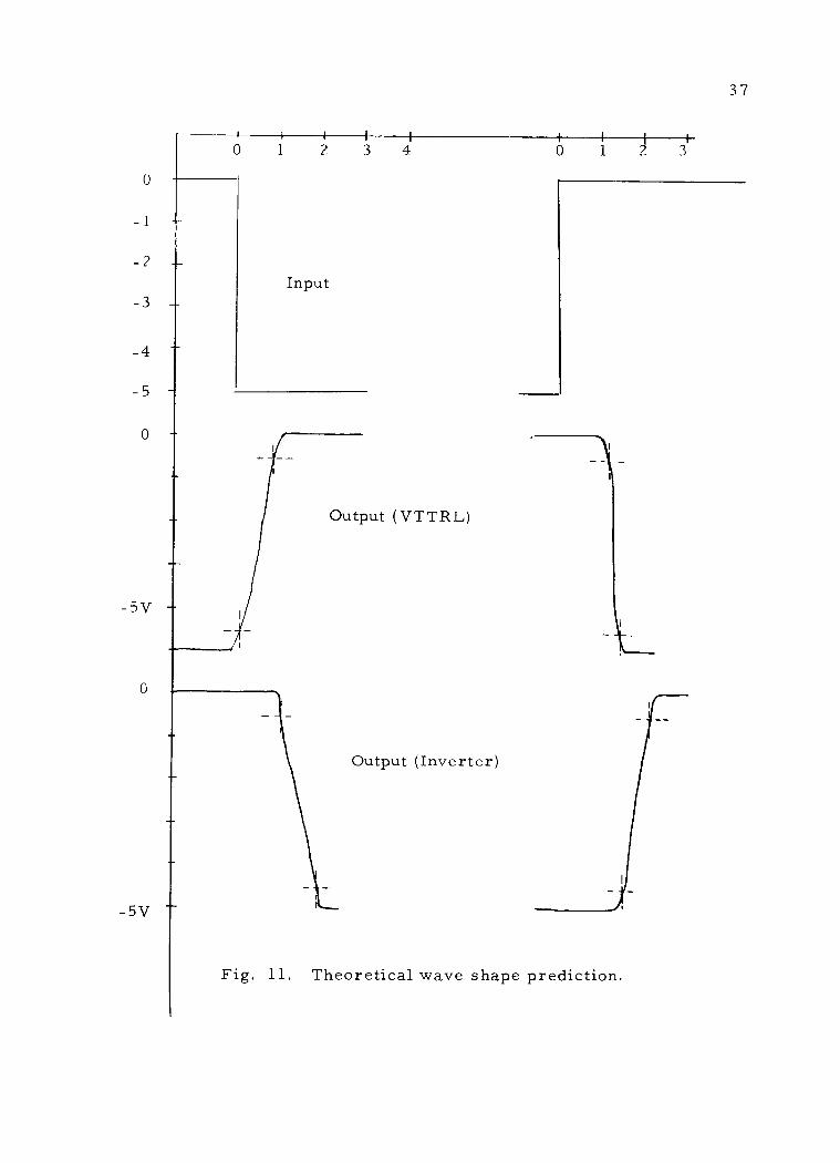
37
Fig. 11. Theoretical wave shape prediction.
-3 -

38 Fig. 11 shows the expected worst -case wave -shape at the output
of the inverter -stage without using speed -up capacitor.
In case of the output of the inverter, the calculated turn -OFF
time is 1. 60 4 sec. The observed turn -OFF time is 1. 20 p. sec. Con-
sidering that the turn -on time of VTTRL is actually O. 604 sec. corn -
pared to the worst -case turn -on time of O. 90p. sec. , the observed and
the calculated turn OFF times for the inverter stage are approximate-
ly equal. This implies that the tstora g e
and tfall of the inverter
stage, both calculated and observed, are equal. The turn -OFF time
is a maximum when two inputs are present in the VTTRL circuit.
For the maximum turn -on time, consideration is given to the
case (Figs. 14, 15) where all the three input are present in VTTRL.
The calculated turn -ON time is 2. 39 sec for worst -case. This in-
cludes the rise -time of O. 90 µsec. for the inverter stage alone. It
also includes the storage time of the VTTRL (Fig. 11), which for a
typical case is much less than the maximum storage time of 1. 11
4 sec. Because of these two considerations, the maximum turn -on
time observed is 1.40 µ,sec. as compared to the calculated value
(2. 394 sec. ).
The worst -case calculated total switching time is 4. Oµ sec.
The observed total switching time (maximum) is 2. 3 4 sec. The
switching times for different samples of 2N1305 were observed.
The total switching time varied from 2. 20 to 2. 50p. sec. Hence it
can be concluded that the total switching time for this circuit, with
the components used, can be assumed to be 60% of the worst -case
switching time.

Input
-5V
Output (VTTR
-5V
Output (Invt. )
_5
V
Output
Qvniiffi S.C.)
-5V
4 5 7
Ì
r
I I
I Scale: O. 2µs (cm
39
(A)
(B)
(C)
(D)
The flat portion of (B) is due to the delay time of the transistor (approx. O. 2µs).
Fig. 12. Observed response (one DC; one pulse input).
cm
1
I
1
I _ i
1
1
I I
1
1
I
I I
I
I

40
9cm.
-5V
--5V -1
-o
-5V
(A)
(B)
o
-5V
(C)
L_ I I
I (D) I
I
i i I Scale: O. 2µs /Fm
Due to the steep fall time, the reasonable frequency of lead inductance and stray capacitance is reached giving rise to overshoot. Fig. 13. Wave shapes for one D -C; one pulse input.
Of
3 4 5 6 7 8
-
I I
o
I
_f
Scale 0. 2 ps/cm
4 6
41
10m
0
Output
(VTTRL)
-5V
Output (Invert. )
-5V-
Output (Inverter with speed -up capacitor)
(A)
I I
I I
Scale: 0. 2µ s /cm,
II
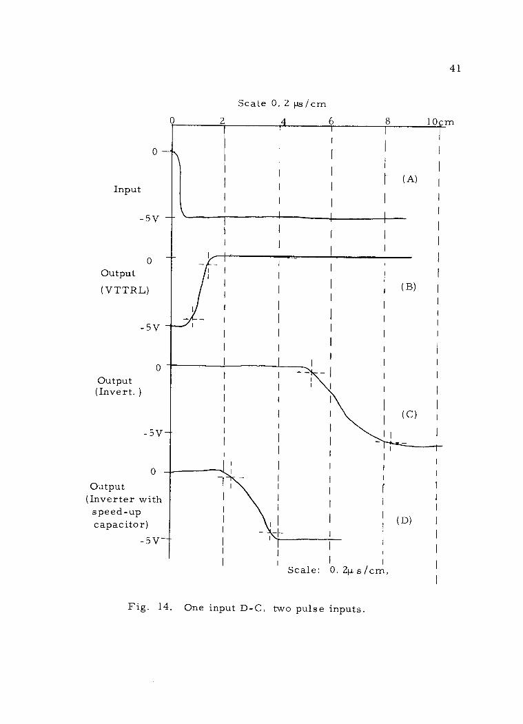
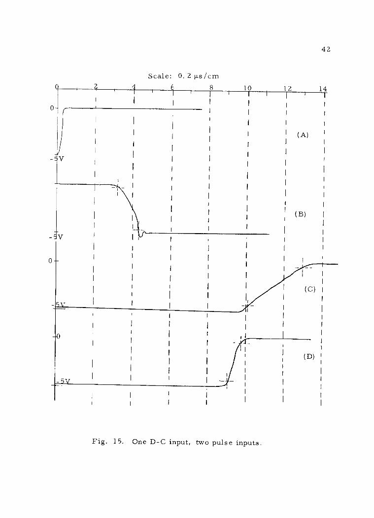
Fig. 14. One input D -C, two pulse inputs.
(B)
(C)
o --
-5V
1
1
I I
I I
I
1 1
I I
I I
I
I
I
I I
1
Input
-5V
Scale: 0. 2 µs /cm E 8 10 12 14
I
I I I 1 I
I I I I
I
I I ' I I 1
I I I I I I (A) I
-V i I I I
I
I I
I I I
I
I
1 I I I
I
_ I I I I '
I I I
I
I I I
I I I
I
I I
I ( (B) I
I I ' I I I _ 1
-V I I I I
I
I
I I I I I I I
I
i I I I I I
I I I I I
I
I I I I I i
I
I I I (C) I
_I I I I I I I
_ I I
1 1 I I I
I I I I I I I
I 1 I I r
I I
I
I I I I 1
i
I I II
I f I
(D)
I I I I
1 I
-5V I I
I - - I I
I
I I
1 I I
I I I I I
42
Fig. 15. One D -C input, two pulse inputs.
,
I
I
I -
I
1 1 !
i I
I
I
1
I

43
Transient Response Improvement Using Speed -Up Capacitor:
Typical base current (without CT)
5 - 0.35 15 +0.35 2. 90 15
= 1. 60 - 1.02
(Ib ) = 0. 59 mA 1 typ
also, I
(Ib )ì, = 0. 30 mA 1 /
In order to have a faster response, more turn -ON current must be
supplied during transient conditions. This will automatically result
in a high turn OFF current of opposite polarity during turn OFF
period. Thus the total switching time will be reduced.

44
Observed switching time of the output at the inverter stage as a
function of speed -up capacitor values is shown in Table VI.
Table VI. Switching times
Number Speed -up Capacitor
pf
td tr tf tf ttotal µs µ s µs µs µs
1 - 0.40 0.60 0.80 0.30 2. 10
2 100 0.40 0.20 0.65 0.30 1.55
3 250 0.40 0. 15 0. 50 0. 20 1. 25
4 400 0.40 0. 15 0.50 0.20 1.25
5 500 0.40 0. 15 0.50 0. 20 1. 25
6 1, 000 0. 40 0. 10 0. 40 0. 20 1. 10
7 1, 500 0. 40 0. 10 0. 40 0. 20 1. 10
8 3, 000 0. 50 0. 10 0. 35 0. 20 1. 15
9 10, 000 0. 50 0, 10 0. 35 0. 20 1. 15
C is chosen, equal to 1000pf. The total switching for this
case 1. 10 µ s.
Current supplied by RT = 1. 60 mA. Assuming that the capacitor
supplies 10mA of current in 0. 5 µ sec.
Ixot C = °V (19)

For a constant base voltage during switching the voltage
swing = 5V
C = 10x10 -3x0. 5x10 -6
5
45
C = O. 001 p.F
The transient current supplied by CT is assumed to be 6 times
that supplied by RT.
The observed values of Turn ON and Turn OFF times are O. 50
and 0. 60 µ sec respectively.
Hence by the use of the speed -up capacitor, the total switching
time of the combined VTTRL is made 1.40 p. sec (max. ) which is
comparable to the switching time of only the VTTRL stage.
The calculation of the exact value of speed -up capacitor is not
possible. Therefore a table (table VI) of switching time, using
various values of speed -up capacitor was drawn. It also gave
CT = 0. 001 p.F as the speed -up capacitor giving minimum switch-
ing time.
It can thus be concluded that the use of the speed -up capacitor
in the input of the inverter -stage helps in reducing the switching time
of the combined VTTRL- Inverter circuit, to that of an VTTRL circuit
alone. The total switching time is comparable to the switching time
of the transistor alone.
Effect of base current on switching time: Figs. 12, 13, 14,
and 15 show the transient response of the VTTRL- Invert circuit.

46
In Figs. 12 and 13, one pulse and one D -C input are present.
This results in a minimum base current, which makes the turn -on
time, large and the storage time, short.
In Figs. 14 and 15, one D -C. and two pulse inputs are present.
This results in a maximum base current, which makes the turn on
time, short and the storage time, large.
The fall time which depends on the turn -off current remains
almost the same in both cases.
The total switching -time also remains the same because in-
creased turn -on time results in a decreased storage -time and vice -
versa.

-E 1-
c_5V
Fig. 16. Transient response improvement using speed -up capacitors (INVT).
RT bi
47
Fig. 17. Variable threshold logic circuit.
N
a2
_I

48
PART III
CIRCUIT # 2
Variable Threshold Logic (Fig. 17) (4)
Here the transistor is kept forward- biased both in the worst -
case -OFF and worst- case -ON conditions. The input resistors
(RT) act as Kirchoff's adder, supply a definite input current for one,
two, or three inputs, (E c
volts).
The base - emitter junction forward -voltage, when the transistor
is OFF is determined by the small resistance Ro. During the OFF
state, all the current supplied by the input transfer - resistors passes
through Ro. The base - emitter junction voltage is determined by the
amount of current passing through Ro and the value of Ro. The base-
emitter-junction voltage should not exceed the minimum base turn -
ON voltage for the transistor used. In practice, this voltage is kept
much below the turn -on base voltage for the transistor.
For the turn -on condition, the base - emitter - junction voltage
should exceed the minimum base turn -on voltage, and there should
be sufficient current in the base -junction to saturate the transistor.
In this particular circuit, the fan -in is three. Two of the
three inputs are required to saturate the transistor.
o.

49
Important Parameters
(Vbo) Maximum base -OFF Voltage
Since in this case the base voltage is kept forward -biased with
respect to the base - emitter junction, it should not exceed the mini-
mum base turn -on voltage. Since the minimum base -on voltage is
not a well - defined parameter, the maximum base -off voltage is
kept much below the minimum base turn -on voltage under worst -
case conditions.
(Vbs' ) *: Maximum Base Turn -ON Voltage 1
During the turn -on condition, the current supplied by the
transfer- resistors is divided between the base - emitter junction
diode and R . 0
The higher the base voltage, the more current will
be taken by R 0
. Under the worst -case conditions, there should be
enough current through the base - emitter junction to saturate the
transistor.
(V ) . cs
discussed in VTTRL circuit
(h f e

50
(I co )*: Maximum Transistor Leakage Current
In this circuit there is no back biasing voltage to nullify the
effect of leakage current. Hence the maximum leakage current
should be very small.
However, it is assumed that the transistors used in this cir-
cuit have a high base turn -ON voltage. Also, there is a small re-
sistance (R ) 0
in parallel with the base - emitter junction.
Because of these two reasons, the effect of leakage current in
forward biasing the base - emitter junction and turning ON the tran-
sistor when it should be OFF is negligible.
It is however inferred that the transistors having a high base
turn -ON voltage have a low leakage current. Hence the effect of
leakage current can be neglected in this circuit.
Selection of a Transistor for VTL Circuit
The most important parameter in the steady- state, worst -case
design of the VTL is the minimum base turn -on voltage.
Since the transistor is not back -biased during the OFF period,
the base turn -on voltage has to be sufficiently high (greater than
0. 70 V), in order to have an adequate separation between the ON
and OFF conditions in the base circuit.
Due to the use of the small resistance (Ro) in the base circuit,

51
Table VII -A. 2N 2713 NPN silicon epitaxial transistor characteristics Absolute maximum ratings
Voltage Collector emitter VCEO
18V
Emitter to base VEBU 5V
Collector to base VCBO 18V
Current (collector) IC 200mA
Power dissipation P,,(25 ° C) 200mW
PT(55 ° C) 120mW Derate 2. 6 7mW / ° C increase above 25°C
Electrical characteristics (25°C) MIN TYP MAX
Forward current transfer ratio VCE = 4. 5V, IC = 50 mA)
hfe 30 60 90
Collector- emitter saturation voltage (I = 50mA IB = 3mA) VCE 0. 3V
Base - emitter saturation voltage (I = 15, IB = 0. 7 0. 9
Cut off: collector current C130
(25°C) 150°C
1.5µA
15 µA Input impedance
hf e 200 ohms
Switching times td = 60nsec IB = 3 mA
1
t = 85nsec r I = 3. 84 mA
t s
= 85nsec 2
tf = 40nsec
)
/

52
Table VII -B. Pre -assigned parameters
M 3
L 2
(V )* 0. 3V cs
(V b s I)* 0. 90V
1
( Vbo)* 0. 45V
IC) 15mA
(Ibs)* 15/30 = 0. 50mA
(hfe) * 30
(p)>, = (lb ) * /(Ibs)* 1
v C
Vbs( 3)
E1
E2
EC
1. 2
0. 60mA
0. O1mA (75°C)
0. 01V
0. 05mA
0. 1 volts
1. 0 volts
+12V
-12V
+6V
c
(Ib ).m
05 0
( Vcs)'' (I )x<
1

-1-(E 1
) *
(V ),, cs ' o
o (E ).,.
C
Fig. 18-A. Worst-case OFF condition.
(R T )
'
(\AA/ .1-
1 (R )...,
1 ' (V cs
s, (vbs)*
c
(I ),,, (I rc
Fig. 18-B. Worst-case ON condition.
(RT)*
N
53
V\AÌ f
(RT )':'
2
v)(')
7C 0/ 1,4N
bi
(E1)*
ó)y,

the effect of the leakage- current (I ) is negligible. co
The other parameter that is very important in the design is
(hfe) Also, for a particular transistor, (hfe) should not fall min
below (hfe),,, throughout the working life of the transistor.
A NPN 2N 2713 epitaxial silicon transistor was chosen for
realizing this circuit.
A 1N 50 clamping diode was used for clamping the output volt-
age.
Fig. 18 -A. Worst -case, OFF Condition
Node (1)
((Ec),,, + Vc ( Vbo)''`) ((V cs )*
- ( Vbo)^`) ( Vbo).,.
(Io)''` _ ;, (20)
In order that the transistor remains off,
(I )' = 0. 0
Node (4)
((E1).;: - (E ,)
(R1) ̀ ((Ec):;. - (Vbs'1)''`) X N
54
(21)
The values of the circuit parameters used in this circuit are
such as to turn the transistor ON. The collectors of the two preced-
ing ON stages are assumed to be at their maximum value and so is
-
-
- ( I )* + co (R ) -
(RT)* + (RT)'/2

55
the clamping voltage (E )
c of the preceding OFF stage. The values
of the transfer resistors (RT) are assumed to be minimum. The
base- emitter junction voltage is assumed to be at its maximum
allowable limit. The small resistance (R ) o
is assumed to be at its
maximum limit so that it takes least current. Under these circum-
stances it is assumed that the transistor is an open -circuit, and ti,
is no current passing through the base -emitter junction.
Worst -Case ON Condition (Fig. 18 -B) (Node 2)
The conditions are similar to that discussed for VTTRL col-
lector circuit.
The node equation is
((E1) < - (Vcs) *) ((Vb0)0 - (Vcs" (I I) _ (IRc) " + (R1)=;. (RT)'` /N
Node (3)
((Ec).;. - (Vbsli )''`) ((Vbs'l) '' - (Vcs).;<) (vbs1)"
(RT)::/2 (R + (Ibl):;
(Ro).
In the base circuit (node 3), two of the inputs are present
( +Ec volts), and one of the inputs is absent (approx. zero volts),
In this case, a forward current of enough magnitude to saturate
the transistor, has to be supplied to the base- emitter junction by
the two inputs that are present. It must also supply additional
current to (Ro), in order to keep the base- emitter junction at the
c

56
minimum base turn -on voltage, and a small current to one of the
inputs that is absent (zero volts). Hence the clamping voltage (E c) c
is assumed to be a minimum, and the transfer -resistors for the two
inputs, that are present, are assumed to be at their maximum value.
The base -on voltage is assumed to be at its maximum value, so that
the difference in input and base -on voltage is a minimum, resulting
in the least input current. The transfer -resistor of the remaining
input is assumed to be a minimum, so that it takes a maximum
current.
Solving equations (20) and (23) for the worst -case OFF and
worst -case ON conditions at the base - emitter junction, the two
equations are,
RT = f(Ro) = 9. 79/(0. 60 +0. 70 /R o) Tmax
R,I = f(Ro) = 11. 72 Ro min
The values of R and R for various values of Ro Turin Tmax
are tabulated (table VIII), and plotted (Fig. 19).
From the plot, a value of Ro and RT is chosen to obtain a
maximum tolerance limit for RT and Ro (table IX).
(24)
(25)
max

R o
Fig. 19. Tolerance of RT and Ro.
57

58
Table VIII. RTV is Ro
Number R° KS-2
RT min
KS-2
R Tmax KO
R T R max Tmin KS-2
1
2
3
0.050
0.100
0.125
0. 586
1. 172
1.465
0.670
1. 290
1.580
.084
0. 118
0.115
4 0. 150 1. 758 1. 860 0. 102
5 0. 175 2.051 2. 120 0.069
6 0. 200 2.344 2.380 0.036
7 0. 225 2.637 2.630 -0.007
8 0. 250 2.930 2.880 -0.050
9 0. 275 3.223 3. 100 -0. 113
10 0.300 3.516 3.330 -0. 186
Though the tolerance limits for lower values of R,T and Ro
are more, choosing a low value of RT will increase interactions
between various input.

59
Table IX. Circuit parameter tolerances
Point Ro Permissible RT Permissible Nmax Permissible on tolerance tolerance N Fìg, ohms
of R K SZ
of RT %
o T
1 147 4. 75 1. 800 2. 77 2. 72 2.0
2 175 3.60 2.085 1.68 3.30 3.0
3 200 2. 50 2.360 0.96 3.64 3.0
Hence VTL circuit with
RT = 2. 085 ± 1% K S2
Ro = 175 ± 3% ohms
R = 0. 775 ± 3% KS2
N = 3 max
El = 12± 1%
E c
=6V 1%
is chosen.
As the oscilloscope amplitude calibration is accurate to f 3 %,
it was impossible to obtained the required ± 1% voltage tolerance.
The increased voltage -tolerance was, however balanced by reducing
the tolerance of RT and Ro to ±1 %. The value of Ro was especially
very critical in the working of VTL circuit. Voltage -levels were
adjusted to less than ± 1% using precision D. C. voltmeter and D. C.
inputs. It was observed that under typical conditions, the circuit
o Max
19
o

worked with about ± 3% voltage tolerance. However, in a worst-
case condition, ±1% voltage tolerance will be required.
Maximum Power Dissipation
(E 2
max(ON) (R1)'1: ((Ec)2--)
P (E1)''` ((E 1)* - (Ec) - N
max(OFF) (R1).., (RT)''`
P max(ON) = 200 mW
Pmax(OFF) 67. 4 mW
60
(26)
(27)
Due to the absence of the back -biasing current source (E2 -R2),
the power dissipation of an off transistor is comparatively small.
This is one of the important advantages of this circuit.
Transient Response
Some additional parameters have to be determined in order to
predict the transient response.
(1) Maximum base -ON current: (Fig. 20)
Here the base -voltage is assumed to be the maximum (all the three
inputs are present). The value of the transfer -resistors is a mini-
mum. The value of Ro is at its maximum. (Ibm) is calculated
from the base node equation (28).
3((Vco) - Vbs(3))
(Ibm) (RT,)., (Ro)* (Vbs(3))
(28)
1)*
=
-

+( Vco)*
o Vbsi 3)
I = II + III
Fig. 20. Maximum base ON current.
I + II = III + IV
Fig. 21. Minimum available Turn -OFF current.
61
(RT);<
Ì IpI
IÌI
(

62
(2) Minimum Available Turn -OFF current (Fig. 21)
This current is calculated immediately following (Ib)''` Hence
the base voltage is assured to be V ' bs (3)' Under these conditions
the current going out of the node through R ,
0 and preceding ON
stage is larger than the current flowing into the node due to the
preceding OFF stage. This results in a transient back -biased cur-
rent flow into the base emitter junction.
"co)* - vbs (3)) Vbsj(3) (Vbs1(3)-(Vcs) ̀ ) -(I2')
' (RT);, (Ro)'' (R,,) ;./ 2 (29)
From the present calculations, it appears that the turn -OFF current
is not reduced very much because of the absence of the back- biasing
current source. The small grounded resistance (R ) 0
supplies
enough base turn -OFF current.
Design of the Inverter Circuit
The design of the inverter- circuit for VTL will be similar to
that for VTTRL. A back -biasing current source (E2 -R2) is neces-
sary to limit the base current in the Inverter. The circuit diagrams
and the node equations are similar to those for the Inverter circuit
previously designed, and are therefore, not repeated.
The values obtained are:
RT = 2.085± 1% K
_ -

63
(R2) = 54 K max
(R2) = 7.45 K min
(R 2) = 7. 75 K4: 5% chosen
R1 = 820 ohms
N max = 2.62
(N ) =2.0 max permissible
R2 is chosen close to (R2) in order to avoid large base min
turn -on current.
Transient Response
The calculated values of the minimum base turn -OFF current
(I2') , and the maximum base -ON current (Ibm) < are:
(1) For test circuit (I c
= 50 mA)
(Ibm);: = 3 mA
(I2') = 3. 84 mA
(2) For VTL circuit (1c = 15 mA)
(Ibm)* = 4. 55 mA
(I2'),;(= 1. 80 mA
(3) For Inverter circuit (I c
= 15 mA)
(Ibm).,, = 1. 07 mA
(I2')* .= 1. 05 mA

Using the switching equations of Appendix I and the above
values, the worst -case switching times for the designed VTL and
inverter circuits are calculated. They are shown in table IX.
Figs. 22 and 23 indicate the observed wave shapes. The
peed -up capacitor (O. 001 µF) improves the performance of the
ïrcuit considerably.
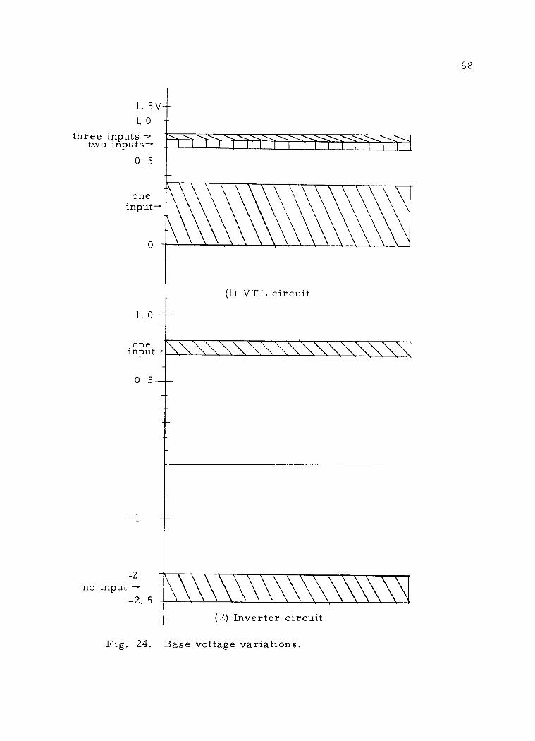
Fig. 24 indicates the tolerances of the base voltage for one,
_wo and three inputs.
The comparison of the calculated and observed switching -times
is shown in table X.
For the VTL circuit, the worst -case total switching time is
625 nsec. the observed total switching time for
1) one D. C. , one pulse input is 430 n secs
2) one D. C, , two pulse inputs is 510 nsecs
Because the Data -Pulse has 50 nsecs of rise and 50 nsecs of
fall time, the observed switching times are longer than they would
;e if a step -input pulse was used.
Rise -time. The observed rise -time (maximum) for one D. C.
and one pulse -input is 100 n secs. The calculated maximum is
145 n secs. This difference is due to a larger turn -on current
compared to the worst -case value.
Storage -time . The observed storage time (maximum) for one
D.C. and two pulse inputs is 370 n secs. The calculated value is
rJ :

65
Table X. Comparison of switching times
td
ns -.
tr n s
t s
ns tf
ns ttotal
ns
Type of Wave -shape
60 145 370 36 625 Calculated VTL output for step -input
60 145 150 50 405 Calculated Inverter output for step -input
50 - 50 Pulse input (from data -pulse pulse generator
one D. C. , 80 100 200 50 430 VTL output (obs) one pulse
input 320 110 310 40 780 Inverter output
120 20 100 50 290 Inverter output with 0. 001 [IF speed -up capacitor
one D. C. 60 40 370 40 510 VTL output (obs. )
two pulse
inputs 500 100 210 40 850 Inverter output
425 25 120 30 600 Inverter output with 0. 001 ¡IF speed -up capacitor
i

+6V
Inpu
OV I
+6V
Outp t
freq = 500 kc, P. W. =
scale 0. 1 µsec /cm (1) one D. C. , one pulse
5 6r
(VT )
+6V
Outp t (.Inv-rter)
OV
+6V
L_
5
66
Outp t Inve ter I
with speed up c : paci
OV
I
Overshoot is caused due to the resonance frequency of lead inductance and stray capacitance which coincides with the operating frequency of the circuit when the rise or fall time become very small.
Fig. 22. VTL circuit wave shapes.
1 µsec.
input
1
i
I I I
I I I
1 I
i I I ' I I
1
I '
I
I
I I
I
I
I
I
I
I I
I I-
I
oV
I Il I i
1 I 1 I I
1 i I
l 1
1
I I
I I I
I 1 I I I
I
I
I I 1
Il I I
I I I
I
i ¡ I
I
i I
I
I I
Ì I
I I i
1
I i
I I-- I
I ¡
1

67
_ +6V1
6V1
+6VI II
Ou put (V L)
(
1
1
i
Outpút Inventer)
I 11 1
ov 1
1
+6vI 1_
Dutpút Invek r)
With eed-up zapac) or
0 -
1
Scale: O. 1 µ sec /cm Fig. 23. VTL. One D.C. input, two pulse inputs.
I
I
_ o v- - -1
I
-+6vI
i
I
I
1
I
I-
1
1
1
I
1 1
1
np
I I
I
I
I
I
68
1. 5V 1. 0
three inputs - two inputs
0. 5
one input
1. 0
one input.>
0. 5
-2 no input ---
-2.5
`t_\\\'\\\\t\\\ M111111r11111111111111MINE
(1) VTL circuit
ilR\ \\\\\\\
1 I kW= IL 1k 1 (2) Inverter circuit
Fig. 24. Base voltage variations.
-
-
-.

69
370 n. secs. This is because the worst case and the typical maximum
ON currents are approximately equal in this circuit.
Fall -time . The observed and (for the same collector current)
the calculated fall times are equal (50 n secs) because the turn OFF
current in the two cases is almost identical (for the same collector
current).
The total maximum switching time (510 nsecs) is larger com-
pared to the test circuit value (270 nsec. ). The increase is mainly
due to increased rise -time (about two times) and increased storage
time (about four times). The rise -time increase is due to the
smaller minimum turn ON current. The storage time increase is
due to a larger maximum turn -on current.

70
PART IV
CIRCUIT #3 (4)
Transistor Tunnel -Diode Resistor Logic (TTDRL)
The design of the VTTRL and VTL is mainly based on the
threshold- effect. A minimum base -ON voltage and a minimum base -
on current is required to turn the transistor ON. By using a back -
biasing current source (E2 -R2) in VTTRL, and by using a small
resistance (Ro) in VTL, the parameters of the circuit are so chosen
as to keep the transistor OFF with one input present (equal to -E c
volts) and just turn it on with two of the tree inputs.
The thresholding effect can be enhanced (4) by the use of a
Tunnel -Diode in the base of the transistor.
However a number of problems have to be solved before the
use of the tunnel diode in this circuit is justified. The problems
are:
1. The peak current of an ordinary tunnel -diode varies by
almost ±10 %. The best tunnel- diodes available have a peak current
tolerance of ±2. 5 %.
2. (Fig. 24 -B) represents the characteristics of the base -
emitter junction of a transistor superimposed on the tunnel -diode
characteristics, assuming that no back -biasing current source is

5--
9
8
two input
| r 1-
71
100 200 300 400 500 B
Tunnel-diode characteristics M.V
inputs ____ three npuze_-__-_ ^-tzzunol-diodo
/ characteristics
two inputs -------_- `
e | | -n --- - C one input _ - - _ _ _ -- _ _ - - --
base - emitter junction ` '-- actually kse,., ` (Tunnel-diode) characteristics (NPN `
` transistor) c -~-aeeozoed (base- emitter junction characteristics)
Fig. 24.
100 200 ---
1 | t -T
400 500 600 D
Tunnel -diode characteristics (with 100 ohms ru parallel resistor). -
6-
,r l
6
--
one input_
-t-
- -
e
-0 T. D
0 A
-to
I I I I
300
G, 4
I --i I h
Tn `eflonr

72
applied in the base circuit. Upon applying one input, the stable
points are (a) and (c). Since the tunnel -diode is at its low voltage
state, the stable point is therefore, (a) in this case.
Upon applying two inputs, the peak current point of the tunnel -
diode characteristics is just reached and now the stable point is (e)
in the high voltage region. Due to the high voltage, the base - emitter
junction of the transistor is forward biased. If sufficient current is
pumped into the base - emitter junction, the transistor turns ON.
However, upon removing one of the two inputs, the stable
point is (c) in the high voltage region, which keeps the transistor
ON.
(3) When the tunnel -diode is in the high voltage state, the
stable points (e or c) are such that the tunnel diode takes very small
current, thus deeply saturating the transistor. This results in an
increased storage time for the transistor.
Possible Solutions
(1) In order for the tunnel -diode to return to its low voltage
state when the number of inputs present (equal to -E c
volts) decreases
from two to one, the base - emitter junction characteristics should not
touch the high - voltage positive region of the tunnel -diode when only
one input is present. This can be accomplished (Fig. 24 -C) by
connecting a small resistor in parallel with the tunnel- diode. The

73
100 210 300 410 500
Fig. 24 -F. Tunnel -diode characteristics (with 82 ohm parallel- resistor).
0 100 200 300 400 500
Fig. 24 -G. Tunnel -diode characteristics (with 60 ohms parallel- resistor).

74
combined characteristics are shown in (Fig. 24 -D).
Due to the shape of the tunnel diode characteristic, the bias
of the base -emitter junction characteristics should be below (I ') v min for one input present and equal to (I ') for two inputs present.
p max It is practical to design such a circuit if the fan -in is three
and the threshold value is two. However, it is not feasible for
larger fan -in.
The other advantage of using a parallel resistor is that the
combined tunnel- diode, and resistor characteristics takes appreci-
able current in the high voltage state, thus reducing the saturating
current in the base - emitter junction.
(2) For fan -in greater than 3, a reset pulse has to be used
for the tunnel diode threshold. It is claimed (4) that a circuit with
51 inputs was built utilizing tunnel diode threshold effect.
Selection of a Transistor for T'TDRL Circuits
(1) From the 'Steady- state" point of view: The minimum
turn -on base voltage of the transistor should be large compared to
the peak- current voltage of the tunnel -diode (V ), in order to keep
the transistor OFF under worst -case conditions.
The minimum base turn -on voltage should be of such a mag-
nitude that when the tunnel diode switches to the high voltage state,
the base - emitter junction characteristics (Fig. 24 -D) should intersect

75
the tunnel diode characteristics in the high -voltage region. If this
condition is not satisfied, the high-voltage stable point cannot be ob-
tained.
The value of the minimum base turn -on voltage should be near
the valley -point tunnel -diode voltage (Vv), to facilitate this.
The value of the base- emitter junction voltage is determined
by the point of intersection of the tunnel- diode, and the base - emitter
junction characteristics. The input biasing current shifts the base -
emitter junction characteristics up or down, depending on the value
of the biasing current. The maximum base ON voltage is thus lim-
ited by the maximum allowable voltage on the tunnel -diode character-
istics.
The specifications regarding (hfe ,,, and (Vcs)''` are the same as
for VTTRIr,.
The effect of leakage current (ICBQ)* is negligible due to the
presence of low resistance tunnel -diode in the base circuit.
(2) From "transient- response" point of view: Since the tunnel
diode switches very rapidly from low -voltage to the high - voltage
state, the transistor used in this circuit should be a high -speed
transistor.
The transistor chosen for this circuit is 2N96 7 which has a
total switching time of 180 nsec.
The tunnel diodes used are IN 2941 and 1N 371 7. Both have
76
the same characteristics. The peak current tolerance for 1N2941 is
± 10% while that for 1N3 71 7 is ± 2. 5 %. A tunnel diode with a high
peak current (4. 7mA) was chosen because the tolerance limit re-
quired for a low peak current (1mA) tunnel diode were very severe,
especially after connecting a parallel resistance. However, if a
low peak current tunnel diode is used, it will take smaller current
which will result in a higher value for the transfer resistors and a
greater fan -out.
Selection of a parallel resistor for the tunnel diode
The parallel resistor has to be of such a magnitude as to lift
the valley point of the combined tunnel- diode, parallel -resistance
characteristics above the base - emitter junction characteristics in
the presence of one input.
100 ohms, 82 ohms, and 70 ohms resistances were tried.
The combined characteristics with the tunnel -diode was plotted with
the help of Tektronix 545 curve- tracer and are shown in Fig. 24 -D,
24 -E and 24 -F.
Calculation for RT and Nmax were made for various values
of circuit parameter tolerances using the combined characteristics
of the 100 ohm and 82 ohm parallel resistors. Since the new valley
point tolerance depends mainly on the tolerance of the parallel
resistor, 1% tolerance limit is put on these resistances. Table XII

77
Table XI(A). 2N 967 PNP Ge transistor
Absolute maximum ratings Collector base voltage
Collector emitter voltage Emitter base voltage
Collector current Total power dissipation
CBO
VCEO
VEBO IC
P(25°C Air)
P 25 T(
°C
Free
case)
12V
12V
1. 25V
100mA
150mW
300mW
Electrical characteristics MIN TYP MAX
Collector -base breakdown voltage le = 100µA, IE = 0
BVCBO -12V Emitter base breakdown voltage
IE= 100µA, le 0 BV EBO -1. 25V
Collector cut off current ICBO -5µA. Base -emitter sat. voltage
IB = 1mA, le = -10µA VBE
sat. -0. 3 -0. 5V
Collector- emitter sat. voltage ID = -1 mA, Ic = 10mA
VCE sat. -0. 2V
Static forward current transfer - ratio (VCE = 1. 3, Ic = -10mA) 40 80
Switching times for I = -10mA, I = -1 mA = c B(1)
I B = 0. 25, VBE = 1. 25V (2) (OFF)
RL = 300 ohms
tON
tOFF
60 nsec 120 ns
MIR

78
Table XI(B). Preassigned parameters
M 3
L 2
(V )* -0. 2V cs
( Vbs -0. 5V 1
(I ) 15mA
(Ibs) 0. 375mA
(hfe)* 40
(P),, 1. 2
(Ib ),;, 0. 45mA 1
(Vcs)'` 0. 01V
(lb)* 0. lmA
(I ) * 0. 05mA rc
v c -0.1V
Vbs -0. 5V
El -12V
E c -6V
3)

79
shows the calculated values.
Steady -State Calculations
The conditions for the worst -case -OFF state junction charac-
teristics does not touch the high voltage region of the tunnel diode
characteristics. In other words, the bias current for one input
should be less than the valley -point current of the tunnel diode
characteristics.
Due to the presence of the tunnel diode, the transistor can
never turn on (if the tunnel diode is in its low voltage state), in the
presence of just one input, because the bias current under the worst
conditions is about half of the peak- current.
However if the tunnel diode is switched to the high -voltage
state by the presence of two or more inputs, then the tunnel diode
will return to the low- voltage state when all but one input is removed,
only if the base - emitter characteristic does not touch the high -volt-
age region under this condition. This condition is satisfied by con-
necting a parallel resistance to the tunnel diode.
Here the design procedure is as follows: The transfer resis-
tor is chosen from the worst -case ON condition alone. It is chosen
such that under worst -case ON conditions, the input current is just
sufficient to cross the worst -case maximum peak current of the
combined tunnel- diode, parallel- resistor characteristics. This

r RT s al
2
L r RT Dl
RT s
RT
D
TD
TTDRL Inverter
Transfer -resistor for TTDRL M Number of Inputs (3 in this circuit)
Input- resistor for Inverter L Threshold level (2 in this circuit)
Clamping diode
Tunnel diode N Number of outputs to be optimized
Rs Source impedance of inputs
Fig. 25. Transistor tunnel -diode circuit.
RT
a
w

81
value of the transfer resistor is substituted in the worst -case -OFF
conditions and the maximum input current pumped into the tunnel
diode under these conditions is calculated. If the value of this cur-
rent is less than the valley current of the combined tunnel- diode,
resistance characteristics the design is valid. Otherwise the pro-
cedure has to be repeated for various values of parallel resistors until the above conditions are satisfied.
Worst -case, OFF Condition (Fig. 26 -A)
The maximum value of the tunnel diode resistor characteristic in the high -voltage state is V '. Assuming this as the worst -case
OFF base voltage, and maximum input current, the current pumped
into the tunnel diode is calculated. It is also assumed that no cur-
rent flows through the transistor. This current should be less than
the valley -point current of the combined tunnel diode, resistor char-
acteristics in order to have the mgnostable circuit operation.
For node (1) the equation is
((Ec)' + (vc) - V p
) 2((Vcs)* - (V )) P
(ITDL) (R,,)<,- + (R,,),.
For node (2), the equation is
((E 1)* - (Ec),:) ((E ):44 - ( Vbs 1) `)N
(R1), _ (I co) + (R,I,)
(32)
(33)
+
c

-(V ).,. cs O (RT)'/N
O-Mn,
82
I 1
-Ec+vc (RT)* TD R IV D
T T V= VI+VII III
I=TI+III+IV -(Vcs)-,< (RT)* o ^M,
---- II
I
o -(Ec),4
-(V ):;.
T IV
TDL
I
o(E1)
VII t
IX ( T
N Vbo), VIII
IX +X= VII +VIII
1
Fig. 26 -A. Worst -case OFF conditions. B. Worst -case ON conditions.
( -E, ).x
*
A
(RT)*/2
co
(R.I,)'x/2
B
1

83
Worst -Case ON Conditions (Fig. 26 -B)
The base node equation is written under the following condi-
tions:
The input current supplied by the transfer resistors is a
minimum. In other words, the input voltage is at its minimum val-
ue and the transfer resistors are at their maximum value.
The tunnel diode, resistor combined characteristic has a
maximum peak current value.
The bias current due to the inputs is just sufficient to cross
the maximum peak- current value.
Since the tunnel diode switches very fast to the high voltage
state from the low voltage state, and takes less current in the high
voltage state compared to its peak current (Fig. 24 -D), the current
required to saturate the transistor is not added to the peak current
of the tunnel diode, resistor. The difference between the peak -
current and high voltage state current is sufficient to saturate the
transistor.
The node (3) equation is:
((Ec),;< - (Vbsl)) x 2 (Vbsl) - (Vcs),;`)
(RT)* (Ibl)''` + ( (RT)=; + (ITDL) (34) -

Table XII. Effect of parallel- resistor, parameter tolerances on the working of the TTDRL circuit (I
c = 15mA)
Parallel- resistor
T. D. Peak
RT, ToL of
Tol. of
Worst- case
I Will the
Nmax R ±5%
tolerance %
cur:- rent tol. %
KO RT
%
volt- ages
%
I TDL per miss- ible
cir- cuit 21é
perm.
100 ohms 1%
2.5 1.99 1 1 3.25 3.40 yes
10 1.85 1 1 3.48 3.40 no
2.5 1.94 3 1 3.40 3.40 yes
2.5 1.90 5 1 3.50 3.40 no
3. 0 0. 725
84
82 ohms 2. 5 1. 88 3 3 3. 50 4.07 yes 2 ± 1%
10 1. 76 3 3 3. 74 4. 07 yes 2
2.5 1.86 5 3 3.66 4.07 yes 2
10 1. 74 5 3 3. 74 4.07 yes 2 0. 825
2.5 1. 78 5 5 3.92 4.07 yes 2 0. 830
10 1. 66 5 5 4. 20 4. 07 no
For the present circuit, RT = 1. 78 ± 5% was selected with
power supply tolerance oft 5% and tunnel -diode (1N3717) with ± 2. 5%
peak -current tolerance.
1
.c

85
The node equation for the collector is similar to one for VTTRL,
and is not discussed in detail (node (4)),
(I) = (I)* + c RC (R1).;. (RT) </N
((El)-, - (Vcs)''') ((Vbo)" + (Vcs)*)
Design of the Inverter Circuit
(35)
The design of the inverter circuit for TTDRL is similar to that
for VTTRL and VTL. A back -biasing current source is necessary to
limit the base current in the inverter circuit.
The circuit diagrams and the node equations are the same as
for the inverter circuits, previously designed, and are therefore not
repeated.
The values obtained are:
Assuming RT = 1. 78 + 5%
(RZ) 41.6 KO max
= 5. 45 'KO R 2) min
In order that base is not heavily saturated, R2 is chosen close
(R 2) min
R2= 5, 8 ± 5%
R1 = O. 790 KO
Nmax = 2. 08
Npermissible 2' 0
to
-

86
Transient Response
The values of (Ibm)* and (I2),;< are calculated as in case of the
other circuits.
Transient Response (TTDRL)
Maximum available turn -ON current and minimum available
turn -OFF current have to be determined in order to calculate the
switching times.
(1) Maximum base -on current (Fig. 27 -A) Maximum base -on
current is the difference between the maximum input current and
minimum current taken by the tunnel -diode in its high voltage state
(Fig. 27 -B). It will also depend on the base -emitter- junction char-
acteristics. Since this characteristic is changing within a certain
tolerance (e. g. base turn on voltage for I c
15 mA, varies between
0. 35 and 0.45 V), it is difficult to determine the exact current taken
by the tunnel diode.
The maximum input current calculated is 10. 3mA. The cur-
rent taken by base- emitter junction is calculated as follows:
Assuming turn on voltage (base = 0. 45V
slope of the base -emitter diode N 20 SZ
(0. 50-0. 45)x 103 mA steady state tunnel diode voltage - 20
= 2. 5 mA.
=

8`l
-( V )> co
A
(RT)''` -(Vbs' ) 1
Td IV
I = II + III
(Vco)° (RT).,
O r 1NN
C
40---- I Vbs(3)
(RT); -(Vcs)
o v
I+IV=II+III
B
V x = base ON current for
three inputs
y = base ON current for two inputs
Fig. 27. (A) Maximum base ON current (B) Base ON current determination (C) Minimum Available Turn -OFF current.
3
I ITDL (Ibm)''` /

88 This is one of the advantages of the TTDRL circuit. Irrespec-
tive of high input currents, the base - emitter junction current does not
become very high due to the presence of the tunnel -diode and parallel resistor in the base node. Also the minimum on base current is much
higher than the one required to just turn -ON the transistor. This re- duces the turn -on time.
Minimum Available Turn -OFF Current (Fig. 27 -C)
Assuming that the tunnel -diode is just shifting from the high to
the low voltage state, it has current of 4. 0 mA (82 ohm parallel re- sistor).
The nodal equation is
((Vco))c Vbs (3)) (Vbs'(3) - (V V') (36) -(ITh2 ) >;<
_ ITDL - (RT) ( )
It is assumed that the fall in the tunnel -diode voltage in the high volt- age stage towards the valley point is much faster compared to the
transistor switching. Then for transient considerations, the valley
point is assumed to be point under consideration.
(12'4 is found to be 0. 92 92mA.
(Ibm)* = 2. 5 mA
(I21)>;. = 0. 92mA
(Ibm)* = 0. 74
(I2') =2.37
` 1. 0
(I2') = 0. 50
4
TTDRL (Ic = 15 mA)
Inverter (Ic = 15 mA)
Test circuit (Ic = 10 rnA)
The switching times are calculated using Appendix I and are tabulated in table XIII and compared with the observed switching times.
- co cs (RT).x
(Ibm) r

89
Table XIII. Comparison of switching times
td tr is tf ttotal Type of wave -shape ns ns ns ns ns
20 80 106 36 242 Calculated TTDRL output for step input
20 160 54 20 254 Calculated Inverter output for step input
80 40 Pulse input
One D. C. , 120 80 80 60 340 TTDRL output (obs. )
one pulse 120 40 130 70 360 Inverter output (obs. )
input 80 30 100 70 21'0 Inverter output with 0. 001 µ F speed -up capacitor
One D. C. , 70 40 80 100 290 TTDRL output two 140 20 120 50 330 Inverter output pulse inputs
100 40 60 80 280 Inverter output with 0. 001 µ F speed -up capacitor
The calculated times are less than the observed values mainly
because in calculations, a step -input pulse is assumed. In the pres-
ent circuit, the input pulse has a 80 ns Rise and 40 ns fall -time. The
output of the Inverter seems to be as good as the output of TTDRL.
This is because the effect of the rise and fall time of the input on the
Inverter stage is much less than its effect on TTDRL. TTDRL re-
quires input voltage pulse of exact magnitude ( -E c
)V before the tran-
sistor can turn -on.

90
Output Inverte
Output Inverte (0. 001 F speed- p capacit r)
-6V
Scale: 40 ns /cm
1
An overshoot at the Inverter output is observed due to the presence of high turn -on current.
Fig. 28 -A. TTDRL circuit (one D. C. , one pulse).
Output
(TTDRI )
-6
o
Input

Input
-6
0
Output (TTDRL)
-6V
0
-6V
0
-6V
91
Scale: 40 n sec /cm
Fig. 28 -B. One D. C., two pulse inputs.

92
PART V
COMPARISON OF VTTRL, VTL, TTDRL CIRCUITS
(1) Circuit Parameter Tolerance
VTTRL . It is not practical to design a three input Majority-
Logic circuit with more than 3% tolerance limit. It is also not
practical to design majority circuits with more than three inputs.
VTL. The tolerance limits are more severe. The voltage
supply is assumed to be ±1 %. Other circuit parameters must be
more than t3% accurate.
TTDRL. As far as the worst case OFF condition is concerned,
the tolerance limit for this circuit can be increased much more than
the first two circuits. However in order to avoid the use of a reset
pulse for three input case, the tolerance limits have to be kept at
± 5 %. It is possible to design majority gate with five or more inputs
but the use of a reset pulse then becomes essential.
(2) Transistor Type
VTTRL. Can be designed using any kind of transistor, once
the (h ) is known. There are no special requirements for fe minimum the transistor to be used in this circuit.
VTL. Only transistors with a high base -ON voltage can be
1-
used in this design, because no back -biasing current source is used
here.
TTDRL. The transistor type is dependent mainly on the
93
tunnel -diode characteristics. The parameter of most significance
here is the minimum and maximum base ON voltage, and the base -
emitter diode characteristics. The base- emitter characteristics
should intersect the tunnel -diode characteristics at the specific
points in the presence of one, two, and three inputs. This is im-
portant to avoid heavy saturation of the transistor and to have proper
circuit operation without the use of a reset pulse.
The tunnel -diode characteristics can be modified by the use
of series and /or parallel resistance with the tunnel- diode. The
parallel resistance is required in order to have the proper circuit
operation. Hence in order to avoid extra tolerance because of the
series resistance, it is desirable to have a transistor with a base -
ON voltage approximately equal to the valley point tunnel -diode volt-
age.
(3) Cost
One important cost factor is the transistor type. The second
is tolerance limits of other circuit parameters.
VTTRL and VTL require components with more rigid tolerance
and TTDRL with comparatively less. But in TTDRL the additional

94
cost of the tunnel -diode has to be taken into account.
The type of transistor used in each circuit will be cheap or
expensive depending upon its maximum power rating, switching
speed, reliability of its parameters, etc. and therefore cannot be
considered separately for each circuit.
(4) Switching Times
VTTRL. Here the maximum base -ON current will be increased
if parameters of low tolerance are used and vice -versa. The turn -
OFF current should be large due to the presence of the back -biasing
current source.
VTL. Here the turn -ON current (maximum) is comparatively
more due to the absence of any back biasing source. However the
turn -OFF current is comparative to the VTTRL. This current is ob-
tained due to large current flowing through R (Fig. 17) when the 0
transistor turns -OFF from maximum saturation limit.
TTDRL . The use of the parallel resistance with the tunnel -
diode passes an appreciable turn -ON current for two out of the three
inputs and does not increase the turn -ON current too much when all
the three inputs are present. However if no parallel resistance
is used the maximum turn -ON current is very high. Also the
parallel- resistor has to be properly selected in order to obtain the
best switching times.

95
(5) Power- Dissipation
Due to the absence of the back -biasing current source in VTL
and TTDRL, their power dissipation for a particular value of maxi-
mum collector current is less than the power- dissipation for VTTRL
circuit.
96
BIBLIOGRAPHY
1. Akers, Shelden B. and Theodore C. Robbins. Logical design with three -input majority gates. I. Computer Design 2:12 -19. March 1963.
2. Mano, M. Morris. Designing transistor switching circuits. I. Steady -state analysis. Computer Design 2:28 -31. June 1963.
3. Richardson, D. W. Predicting transistor switching time. Mas- ter's thesis. Corvallis, Oregon State University, 1964. 72 numb. leaves.
4. Sauer, W. A. Majority and threshold logic. Electronics 36: 23 -24. Nov. 29, 1963.
5. Teoste, Rein. Digital circuit redundancy. IEEEE. Transac- tions on Reliability R-13:43: June 1964.
6. Wray, W. J. Worst case design of VTTRL circuits. IRE. Transactions on Electronic Computers II:382 -390. 1962.

APPENDICES

97
APPENDIX I (3)
Predicting the turn ON and turn OFF times under given current
conditions of the circuit using the typical switching characteristics
given in the specification sheet under certain curent condition.
Let the subscript o represent the conditions specified in the
specification sheet and the subscript 1 represent the conditions of
the circuit for which the switching time need be found.
(1)
t r1
RISE TIME:
ß T1
(Fig. 29)
1. 25 1. 7 RL CC )in ßC1
1- WT
+
1 1 1
ßT 1 t r
o
P T
1. 25 1. 7RL CC fnl-
PC o
+
WT Lo C1 ß T o o o
t
t 11 = KBK,TKC r 0
ßT K = 1 - 1.0
ß T o
1. 25 WT 1.7RL
C1 T1 1
KT W 25 + 1 . 7 RL Co T o
0
(37)
(38)
(39)
+
ry 1
I

K _ x
Y
y v/s x is plotted on a graph for different KC. Knowing
n y, KC is determined.
Fall Time (Fig, 10)
\ PCC
tf W25 + 1.7 RL C1 ßn 1+
1
fl 1 Tl t ßT1
tfo ß W
25 + 1.7 RL Co fn 1+ßCC T T o 0 o
tf 1
Kß T KK t C f 0
K =K ---1 p T
in l+RCC
PT1 KC =
PCC 0 j+ß
T o
r
T
Knowing x , y, KC is determined from the graph of
for various values of K.
(40)
(41)
(42)
(43)
98
To i
ßT
1
I ß 0
C y

C
.05
.01
99
10 1<c
iranworirm IMA/111/1M111 44 A r rOPIPAI
A Adi MIMI As =For ArdrawAsimme
4.011FAIr411 lur-416pArAgEri. A,.."1,410011/41.11"
r-Pr V Pr
A-d A A .01
Fig. 29.
.05
/ CO
PTO
Plot for finding Kc of the rise time equation.
.5
grariffor rApj
V Bar FA mgdwAnskil A AreArarivAirAmimm IAMIIIIMIWAPA
owdor II ßT
.1

.5
.05
.01 .01 .,05
/3C,.G
100
VAW4II11W
AIIIIVAIIIPMI Per r
'
jr, r tizrArsromorA NM ir AdAL,
NIVAINII., A A f A A 4
PIIVAIIIMINIIIIII WIMP/ mom ITA1 PAM:
AP"
A Aso
IF Or
Al 1 11 111111111111
ArAirmlwa FAME%
1110111111111
III
1
Fig. 30. Plot for finding KC of the fall time equation.
5
.1
.5
?AV -- Alf -1-
T'D

ß
Storage Time (Fig. 11)
FCC1
( ß;l t
f(Tsl)''nkßCC Tßr +l sl 1
t ßCC
so o +1
+ 1
t
íß f(T )''n Co
O tßCC
sl t KTKC s
0 f(T ) sl
K, 1 ,= f(T )
_
o
CC1
KC k n
Pcl
FCC1 1
ßT1
o
P +
T o
+1
+1
1
KCl is plotted on log paper for
KC KC1 KC
0
FCC1 ßT1
101
(44)
(45)
on vertical and Fcc1, on horizontal axis. Having determines .i1Cl, the new storage time
can be determined.
1
-
i
-
+ I
/
-
FCC o
FCr,
FCO °
7-ro + 1

0.5
C /9cc /8m
0,05
O. o
Ili ' i
"sit" li 111 A. 111 I ME II le
K .
O G
0.01 0.1 0.5 1.0 /g'c
5.0
Fig. 31. Plot for finding KCi of the storage equation circuit Function KC.
10.0
0 /g

103
APPENDIX II
Parameter Measurement Information
Test Circuit (For 1305 PNP Transistors)
1. Input pulse supplied by generator with the following character-
istics:
a. Output impedance 5052
b. Repetition rate 1 kc
c. Rise and fall time 20 nano sec. max.
d. Pulse width 10 µsec
e. Pulse amplitude 16. 5 volts
2. Waveform monitored on scope with following characteristics:
a. Input resistance 10 megohms (minimum)
b. Input capacitance 15 pf (max.)
3. All resistor 1% tolerance
4. Test conditions:
Ir = - l OmA, IB( = -1. 3mA
I =0.7mÁ V =0.8V B(2) BE(OFF) 5. Switching characteristics at 25°C
td = 0. 006, tr = 0. 18, tON = 0. 24 µsec
t = 0. 80, tf = 0. 38, tOFF 1. 18 µsec
total 1. 42 µsec
==
=
1
=

The test circuit was built and tested in the laboratory with
the Tektronix 585 oscilloscope (Rise time = 30 nano sec. ).
Table XIV. Transistor switching times
Transistor 2N 1305 sample #
tON =
td +tr µsec tstorage
p. sec
tfall
p. sec
ttotal
p. sec
From data sheet
1
0. 24
0. 25
0. 80
0. 60
0. 38
0. 60
1.42
1.45
2 0. 30 0. 60 0. 60 1. 50
3 0. 20 0. 60 0. 40 1. 20
4 0. 10 0. 80 0. 60 1. 50
5 0. 05 0. 40 0. 40 0. 85
6 0. 05 0. 80 0. 60 1.45
7 0. 15 0. 60 0. 60 1. 35
8 0. 20 0. 60 0. 70 1. 50
9 . 20 0. 80 0. 60 1. 60
10 0. 10 0. 60 0. 40 1. 10
Average 0. 16 0. 64 0. 51 1. 31
104

105
APPENDIX III
Transient Response* (Sample calculation for 2N 1305 transistor )
Rise Time
From the data sheets2 the "turn ON" and "turn OFF" time are
given at certain collector and base current.
At le = - l OmA, Ib = -1. 3 mA
(typical) t = 0. 18 µsec. 0
In order to determine it at
Ic = 10 mA, Ib = 0. 30 mA. 1
We have
t r1
t KRKTKC
r o
Assuming Kr, = 1, KT = 1
P o
= 7. 7 co 1.3
ß = 115 To
( typical)
P 10 C 1 0. 30 =
33. 3
Appendix I.
=
= 115 1

Pc
::' 0. ,
115 = O. 29
0 1
Pc Pc From graph of ° v /s 1
ßTo ßT1
K c = 5
t = 5x0.18= 0.90µsec. r1
( max)
Fall Time
At Ic = 10 mA. IB( = 0. 7 mA
VB = 0. 8 volts E (OFF)
tfall (typical) = 0. 38 µ sec.
10
P CC 0.7= 14. 3
0
ß ß = 115 = To T1
In the present circuit, IB = 0. 82 mA
ß 10
= 12. 2.
CC O.
106
7. 7 33. 3
ßI, 115
2)
-
= 7'

ßGC 0
PT 0
From
14. 3 0. 124 115
PCC1 12. 2
PT 115 1
= 0. 106
ßC ßC. 0 1 Graph of `- / s
T o 1
Kc 1. 0 Assuming Kß = KT = 1
tf
t 1 = KßKCK,,, fo
t ! t f
- O. 38 µ sec. fl o
Storage Time
At I = l OmA, IB( 1) - -1. 3mA
IB 0. 7mA 2
t = 0. 80 µ sec (typical) s o
Also t sl t KTKC s
o
107
-
ßT
=
c

ß
f(T ) sl KT = f( T
- 1
so
KC 1
K C
0
ßcc
T - ßT = 115 (typical)
I o
10
PCC 0. 70 = 14. 3
o
ßCC1 = 0. 82
= 12. 2
10
ßC 1.3 o
C 1
10
= 7. 7
2.68 = 3. 74
ßcCo 14.3 ßC
- 1. 86
o
CC1 12, 2
ßC 3. 74 3. 26
1
PCC o= 0. 124
PT To
CC1 12. 2
ßT 115 = 0. 106
108
)
KC
i KC =
=
0102
=
o
1
Ci
=
7, 7
_

From graph of
ßcc P T
ve.'s ßcc ßC
KC = 0,85 o
KC = 1 19 1
we have
1. 19 KC 0, 85 =
1. 39
t sl
t = KTKC = 1. 39
s o
ts = 0, 80 x 1. 39
t s
= 1. 11 µsec (typical)
109