Major LED manufacturing trends and challenges to...
19
Major LED manufacturing trends and challenges to support the general lighting application Semicon Russia 2011, June 1st Ralph Zoberbier Director Product Management Aligner
Transcript of Major LED manufacturing trends and challenges to...

Major LED manufacturing trends and challenges to support the general lighting
application
Semicon Russia 2011, June 1st!
Ralph Zoberbier Director Product Management Aligner
Confidential
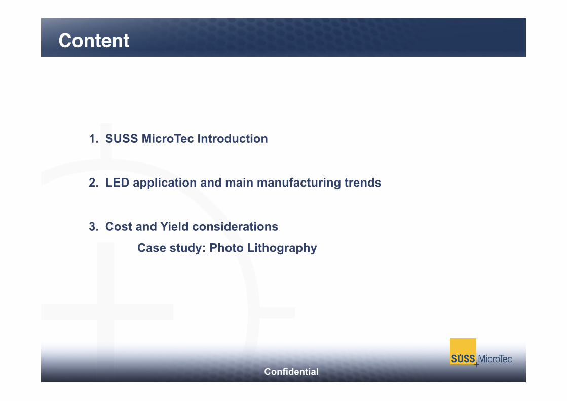
Content"
1. SUSS MicroTec Introduction
2. LED application and main manufacturing trends
3. Cost and Yield considerations
Case study: Photo Lithography

Confidential 3
SUSS MicroTec: At a Glance "
At a Glance Ê Founded 1949 by Karl Süss in Munich Ê Went public in 1999 (listed in Deutsche
Börse AG’s Prime Standard) Ê Revenue of the SUSS MicroTec group in
2010: ~140 Mil. Ê Global footprint with more than 8,000
systems installed worldwide
Ê SUSS MicroTec is one of the worldwide leading suppliers of equipment and process solutions for microstructuring in semiconductor and related industries
Ê Our focus lies on growth markets such as 3D Integration/Advanced Packaging, MEMS, III-V Semicompound/LEDs
1949 – 2009: Sixty Years of Engineering Spirit

4
Eq
uip
men
t &
Pro
cess
In
no
vati
on
s
Nano Imprinting Substrate conformal imprint
lithography for nm scale production of photonic crystals
Lens molding and replication
Full wafer scale nano imprinting Photonic Crystal Structures etched in Si-Wafer Ø 250 nm
Permanent Wafer Bonding Eutectic bonding (i.e. AuSn) Diffusion bonding (i.e. Au-Au)
Multi wafer bond tooling High throughout bonding process through multi wafer processing
Lithography Coating, exposure and developing
solutions for all relevant litho layer
HB LED top contacts [Exposed on a MA100e Gen2, Coat/Dev on SUSS Gamma 2010]
Thin Wafer Handling Supported temporary wafer bonding
processes: 3M, Brewer Science, TMAT
Temporary wafer bonding Temporary carrier technology to support manufacturing of thin-film LEDs with LLO
MA200Compact Mask Aligner
Gamma Coater/Developer
SB6/8e Wafer Bonder
SUSS Solutions for HB LED Manufacturing"

Content"
1. SUSS MicroTec Introduction
2. LED application and main manufacturing trends
3. Cost and Yield considerations
Case study: Photo Lithography
6
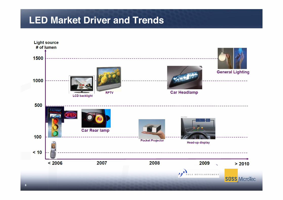
LED Market Driver and Trends"

7
Lets go for General Lighting – so what?"
Ê Device requirements to enter the market:
High Lifetime High Output
+
Low Costs
@
• Chip design optimization
• New materials
• Light efficiency improvements (PSS, PhC, etc.)
• Wafer size transition
• Higher productivity
• Wafer Level Packaging
Manufacturing Trends:

8
Lumen per Dollar Gap"
60W 800lm
Actual cost level: 300lm/$
Cost target for general lighting: 500lm/$
Source: Epistar
Incandescent Light Bulb LED Light Bulb

9
HB LED Device Structures and Trends"
Sapphire
n-GaN
n-pad
p-pad
Conventional LED device with patterend sapphire substrate (PSS) (essentially all LED chip makers)
n-GaN
n-pad
Thin-film vertical LED device with n-GaN texturing with substrate removal (Osram, Lumileds, Semileds, Cree, Luminus)
Conductor / Metall
+ Relatively inexpensive
- Up to 30% active surface lost to the Mesa
- Transparent or small contact needed on the p-side
- Current crowding due to poor conductivity of n-GaN increase total resistance
- Complexity and Cost
+ Good thermal properties
+ Larger active area (no MESA)
+ n-GaN can be thinned down to bring active layer close to the surface and improve light extraction (surface emitter)
+ Lower resistance
10
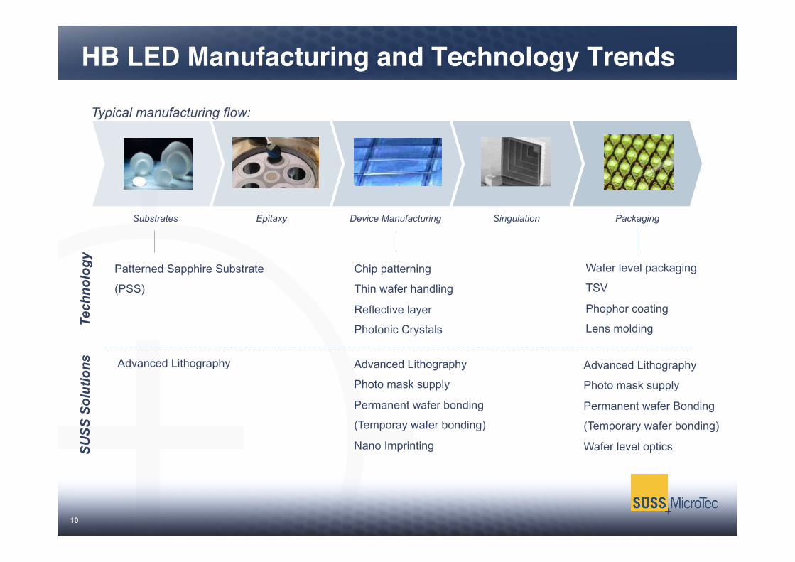
HB LED Manufacturing and Technology Trends"Te
chno
logy
SU
SS S
olut
ions
Substrates Epitaxy Device Manufacturing Singulation Packaging
Patterned Sapphire Substrate
(PSS)
Advanced Lithography
Chip patterning
Thin wafer handling
Reflective layer
Photonic Crystals
Advanced Lithography
Photo mask supply
Permanent wafer bonding
(Temporay wafer bonding)
Nano Imprinting
Wafer level packaging
TSV
Phophor coating
Lens molding
Advanced Lithography
Photo mask supply
Permanent wafer Bonding
(Temporary wafer bonding)
Wafer level optics
Typical manufacturing flow:

11
General HB LED Equipment Trends"
Ê Large wafer size support: 2” and 4” substrates are state of the art, first moves into 6”, firm plans for 200mm
Ê Cost of Ownership improvements: increase throughput multi-wafer processing higher yield lower CapEx
SUSS multi wafer bonding solution
Content"
1. SUSS MicroTec Introduction
2. LED application and main manufacturing trends
3. Cost and Yield considerations
Case study: Photo Lithography

13
Photo Lithography for HB LED manufacturing"
Ê Todays LED have up to seven lithography layers: General layers:
MESA etch, passivation N contact (lift-off) P contact (lift-off)
Additional lithography layers: Anti-current crowding Surface texturing (not always litho) Light guiding Bond / Bump layer patterning
Source: Epistar
14
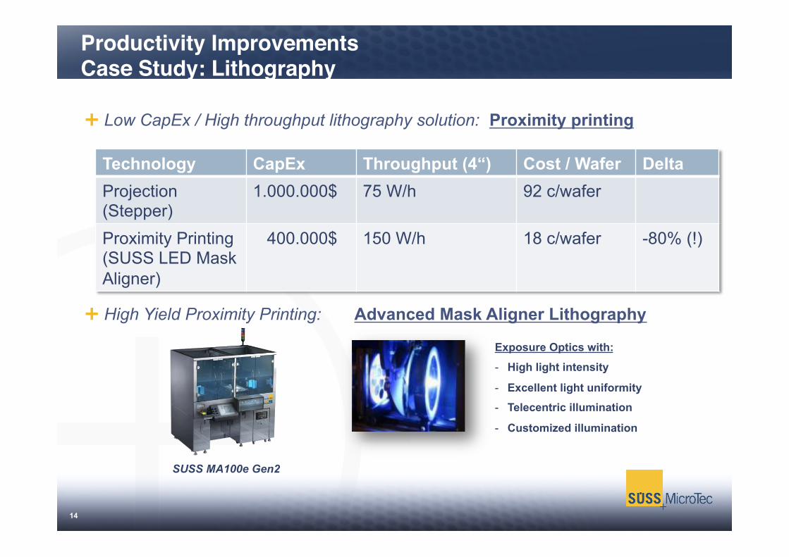
Productivity Improvements Case Study: Lithography"
Ê Low CapEx / High throughput lithography solution: Proximity printing
Ê High Yield Proximity Printing: Advanced Mask Aligner Lithography
Technology CapEx Throughput (4“) Cost / Wafer Delta Projection (Stepper)
1.000.000$ 75 W/h 92 c/wafer
Proximity Printing (SUSS LED Mask Aligner)
400.000$ 150 W/h 18 c/wafer -80% (!)
Exposure Optics with:
- High light intensity
- Excellent light uniformity
- Telecentric illumination
- Customized illumination
SUSS MA100e Gen2

Micro-Optics in Front-End Lithography"
15 ASML, Nikon, Canon
Micro-Optics is Key Enabling Technology in Front-End Lithography
Diffractive Optical Elements (DOE) MEMS Mirror Arrays (FlexRay™)
Customized Illumination
Excimer Laser (193nm)"Laser Beam Shaping "
Laser Beam Homogenizing"
Customized Illumination"Pupil Shaping (DOE)"
Now: FlexRay™ "programmable illumination
technology from ASML"
Microlens Köhler Homogenizer

Micro Optics
Illumination Filter Plate +
Macroscopic lenses in a fixed configuration:
Micro lens array coupled with a seperated filter plate:
Frontend Technology in SUSS Mask Aligner!

LED Yield Enhancements with Exposure Optics Tuning"
17
IFP-HR „High Resolution“
IFP-LGO „Large Gap“ IFP- „Talbot“
Equi
pmen
t Set
up
3D TSV lithography Talbot lithography (<5µm in 100µm gap) 2.5µm L/S in proximity printing (20µm)
Proc
ess
Res
ult
HB
LED
App
licat
ion

Summary"
1. Continued cost and light efficiency improvements are key enabler to enter the general lighting market place for LED
2. Photolithography is a significant cost contributor
3. New SUSS MicroTec technologies in proximity printing enable high yield and low resolution lithography on a cost effective equipment platform

Thank You!!