
Magnetodynamics of Pseudo-Spin-Valves
97
PH.D. THESIS DEPARTMENT OF PHYSICS Magnetodynamics of Pseudo-Spin-Valves Investigated Using Coplanar Wave Guide and Spin-torque Ferromagnetic Resonance Techniques Masoumeh Fazlali
Transcript of Magnetodynamics of Pseudo-Spin-Valves

Ph.D. thesis PH.D. THESIS
ISBN 978-91-629-0226-1 (PRINTED)ISBN 978-91-629-0225-4 (PDF)
Magnetodynam
ics of Pseudo-Spin-Valves | M
asoumeh Fazlali 2017
DEPARTMENT OF PHYSICS
Magnetodynamics of Pseudo-Spin-Valves
Investigated Using Coplanar Wave Guide and Spin-torque Ferromagnetic Resonance Techniques
Masoumeh Fazlali

Magnetodynamics of pseudo-spin-valves investigatedusing coplanar wave guide and spin-torque
ferromagnetic resonance techniques
Coupled and uncoupled trilayers, coincidence point resonance,and the high Q-factor peak at the resonance of coupled layers
Masoumeh Fazlali
Thesis for the degree ofDoctor of Philosophy in Natural Science, specializing in Physics
June 2017
‘Our job in physics is to see things simply, to understand a great many complicatedphenomena in a unified way, in terms of a few simple principles.’ Steven Weinberg
© Masoumeh Fazlali, 2017ISBN: 978-91-629-0226-1(printed)ISBN: 978-91-629-0225-4 (pdf)
Printed by Kompendiet, Gothenburg, 2017

Abstract
Nanocontacts (NCs) on magnetic multilayers are well-known in the implementation of spintorque oscillators, due to their frequency tunabilities that range from tens of GHz forspin-wave bullets and droplet-based oscillators to deeply sub-GHz bands for vortex-basedoscillators. Moreover, they can generate a wide range of highly nonlinear localized andpropagating SW modes for use in magnonics. However, I have found that most studieshave focused on the application point of view, and there are large unexplored areas in thefundamental physics of these structures.
This thesis focuses on exploring the magnetization dynamics of NCs on Co/Cu/Pypseudo-spin-valves (pSV) using the spin torque ferromagnetic resonance technique (ST-FMR) and the broadband conventional FMR technique. The thesis is thematically dividedinto two parts.
In the first part, which includes two papers, I utilize the ST-FMR technique to exciteand detect spin-wave resonance (SWR) spectra in tangentially magnetized NCs.
i) First, the origin of the magnetodynamics of the detected spectra is explored. I findthat the NC diameter sets the mean wavevector of the exchange-dominated spin wave, ingood agreement with the dispersion relation. The micromagnetic simulations suggest thatthe rf Oersted field in the vicinity of the NC plays the dominant role in generating thespectra observed.
ii) This work is followed by another work that involves tuning the exchange-dominatedspin wave using lateral current spread. To this end, different thicknesses of the Cu bottomlayer are used to control the lateral current spread.
In the second part, which includes three manuscripts, I explore the coupling betweentwo ferromagnetic layers through different thickness of Cu interlayers.
i) First, I study the nature of coupling in tangentially magnetized blanket trilayerCo/Cu/Py with different thickness of Cu of 0–40 Å by using broadband conventional fer-romagnetic resonance. I observe the oscillatory behavior of the exchange constant versusthe interlayer thickness, showing an RKKY type of interaction, although the exchangeconstant (J) is always positive. Three different regimes corresponding to alloy-like cou-pling (tCu ≤ 5A), strong FM coupling (the acoustic–optic regime, tCu = 7.5, 8.1, and16.2), and weak FM coupling (overall FM ordering, Cu ≥ 8.8) is found. Furthermore,the experimental results show a saturated field, especially in the Co shift to higher valuesin samples with stronger interlayer exchange coupling (IEC). Finally, in the case of thesamples corresponding to the collective regime, there is a critical field below which just

one acoustic mode exists. This mode below the critical field shows very low linewidth,compared to single-layer or alloy-like regime samples. These results demonstrate that, byusing the strength of the IEC, it is possible to engineer a cut-off frequency in magnetictrilayers, below which the spin pumping is turned off.
ii) Second, knowing the fact that Co and NiFe have very different Larmor frequencies inthe in-plane applied field (except very low f–H conditions), their f–H dependencies changeat higher angles of the applied field. I focus on the collective dynamics of the FM/N/FMsystem, when the FMR frequencies of the separate layers form a crosspoint (CP) at aparticular value of the applied magnetic field, and are substantially different otherwise.One of the CPs takes place when the applied field makes an 8 degree angle normal to thefilm at H = 11800 Oe, f = 13 GHz. Here again, I observe substantially different types offield spectra as a function of Cu thickness, but the borders of regimes are shifted. Whenthe Cu thickness is t < 8.5 Å, the trilayer structure has only one mode, that of the alloy-like behavior. For t = 8.8 and 16.6 Å, the structure shows the collective dynamics of bothlayers, which modify the FMR frequencies in the whole range of the applied field. For theintermediate value of t = 10 Å and the large values of t = 20 and t = 40 Å, the Co and NiFelayers demonstrate individual dynamics with low coupling. Such a periodical dependenceof the coupling strength on the spacer thickness confirms the previous work’s conclusionon the strong RKKY interlayer interaction. However, the shift of the regime borders for atypical sample in the two studies shows how the exchange coupling (J) relies on the anglebetween the magnetization of the two layers and, as a result, on the direction of the appliedfield. In the case of strong coupling (t = 8.8, t = 16.6 Å), a broad bandgap (> 1 GHz) isformed at the field spectra CP. At lower values of the applied field, the acoustic and opticalmodes have a strong blue frequency shift as compared to the uncoupled trilayer structure.This shift is especially large at H = 0 for the optical mode (∼ 4 GHz).
iii) Third, I studied the NC device with a trilayer pseudo-spin-valve with two differentinterlayer thicknesses (tCu = 20 Å and tCu = 80 Å) at the same field angle used in theprevious work, θ = 82◦. The aim of this work is to study the weakly coupled regime(tCu = 20 Å) and to compare it with the almost uncoupled regime (tCu = 80 Å) in thevicinity of the CP. Surprisingly, it is observed that sharp (high Q-factor) modes appear inthe vicinity of the CP in the weakly coupled regime. It seems that the coupling of FMlayers near the CP point tends to suppress all the spectra, except over a very small rangeof f–H, which leads to these sharp peaks. One possible explanation for this phenomenonis the Slonczewski mode nucleated by the spin pumping from Co to Py layer.

Dedication
This dissertation is dedicated to my loving parents, who showed me the most basic rule ofthe world, beyond all sciences: ‘The foundation of the universe is love.’


Acknowledgments
First and foremost, I am deeply grateful to my advisor, Professor Johan Åkerman. Beinga member of the Applied Spintronics group has been a milestone in my career that hasled me to explore my professional capabilities. Professor Åkerman’s expertise, generousscientific expenditure, and management of such a large group made it possible for me tofocus on the topics that interested me. In addition to his scientific knowledge, I have learnedfrom him how to work efficiently and systematically, and how to bring ideas efficiently topublication. I have learned from him how to keep up with the latest software, techniques,and technologies, so as to increase the value of the work, and how to stay up to date byattending conferences and daily literature reviews.
I appreciate my coadvisor, Dr. Martina Ahlberg, for all her support and collaborativeapproach. She was my mentor during the extremely busy final year of my PHD studies,where she worked with me on the analysis of data, and responded with endless patienceto my questions. I would also like to thank Dr. Randy K. Dumas for helping me to learnmeasurement techniques, running a fruitful course on applied spintronics, and as the seniorauthor who helped me write my first paper.
My sincere thanks go to Professor Pranaba Muduli at the Indian Institute of Technologyfor his kind support in solving equipment software issues during his annual visit at GU.I am also deeply grateful to Professor Mattias Goksör, the current head of the PhysicsDepartment at GU, for leading a great department with the strong support of studentsin every way. Special thanks are due to Professor Jonas Fransson at Uppsala University,regarding fruitful discussions for the last section of my thesis.
I would like to express my sincere gratitude to my collaborators in Professor PeterSvedlindh’s group for the pleasure of contribution in their excellent publications. A bigthanks also goes to Dr. Philipp Dürrenfeld for his endless support in the beginning, espe-cially in training me in nanofabrication, Dr. Ezio Iacocca, Dr. Roman Khymyn, and Dr.Mykola Dvornik for their fruitful discussions, and special thanks to Mykola Dvornik forhis simulation work on my first manuscript.
I should also thank Maria Siirak, Clara Wilow Sundh and Bea Augustsson for all oftheir administrative support during the four years of my PhD. Thank you so much for yourexcellent work!
Turning into my wonderful colleagues and friends in our group, I appreciate M. Balinsky,M. Haidar, A. Awad, M. Ranjbar, S.R. Etesami, H. Fulara, M. Zahedinejad, A. Hushang,J. Yue, Y. Yin, Sh. Muralidhar, S. Chung, A. Banuazizi, H. Mazraati, and all the Applied

Spintronics group members who have assisted me over these years.Finally, I would like to thank my father and two brothers, Mohammad and Reza.
Without their love and support over the years, none of this would have been possible.They have been always there for me and I am thankful for everything they have helpedme to achieve.

Publications
List of manuscripts and papers included in this thesis:
I M. Fazlali, M. Dvornik, E. Iacocca, P. Dürrenfeld, M. Haidar, J. Åkerman,and R. K. Dumas,“Homodyne-detected ferromagnetic resonance of in-plane magnetized nanocon-tacts: Composite spin-wave resonances and their excitation mechanism”,Physical Review B 93(2016), 134427.
II M. Fazlali, S. A. H. Banuazizi, M. Dvornik, M. Ahlberg, S. R. Sani, S. M.Mohseni, and J. Åkerman“Tuning exchange-dominated spin-waves using lateral current spread in nano-contact spin-torque nano-oscillators”,manuscript in preparation for Applied Physics Letters.
III M. Fazlali, M. Ahlberg, M. Dvornik, and J. Åkerman“Tunable spin pumping in exchange coupled magnetic trilayers”,manuscript in preparation for Physical Review Letters.
IV M. Fazlali, M. Ahlberg, R. Khymyn, and J. Åkerman“From individual to collective behavior in the multilayered magnetic structurein the vicinity of resonance coincidence point. Broadband FMR measurementsof the Co/Cu/Py trilayers”manuscript in preparation for Physical Review B.
V M. Fazlali, M. Ahlberg, M. Dvornik, and J. Åkerman“Effect of the microwave current on resonances of coupled Py/Cu/Co trilayersin oblique magnetic fields”,manuscript in preparation for Nature communication.
List of papers which I have contributed to, but are not included in this thesis:
VI A. Houshang, M. Fazlali, S. R. Sani, P. Dürrenfeld, E. Iacocca, J. Åkerman,and R. K. Dumas“Effect of sample fatigue on the synchronization behaviour on multiple nanocon-tact spin torque oscillator” ,IEEE Magnetics Letters, 5 (2014), 3000404.

VII A. Kumar, S. Akansel, H. Stopfel, M. Fazlali, J. Åkerman, R. Brucas, and P.Svedlindh“Spin transfer torque ferromagnetic resonance induced spin pumping in theFe/Pd bilayer system”,Physical Review B 95 (2017), 064406.

Declaration
This thesis is a presentation of my original research work. It is the result of cooperativeefforts, and I am grateful for the contributions and endless support of my colleagues. Thework was performed under the guidance of Professor Johan Åkerman, at the Departmentof Physics, University of Gothenburg, Sweden. The contributions of the author (MF) tothe appended papers are as follows:
Paper I : MF performed the measurement, contributed to the analytical approachwith MD and wrote the first manuscript (except simulation and discussion sections).
Paper II : MF performed the measurement, designed the analytical approach, andwrote the first manuscript.
Paper III : MF fabricated the samples, performed the measurement, and contributedto the analysis with MA.
Paper IV : MF fabricated the samples, performed the measurement, contributed tothe analysis with MA and RK, and wrote the first manuscript.
Paper V : MF fabricated the devices, performed the measurement, set meetings withJF regarding Fano discussions, contributed to the analysis with MA, MD, and wrote thefirst manuscript.
Paper VI : MF performed ST-FMR measurements and ST-FMR analysis.Paper VII : MF contributed to the fabrication of devices and reviewed the paper.
Masoumeh Fazlali

Contents
1 Basics 11.1 Spin waves . . . . . . . . . . . . . . . . . . . . . . . . . . . . . . . . . . . . 1
1.1.1 The concept of spin waves . . . . . . . . . . . . . . . . . . . . . . . 11.1.2 Spin waves in infinite media (without boundary conditions) . . . . . 11.1.3 Types of spin waves in ferromagnetic films (with boundary conditions) 31.1.4 Magnetostatic spin waves . . . . . . . . . . . . . . . . . . . . . . . 31.1.5 Exchange spin waves . . . . . . . . . . . . . . . . . . . . . . . . . . 51.1.6 Slonczewski propagating spin-wave . . . . . . . . . . . . . . . . . . 71.1.7 Techniques for exciting spin waves . . . . . . . . . . . . . . . . . . . 7
1.2 Coupling between two ferromagnet layers in trilayer spin valves . . . . . . 81.2.1 Main contributions to the magnetic Hamiltonian . . . . . . . . . . . 81.2.2 Interlayer exchange coupling (IEC) . . . . . . . . . . . . . . . . . . 81.2.3 Spin pumping . . . . . . . . . . . . . . . . . . . . . . . . . . . . . 91.2.4 Models for fitting FMR modes of a trilayer system . . . . . . . . . 91.2.5 Anticrossing at the resonance coincidence point in collective regime 121.2.6 Fano resonance . . . . . . . . . . . . . . . . . . . . . . . . . . . . . 121.2.7 A classical analogy for Fano resonance: two coupled oscillators . . . 13
2 Methods: fabrication and measurement 152.1 Device fabrication . . . . . . . . . . . . . . . . . . . . . . . . . . . . . . . . 16
2.1.1 Sample deposition by magnetron sputtering . . . . . . . . . . . . . 162.1.2 Mark alignment and prepatterning of mesa and electrical pads by
photolithography . . . . . . . . . . . . . . . . . . . . . . . . . . . . 172.1.3 Fabrication of mesas through ion beam milling . . . . . . . . . . . . 192.1.4 Prepattern nanogap by E-beam lithography . . . . . . . . . . . . . 192.1.5 Etching of exposed e-beam resist areas through reactive ion etching 20
2.2 Characterization of the trilayer stack and NC-STOs . . . . . . . . . . . . . 202.2.1 Giant magnetic resistance . . . . . . . . . . . . . . . . . . . . . . . 202.2.2 Ferromagnetic resonance technique . . . . . . . . . . . . . . . . . . 212.2.3 Spin-torque ferromagnetic resonance technique . . . . . . . . . . . . 24

3 Spin waves in in-plane magnetized NC-STOs 283.1 Homodyne-detected ferromagnetic resonance of in-plane magnetized nanocon-
tacts . . . . . . . . . . . . . . . . . . . . . . . . . . . . . . . . . . . . . . . 293.1.1 The peak asymmetry in ST-FMR spectra of Py in the NC-geometry
literature . . . . . . . . . . . . . . . . . . . . . . . . . . . . . . . . 293.1.2 Study of ST-FMR spectra of Py with different NC diameters . . . . 293.1.3 Fit the Py spectra with two Lorentzian functions . . . . . . . . . . 293.1.4 Fit frequency-field dependency of satellite peak with dispersion relation 323.1.5 Micromagnetic simulations . . . . . . . . . . . . . . . . . . . . . . . 323.1.6 Anisotropic nature of spin waves propagation . . . . . . . . . . . . 343.1.7 Dependence of coexistence band of magnetostatic and exchange-
dominated SWs on the thickness of FM layer . . . . . . . . . . . . . 343.1.8 Oersted field: the main origin of magnetodynamics . . . . . . . . . 353.1.9 The place of cut-off wave vector in SW bands . . . . . . . . . . . . 373.1.10 NC diameter dependence of the FMR and SWR inhomogeneous
broadenings . . . . . . . . . . . . . . . . . . . . . . . . . . . . . . . 373.1.11 Conclusions . . . . . . . . . . . . . . . . . . . . . . . . . . . . . . . 38
3.2 Tuning exchange-dominated spin-waves using lateral current spread in NC-STO . . . . . . . . . . . . . . . . . . . . . . . . . . . . . . . . . . . . . . . 393.2.1 Another method for changing the distribution of Oersted field . . . 393.2.2 Study of spin wave spectra of Py with different thicknesses of bottom
electrode . . . . . . . . . . . . . . . . . . . . . . . . . . . . . . . . . 393.2.3 Experimental results . . . . . . . . . . . . . . . . . . . . . . . . . . 393.2.4 COMSOL simulation . . . . . . . . . . . . . . . . . . . . . . . . . . 403.2.5 Conclusions . . . . . . . . . . . . . . . . . . . . . . . . . . . . . . . 42
4 Exchange coupling between two FM layers 434.1 Tunable spin pumping in exchange-coupled magnetic trilayers . . . . . . . 45
4.1.1 Fit of individual layers with Kittel equation . . . . . . . . . . . . . 454.1.2 Fit of multilayers with free energy numerical model . . . . . . . . . 454.1.3 The positive oscillatory behaviour of interlayer coupling . . . . . . . 464.1.4 The effect of IEC on linewidth of low frequency resonance modes . 474.1.5 Study amplitude of the modes - transition to collective regime . . . 484.1.6 Conclusion . . . . . . . . . . . . . . . . . . . . . . . . . . . . . . . . 49
4.2 From individual to collective behavior in multilayered magnetic structuresin the vicinity of the resonance coincidence point . . . . . . . . . . . . . . 504.2.1 Experiment and numerical model of Kittel equation for fit in an
oblique field . . . . . . . . . . . . . . . . . . . . . . . . . . . . . . . 504.2.2 Numerical model for exchange coupled multilayers . . . . . . . . . . 514.2.3 Three distinctly different regimes . . . . . . . . . . . . . . . . . . . 514.2.4 Field-frequency dependency characteristics of each regime . . . . . 524.2.5 Linewidth-frequency dependency characteristics of each regime . . . 554.2.6 Amplitude-frequency dependency characteristics of each regime . . 56

4.2.7 Conclusion . . . . . . . . . . . . . . . . . . . . . . . . . . . . . . . . 574.3 Effect of microwave current on resonances of coupled Py/Cu/Co trilayers in
oblique magnetic fields . . . . . . . . . . . . . . . . . . . . . . . . . . . . . 594.3.1 Sample layout and experimental setup . . . . . . . . . . . . . . . . 594.3.2 Characterization of samples in in-plane field configuration . . . . . 594.3.3 Characterization of samples in out of plane angle of the field . . . . 604.3.4 Discussion . . . . . . . . . . . . . . . . . . . . . . . . . . . . . . . . 624.3.5 Conclusion . . . . . . . . . . . . . . . . . . . . . . . . . . . . . . . . 64
5 Conclusions and future works 66

Chapter 1
Basics
1.1 Spin waves
1.1.1 The concept of spin waves
In 1930, the concept of spin waves as elementary excitations that occur in ordered mag-netic materials was introduced by Bloch [1]. He was the first to present the idea that thedynamic excitations of the spin system of magnetic crystals had the character of the col-lective precession of the individual spins, which can be represented as a propagating wave.When the quantum-mechanical nature of the spins is taken into account, the correspondingquasiparticles that arise from the quantization of the spin waves are called magnons.
In fact, various alternative approaches to spin wave theory can be followed. Thesemathematical frameworks include semiclassical approaches, such as that due to Heller andKramers [2] (Fig. 1-1) and quantum-mechanical approaches. The semiclassical approachis particularly helpful in gaining physical interpretations.
Spin waves at low temperatures behave, to a good approximation, as noninteracting el-ementary excitations with boson-like characteristics. However, it should be noted that spinwaves are not exact normal modes of the system, and this leads to an interaction betweenthem and also to other nonlinear effects [5]. The path of the discovery of experimentalevidence for spin waves can be found, for example, in Refs. [3, 4].
1.1.2 Spin waves in infinite media (without boundary conditions)
Maxwell’s equations for magnetoquasistatics reduce to
∇× h = 0 (1.1)
∇.b = 0
∇× e = iωb.
For a magnetized film, we haveb = µ.h (1.2)
1

Figure 1.1: Semiclassical representation of a spin wave in a ferromagnet: (a) ground statewith magnetization vectors parallel: M(t = 0) = M0
#»
k ; (b) perspective view of a spin wave ofprecessing spin vectors: M(t) = Mz
#»
k +Mreiωt #»r ; (c) top view: the oscillating component of the
magnetization vector, Mreiωt #»r .
µ = µ0(I + χ),
where µ is the permeability tensor.
χ =
[χ iχa
−iχa χ
](1.3)
χ =ωMωH
ω2H − ω2
, χa =ωMω
ω2H − ω2
, ωH = γµ0H0, ωM = γµ0M0.
Assuming the bias field (H0) lies along the z-direction, combining the equations leadsto
(1 + χ)
[∂2A(r)
∂x2+
∂2A(r)
∂y2
]+
∂2A(r)
∂z2= 0. (1.4)
Equation (1.4) is called Walker’s equation and is the basic equation for magnetostaticmodes in homogeneous media [5]. It is well-known that any excitation, such as spin waves,must satisfy the symmetry requirements in accordance with Bloch’s Theorem [6], whichstates that the variable A(r) describing the spin-wave amplitude must have the generalform
A(r) = exp(ik.r) Uk(r). (1.5)
2

Here, k is a wavevector in the Brillouin zone corresponding to the reciprocal lattice ofthe crystal, and Uk(r) is a periodic function of the potential of the crystal lattice. Theoverall phase vector exp(ik.r) gives a plane-wave variation to A(r). For a spin wave, A(r) isthe appropriate component of spin of the magnetization. The spin-wave energy is denotedby hω(k) where ω(k) is the excitation frequency [7].
If the propagation angle with respect to the z-axis (also the direction of the DC biasfield) is θ, then putting (1.5) into Equation (1.4) gives:
χ sin2 θ = 1. (1.6)
This can be expressed explicitly in terms of the frequency using Equation (1.3) for χ:
ω =[ωH(ωH + ωM sin2 θ)
]1/2. (1.7)
This shows the independence of k from the magnitude: that is, waves at this frequency canhave any wavelength. This happens because we did not assume any boundary conditions.In real experiments on spin waves, samples of finite size are always used. Taking intoaccount the boundary conditions on the film surfaces leads to changes in the spin-wavespectrum: first there is a discrete spin-wave spectrum consisting of separate dispersionbranches corresponding to spin waves with different distributions of variable magnetizationacross the film thickness. Second, the spin-wave eigenfrequencies depend on the magnitudeof the wavevector.
1.1.3 Types of spin waves in ferromagnetic films (with boundaryconditions)
The magnitude of the wavevector k of a spin wave identifies its properties. The dipole–dipole interaction plays a fundamental role in the propagation of relatively long-wavelengthspin waves with wavenumbers |k| ≤ 107 m−1, where the wavelength may be comparable tothe characteristic size of the ferromagnetic sample. Such waves are customarily referred toas magnetostatic spin waves [7]. For short-wavelength spin waves (with |k| > 108 m−1),the exchange interaction plays a fundamental role. The exchange region includes most ofthe Brillouin zone (a zone-boundary wavevector has a magnitude of about 1010 m−1). Inorder to emphasize this distinction, we will refer to such waves as exchange spin waves.Finally, there is an intermediate region, referred to as the dipole-exchange region, typicallycorresponding to 108 m−1 > |k| > 107 m−1, in which the dipole and exchange termsare comparable. At very small values of |k|, the full form of Maxwell’s equations shouldbe used; this region is called the electromagnetic region. Table 1.1 summarizes differentregions of spin waves.
1.1.4 Magnetostatic spin waves
Magnetostatic spin waves (MSWs) are anisotropic due to the anisotropic nature of dipolarinteraction. MSWs in a normally magnetized film are called forward-volume magnetostatic
3

Region Wavevector rangeExchange region |k| > 108 m−1
Dipole-exchange region 108 m−1 > |k| > 107 m−1
Magnetostatic region 107 cm−1 > |k| > 3× 10³ m−1
Electromagnetic region |k| < 3× 10³ m−1
Table 1.1: Different regions of spin-wave excitations in terms of the magnitude |k| of theirwavevector. The numbers are approximate for ferromagnetic materials. For comparison, a Bril-louin zone boundary wavevector is approximately of magnitude 1010 m−1 [8].
waves (FVMSWs). MSWs in an in-plane magnetized magnetic film are classified in twoways, depending on the angle between k and the applied field (H). Waves propagatingalong the applied field are called backward-volume magnetostatic waves (BVMSWs), whilewaves propagating transverse to the applied field are called magnetostatic surface waves(MSSWs, also known as Damon–Eshbach waves) [9].
The dispersion relation for FVMSWs in a normally magnetized film is
ω2 = ωH
[ωH + ωM
(1− 1− e−kd
kd
)]. (1.8)
The phase and group velocities are both in the same direction. Waves with this character-istic are called forward waves. In addition, the wave amplitude is distributed sinusoidallythrough the volume of the film. Because of these two characteristics, these are calledmagnetostatic forward-volume spin waves (Fig. 1.2).
The dispersion relation for BVMSWs in a tangentially magnetized film is:
ω2 = ωH
[ωH + ωM
(1− e−kd
kd
)]. (1.9)
The phase and group velocities here point in opposite directions. A wave with this propertyis called a backward wave; the wave amplitude is then distributed sinusoidally through thevolume of the film. The term magnetostatic backward-volume wave follows from these twocharacteristics (Fig. 1.2). The dispersion relation for MSSWs in a tangentially magnetizedfilm is:
ω2 = ωH(ωH + ωM) +ω2M
4
[1− e−2kd
]. (1.10)
The phase and group velocities point in the same direction, and thus this mode is a forwardwave. The wave amplitude is not distributed periodically through the film thickness, butinstead decays exponentially from the surfaces of the film. Because of this last observation,these modes are called magnetostatic surface waves (Fig. 1.2). The dispersion relation of allthree types of magnetostatic waves for the sample NiFe with t = 100 nm are demonstratedin Figure 1.2.
4

Figure 1.2: (a) Dispersion relation of different types of spin waves for FMR resonance conditionat f = 18 GHz in NiFe film with a thickness of t = 100 nm. The solid and dashed lines respectivelyshow the dispersion relation, with and without the exchange term. (b) Dynamic magnetizationprofile of modes.
1.1.5 Exchange spin waves
In the presence of exchange, h is obtained from m using the matrix differential Aop:
h = Aop.m, (1.11)
whereAop =
1
ωM
[ωH − ωMλex∇2 iω
−iω ωH − ωMλex∇2
].
For uniform plane wave propagation, A(r) = exp(ik.r) Uk(r), the operator ∇2 can bereplaced by the factor k2. Since the exchange term ωMλexk
2 appears everywhere with ωH ,it follows that the effects of exchange can be added to the previous magnetostatic plane
5

Figure 1.3: Comparison between dispersion relations of in-plane magnetized NiFe samples withd = 100 nm and d = 4.5 nm shown by dashed lines and solid lines, respectively.
wave analysis by simply replacing ωH by ωH + ωMλexk2. Figure 1.2 (a) shows the effect
of adding the exchange term to the dispersion relation of all three types of magnetostaticspin wave.
Figure 1.3 shows the dispersion relations of tangentially magnetized NiFe film with twodifferent thickness. From this plot, it can be seen that for ultrathin films, the criticalwavevector that defines the borders between the magnetostatic regime and the exchangeregime goes to zero—i.e., the exchange interaction dominates the magnetodynamics intangentially magnetized ultrathin films. As a result, for ultrathin films, the dispersionrelations simply follow equation (1.12).
ω =
[ (ωSWR
H + ωM (λexk)2)× (
ωSWRH + ωM + ωM (λexk)
2) ]1/2 (1.12)
where λex =√
2A/µ0M2s and k are the exchange length and the spin wave resonance
(SWR) wavevector, respectively. Any physical confinement or quasiconfinement (D′) canlead to discrete values of k = nπ/D′, which for the first order approximates to k = π/D′.
The study of exchange spin waves is interesting both from the applications and funda-mental points of view. Along with elastic and magnetostatic waves, exchange spin wavesare “slow” waves—that is, their phases and group velocities are small compared to the veloc-ity of an electromagnetic wave (Table 1.1). This is why exchange spin waves are promisingcandidates for use in making small microwave engineering elements, similar to those thatuse surface acoustic waves and magnetostatic spin waves. On the other hand, the wave-length of exchange spin waves is comparable to that of sound and light waves; These spinwaves could thus be important objects and instruments for investigating the interactions
6

between waves of various types. The experimental study of exchange spin waves, whichstarted more than fifty years ago, involves the use of three basic experimental methods:the study of spin-wave resonance spectra in thin ferromagnetic films, the measurement offrequency and field dependencies of the threshold for parametric excitation of exchangespin waves, and the investigation of the scattering of light by thermal or parametricallyexcited magnons [7, 10].
1.1.6 Slonczewski propagating spin-wave
Types of spin waves, including magnetostatics and magnetodynamics, have been gener-ally discussed. In 1996, Slonczewski showed theoretically[11] and later confirmed exper-imentally [12, 13, 14] that a sufficiently large electric current passing through a trilayerferromagnetic/nonmagnetic/ferromagnetic (F/N/F) with noncollinear magnetizations cantransfer vector spin between the magnetic layers, exciting precession of the layer magneti-zations, and as a result stimulating the emission of propagating spin waves (exchange spinwaves). In 2007, Slavin et al.[15] showed in the case of nanocontact geometry, the directionof the external bias magnetic field and the variation in the magnetization angle can leadto a qualitative change in the nature of the excited spin wave modes.
In the case of a normally magnetized film, the frequency of the excited spin wave isalways larger than the frequency of the FMR mode of the free magnetic layer:
ω(k) = ωH + ωM (λexk)2 +Na2 (1.13)
where N is the coefficient of a nonlinear frequency shift and in this geometry is alwayspositive, N > 0; a is the amplitude of the excited spin wave mode. In the case of an in-plane magnetized nanocontact, the coefficient of the nonlinear frequency shift is negative,N < 0, and therefore has the opposite sign of the exchange term. This geometry can thussupport a strongly localized nonpropagating spin wave mode of a solitonic type.
1.1.7 Techniques for exciting spin waves
Initially, the first experimental evidence of spin waves came from the measurement of ther-modynamic properties [1]. Nowadays, however, there exist sensitive direct techniques tostudy magnetodynamics (both linear and nonlinear processes) involving spin-wave exci-tations. Spin waves are excited using the following techniques: via an rf Oersted fieldproduced by various kinds of antennas [16], by light scattering (ultrafast laser pulses) [17],by neutron scattering [4], through parametric amplification of SWs from thermal fluctua-tions [9], via magnetoelectric interactions [18], and by spin transfer torque (STT) [19].
7

1.2 Coupling between two ferromagnet layers in trilayerspin valves
1.2.1 Main contributions to the magnetic Hamiltonian
The energy of the magnetic system can be mainly expressed by the exchange energy andthe magnetic dipole–dipole energy and, in the case of an anisotropic system, anisotropyenergy. These three terms are expressed respectively as:
Eex =∑<i,j>
Ji,jSi.Sj (1.14)
Ed = (gµB)2∑<i,j>
(Si.Sj
r3i,j
3(Si.ri,j)(Sj.ri,j)
r5i,j
)(1.15)
Ea =∑<i>
K(SZi )
2. (1.16)
The exchange interaction is a short-range interaction, and in most cases it is sufficientto consider only nearest neighbor sites. Equation 1.13 shows the simplest form of the ex-change energy. Equation 1.14 shows the dipole–dipole interaction contribution to magneticenergy. There is a magnetic moment gµBSi corresponding to each spin Si. The dipole–dipole interaction is much smaller than the exchange interaction (2–3 orders of magnitudesmaller). However, for the magnetic dynamic properties (e.g., spin waves) at small enoughwavenumbers (long wavelengths), the effect of the dipole–dipole interaction becomes sig-nificant, as the dipole–dipole interaction is long range and the exchange interaction is shortrange.
There are other contributions to the Hamiltonian of a magnetic system, includinganisotropy. Anisotropy arises from the interaction of the magnetic moment of atoms withthe electric field of the crystal lattice. Equation 1.15 shows a simplified description of theanisotropy contribution in a uniaxial (noncubic) ferromagnet, where K is an anisotropyconstant [5].
1.2.2 Interlayer exchange coupling (IEC)
Trilayer FM/NM/FM systems have been the subject of many studies due to their ap-plications in magnetic recording devices and nonvolatile magnetic random memories [20].Variation of the intervening nonmagnetic interlayer tunes not only the strength of coupling,but also the type of coupling for ultrathin interlayer thicknesses. Bilinear coupling is one ofstrong models that fits the resonance condition of such systems. This coupling is describedas bilinear, since the relative surface coupling energy is proportional to the magnetizationproduct:
Ec = −Jmimi+1. (1.17)
8

Generally, bilinear coupling in spin-valve structures or MTJs results from the combinationof two contributions [21]:
RKKY interaction
The conduction-electron-mediated exchange coupling, which oscillates in sign as a functionof the thickness of the metallic spacer layer and which is closely related to the well-knownRKKY interaction [22] between magnetic impurities in a nonmagnetic host. This couplingwas first observed in 1986 [23].
Néel coupling
Dipolar magnetic coupling (also known as Néel coupling or ‘orange-peel’ coupling) is ferro-magnetic and arises from magnetostatic charges present at the interfaces and induced bysurface roughness. This model predicts an exponential increase in dipole coupling betweenthe magnetic layers with decreasing spacer thickness (Fig. 1.4).
Figure 1.4: Schematic representation of a trilayer with conformal sinusoidal interface roughnessinducing orange-peel FM coupling [21].
1.2.3 Spin pumping
While the static IEC is oscillating and short-ranged in nature, there also exists a dynamicand long-ranged coupling between magnetic layers, called spin pumping. The concept ofspin pumping describes how the leakage of angular momentum (spin current) from a pre-cessing magnetic film may be absorbed at the interface to another magnetic/nonmagneticlayer, which provides an additional damping term [24, 25, 26]. The dimensionless damp-ing coefficient is then given by α = α(0) + αsp, where α(0) is the intrinsic damping of theprecessing layer and αsp is the spin-pumping-induced term.
1.2.4 Models for fitting FMR modes of a trilayer system
The Kittel equation is well defined and widely used due to its simplicity, though it can onlybe used for single layers. In the case of multilayer systems, one approach is to considereach resonance mode individually and to use the Kittel equation by adding an exchange
9

field Hadd [27, 28] to the internal field due to coupling. However, we observed that thismethod not only gave quite poor fits, but the J ′ values determined independently fromHPy
add and HCoadd also differed significantly.
Improvements can be made if the heterogeneous nature of the structure is accountedfor, instead of focusing on one component at a time. For this purpose, complex numericalmodels are suggested to obtain the eigenmodes of the multilayer system. One of thesemodels is an approach where the relation between fr and Hr is derived from the freeenergy of the system, giving the following expression [29, 30, 31]:
aω4 + cω2 + eω = 0 (1.18)
where ω = 2πfr, and the coefficients a, c, and e contain the interlayer coupling, themagnetic properties, as well as the thickness of the magnetic layers.
Another model was suggested by Franco et al. in 2016 [32]. This was a simple modelfor the FMR of an exchange-interacting heterogeneous multilayer system that accountssimultaneously for all the resonance modes of the structure. Here we simplify the modelfor the trilayer structure (two FM layers), ignoring uniaxial anisotropy and cubic anisotropydue to the amorphous nature of both layers.
Figure 1.5: Cartesian coordinate system and notations for layer i [32].
Assuming that zi lies in the equilibrium direction of Mi, the magnetization can bewritten in the form of a static term (M (0)
i ) and the dynamic magnetization as mi, perpen-dicular to that. iωres/γ, where ωres = 2πfres and γ is the gyromagnetic ratio, is given bythe eigenvalues of the 4× 4 dynamic matrix Dm:
Dm = µ0
−Hy0,x0 −Hy0,y0 −Hy0,x1 −Hy0,y1
Hx0,x0 Hx0,y0 Hx0,x1 Hx0,y1
−Hy1,x0 −Hy1,y0 −Hy1,x1 −Hy1,y1
Hx1,x0 Hx1,y0 Hx1,x1 Hx1,y1
. (1.19)
10

The components Hαiβη of Dm are the dynamic fields linked to the second-order combi-nations of the dynamic components of the magnetizations. The internal dynamic fields foreach individual layer are given by:
HIxixi
= HCS(Mi, H)−M is(cos
2 θMi− sin2 θMi
)
HIyiyi
= HCS(Mi, H)−M is cos
2 θMi, (1.20)
where CS(A,B) ≡ cos θA cos θB +sin θA sin θB, and θA(B) is the angle that the vector A(B)forms with the normal of the layer zc. The first term in both equations stems from theZeeman energy, and the second term from the demagnetization field. H is the magnitudeof the applied field and M i
s is the saturation magnetization of layer i. To account for theinterlayer exchange coupling, the following fields need to be included:
HJxixi
= HJyiyi
=Jeff
µ0M isti
CS(Mi,Mj)
HJxixj
= − Jeff
µ0Mjs ti
SC(Mi,Mj)
HJyiyj
= − Jeff
µ0Mjs ti
, (1.21)
where SC(Mi,Mj) ≡ sin θMisin θMj
+ cos θMicos θMj
, and ti is the thickness of layer i.Jeff is the exchange interaction between FM layers and is positive for FM EC. The dynamicfields that compose the matrix Dm are calculated by adding the internal fields (1.15) andinterlayer EC contributions (1.16) for each layer, as given by
Hαiβη = HIαiβη
+HJαiβη
, (1.22)
where α and β are any contribution of x, y, and η is either i or j. The susceptibilitytensor can be obtained by using:
χ = D−1g MT , (1.23)
where
MT ≡
0 −M0s 0
M0s 0 −M1
s
0 M1s 0
and the matrix Dg is given by: Dg = iω
γW + Dm. ω is the angular frequency of the
microwave field, and the matrix W is given by:
W =
1 g0 0−g0 1 g10 −g1 0
,
with gi the Gilbert damping parameter of layer i.
11

By having dynamic susceptibility, the FMR resonance linewidth can be extracted bynumerically solving:
Im[χyy(ω,Hωres +∆Hω
lw)] =1
2Im[χyy(ω,H
ωres)], (1.24)
where µ0∆Hωlw is the field linewidth of the oscillation mode related to the resonance field
µ0Hωres and the frequency ω.
1.2.5 Anticrossing at the resonance coincidence point in collectiveregime
Exchange coupled magnetic layers exhibit collective dynamics and their ferromagnetic res-onance (FMR) spectra display two modes – acoustical and optical – corresponding toin-phase and out-of-phase precession, respectively. The model of Franco et al. for the caseof a perpendicular applied field in a CoFe/NiFe bilayer shows that the layers cross eachother at field µ0H ≈ 1.345T when Jeff = 0. By adding an FM EC at the interface, themodel predicts a frequency gap of ∆fg at the crossing point (CP), Figure 1.6(a). The FMacoustic and optic modes at weak fields follow the NiFe and CoFe respectively. This isbecause, for weak applied fields, the resonance frequency of the NiFe is lower than that ofCoFe. The opposite happens for strong fields after the CP. Thus, the modes switch theirrespective governing layers. It is at this transition from one governing layer to another thatthe gap appears. Figure 1.6 (b) shows the linewidth behavior of both acoustic and opticmodes in the vicinity of the crossing point. It shows that the evolution of the linewidth isthe same as the evolution of the frequency in Figure 1.6 (a). This confirms that the changein the governing layer strongly affects the frequency linewidth.
1.2.6 Fano resonance
Fano interference is a universal phenomenon, as the characteristics of the interference donot depend on the characteristics of the material. In spintronics, Fano resonance can beutilized in practice to implement quantum probes that provide important information onthe geometric configuration and internal potential fields of low-dimensional structures [33].Other potential applications of Fano resonance include new types of spintronics devices,such as Fano transistor [34] and Fano filters. In addition, from the basic science pointof view, there are a few wave phenomena that represent milestones in modern physics—such as Young’s interference in optics or Ahoronov–Bohm (AB) interference in quantummechanics. Undoubtedly, Fano interference phenomena are of this type [33].
If the coupling parameter q becomes very strong (q � 1), then the Fano profile reducesto a symmetric Breit–Wigner (BW) (or Lorentzian) lineshape [35]. It has been shown thatBW resonances arise due to the interference of two counterwaves in the same scatteringchannel. On the other hand, Fano resonance takes place due to wave interference indifferent channels.
12

Figure 1.6: Theoretical model of resonance condition of exchange-coupled CoFe/NiFe bilayerin perpendicular field. (a) Frequency vs. field of the acoustic and optic modes for both positiveand negative values of coupling (±0.5 mJ/m2), in comparison to the case where J = 0 mJ/m2.(b) Linewidth vs. field of the acoustic and optical FM modes of a NiFe/CoFe bilayer (J =+1mJ/m2) [32].
1.2.7 A classical analogy for Fano resonance: two coupled oscilla-tors
Considering a pair of harmonic oscillators coupled by a weak spring, this section reviews theequation of motion for the behavior of the forced oscillator. For two harmonic oscillatorswith coupling υ12, this can be written as:
x1 + γ1x1 + ω21x1 + υ12x2 = a1e
iωt (1.25)
x2 + γ2x2 + υ12x2 = 0,
where a1eiωt is the external force. The eigenmodes of such a system can be written as:
ω12 ≈ ω2
1 −υ212
ω22 − ω2
1
, ω22 ≈ ω2
2 +υ212
ω22 − ω2
1
. (1.26)
The steady-state solutions of this system are:
x1 = c1eiωt, x2 = c2e
iωt, (1.27)
where c1 and c2 are the amplitudes of the forced oscillator and the coupled oscillator isgiven by:
c1 =(ω2
2 − ω2 + iγ2ω)
(ω21 − ω2 + iγ1ω)(ω2
2 − ω2 + iγ2ω)− υ212
a1
13

c2 = − υ12(ω2
1 − ω2 + iγ1ω)(ω22 − ω2 + iγ2ω)− υ2
12
a1. (1.28)
The phases of the oscillations are defined by:
c1(ω) = |c1(ω)|e−iφ1(ω)
c1(ω) = |c1(ω)|e−iφ1(ω). (1.29)
The phase difference between the two oscillators is: φ2 − φ1 = π − θ, where the extraphase shift θ = arctan( γ2ω
ω22−ω2 ). The effective friction (γ2) for normal modes causes the
amplitude of the oscillators to be limited. The amplitude and phase of both oscillators asa function of the frequency of an external force are shown in Figure 1.7 [33].
Figure 1.7: Resonance amplitude and phase of a forced oscillator (a) and a coupled oscillator(b) in a harmonic coupled system. The frequency is in the unit of natural frequency ω1. Theamplitude has two peaks near the eigenfrequencies. Here, γ1 = 0.025; γ2 = 0; υ12 = 0.1 [33].
14

Chapter 2
Methods: fabrication and measurement
Nanocontacts (NC) on pseudo-spin-valves are particularly promising for high-frequencyspin-torque oscillators (NC-STOs) [36, 37, 38, 39, 40, 41, 42, 43, 44, 45, 46, 47, 48, 49,50, 51] and for the emerging field of ST-based magnonics, [52, 53, 9, 54, 55] (Section 4.3)where highly nonlinear auto-oscillatory modes are utilized for operation. I have performedfundamental research on this structure by using ferromagnetic resonance techniques (FMRand ST-FMR), as described in Chapters 3 and 4. In this chapter, I briefly go through thesteps of device fabrication and then explain the ferromagnetic resonance techniques usedfor the measurement of blanket samples and nanocontact devices.
15

2.1 Device fabricationThe fabrication of NC-STOs has previously been developed in the Applied Spintronicsgroup [43]. The stack of thin film layers is deposited by an AJA magnetron sputteringsystem on SiO2/Si substrate pieces (Fig. 2.1(a)). The mesa (the active area) and alignmentmarks are then prepatterned by photolithography and the mesa is defined by ion millingusing SIMS monitoring (Fig. 2.1(b)). Afterward, the process is followed by sputteringthe insulating layer, SiO2, on top of the sample (Fig. 2.1(c)). Then, by means of E-beam lithography (EBL), the nanogap is defined in the middle of the mesa flanked by twomicron-size gaps, followed by SiO2 reactive ion etching (RIE), (Fig. 2.1(d)). Finally, thefabrication of the NC-STO finished with the creation of electrical pads in a lift-off process(Fig. 2.1(e)). After finishing each step and before going on to the next, an optical/SEMinspection is performed to determine if the micro/nanofabrication process was clean.
Regarding the devices included in this thesis, the fabrication process is the same forthe whole work and only the size of the nanocontact (see Section 3.1), the thickness ofthe bottom-layer electrode (Section 3.2), and the thickness of the spacer layer (Chapter 4)were altered for the different sections in this thesis.
Here, I briefly introduce the tools and parameters used in the fabrication process.Except for the blanket film process, all fabrication processes were carried out in the MC2clean room at Chalmers University.
2.1.1 Sample deposition by magnetron sputtering
Physical vapor deposition (PVD) technologies are used to deposit the thin film onto asubstrate from a vapor phase inside a vacuum chamber. One of the main techniques ofthis kind is sputtering. This involves ejecting atoms or molecules from a target using anionized gas (usually an inert gas such as Ar) and condensing them onto the substrate. Thiscan be done by means of an electrical voltage to create a plasma around the target. Theadvantage of this technique is the low temperature of the substrate, which makes it widelyapplicable in the integrated circuit industry for the deposition of semiconductors onto Siwafers. Another important advantage is that high melting point materials can easily besputtered. The sputtering method has much a higher energy than the evaporation method,which means that the sputtered material is usually in the form of ions with the ability togenerate very dense thin films on the substrate; the final significant advantage is thatsputtering is much less sensitive to the target’s stoichiometry than other methods of PVD,which makes it applicable to deposition of alloy materials such as NiFe and YIG.
One common way to enhance sputtering is to use what is known as a magnetron sput-tering system. In magnetron sputtering, permanent magnets are located behind the targetin order to spiral the free electrons in a magnetic field directly above the target surface.This prevents the free electrons, which are repelled by the negatively charged target, frombombarding the substrate, and as a result preventing overheating and structural damage;Also, the electrons travel a longer distance, increasing the probability of further ionizingArgon atoms.
16

In the present work, AJA ATC Orion-8 with seven guns from Applied Spintronics groupwas used. This system is a confocal sputtering system, with the multimagnetron sputter-ing sources coordinated specifically in a circular pattern and directed towards a commonfocal point. Using several different magnetron sources, it is possible to deposit structuresconsisting of several different layers of materials. Figure 2.1(a) shows the schematic ofPd/Cu/Co/Cu/NiFe/Cu/Pd multilayers that make up a pseudo-spin-valve structure sput-tered on a thermally oxidized Si substrate, where NiFe (Ni80Fe20) and Co play the role ofthe free and fixed layers, respectively. For depositing a conductive material such as copperor palladium, it is possible to utilize either a rf or dc power supply, but for nonconductivematerials such as SiO2, a rf power supply is needed.
Figure 2.1: (a): Left: schematic of the sputtering method; right: multilayer stack processed bymagnetron sputtering. (b) Left: Schematic of photolithography method; right: SIMS traces forthe sample: Pd (3 nm) /Cu (15 nm) / Co (8 nm) / Cu (8 nm) / NiFe (4.5 nm)/ Cu (3 nm) / Pd(3 nm); bottom: mesa after ion milling and removal of resist. (c) Schematic of the sample coveredby an insulation layer (SiO2) through sputtering. (d): Left: schematic of e-beam lithographymethod; middle: schematic of RIE method (to remove SiO2 from exposed areas); right: SEMimage of nanogap processed with EBL and RIE; (e): optical image of electrical pads on top of thenanogap (signal pad), flanked by two micron size gaps (ground pads).
2.1.2 Mark alignment and prepatterning of mesa and electricalpads by photolithography
Photolithography (or UV lithography) is a process used in fabricating micron-sized parts ofa thin film. In this method, UV light transfers a geometric pattern from a photomask to a
17

light-sensitive chemical “photoresist” on the substrate. We used this method to prepatternmark alignments and to define the borders of the mesas. The first photolithography stepis simply aligned with the sample, as no previous pattern is present yet in the sample.Usually, in a multistep nano/microfabrication, the key point is the high-accuracy alignmentof the micron and nanosized patterns in sequence. Thus, the first photo mask shouldinclude marks for the alignment of the next lithography level, in addition to the mesapattern. Using a light field mask makes it easy to define bright field marks on the photomask. Normally, two global marks are enough for each sample for both photo and e-beamlithography. The global marks are crosses 1 millimeter long and 15 microns wide. It shouldbe noted that the marks should be located at the same x value, near the middle of the x-axisof the sample and near the borders of the y-axis of the pattern. Using this configuration ofalignment marks, we can easily carry out alignment in the next photolithography level (thefinal step of prepatterning the electrical pads) by arranging the translational alignment withone alignment mark and the rotational alignment with the other. The parameters used inthe first and last step of photolithography are listed in Tables 2.1 and 2.2, respectively.
First step: photolithography process parametersResist Shipley S1813
Spin speed 4000 rpmSoft bake 2 min @ 115 C, hot plateExposure contact mask, 5 sec
Development 1:30 min in MF319Hard bake 30 min @ 120 C, oven
Table 2.1: Parameters of the first photolithography step for prepatterning the mark alignmentand the mesa.
Last step: photolithography process parametersResist 1 LOR 3A
Spin speed 1 1700 rpmSoft bake 1 5 min @ 160 C, hot plate
Resist 2 Shipley S1813Spin speed 2 4000 rpmSoft bake 2 2 min @ 115 C, hot plateExposure contact mask, 6.5 sec
Development 1:40 min in MF319
Table 2.2: Parameters used in the last photolithography step to prepattern the electrical pads.
18

2.1.3 Fabrication of mesas through ion beam milling
Ion milling is a physical dry-etching technique. In this method, a beam of ions (such as Ar)is used to sputter etch material exposed by the mask (typically a photoresist) to obtain thedesired pattern. A 10◦ to 30◦ incident beam angle is much more efficient than normal (0◦)incidence. In addition, by changing the beam angle to about 70◦ during the final secondsof the process, it is possible to remove the sidewalls created during etching. For accuratecontrol during etching, the secondary ions coming from the material layers on the substratesurface can be analyzed. In this in situ technique, arrival at a specific underlayer can bedetermined. This “end-point” detection technique is called SIMS (secondary ion massspectroscopy). As the milling process starts to penetrate the Cu bottom layer and into theSiO2, the intensity of Cu starts to diminish, and the presence of SiO2 is first detected andbegins to increase significantly. Finally, the Cu intensity has reached a minimal value andthe SiO2 intensity is substantial. The advantage of ion milling to chemical methods is thatit allows all known materials to be etched. In this project, an Oxford Ionfab 300 Plus atMC2 clean room at Chalmers was used. The parameters are listed in Table 2.3.
Ion milling process parametersVbeam 500 VVacc 300 VIbeam 30 mA
Ar flow 8 sccmrotation 10/min
Tilt 10◦ + 70◦ when reaching bottom Cu layerresist removal 10 min in mr-Rem 400 remover (50 C), 3 min ultrasonic
Table 2.3: Parameters used in the process of ion milling to define the mesa.
2.1.4 Prepattern nanogap by E-beam lithography
Electron beam lithography (EBL) is one of the most important techniques in nanofabri-cation. The working principle is very similar to the photolithography. A focused beamof electrons is scanned across a sample covered by an electron-sensitive material (e-beamresist) that changes its solubility properties according to the energy deposited by the elec-tron beam. Exposed areas are removed by developing process. The e-beam resist usedin our work was ZEP resist, which is a positive EBL resist. The parameters are listed inTable 2.4.
19

Ion milling process parametersResist ZEP
Spin speed 4000 rpmSoft bake 5 min @ 160 C, hotplateExposure EBL
Development 2:00 min in n-amylacetate
Table 2.4: The parameters used in the e-beam lithography process to prepattern the nanogap-flanked two-micron gaps.
2.1.5 Etching of exposed e-beam resist areas through reactive ionetching
Reactive ion etching (RIE) is a dry-chemical etching technology. During RIE etching, low-pressure plasma containing high-energy ions and radicals interacts with openings at thesurface of the sample covered with resist and forms unstable compounds. Various types ofmaterials can be etched using RIE etching technology by optimizing etch parameters suchas pressure, gas flow, and rf power. The recipe in this work used for removing the materialinside the resist opening of SiO2 is listed in Table 2.5.
Reactive ion etch process parametersgas flows 5 sccm CF4, 20 sccm CHF3, 30 sccm Arpressure 20 mTorrrf power 100 WVbias 312 V
etch time 2:30 minresist removal oxygen plasmaresist removal hot mr-remover 400 @ 55 C, heat bath 20 min, 5 min ultrasonic
Table 2.5: Parameters used in the process of reactive ion etching to etch through the openingsafter e-beam exposure.
2.2 Characterization of the trilayer stack and NC-STOs
2.2.1 Giant magnetic resistance
Magnetoresistance (MR), the change in electrical resistance of magnetic materials in re-sponse to an applied magnetic field, is a well-known phenomenon. It is dependent on thestrength of the applied field and its relative orientation to the current; the magnitude ofthis effect for “anisotropic” magnetoresistant materials is reported to be about 2% at room
20

temperature. In 1988, Albert Fert and Peter Grünberg discovered another type of mag-netoresistance in a trilayer structure (a spin valve), an order of magnitude higher (about50% at low temperature [56]) than other magnetoresistive effects [56]; this is called “giantmagnetoresistance” (GMR). In contrast to the AMR effect, GMR depends on the relativeorientation of the magnetization in the layers, and not on the direction of the current. Thesimple explanation for this phenomena is based on the spin-dependent scattering processof spin-polarized electrons. If both FM layers in the spin valve structure have the sameorientation of magnetization, the resistance of the device (R ↑↑) reaches a minimum value;if the orientation of magnetization in both layers is opposite (R ↑↓), the resistance ofthe device takes on its maximum value; in between these two extremes, the resistance isproportional to cos(θ), where θ is the relative angle of the adjacent FM layers (Fig. 2.2).Since its discovery, academic and industrial laboratories have devoted much effort to in-vestigating GMR because of the deep fundamental physics that controls this phenomenonand its enormous technological potential for the magnetic recording, storage, and sensorindustries. In 2007, Albert Fert and Peter Grünberg were awarded the Nobel Prize inPhysics for their discovery of GMR.
Figure 2.2: Schematic demonstrating the physical origin of the GMR effect. (a) Trilayer spinvalve in minimum and maximum magnetoresistance configuration. The green circles and arrowsshow spin-polarized electrons in the local magnetization and their freedom to movement (theirmean free path), respectively. (b) Variation of magnetoresistance as the magnetic field is swept.(c) The formula for calculating GMR.
2.2.2 Ferromagnetic resonance technique
Ferromagnetic resonance (FMR) is an experimental technique that allows the characteri-zation and study of fundamental properties of different kinds of magnetic structures andmultilayers [57, 58, 28]. Here I briefly review the basic physics behind it.
The Landau–Lifshitz–Gilbert differential equation predicts the rotation of the magne-tization in response to torques [59]:
21

dM
dt= −γM ×Heff +
α
MM × ∂M
∂t, (2.1)
where γ is the electron gyromagnetic ratio (being a characteristic of the collective mo-tion of magnetic moments); this should not equal its value in a free state, and must beregarded as a parameter found by experiment. By applying asymptotic analysis to thedata, NIST has reported γ
2π= 29.5± 0.05 GHz/T for NiFe thin films. α is a dimensionless
constant called the damping factor that describes a viscous-like loss proportional to thevelocity of magnetization. The effective field Heff is a combination of the external mag-netic field, the demagnetizing field (magnetic field due to the magnetization), and certainquantum mechanical effects. This equation is valid strictly for uniform magnetization andthe slow oscillation of M in space [7].
Figure 2.3: (a) Magnetization precession for motion with damping. (b) Schematic of cavityFMR used for bulk materials and coplanar wave guide used for thin films.
Considering the oscillation of magnetization under the influence of a given internal acmagnetic field,
H = H0 + h∼, M = M0 +m∼.
Polder was the first to present a solution of the equation of motion under steady andlinearized conditions [60], and this leads to
m∼ = χ.h⊥, (2.2)
where H0 is static internal magnetic field and h⊥ is the transverse ac field regardingmagnetization ( m). [χ] is the magnetic susceptibility tensor. From Equation 1.3, it canbe seen that the nonzero components of the magnetic tensor approach infinity when ωapproaches ωH . This phenomenon is known as ferromagnetic resonance. Arkadyev pre-dicted this phenomenon using a classical model as early as 1912, prior to the discovery ofthe electron’s spin [61]. However, after the discovery of the nature of ferromagnetism in1928 and the first theory of ferromagnetic resonance, proposed by Landau and Lifshitz in1935 [59], ferromagnetic resonance was discovered experimentally by Griffiths in 1946 [62]
22

and explained theoretically by Kittel in 1948 [63]. This theory is widely used due to itssimplicity.
The principal result of the theory is that the resonant frequency of a film is given by
ω0 = γ(Bµ0H0)12 (2.3)
where B is the magnetic induction in the specimen and µ0H0 is the strength of the internalmagnetic field; Under the parallel applied field, B is given by
B = µ0H0 + µ0Ms,
where µ0 is the permeability of free space,Ms is the saturation magnetization of theferromagnet [63], and µ0H0 is equal to
µ0H0 = µ0Happl + µ0Hadd
where µ0Happl is the (applied) resonance field, and µ0Hadd is the sum of additional in-planefields, mainly represented by the anisotropy.
By fitting Equation 2.3 to the experimental data (ω0, µ0Happl), the intrinsic parametersof FM materials (γ, Ms) can be extracted.
In the general case, when the applied field has an arbitrary angle (Fig. 2.4), thissubstitution can be used in the resonance equation of a thin film, Equation 2.3[64]:
B = µ0H0 + µ0Ms cos2(θint), (2.4)
where θint is the internal field polar angle. Applying Ampere’s law and Gauss’ law formagnetism to the boundary of the thin film results in Equation 2.5:
µ0Happl cos(θappl) = µ0H0 cos(θint) (2.5)
µ0Happl sin(θappl) = (µ0H0 + µ0Ms) sin(θint).
Assuming γ and Ms are known parameters, by calculating Equations 2.3, 2.4, and 2.5,the behavior of the resonance frequency (ω0) versus the applied field (Happl) for obliquemagnetized thin film can be extracted analytically.
I used NanOsc’s broadband (2–40 GHz) PhaseFMR spectrometer to apply microwavefields to the sample via a coplanar waveguide (CPW) and employed a lock-in techniquefor signal detection. A schematic of the experimental setup is shown in Figure 2.5. Thef–H resonance condition is extracted with a Lorentzian fit [65, 66] (Eq. 2.6) to the FMRderivative signals.
f = offset + k
(∆H2 − 4(H −Hr)
2)sin(ε
)(∆H2 + 4(H −Hr)2
)2 + k−8(H −Hr)∆Hcos(ε)(∆H2 + 4(H −Hr)2
)2 , (2.6)
where H and Hr are applied and resonance fields, respectively, and ∆H is the linewidthof the corresponding peak. k
∆His amplitude and ε is the phase of the signal.
23

Figure 2.4: Schematic of magnetic configuration of FM material inside an oblique magneticfield. The Ampere’s law/Gauss’ law integral is evaluated on the dashed closed line/surface. Theintegrals on the left and right borders cancel each other. The integral on the top and bottomline/surface yields Equation 2.5.
Damping can be extracted from the linear dependence (Eq. 2.7).
µ0∆H = µ0∆H0 +4π
γαfres. (2.7)
Figure 2.3(b) shows a schematic of an FMR cavity, in which an alternating field excitesmagnetodynamics in the bulk sample and a schematic of the coplanar waveguide (CPW)in which the rf Oersted field drives the magnetodynamics in thin films.
2.2.3 Spin-torque ferromagnetic resonance technique
In the previous subsection, I mentioned two widely used FMR techniques for measuringthe magnetodynamics of bulk materials and thin films. However, conventional FMR tech-niques lack the sensitivity to measure magnetodynamics in the nanoscale devices of interestin the study of fundamental physics and in broadband technical applications to MRAMmemory [67, 68] and data storage devices [69]. Here, we introduce spin-torque-drivenferromagnetic resonance technique to the measurement of sub-100-nm-scale devices.
Unlike more conventional FMR measurement techniques, where a resonant cavity orwaveguide is used to generate rf magnetic excitation fields, the resonant precession in anST-FMR measurement is assumed to be primarily a result of the spin torque from a spin-polarized current. This effect can excite oscillations or flip the orientation of the magneti-zation. Spin torque ferromagnetic resonance (ST-FMR) [70, 71, 69, 72, 73, 74, 75, 76, 77]is a powerful and versatile tool that enables the characterization of magnetodynamics onthe nanoscale. The method involves injecting a rf current into a laterally confined giantmagnetic resistance (GMR) or magnetic tunnel junction device, driving one of the mag-netic layers into resonance. Figure 2.6 shows the basic physics of the ST-FMR technique.Figure 2.6(a) represents the positive half-period of the unpolarized rf current entering the
24

Figure 2.5: Schematic of FMR setup: The graph shows typical FMR measurement data andanalysis. The f–H resonance data points are extracted by fitting a Lorentzian to the signals.
reference layer; it is then polarized to the orientation of the reference layer magnetizationand finally, by passing through the free layer, exerts a negative torque on the local magne-tization. Figure 2.6(b) represents the negative half-period of the rf current entering the freelayer, being polarized by passing through it and then, at the interface of the reference layer,the electrons with opposite orientation of spins to the local magnetization reflect and passback through the free layer. Finally, the spin current flowing back exerts a positive torqueon the local magnetization of the free layer, as shown in the diagram. Figure 2.6(c) showsthe ∆R of a period of rf current that results from variation in the magnetic resistance ofthe sample due to GMR effect (as explained in the previous section). Homodyne mixing ofthe rf current and device resistance oscillations results in a voltage across the device thatcan be measured by extracting its DC component with the lock-in technique.
However, we will see in the next chapter that, although the ST-FMR technique is used toexcite the magnetodynamics in our system, the ST cannot be responsible for the excitation.Chapter 3 is devoted to determining the basic physics of the magnetic dynamic excitationin the in-plane magnetized nanocontact trilayer pseudo-spin-valve. In Section 4.3, I use theST-FMR technique to excite and detect magnetodynamics in coupled nanocontact trilayerpseudo-spin-valve in an oblique field.
25

Figure 2.6: (a) The positive half-period of the rf current passing through the trilayer spin valve,exerting a negative torque on the local magnetization of the free layer. (b) The negative half-period of the rf current passing through the trilayer spin valve, exerting a positive torque on thelocal magnetization of the free layer. (c) The plot of one period of rf current, with alternativemagnetoresistance due to the GMR effect, resulting in mixing voltage across the device. VDC isextracted by the lock-in technique.
Figure 2.7 (a) and (b) show respectively the schematic and experimental setups of theST-FMR circuit. All measurements were performed at room temperature in a custom-builtprobe station utilizing a uniform magnetic field. Both a microwave generator and a lock-inamplifier (which were connected to the device using a bias-tee) were utilized to performFMR measurement. The rf power injected into the NC was fixed in Chapter 3 and setto −14 dBm in Section 3.1 and −10 dBm in Section 3.2, which ensures that the excitedmagnetodynamics is in the linear regime. The resulting dc mixing voltage [69], Vmix, wasmeasured as a function of the magnetic field and at a fixed excitation frequency. Themicrowave current was amplitude modulated at a low (98.76 Hz) modulation frequency forlock-in detection of Vmix.
Equation (2.6) is a derivative Lorentzian and is used for fit of FMR measurements.However, for fitting to the ST-FMR spectra, we use:
f = offset +∑
i=FMR,SWR
k
[∆H i2cos(ε)
∆H i2 + 4 (H −H ir)
2 +∆H i(H −H i
r)sin(ε)
∆H i2 + 4 (H −H ir)
2
], (2.8)
where H and H ir are the applied and resonance fields, respectively, and ∆H i is the
linewidth of the corresponding peak. k∆Hi is amplitude and ε is the phase of the signal.
26

Figure 2.7: (a) Schematic of ST-FMR circuit and the nanocontact pseudo-spin-valve. (b) Ex-perimental setup for all measurements in the next chapter.
27

Chapter 3
Spin waves in in-plane magnetizedNC-STOs
Though ST-FMR studies of magnetic tunnel junction (MTJ) devices and all-metallic spin-valve nanopillar devices have dominated the literature [71, 69, 72, 73, 74], there has beenan increasing number of studies utilizing point-contact and nanocontact (NC) devices onextended multilayer film stacks [75, 78, 79, 80, 81].
In this chapter, which is based on two manuscripts, I describe the utilization of the ST-FMR technique to excite and detect spin-wave resonance (SWR) spectra in tangentiallymagnetized NCs. The nature of the spin waves is determined by the analytical approachand numerical simulation. The origin of the magnetodynamics of detected spectra is thenexplored by numerical simulation. Afterward, I study tuning the spin wave spectra usinglateral current spread. To this end, different thicknesses of the Cu bottom layer are usedto control the lateral current spread.
28
3.1 Homodyne-detected ferromagnetic resonance of in-plane magnetized nanocontacts
3.1.1 The peak asymmetry in ST-FMR spectra of Py in the NC-geometry literature
In the NC geometry literature [75, 78, 79, 80, 81, 82], the observed ST-FMR spectra ofthe NiFe-based free layers have been analyzed as a single resonance, despite the significantpeak asymmetry that hints at additional contributions. The linewidth of this asymmetricpeak has not been understood so far [75]. The same study also notes that the typical fieldcondition of an in-plane field aligning both magnetic layers in parallel should not resultin any ST, calling into question the fundamental excitation mechanism of the observedspectra. This significant discrepancy has been tentatively explained as being caused bylocal misalignments due to sample imperfections. However, given how robust ST-FMRmeasurements are over sets of different devices, it is rather unsatisfactory to have to referto unknown extrinsic factors for the ST-FMR technique to function. It appears that therf Oersted field generated by the microwave current injected into the NC could be at playhere [81]. Both a better fundamental understanding of the linear spin wave (SW) modesin the NC geometry and of their excitation mechanism are highly desirable.
3.1.2 Study of ST-FMR spectra of Py with different NC diameters
The fabrication process of NC on top of pSV (Co / Cu (8 nm) / NiFe) is explained inChapter 2. The circular NCs have nominal diameters D of 90 nm, 160 nm, and 240 nm.
All measurements were performed utilizing a uniform in-plane magnetic field. Themeasurement setup is shown in Figure 2.7. The rf power injected into the NC is -14 dBm,which ensures that the excited magnetodynamics is in the linear regime.
3.1.3 Fit the Py spectra with two Lorentzian functions
The field-swept spectra measured for different frequencies, vertically offset for clarity, areshown in Figure 3.1 (inset) for the D = 160 nm sample. As shown in the main panel ofFigure 3.1, the dominant resonance peak (points) can be well fit (solid line) with the Kittelequation, which results in µ0Ms = 0.85 ± 0.02 T and a negligible magnetocrystallineanisotropy.
Interestingly, it becomes clear upon closer inspection that the measured spectra arehighly asymmetric, exhibiting a significant shoulder on the low-field side of the dominantresonance peak. In Figure 3.2, we show a single representative resonance at f = 18 GHzfor the D = 160 nm sample. While it is well-known that the mixing voltage can beintrinsically asymmetric [83, 71, 84], it is important to point out that we cannot fit ourdata with a single resonance having both symmetric and antisymmetric contributions. Mostimportantly, the prior theoretical results are virtually independent of the NC diameter, in
29

Figure 3.1: Inset: ST-FMR spectra at four different frequencies for the D = 160 nm sample.Main figure: Plot of the field position of the dominant resonance peak. The resonance fields canbe well fit by the Kittel equation using µ0Ms = 0.85± 0.02 T for the NiFe layer.
direct contrast to our experimental observations. In order to properly fit (red solid line)the entire spectrum, we must instead use two Lorentzian functions, each with its ownresonance field and linewidth, as shown in Figure 3.2 (inset). The fit (equation (2.8))shows a vanishing antisymmetric contribution to the lineshape for each of the resonances.As the frequency versus field behavior of the main resonance mode can be fit well with
the Kittel equation, Figure 3.1, we ascribe this peak to the FMR mode of the NiFe layerand the second low field mode with a higher-order spin wave resonance (SWR), which willbe discussed in detail later.
The linewidth versus frequency behavior of both the FMR and SWR modes are plottedin Figure 3.3 for three different NC diameters. Three different significant observationscan be made. First, the FMR mode shows a clear linear increase in linewidth with thefrequency, from which the Gilbert damping α can be extracted using Equation (2.7).
Our measured values of α, which are all on the order of 0.01, are also consistent withthose measured in Ref. [85]. This provides further evidence that the dominant resonancemode can indeed be correlated with the usual FMR mode of NiFe. Second, the linewidthof the SWR mode is mostly independent of frequency, indicating that the primary originof the linewidth is not damping. Third, the inhomogeneous broadening is approximatelyinversely proportional to the NC diameter, which at first seems counterintuitive, as onewould expect a larger NC to sample a larger sample volume and therefore include moreinhomogeneities. The origin of this interesting effect will be explained later.
30
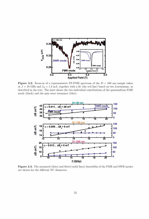
Figure 3.2: Zoom-in of a representative ST-FMR spectrum of the D = 160 nm sample takenat f = 18 GHz and Irf = 1.3 mA, together with a fit (the red line) based on two Lorentzians, asdescribed in the text. The inset shows the two individual contributions of the quasiuniform FMRmode (black) and the spin wave resonance (blue).
Figure 3.3: The measured (dots) and fitted (solid lines) linewidths of the FMR and SWR modesare shown for the different NC diameters.
31

Figure 3.4: Measured (dots) and calculated (solid lines) resonance fields of the FMR and SWRmodes for the different NC diameters. The black solid line is a fit to an average of the FMR modefor all three devices. Inset: A plot of the fitted NC diameter (D′) vs. the nominal diameter (D),together with a line indicating D′ = D.
3.1.4 Fit frequency-field dependency of satellite peak with disper-sion relation
The frequency versus field dependence of the measured FMR and SWR modes is summa-rized in Figure 3.4. The black solid line shows the average behavior of the FMR mode forall three NC diameters, essentially reproducing Figure 3.1. For a fixed frequency, we findthat the SWR mode shifts to lower fields as the NC diameter decreases. Assuming thatthe origin of the SWR mode lies in the exchange interaction, the diameter of the NC, D′,can be estimated using the dispersion relation, Equation (1.12). The room temperaturevalue of the exchange stiffness is set to A = 11 pJ/m [86]. The estimated sizes of the NCsare in reasonable agreement with the corresponding nominal values, as shown in the insetto Figure 3.4.
3.1.5 Micromagnetic simulations
Micromagnetic simulations were performed using the mumax3 solver [87]. Since the actualspin-valve mesa is too large to be simulated in its entirety in a reasonable time frame,calculations are limited to a 5.120 µm × 2.560 µm × 4 nm volume with periodic boundaryconditions tailored to mimic the lateral aspect ratio of the experimental spin-valve mesa.
32

To break the symmetry of the system, which might otherwise entirely prevent any STT-related effects and nonconservative SW scattering, the applied field is assumed to point 5◦out of plane, comparable to the possible error in the experimental field alignment. As afirst step, the evolution of the ground state of the entire Co/Cu/NiFe stack is calculated,confirming that (i) the Co and NiFe layers remain virtually collinear in the given range ofthe applied magnetic fields, and (ii) there are no mutual stray fields produced between thelayers in the vicinity of the NC. Since there is a significant spin wave-dispersion mismatchbetween Co and NiFe, any resonant dynamic magnetic coupling between the layers is notexpected. Under these three considerations, the dynamics of the NiFe free layer is simulatedalone.
Figure 3.5: (a) Normalized measured mixing voltage (Vmix) and (b) normalized simulated mag-netization precession amplitude for the three NC diameters as a function of the applied in-planemagnetic field. (c) Spatial maps of magnetization precession amplitude (top row) and phase (bot-tom row) simulated for a D = 160 nm NC diameter taken at the fields corresponding to the mainpeak and its 12 and 14 heights (as shown by the corresponding black symbols in (b)). Propagatingspin waves are clearly seen for the two lowest fields.
33

In the simulations, the experimental data acquisition routine is replicated by performingthe field sweeps with a harmonic excitation of f = 18 GHz. The infinite wire approximationwas used to calculate the Oersted field produced by the NC [88, 19]. For every value of theapplied field, the system is allowed to reach the steady state, before sampling the spatialmap of the magnetization for the following 5 ns at 3.5 ps time intervals with a subsequentpointwise FFT applied and the amplitude and phase of the magnetization precession ex-tracted at the excitation frequency. Where applicable, the direction of the spin-currentpolarization was assumed to be collinear with the magnetization in the nominally fixed Colayer. The set saturation magnetization, gyromagnetic ratio, and damping constant wereestimated by fitting a Kittel equation to the experimental data. The room temperaturevalue of the exchange stiffness was set to A = 11 pJ/m [86].
3.1.6 Anisotropic nature of spin waves propagation
The simulated magnetic response shown in Figure 3.5(b) agrees well with the experimen-tally measured data shown in Figure 3.5(a). To identify the origin of the observed peakasymmetry, the spatial profiles of the magnetization precession amplitude in the vicinityof the resonance is investigated(see Figure 3.5(c)). The snapshots clearly show that SWspropagate on the low-field side of the main peak, while no SWs are resolved on the high-fieldside. Looking closer at the phase profiles of the corresponding modes, which essentiallydepict the wavelength of the excited magnons, the following conclusions can be made: (a)the propagation of SWs perpendicular to the saturation direction is suppressed and (b)the lowest excited mode is not uniform, but rather antisymmetric with respect to the NCcenter.
3.1.7 Dependence of coexistence band of magnetostatic and exchange-dominated SWs on the thickness of FM layer
If the free layer is magnetized in-plane, then both backward volume magnetostatic SWs(BVMSSW) and surface magnetostatic-exchange SWs (SMSSW) can be excited: see Equa-tions (1.9) and (1.10), which are calculated for propagation along and perpendicular to thesaturation direction, respectively. The exchange contribution is included by substitutingB → B + µ0Ms (λexk)
2.The corresponding dispersion relations are shown in Figure 3.6 for a Py thicknesses, d,
of 100 nm (green lines) and 4.5 nm (red lines). There is always a region of resonance fieldswhere magnetostatic and exchange-dominated SWs coexist, as highlighted by the shadedarea in Figure 3.6 for the Py thickness of 100 nm. Although the band is broad for relativelythick layers, it only amounts to 1.16 mT for the 4.5 nm Py—i.e., an order of magnitudesmaller than the intrinsic broadening of the FMR peak. We therefore conclude that theSWs contributing to the low-field tail of the FMR peak are exchange-dominated. Notethat the calculated dispersion relations differ from what is found using Equation (1.12)(the thick solid line in Figure 3.6). This difference arises as the dispersion relations also
34

Figure 3.6: Dispersion relations for SWs propagating parallel and perpendicular to the saturationdirection for the different thicknesses of the NiFe layer. The points correspond to the minimumof the SW group velocity.
strongly depend on the exact boundary conditions at the free layer surfaces. For instance,if the NiFe film is pinned on both surfaces—that is, if it is placed between sufficiently thickmetallic layers—the dispersion of the exchange-dominated backward volume SWs is givenby the following equation (shown by the dotted line in Figure 3.6) [89]:
fBVMSSW-pinned =
[ (fB + fM (λexk)
2)× (fB + fM (λexk)
2 +fM
1 + (kd/π)2
)]1/2(3.1)
Note that, in this case, the spectrum of the exchange-dominated surface SWs will bedispersionless and experimentally inaccessible.
Since Equation (1.12) fits the NC diameter reasonably well, we conclude that (a) thedetected mixing voltage is generated by the exchange-dominated backward volume SWsand (b) there is undoubtedly some surface pinning of the NiFe layer. Determining theexact origin of the pinning and its strength are beyond the scope of the present study.
3.1.8 Oersted field: the main origin of magnetodynamics
Due to the collinear free and fixed layers, we do not expect any significant contributionfrom the ST to the observed magnetization dynamics; this is confirmed by comparingmicromagnetic simulations including and excluding ST. Correspondingly, for the in-planeapplied magnetic fields in the NC geometry with no dc bias currents applied, the rf Oerstedfield is the primary excitation mechanism responsible for the observed dynamics.
35

Figure 3.7: (a) The spatial distribution and (b) the corresponding 2D FFT of the out-of-planecomponent of the Oersted field by the D = 160 nm diameter NC. (c) The Oersted field as afunction of the wavevector component along the saturation direction is shown for the D = 160nm diameter NC. The inset shows a zoom-in of the small wavevector part of the spectrum. (d)Dispersion relation of the exchange-dominated SWs. (e) Experimentally acquired magnetizationdynamics spectrum using a nanocontact of D = 160 nm diameter.
In a linear approximation, the response of the system is essentially determined by thespectrum of the excitation, which in our case is provided by the rf Oersted field. If theexcitation has a finite amplitude at some point of the reciprocal space (i.e., at the givenfrequency and wavevector) then the corresponding magnon will be excited, if allowed. Thespatial profile of the Oersted field and its spectrum for the D = 160 nm NC are shown inFigure 3.7(a) and (b), respectively. We can identify both local and global antisymmetrieswith respect to the NC center with corresponding periods determined by twice the NCdiameter and mesa width, L, respectively. Since both spatial components are naturallyconfined to their unit periods, the linewidth of the corresponding excitation peak is finite.The Oersted field thus couples most efficiently to the SW bands with widths of 2π/L and
36

π/D corresponding to the wavevectors of 2π/L and nπ/D, respectively, where n = 1, 3, ...(see Figure 3.7(c) and its inset). As the NC diameter decreases, the position and widthof the former band stay constant, while the latter band shifts towards lower resonancefields and increases its width, leading to the observed extension of the tail in the excitationspectrum.
It is important to mention that the circular NC cannot effectively couple to the uniformFMR. Instead, the main peak observed in the experiments and simulations correspondsto the antisymmetric mode with k = 2π/L. However, due to the vanishing magnetostaticdispersion, its resonant field is virtually indistinguishable from the uniform k = 0 FMRmode.
3.1.9 The place of cut-off wave vector in SW bands
Considering a typical FMR experiment where the excitation frequency is fixed, according toEquation 1.12, the wave vector of the generated propagating SW is ultimately determinedby the value of the applied magnetic field. As the field is swept towards zero, past thedominant FMR resonance, the NC continuously excites propagating SWs of increasingwave vectors. Since the excitation amplitude drops rapidly for low values of the appliedfield (i.e., for short wavelength SWs), the detected magnetic signal vanishes accordingly,leading to the appearance of the low-field tail (Figure 3.7(c) and (e)).
By estimating that the extent of the tail is at one-tenth of its peak amplitude, wecan project the corresponding experimentally observed applied magnetic field to the cut-off wavevector of the excitation spectrum, as schematically demonstrated by the shadedrectangles in Figure 3.7(c), (d), and (e). This gives us the cut-off wavevectors (in unitsof π/D′) of 1.93, 1.95, and 2.34 for the NCs of 90, 160, and 240 nm nominal diameters,respectively. Since these values fall roughly inside the first two fundamental SW bandsattributed to k = 2π/L and k = π/D, the two-peak scheme used to fit the experimentaldata is fully justified.
3.1.10 NC diameter dependence of the FMR and SWR inhomo-geneous broadenings
Finally, the NC size dependence of the FMR and SWR inhomogeneous broadenings shownin Figure 3.3 can be well understood by assuming that they are inherited from the linewidthof the corresponding excitation peaks. For the SWR mode, the expected extrinsic contribu-tion to the magnonic linewidth is 96 mT, 43 mT, and 15 mT, respectively, for NC diametersof 82 nm, 122 nm, and 205 nm; this is in excellent agreement with the fitted values. Incontrast, for the FMR, the contribution is vanishing and should be virtually independent ofthe NC size. However, if the NC had shape imperfections, the corresponding irregularitiesin the Oersted field profile should broaden the excitation peaks and, eventually, the FMRand SWR. As we typically observe a less perfect NC for smaller diameters, the inhomo-geneous broadening of FMR should increase accordingly, consistent with the experimentaldata.
37

3.1.11 Conclusions
In conclusion, using ST-FMR techniques, an in-depth study of the magnetodynamics isprovided in a quasiconfined system—namely, an NC patterned on an extended pseudo-spin-valve film stack. The observed spectra are highly asymmetric and cannot be explainedby a single resonance mode, as has been done in the past [78, 75]. Instead, each spectrumis fit by a combination of two Lorentzians, from which the FMR mode resonance fieldand linewidth can be extracted. The secondary mode corresponds to the generation ofexchange-dominated spin waves with a wavevector inversely proportional to the NC di-ameter. The results are reproduced by micromagnetic simulations that show that the rfOersted field generated by the injected rf current is the dominant excitation mechanismof the observed magnetization dynamics. In this way, we experimentally demonstrate ahighly tunable point source of the propagating SW with the wavevectors limited only bythe resolution of the fabrication process used. This is of paramount importance for theapplications of sub-THz and THz magnonics and spintronics.
38

3.2 Tuning exchange-dominated spin-waves using lat-eral current spread in NC-STO
3.2.1 Another method for changing the distribution of Oerstedfield
In previous work, the Applied Spintronics group investigated how the current distributiondepends on the copper thickness of the bottom electrode (tCu) in NC-STNOs based onCo/Cu/NiFe stacks [90]. It is found that increasing tCu from 10 to 70 nm results in a 40%reduction in the threshold current, an order of magnitude higher microwave output power,and close to two orders of magnitude better power conversion efficiency.
In this study, we apply the theory from the previous section in order to tune the spin-wave resonance mode by changing the current distribution and, as a result, the distributionof Oersted field (HOe). We do this by varying the thickness of the bottom electrode. Weuse the same multilayer stack configuration as before, except that we change the thicknessof the bottom Cu layer. We measure the rectified spectra in an in-plane magnetic field andcompare the results with simulations.
3.2.2 Study of spin wave spectra of Py with different thicknessesof bottom electrode
The structure of pSV is the same as previously, except for the thickness of bottom electrode:substrate / Pd (8 nm) / Cu (tCu) / Co (8 nm) / Cu (8 nm) / Ni80Fe20 (4.5 nm) / Cu (3 nm)/ Pd (3 nm) with tCu = 10, 30, and 70 nm. The nanocontact size is chosen D =250 nm. TheST-FMR measurement configuration is the same as before; the rf power was maintainedat a constant low value of −10dBm to ensure that the excited magnetodynamics wasin the linear regime. The measurements were performed at a fixed excitation frequency,f = 18 GHz, while the in-plane applied field was swept from 0 to 0.5 T. Five nominallysimilar devices were measured and the spectra presented in Figure 3.8 is the normalizedmean value of those five spectra per sample.
3.2.3 Experimental results
Figure 3.8 shows the normalized mean value of ST-FMR spectra measured at a fixedfrequency of 18 GHz for five devices on each of three samples with tCu = 10, 30, and 70nm. The solid lines are fits of two symmetric Lorentzian to the NiFe peak (peak at higherfields). Based on the previous section, the effective diameter (D′) can be estimated usingthe dispersion relation, Equation (1.12).
Focusing on the free layer (NiFe) mode, the extracted effective diameter from the fitis presented in Figure 3.9. It can be seen that, by increasing tCu, the mean effectivediameter decreases monotonically and is inversely proportional to the mean linewidth,
39

Figure 3.8: (a) Normalized mean ST-FMR spectrum of the D = 250 nm device taken at f =18 GHz and P = −10 dBm for three different thicknesses of Cu bottom layer, together with a fit(black line line) based on two Lorentzians, as described in Ref.
(inset to Figure 3.9). In the previous section [91], we showed that the bandwidth of theSW package is proportional to the effective diameter.
3.2.4 COMSOL simulation
The theory extracted in the previous section predicts that the effective diameter is de-fined by the Oersted field. To test this hypothesis, we investigated how the current redis-tributes and induces HOe. To calculate the current flow and HOe in each layer of the de-vice, COMSOL Multiphysics simulation software is used with a detailed three-dimensionalfinite-element model of the NC-STNOs. The input values of the nanocontact size and Cuthickness were D = 250 nm and tCu = 10, 30, and 70 nm, respectively.
[90] show that the current from the top contact first crowds along the perimeter ofthe NC, and then spreads out laterally; by increasing tCu, the lateral current spread canbe strongly reduced. Figure 3.10 (a) and (b) show that the Oersted field increases forthicker tCu—i.e., when the current spread is reduced. In Figure 3.10(c), this amplification ishighlighted in the ferromagnetic layers by plotting the average strength of HOe in the middleof the NiFe (HNiFe
Oe ) and Co (HCoOe ) layers under the NC, normalized by HNiFe
Oe,(tCu=70 nm).
40

Figure 3.9: Mean value of effective diameter (D′) vs. thickness of Cu bottom layer. Inset:Plot of mean values of effective diameter (D′) vs. mean linewidth of SWR mode extracted frommeasurement of five devices.
Figure 3.10: (a) Detailed x component of HOe induced by perpendicular current in all layers fortCu = 10 nm. (b) The same for tCu = 70 nm. (c) Calculated average strength of HOe inducedby perpendicular current under the NC in the middle of NiFe and Co layers, normalized byHNiFe
Oe,(tCu=70 nm). Inset shows the top view of the middle of the NiFe layer, of which the coloredmap indicates the x component of HOe for tCu = 70 nm. All results are for D = 250 nm.
The results show that by increasing tCu from 10 to 70 nm, the strength of the HNiFeOe
and HCoOe undergo remarkable increases of ∼30% and ∼60%, respectively, under the NC
geometry. This large increase is caused by the more uniform distribution of the Oerstedfield in the devices with thicker tCu. The Oersted field plays a key role in exciting the
41

dynamics, and the decrease in the effective diameter with increasing Cu thickness (Fig.3.10(b) must accordingly be a result of a more uniform Oersted field distribution. We cantherefore conclude that it is possible to tune the SWR by tailoring the lateral current.
3.2.5 Conclusions
In conclusion, I have studied the tuning of spin-wave resonance excitation in nanocontactspin-torque oscillators. Our findings show that by changing the spread of the lateral cur-rent, the spatial characteristics of the resulting spin-wave beams can be controllably tuned.The effective diameter (which is inversely proportional to the mean of the wavevector) de-creases with increasing Cu bottom layer thickness. It can be concluded that the spreadof current must be greater for the lower thickness of the Cu underlayer at the NiFe site,which our simulation results also confirm. The spin-wave resonance linewidth increaseswith the increasing thickness of Cu bottom layer. This is connected to the first conclusionand confirms the theory presented in Section 3.1.
42

Chapter 4
Exchange coupling between two FMlayers
The systematic variation of the strength and oscillation period of indirect magnetic ex-change coupling (IEC) between adjacent ferromagnetic layers in a multilayer structurehas been studied for a decade [92, 23, 93, 28, 94, 32], due to its potential application ingiant magnetoresistance (GMR) based read heads and magnetic random access memory(MRAM). In FM/NM/FM trilayer structures, the material and thickness of the interlayerplay the key role in the type of interlayer coupling, which may be either ferromagnetic(FM) or antiferromagnetic (AFM).
In exchange-coupled samples, the optical mode is normally only observable when thecoupled layers have different resonance frequencies (fFMR)—e.g., as a result of having dif-ferent saturation magnetizations or anisotropies—although it is also possible to detect thismode for identical layers using so-called longitudinal FMR[94].
Spin pumping in coupled layers has been extensively studied [95, 96, 97, 98], but the ma-jority of those investigation have focused on the regime where the static coupling betweenthe layers is very weak or on one or a limited number of frequencies.
In this chapter, based on Co/Cu(t)/Py trilayers with tCu in the range from 0 to 40 Åandwith help of broadband conventional FMR measurement, I first study the interplay betweenthe static and dynamic interlayer exchange within the in-plane applied field. In this case,field–frequency dependency of the modes do not coincide with each other, except at zerofield-frequency. I focus on the variation of spin pumping and IEC with the thickness ofinterlayer and also with the range of applied field. Based on exchange coupling values ex-tracted from the analysis, samples are categorized into four regimes: strong, intermediate,weak, and zero coupling.
Second, based on the same set of samples and with the help of broadband conventionalFMR measurement, I am focused on the collective dynamics of the trilayer when the FMRfrequencies of the separate layers form a cross-point (CP) at a particular value and angleof the applied magnetic field, while being substantially different otherwise. To achieve thisgoal, the field is applied with the angle θ = 82◦ , where CP takes place at µ0H = 1.15T ,f = 13GHz.
43

Finally, in last section, I study the magnetodynamics in a nanocontact (NC) on Co/Cu(t)/PypSV for tCu= 20 Åby taking tCu= 80 Åas a reference sample in the same configuration ofapplied field in second section—i.e. with θ = 82◦. I excite the Co/Cu/Py NC-STO systemwith rf current using the ST-FMR measurement technique and characterize the observedfeatures.
44

4.1 Tunable spin pumping in exchange-coupled mag-netic trilayers
4.1.1 Fit of individual layers with Kittel equation
The FMR measurements were performed by sweeping the external in-plane field at fixedfrequencies, varied step-wise from 3 to 37 GHz. A fit of the derivative of an asymmetricLorentzian, Equation (2.6), to the signal provides the resonance field (µ0Hr), the full-width half-maximum (∆H), and the amplitude (A) of the absorption peak. The Kittelequation [99], Equation (2.3), was subsequently fit to the resonance frequencies of the singlelayer samples:
The results of the fits gave the following magnetic properties of Py: γ/2π=29.0 GHz/Tand µ0Meff=0.89 T and of Co: γ/2π=30.8 GHz/T and µ0Meff=1.56 T. The additionalfields are on the order of 2 mT for both samples.
Figure 4.1: FMR frequency as a function of field for the Cu-7.5 Åsample. The data (filledsymbols) is compared to three different models. The behavior at all field values is well describedby a fit of Eq. 1.18 to the data, using J ′ = 0.4 mJ/m2. The transition from collective to single-layer-like precession is illustrated by two fits using the Kittel equation, where the magnetizationand gyromagnetic ratio are fixed either to the values of single Py and Co, or to the volume meanof these layers. The effective field was used as a free parameter.
4.1.2 Fit of multilayers with free energy numerical model
For multilayers, we used a numerical model (1.18) to fit the data. We have followed theequations presented in Ref. [30] and [31], and the results show a clear correspondence
45

with the data (see Fig. 4.1). Nevertheless, the Kittel equation still sheds some light onthe nature of the oscillations. At high fields, the frequency follows the predictions usingthe magnetization and gyromagnetic ratio of the single films, while the trend of the lowfr matches the behavior of an effective medium with an Meff and γ given by the volumeaverage of the two materials. This implies a transition from a region (low fr) governed bycollective motion to one where the inherent properties of each layer dominates.
Figure 4.2: The interlayer exchange coupling (J ′) as a function of spacer layer thickness. J ′ wasdetermined by fits of Eq. 1.18 to the field dependence of the FMR frequency. Inset: FMR spectraof Cu-7.5 Å(thick black lines) together with fits of two asymmetric Lorentzians (cyan lines), andthe spectra of the single layer Co (dashed lines) and Py (dotted lines). The left and right plotsshow the absorption at 20 and 35 GHz, respectively.
4.1.3 The positive oscillatory behaviour of interlayer coupling
The derived values of the interlayer coupling are presented in Figure 4.2. The layer thick-nesses and magnetizations were fixed during the fits to Eq. 1.18, while we let J ′, γPy,and γCo vary. The resulting values of the IEC were essentially unchanged if the gyromag-netic ratios were treated as constants, but the goodness-of-fit was worse. The couplingis ferromagnetic for all tCu, in contrast to the familiar behavior where J ′ is expected tooscillate between positive and negative values. We can therefore conclude that the in-teractions between the layers are not only given by RKKY interactions, but also includeNéel (orange peel) coupling [100]. This interpretation is strengthened by the fact that weobserve a minimum at the thickness (1 nm) where a negative maximum would otherwisebe expected [101, 102].
46

Figure 4.3: Linewidth vs FMR frequency for the a) Py and b) Co resonances. The verticallines in both a) and b) mark the inflection point of the Co linewidth, which is a measure of thetransition from collective to single-layer-like behavior. The arrows show the Co-frequency at zeroapplied field. Below this frequency, there is only one resonance in the system.
4.1.4 The effect of IEC on linewidth of low frequency resonancemodes
The linewidth of the Py and Co resonances are shown in Figure 4.3a and b, respectively.For samples in the intermediate or weak coupling regime, both datasets have a distinctconcave shape, which is more pronounced for Co. The linewidth of Co not only flattens out,but also increases at low frequencies. The optical mode is expected to have a much largerlinewidth than the acoustical mode, due to spin pumping [103]. However, the linewidthof the single layer Co is not Gilbert-like, but rather saturates at a constant value. Thisbehavior is inherited in the bilayer samples. The damping of the Co mode also fluctuatessignificantly with Cu thickness, probably due to strain-induced effects beyond our control.We have consequently chosen not to dwell on the behavior of the linewidth associatedwith this material, but we do note that the increase in ∆H is consistent with an opticalcharacter of the mode.
If we follow ∆HPy (J ′ > 0) from high to low frequencies, we see that the initial con-stant slope is reduced at a certain frequency marked by a vertical line in the figure. Itis noteworthy that this frequency (finfl) also corresponds to the inflection point of the Colinewidth (Fig. 4.3b). The relative resonance intensities (see Fig. 4.4) also change drasti-cally around finfl. Both these effects are clear signs of a transition from a high-frequencyregion where the acoustic and optical modes are mostly associated with the Py and Colayers, respectively, to a low-frequency region where the precession is truly collective. Thelinewidth of the acoustic mode decreases, since it represents in-phase oscillations and thespin currents cancel, while they add up in the optical out-of-phase mode. The Co linewidthincreases accordingly. When the Co (optical) mode disappears, marked by arrows in thefigure, the slope again become constant and follows the single film behavior. The absence
47

of nonlocal damping implies that both layers precess in phase and that the sum of the spincurrents is virtually zero [26].
The Cu-40 Årepresents the samples without interlayer coupling; in such systems, thelinewidth is linear in f , as expected for a pure spin-pumping effect. The inset in Figure 4.3ashows the damping parameter of Py extracted from the linear region at high frequencies.The damping shows a weak dependence on J ′ above the spin relaxation coherence length(≈ 1 nm). Nonetheless, since α is constant for samples with no coupling, it is obvious thatthe main source of the increased damping is spin pumping.
Figure 4.4: Color map of the FMR for a) a sample with weak and b) zero interlayer coupling.The Py amplitude is lower than that of Co for all frequencies when the layers are decoupled(b). However, in the presence of IEC, the relative intensities change below 15 GHz (a). Themodification of the intensities mirrors the transition from single-layer-like behavior at high fre-quencies/fields, to a region where the precession is truly collective with acoustic (high amplitude)and optical (low amplitude) modes.
4.1.5 Study amplitude of the modes - transition to collectiveregime
The measured spectra (3–37GHz) of the Cu-8.8 Åand Cu-40 Åsamples are presented inFigure 4.4a and 4.4b, respectively. The intensity of the signal is dependent on both theprobed magnetic moment and the frequency. We have therefore normalized the amplitudeat each frequency. The Co mode of the Cu-40 Åsample is stronger than the Py modeat all frequencies, as expected considering the smaller magnetization and thickness of thePy layer. The presence of interlayer coupling gives a different picture. For Cu-8.8 Å, theamplitude of the Co mode quickly decreases below ≈ 15 GHz. This reveals the transitionto a region where the Py and Co show distinct acoustic and optical mode characteristics,in accordance with the interpretation of the frequency dependence of the damping.
48

4.1.6 Conclusion
In this study, I investigated the interplay between IEC and spin pumping, using Co/Cu/Pypseudospin values. I showed that the hybridization between the layers, leading to acousticaland optical modes, is not only dependent on the IEC, but also on the field and frequency.The collective nature of the precessions is clear at low fields, as reflected by the relativeamplitudes and the field dependence of the resonance frequencies. At higher applied fields,the layers behave as single films subject to an effective field proportional to the interlayercoupling. This transition, from collective to single layer precession, is accompanied bychanges in the slope of ∆H vs. f , (i.e., the damping), and I attribute those changes to thespin pumping between the layers. The results demonstrate that it is possible to engineera cut-off frequency, below which the spin pumping is effectively turned off.
49

4.2 From individual to collective behavior in multilay-ered magnetic structures in the vicinity of the reso-nance coincidence point
This section is organized as follows: First, I describe our experiment and model details,then I show the colormap plot of the field-frequency dependency of three samples (eachrepresentative of one regime), and finally I study the linewidth and amplitude behaviorof the modes in each regime in comparison with individual layers and fit with the Francomodel (see Section 1.2.4).
4.2.1 Experiment and numerical model of Kittel equation for fitin an oblique field
The FMR measurements were carried out in the range of f = 2–20 GHz. I fixed thenominal angle between the field and the sample plane to 82◦. This angle was chosen toobtain a coincidence point of the Co and NiFe resonances in a frequency and field rangewell within the limits of the setup. The sample structure and measurement configurationis illustrated in Figure 4.5.
Figure 4.5: a) Schematics of the sample structure and b) the FMR setup configuration. c)Calculated angles of the magnetization in single Co (red solid line) and NiFe (black dashed line)layers using Eq. 2.4. The blue dotted line shows the difference between the two angles; the verticaldashed lines marks the field of the linewidth maxima.
The FMR signal was fit using equation (2.6). The FMR frequency of a thin magneticfilm can be described by equations (2.4) and (2.5). The result of fit to the single layersare: µ0MCo = 1.68 T, γCo/2π = 29.2 GHz, and µ0MNiFe = 0.81 T, γNiFe/2π = 28.3 GHz.The actual field angle was treated as a free parameter and the best fits were obtained forθH = 83.5◦—i.e., very close to the nominal value (Fig. 4.5(c)). The anisotropy was assumedto be zero. The extracted parameters were subsequently used to calculate the internaltilting angles of the magnetizations in uncoupled layers (Fig. 4.5). The maximum relative
50

angle θNiFe − θCo = 33◦ occurs at a field (µ0Hext = 1.05 T), close to the experimentallydetermined CP at µ0HCP = 1.15 T.
4.2.2 Numerical model for exchange coupled multilayers
The strength of the IEC is determined in the present samples in Section 4.1 using in-planemeasurements; the samples were divided into four groups of different coupling strength:strong, intermediate, weak, and zero coupling. Although the strong and intermediateregimes display very similar behavior in this study, I have chosen to keep the same nota-tion for consistency, the only exception being that I call the last category “very weak” tohighlight that the samples may have a tiny residual coupling. The model employed to fitthe value of J ′ in this study is one recently developed by Franco and Landeros [32], butthe results are similar to those from the previous section. The parameters extracted fromthe fits of the Kittel equation (2.4) to the data of the single layers were used as fixed inputparameters and J ′ is the only free variable in the subsequent fits utilizing the model inRef. [32].
Figure 4.6: Color maps of the FMR spectra of samples with spacer layer thickness (a) tCu = 10 Å,(b) tCu = 8.8 Å, (c) tCu = 8.1 Å. Signal strength is normalized to -1 at each frequency to highlightthe relative intensity of the modes. Note: the weak feature in Cu-8.1 Å, which appears above13 GHz, is not the optical mode, but an unidentified mode.
4.2.3 Three distinctly different regimes
The raw FMR data of selected samples, representing three regimes of coupling strength,is presented as colormaps in Figure 4.6. The different sample categories demonstratedistinctly different behaviors: the Cu-10 Åsample has two modes, which keep their re-spective character after the CP; the acoustical and optical nature of the modes in theCu-8.8 Åsample is indisputable; the Cu-8.1 Åsample has only one mode in the measured
51

Figure 4.7: Resonance field (µ0Hr) as a function of frequency (f). The open symbols denoteCo/optical modes, while the closed symbols show the NiFe/acoustical modes. The inset in (b)shows ∆f = fop − fac versus field. The Cu-8.1 Åmode indicated by the blue triangles is neitheran acoustical nor an optical mode, but an unidentified mode.
field and frequency range. This sample also displays a weak feature above the CP. We havenot been able to identify this mode, but include it in the following figures for completeness.
4.2.4 Field-frequency dependency characteristics of each regime
The different behavior in the three regimes is further emphasized in Figure 4.7, where theresonance fields are presented. It is indeed possible to roughly estimate the strength of theIEC merely by inspecting the data. The stronger the coupling, the larger the shifts to lowerresonance fields compared to the single layers. It is, however, not easy to distinguish whichof the two samples in the weak coupling regime has the highest IEC. The acoustical modesfollow each other closely, while the shift in the optical mode is higher for Cu-8.8 Åbeforethe CP and smaller above. Trilayers with a notable IEC exhibit a frequency gap, whichincreases with increasing J ′. The inset in Figure 4.7(b) shows the frequency differencebetween the optical and acoustical modes (∆f = fop − fac) as a function of applied field(i.e., the resonance field). The larger frequency gap of Cu-16.2 Åshows that the IEC isstronger in this sample than in Cu-8.8 Å.
The observed frequency shift of both modes is always higher before the CP than after.We calculated the frequency shift to elucidate this point. The results are found in Figure 4.8and show that the optic mode continuously shifts to higher frequencies as J ′ increases.The acoustic mode, on the other hand, is limited by a maximum frequency before thecoincidence point and only exhibits tiny shifts after the CP. The calculations do not explainthe inconsistent shifts mentioned in the paragraph above, and this might imply that theCo layers in the two samples are not completely identical.
The IEC strength of the samples was determined by fits using the model presented inRef. [32] (see Fig. 4.9). The model captures the experimental results well when J ′ is small,but deviates more as the coupling increases. Nonetheless, the estimated values allow us to
52

Figure 4.8: Calculated frequency shift due to interlayer exchange coupling (J ′) for the acoustical(solid lines) and optical (dashed lines) modes. Two different fields are compared, µ0H = 0.7 T(black lines) and µ0H = 1.3 T (red lines), representing resonances that occur before and after thecoincidence point (CP).
Figure 4.9: Fits of the model given in Ref. Franco2016 (lines) to the data (symbols). TheNiFe/acoustical resonance fields are presented by solid symbols, while the Co/optical modes aredenoted by open symbols. The data for Cu-8.8 Åand Cu-8.1 Åare offset by 0.7 and 1.4 T,respectively. The fitted values of J ′ are 0.016, 0.07, and 0.87 mJ/m2 for the Cu-10Å, Cu-8.8Å,and Cu-8.1 Åsamples, respectively.
quantify the coupling strength in the different regimes: crossing of the modes occurs forJ ′ < 0.02 mJ/m2 (very weak IEC), clean optical modes are observed when J ′ ≈ 0.1 mJ/m2
(weak IEC), and they are pushed far away from the Co resonance for coupling strengthshigher than J ′ ≈ 0.8 mJ/m2.
53

Figure 4.10: The frequency dependence of the linewidth (∆H) for samples in different regimes.The inset in (a)left shows ∆H in the frequency range 8–22 GHz, together with a linear fit. Theinset in (b)left shows ∆H as a function of field. The linewidth of the unidentified mode inCu-8.1 Åis shown by blue triangles in (c).
54

4.2.5 Linewidth-frequency dependency characteristics of each regime
The linewidth of the single films is shown in Figure 4.10. Both NiFe and Co display largepeaks in ∆H, but at different frequencies. The maximum in ∆HCo coincides with the CPfrequency by chance; the two are not directly related. The peak maxima of NiFe and Cooccur at µ0H ≈ 0.6 and 1.2 T, which correspond to the magnetization angles θint = 42◦ and37◦, respectively (see Fig. 4.5(c)). The calculated values correspond well with the expectedθint = 45◦, despite the simplicity of the model.
The overall shape of the ∆H(f) curves is preserved in the very weak coupling regime(Fig. 4.10(a)), and each mode closely follows the behavior of the respective single film. Theinset in Figure 4.10(a) shows the linewidth of NiFe and Cu-40Å, together with a linear fit.The damping constant of both samples is similar, which implies that spin pumping effectsare either ineffective in this frequency/field range or that the spin-sink efficiency of theCo and the cap layers is equal. The latter requires that the thickness of the top Cu layeris smaller than the spin diffusion length (λsd). However, λsd of the sputtered Cu films issmall and the spin-pumping contribution to α decreases rapidly for tCu > 10 Å[95]. Thisis confirmed by the in-plane measurements, since the damping constants are higher for thetrilayers than for the single NiFe (Section 4.1). Furthermore, the frequency dependenceof the in-plane linewidth clearly shows that the linewidth broadening is dominated byspin pumping effects, not two-magnon scattering. We must therefore conclude that spinpumping is suppressed above µ0H > 1.3 T.
The evolution of ∆H(f) in the weak coupling regime reflects the transition from NiFe(Co) to Co (NiFe) dominated acoustic (optical) modes (Fig. 4.10(b)). The linewidths ofthe acoustic modes peak at the same field as for NiFe (see inset to Fig. 4.10(b)), implyingthat the coupling to the Co layer is too weak to change the field dependence of θNiFe
int .The onset of the second peak corresponds to the minima in ∆f—i.e., the position of thefrequency gap. The linewidth increases rapidly above this point and decreases again whenthe transition is complete. The optical mode displays a sharp drop in the same frequencyrange. Before the CP, the linewidth of this mode is much larger than ∆HCo—a clearsign of out-of-phase precession combined with spin pumping [100, 104, 97]. Likewise, thelinewidth is enhanced compared to ∆HNiFe after the CP.
The linewidth is the only parameter differentiating the samples with strong and in-termediate coupling in this study. The strongly coupled layers display a single peak in∆H (Fig. 4.10(c)), signifying a coherent rotation of the magnetization in both layers. Thelinewidth approaches the NiFe values at high frequencies. Unfortunately, it is not possibleto determine whether the damping is lower or higher than in the single NiFe film, due tothe limited field range. For intermediate coupling, the bimodal shape of ∆H shows thatthe magnetization rotation is neither coherent nor governed by the single layers. The mag-netization direction must instead vary continuously throughout the layers, as in exchangesprings [105].
55

Figure 4.11: The amplitude of the absorption signal for samples belonging to different regimes.The linewidth of the unidentified mode in Cu-8.1 Åis presented by blue squares on a green line.
4.2.6 Amplitude-frequency dependency characteristics of each regime
The amplitude of an FMR signal and its frequency have a complex dependence on theproperties of the measurement setup and the sample details. Nevertheless, if the data is
56

collected using the same setup, settings, and samples, the main contributions to a highamplitude are: a short distance to the source of the excitation field, a large total magneticmoment and (for multilayers) a large coupling strength [100]. The latter only holds forthe acoustic mode; the optical mode shows an opposite trend and its intensity weakens.Figure 4.11 shows the amplitude as function of frequency, and the samples in each categoryagain show similar behavior.
In the very weak coupling regime, a striking feature is observed as f → 0: the intensityof the NiFe mode increases rapidly, while the Co mode declines, as shown in Figure 4.11(a).This hints of increased coupling between the layers. Moreover, the linewidth of the Co modeincreases simultaneously and ∆H of the NiFe mode decreases faster than for the single film(Fig. 4.10(a)). Taken together with the in-plane data in Section 4.1, this can only be a signof a transition to a collective precession. The origin of the emergence of collective modesis the so-called dynamic exchange coupling (DEC), which is generated by spin pumpingand appears close to resonance coincidence points[106, 104, 97]. We use the notation CPto describe the resonance crossing at f ≈ 13 GHz, but fNiFe and fCo also approach eachother at low fields, allowing for the onset of dynamic exchange. The intensity of the NiFemode increases slightly when the frequency comes close to the CP from below, while bothmodes closely follow the amplitude of the individual layers above the CP. This is consistentwith the suppression of spin pumping at high frequencies and fields, as discussed above.
An evolution of the collective/individual nature of the modes can also be seen for theweak regime. The amplitude of the acoustic mode in the samples with weak IEC is high atlow frequencies, while the optical mode is absent (f op(H = 0) ≈ 6 GHz). The presence ofdynamic exchange will thus not alter the nature of the precession, and it is not possible todetect the existence of DEC for f → 0. However, the decline in this coupling with increasingfrequency is clearly visible in Figure 4.11(b). The amplitude of the acoustic mode decreasesabove f = 7 GHz while the optical mode increases, in accordance with a lower effectivecoupling and a less collective behavior. At higher frequencies, the amplitude of bothmodes increases. This marks the onset of the transition between governing layers. Thelarger magnetic moment of the Co layer leads to a higher A compared to NiFe. Hence, thetransition from NiFe-dominated to Co-dominated, as well as the more individual characterof the optical/Co mode, will lead to an increase in A, as long as the optical mode is stillmostly associated with the Co layer. There is no spin pumping above the CP and theacoustic mode has a high amplitude, whereas the A of the optical mode is smaller thanfor the single NiFe layer, as expected. The amplitude of the acoustic mode in samplesbelonging to the strong/intermediate regime is close to ACo for the whole frequency range,as shown in Figure 4.11(c). It is therefore impossible to draw any firm conclusions aboutthe DEC and the plausible mode transition. The acoustic nature of the mode is, however,evident.
4.2.7 Conclusion
In this study, the magnetic field was applied at an out-of-plane angle of 82◦ to facilitate acoincidence point where the resonance field and frequency of Co and NiFe are equal. I ob-
57

served three distinctly different regimes in coupling strength: very weak (J ′ < 0.02 mJ/m2),weak (J ′ ≈ 0.1 mJ/m2), and intermediate/strong (J ′ > 0.8 mJ/m2). The resonance fieldsclosely followed the single-layer behavior for samples with very weak coupling (tCu = 10-40 Å). However, both linewidth and amplitude showed deviations at low frequencies. Iattribute these changes to the dynamic exchange coupling that emerges when the FMRfrequencies of two magnetic layers, subject to mutual spin pumping, approach each other.The impact of this coupling was also clear when J ′ ≈ 0.1 mJ/m2, and I have shown that thepresence of the dynamic coupling always promotes a collective precession. Furthermore,the results imply that spin pumping is suppressed at high frequencies.
The modes in samples with weak IEC (tCu = 16.2 and 8.8 Å) had a distinct acousticand optical nature. Close to the coincidence point, the two modes experienced a frequencygap—a hallmark of static interlayer coupling. The anticrossing was accompanied by atransition of the governing layer for the modes, as unambiguously revealed by the linewidthsand amplitudes: Below the CP, NiFe dominates the acoustic mode and Co dominates theoptical mode; above the CP, the situation is reversed and Co dominates the acoustic mode,while NiFe governs the optical mode.
Only the acoustic mode was observed in samples with strong/intermediate coupling.The field dependence of the linewidth showed that the layers behave as a single film fortCu ≤ 5 Å, while the magnetization in layers separated by a thicker spacer is exchange-spring like.
58

4.3 Effect of microwave current on resonances of cou-pled Py/Cu/Co trilayers in oblique magnetic fields
In this work, we use the ST-FMR technique to study the effect of the rf current on themagnetodynamics in the vicinity of the coincidence point of the NiFe/Cu/Co multilayers.We chose spacer layers thick enough to avoid the RKKY interaction between the two FMlayers: that is, thicknesses of 2 nm and 8 nm, with the latter being a reference for theformer.
In particular, we investigate two distinct regimes: (a) decoupled, by using a sufficientlythick Cu layer of tCu = 8 nm to avoid the RKKY interaction between the two FM layersand (b) weakly coupled, for tCu = 2 nm, using the former as reference to study the latter.
Figure 4.12: (a) Layout of the NC-STO and the spin torque FMR (ST-FMR) measurementsetup. (b) Frequency vs. in-plane field dependence of the Co and Py FMR peaks for the sampleswith Cu spacer layer thickness of 8 nm and 2nm. (c) Simulated Co and Py FMR frequenciesversus strength of the magnetic field at θ = 80◦ out-of-plane.
4.3.1 Sample layout and experimental setup
The layout of the NC-STO is demonstrated in Figure 4.12 (a); NCs of nominal diameter400 nm are defined through the SiO2 insulating layer using e-beam lithography at thecenter of the mesa. We chose a relatively large NC to reduce the linewidth and asymmetryof the excited peaks caused by the excitation of the SWR.
All measurements were performed at room temperature in a custom-built probe stationutilizing a uniform magnetic field of up to 2 T. Our ST-FMR measurements schematic isshown in Figure 4.12 (a) and details can be found in Section 2.2.3.
4.3.2 Characterization of samples in in-plane field configuration
We first characterized our samples using in-plane applied fields. For this purpose, we chosea spacer layer thick enough to suppress any means of the coupling between the layers, toensure they behave similarly to free-running films. The FMR frequency dependencies are
59

Figure 4.13: Colormaps represent the field vs. frequency dependence of the mixing voltagemeasured for a) tCu = 8 nm and b) tCu = 2 nm for the applied field at θ = 80◦ out-of-plan. Theblack and red dashed lines show the FMR of the Py and Co layers extracted from the tCu = 8nm sample.
fitted using Equation (2.3). The results of this fit are shown in Figure 4.12b and the valuesof the extracted parameters are summarized in Table 4.1.
Thickness of spacer, nm µ0Ms, T γ, GHz / T µ0Hadd, mT
Py 8 0.746 29 0
Co 8 1.100 31 0
Py 2 0.746 29 0.032
Co 2 1.100 31 0.110
Table 4.1: Summary of magnetic parameters extracted from fitting the in-plane ST-FMR datato the Kittel model.
4.3.3 Characterization of samples in out of plane angle of the field
Using Equation (2.4) and (2.5), we then calculate how the FMR frequencies behave withthe field applied θ = 80 out-of-plane.
The results of this calculation are shown in Figure 4.12c. We observe that Co andPy FMRs curves cross at the frequency and resonance field of around f = 15 GHz andµ0H = 1.2 T, respectively. In fact, our ST-FMR measurements on the tCu = 8 nm sample(see Fig. 4.13a) are in good agreement with the theoretical estimate.
60

Figure 4.14: ST-FMR spectra of the samples with spacer thickness of (a) 2 nm and (b) 8 nm,acquired at a fixed rf current frequency of 18 GHz for different applied field angles. Insets showfitted amplitude of the observed resonances.
Figure 4.15: ST-FMR spectra of the sample with the Cu spacer thickness of 2 nm measured soas to keep the resonance field of the sharp peak constant. This demonstrates how the resonancefield difference with the FMR mode increases with the applied field angle.
Figure 4.13a shows that there is neither anticrossing nor reduction of the linewidth of thepeaks at the coincidence point, consistent with our regular FMR measurements. This again
61

confirms virtually the decoupled dynamics of the layers and suggests a vanishing dynamicexchange coupling[107]. The observed increase of the mixing voltage at the coincidencepoint happens as the dc signals of both layers add up. It is worth noting that the Py andCo peaks have significantly different line shapes. According to Kupferschmidt et al. [108],a symmetric lineshape of the Co FMR suggests that it is detected via the spin-pumpingeffect, while the antisymmetric shape of the Py FMR highlights the dominance of the spin-diode effect. This difference suggests much stronger spin current injection from Co to Pythan the other way around.
The situation is substantially different for tCu = 2 nm. We can no longer resolve theCo FMR in the measured frequency range; instead, we observe a broad Py FMR peakaccompanied by a rather sharp mode shifted to higher frequencies (see Fig. 4.13b). Bothgo virtually in parallel with the rf frequency, suggesting that the sharp peak originatesfrom the Py layer.
The same qualitative behavior is observed for both Cu thicknesses when we fix thefrequency of the ST-FMR and instead sweep the applied field angle (see Fig. 4.14). Inthis case, however, the sharp mode only appears in the vicinity of the coincidence point,starting at roughly 75. If we now change the frequency of the microwave current, wecan observe the mode in the much broader range of applied field angles. For the sake ofcomparison, we perform our measurements in a way that the sharp mode has roughly thesame resonance field. To do this, for the given angle of the applied field of µ0H = 1.26T ,we performed a frequency sweep measurement to find the exact position of the sharp peak.We then carried out a field sweep measurement at the same frequency as the sharp peak,as shown in Figure 4.15. This plot reveals how the sharp peak appears in the vicinity ofthe Py FMR, starting from an applied field angle of roughly 60. As the angle increases to80, the linewidth of the sharp mode drops significantly to µ0∆H = 0.8 mT, and the FMRmoves away from it to higher fields. As we increase the angle further, the distance betweenthe two modes remains virtually the same (around 0.1 T), while the linewidth of the sharpmode gradually increases.
4.3.4 Discussion
To understand the nature of the sharp mode, we first note that, irrespective of the appliedfield angle and microwave frequency, this mode appears above the Py FMR mode. Aswe seen before, a weak positive coupling between the layers might transform the FMRmodes of the individual layers to the collective resonances that are shifted to the higherfrequencies (see Section 4.1). However, the splitting between the sharp and broad peaksat the coincidence point is (a) too large to be attributed to the weak RKKY interactionat tCu = 2 nm and (b) cannot be related to the dynamic exchange coupling, as it shouldremain virtually the same for tCu = 8 nm (i.e., it decays substantially only if the Cu spacerthickness is on the order of its spin diffusion length of 100 nm–1 µm[109]). Furthermore,as both modes show virtually the same frequency vs. field slope, they should belong to thesame magnetic layer (Py in this case).
In fact, the sharp mode is observed in the band of the propagating spin waves, similar
62

Figure 4.16: (a) ST-FMR spectra versus rf current power of the sample with 2 nm spacer layerand (b) the corresponding fitted resonance fields and linewidths of the sharp and FMR modes.
to the Oersted-field-driven SWR we found for the magnetic field applied in-plane. Thesubstantial difference, however, is that we found a mean linewidth for the Oersted-drivenFMR and SWRs of around 15 mT and 25 mT, respectively, for the NC diameter of 240 nmand a microwave frequency of 18 GHz. The observed sharp peak is thus much narrowerthan the typical linewidth of the linear resonances and cannot therefore be attributed tothe more coherent linear excitation of SWs, due (for example) to the larger NC diameter.So there should instead be some antidamping mechanism at play that reduces the intrinsicmagnetic losses beneath the nanocontact.
To reveal the properties of this mechanism, we measure how the response of the systemevolves with the applied current power, as shown in Figure 4.16a. Both the FMR andthe sharp mode exhibit nonlinear behavior. In particular, both types of resonance expe-rience blueshifting of their resonance frequencies, suggesting positive nonlinearity. Thisis consistent with the theoretical estimations for the similar Py film[64], as in our casePy is saturated at 80 out-of-plane, which is well above the linear magnetization angle ofθ ≈ 60 at which the nonlinearity turns from negative to positive.
While moderate changes of the FMR resonance field and substantial increase of itslinewidth might be attributed to the nonuniform Joule heating[110], this would not explainwhy the sharp mode experiences significantly larger blue-shifting and, most importantly,a dramatic reduction of its linewidth (see Fig. 4.16b). At the same time, for sufficientlylarge applied currents, the rf Oersted field might drive Py modes to the nonlinear regimewhere the so-called Suhl instabilities emerge[111]. Although this could explain the growthof the amplitude and the corresponding blueshifting of both the FMR and the sharp modes,such kind of auto-oscillations typically lead to a foldover effect[112, 113], which we do notobserve in our ST-FMR measurements. Furthermore, we expect the rf Oersted field todrive the FMR much more strongly than any SWR modes, so it should have a steeperresonance field vs. current dependence than the propagating mode. Finally, in contrast toour observations, the Oersted-field-induced effects should be virtually independent of the
63

position of the Co peak.The only possibility to explain the sharp peak thus involves spin transfer torque. In-
deed it might excite auto-oscillations even with rf currents—that is, parametrically[114].However, the microwave signal might only excite at either its half or double frequencies,i.e. 9 GHz or 36 GHz, respectively for 18 GHz pumping. The former is unlikely, as suchresonances would lie below FMR of both Py and Co for the given applied fields; the secondoption should appear at a much larger shift from the FMR than we observe experimen-tally. As with the Oersted field, we would also expect such parametric pumping to beindependent of the position of the Co peak.
At the same time, a direct spin current might provide antidamping and, in our particularcase of positive nonlinearity, lead to the nucleation of propagating spin waves, the so-calledSlonczewski mode[115]. Although this might sound counter-intuitive, since we drive oursystem with rf currents, we would like to stress again that the resonances are detectedpartially due to the spin-pumping effect—that is, a dc current that magnetization dynamicsinjects into the adjacent metallic layers. The magnitude of this effect is proportional tothe magnetization precession amplitude. In particular, we expect it to be much reducedin the Co layer for the spacer thickness of tCu = 8 nm, as most of the rf current will flowthrough Cu and the amplitude of the rf Oersted field at the Co cite will decreased.
The spin pumping from Co to Py layer should happen whenever the Co dynamics isdriven, so it should potentially drive magnetization auto-oscillations in Py even when res-onances of both magnetic layers are separated from each other. However the nature of theST-FMR measurements does not allow us to track dynamics of both layers simultaneously.So if the resonances of FMR layers are well separated, there will be no spin pumping fromthe Co layer once we tune to the Py modes and vice versa. It is thus only by bringing theresonance conditions of both layers together that we can observe the effect of antidamping.
Finally, we would like to emphasize that the observed blueshifting of the sharp modemight only occur in case of auto-oscillation. We thus conclude that spin pumping from theCo layer to the Py layer is sufficient to fully compensate magnetic losses beneath the NC.
4.3.5 Conclusion
I have observed a sharp feature at the resonance frequency of the coupled pseudo-spin-valve excited by rf current. The mode appears in the Py layer and experiences signifi-cant blueshifting of its frequency with applied current strength, consistent with positivenonlinearity of the NiFe film. Nucleation of the self-sustained propagating spin waves(Slonczewski mode) via rf-to-dc current conversion can be demonstrated. In particular,as I drive magnetization dynamics in Co and Py layers with rf current, and thus Oerstedfields, it creates a mutual DC current injection via the spin-pumping effect. This providesmutual antidamping and, for sufficiently strong rf powers, leads to the nucleation of themagnetization auto-oscillations. As the magnetization dynamics at the same frequencyare pumped and detected, the linewidth reduction and auto-oscillations might only be ob-served in the vicinity of the Py and Co resonances crossing. In this case, I detected a sharppeak with a linewidth as small as µ0∆H = 0.8 mT, and this could be reduced further with
64

higher rf current amplitudes and thinner Cu spacer layers. In fact, I observed that theauto-oscillations disappear for tCu = 8 nm, consistent with the reduction of the Oerstedfield amplitude at the Co site and suppression of the spin diode effect due to the lateralcurrent spread.
65

Chapter 5
Conclusions and future works
ConclusionsThe research presented in this thesis has centered on fundamental Spintronics researchon the pseudo-spin-valve (pSV) structure in the form of blanket film and nanocontact(NC) geometry. The main focuses were on studying the nature of the excited spin-waveresonances in in-plane magnetized NC pSVs by means of the ST-FMR technique, and thestudy of magnetodynamics in coupled pSVs in in-plane and out-of-plane applied fields bymeans of broadband conventional FMR and ST-FMR techniques. The following is a listsummarizing all the results:
Results from the study of spin waves in in-plane magnetized NC-STOs on Co/Cu/PypSVs in two sections:
1. For in-plane fields, it is the the rf Oersted field in the vicinity of the NC that playsthe dominant role in generating the observed spectra, and not the STT.
2. In addition to the FMR mode, exchange dominated spin waves are also generated.
3. The NC diameter sets the mean wavevector of the exchange dominated spin wave,in good agreement with the expected dispersion relation.
4. By changing the spread of the lateral current, the spatial characteristics of the re-sulting spin-wave beams can be controllably tuned.
5. The effective diameter (inversely proportional to the mean wavevector) decreaseswhen the Cu bottom layer thickness is increased.
Results from the study of interlayer exchange coupling between FM layers in Co/Cu(t)/PypSVs in three sections:
1. It is possible to engineer a cut-off frequency, using the strength of the IEC, belowwhich spin pumping is minimized.
66

1. By applying the magnetic field at an out-of-plane (OOP) angle, a coincidence pointwhere the resonance field and frequency of both FM layers are equal is facilitated. Dueto behaviour of governing layer around coincidence point, three distinctly differentregimes are observed in coupling strength: very weak or single layer behavior (J ′ <0.02 mJ/m2), weak or collective behavior (J ′ ≈ 0.1 mJ/m2) and intermediate/strongor alloy-like behavior (J ′ > 0.8 mJ/m2).
2. In OOP configuration, the modes in samples with weak IEC had a distinct acousticand optical nature. Close to the coincidence point, the two modes experienced afrequency gap due to a transition of the governing layer for the modes.
3. In strong/intermediate coupling regime, the field dependence of the linewidth showedthat the layers behave as a single film for tCu ≤ 5 Å, while the magnetization in layersseparated by a thicker spacer is exchange-spring like.
1. Exciting coupled NC pSVs by rf current in the OOP configuration results in a highQ=factor peak with a linewidth as small as µ0∆H = 0.8 mT in the vicinity ofresonance coincidence point.
2. The mode appears in the Py layer and experiences significant blueshifting of itsfrequency with applied rf current strength, consistent with positive nonlinearity ofthe Py film. Nucleation of the self-sustained propagating spin waves (Slonczewskimode) can be demonstrated via rf-to-dc current conversion.
3. This feature disappears for tCu = 8 nm, consistent with the reduction of the Oerstedfield amplitude at the Co site and suppression of the spin diode effect due to thelateral current spread.
Future works
ST-FMR study of frequency doubling in NCs on Heusler alloys
During my study of NCs, described in Chapter 3, I found there is a lack of fundamentalstudies of these geometries. For example, in the low-frequency field range, double frequencymode could be excited and detected easily by ST=FMR technique in NCs, and nonlinearityempowers the modes. Heusler alloys are good materials to investigate in NC geometrythrough the excitation of double frequency modes, as the effectiveness of double frequencymodes is proportional to the ellipticity of the magnetization and is most sensitive in sampleswith transverse demagnetization factors that are not equal to each other[7]. The methodcan thus serve as a good probe for studying magnetodynamics in Heusler materials.
67

FMR study of exchange coupling in FM/NM (t)/FM trilayers withdifferent NM materials in the vicinity of the coincidence point
Exchange coupling between layers and acoustic and optical modes remains a subject of ac-tive research. Clear observation of both the acoustic and optical behavior of the modes andthe tracking of the contribution of the governing layers (see Section 4.2) may lead to morecomplex studies that involve different spacer layers, such as Ru or topological insulators.This can also be further investigated through cryo-FMR at ultralow temperatures.
ST-FMR study of the sharp feature in coupled FM/NM (t)/FMtrilayers with different NM and FM materials
Observation of sharp features by means of rf current is reported here for the first time inan NC geometry on a pseudo-spin-valve structure. There is much opportunity to continuethis work experimentally by choosing different materials for the spacer layer, or even bychanging the materials of ferromagnetic layers and going deeper into the nature of themode from the theoretical point of view.
68

Bibliography
[1] F. Bloch, Zeitschrift für Physik 61, 206 (1930).
[2] G. Heller and H. A. Kramers, Proceedings Koninklijke Akademie van Wetenschappen37, 378 (1934).
[3] V. G. B. A. I. Akhiezer and S. V. Peletminskii, Science 163, 923 (1969).
[4] W. Marshall and S. W. Lovesey, Science 77, 50 (1972).
[5] D. D. Stancil, Theory of Magnetostatic Waves (Springer New York, 1993).
[6] C. Kittel, Introduction to Solid State Physics (Wiley, 1996).
[7] G. A. Gurevich, A. G. &Melkov, Magnetization Oscillation and Waves (CRC press,1996).
[8] M. G. Gottam, Linear and Nonlinear Spin Waves in Magnetic Films and Superlat-tices (World scientific publishing co. Pte. Ltd., 1994).
[9] A. V. Chumak, V. I. Vasyuchka, A. A. Serga, and B. Hillebrands, Nat. Phys. 11,453 (2015).
[10] M. G. Kottam and D. J. Lockwood, Light Scattering in Magnets (Nauka, 1994).
[11] J. C. Slonczewski, J. Magn. Magn. Mater. 159, L1 (1996).
[12] M. Tsoi, A. G. M. Jansen, J. Bass, W.-C. Chiang, M. Seck, V. Tsoi, and P. Wyder,Phys. Rev. Lett. 80, 4281 (1998).
[13] W. Rippard, M. Pufall, S. Kaka, T. Silva, and S. Russek, Phys. Rev. B 70, 100406(2004).
[14] W. H. Rippard, M. R. Pufall, S. Kaka, S. E. Russek, and T. J. Silva, Phys. Rev.Lett. 92, 027201 (2004).
[15] G. Gerhart, E. Bankowski, G. A. Melkov, V. S. Tiberkevich, and A. N. Slavin, Phys.Rev. B 76, 024437 (2007).
69

[16] M. Jamali, J. H. Kwon, S.-M. Seo, K.-J. Lee, and H. Yang, Sci. Rep. 3, 3160 (2013).
[17] B. Lenk, H. Ulrichs, F. Garbs, and M. M?nzenberg, Phys. Rep. 507, 107 (2011).
[18] S. Dutta, D. E. Nikonov, S. Manipatruni, I. A. Young, and A. Naeemi, IEEE Trans.Magn. 50, 1 (2014).
[19] R. K. Dumas, E. Iacocca, S. Bonetti, S. R. Sani, S. M. Mohseni, A. Eklund, J. Pers-son, O. Heinonen, and J. Åkerman, Phys. Rev. Lett. 110, 257202 (2013).
[20] S. Mangin, M. Gottwald, C.-H. Lambert, D. Steil, V. Uhlr, L. Pang, M. Hehn,S. Alebrand, M. Cinchetti, G. Malinowski, Y. Fainman, M. Aeschlimann, and E. E.Fullerton, Nat. Mater. 13, 286 (2014).
[21] J. F. Bobo, L. Gabillet, and M. Bibes, J. Phys.: Condens. Matter 16, S471 (2004).
[22] C. Kittel, Phys. Rev. 110, 1295 (1958).
[23] P. Grünberg, R. Schreiber, Y. Pang, M. B. Brodsky, and H. Sowers, Phys. Rev. Lett.57, 2442 (1986).
[24] R. Urban, G. Woltersdorf, and B. Heinrich, Phys. Rev. Lett. 87, 217204 (2001).
[25] Y. Tserkovnyak, A. Brataas, and G. E. W. Bauer, Phys. Rev. Lett. 88, 117601(2002), 0110247.
[26] B. Heinrich, Y. Tserkovnyak, G. Woltersdorf, A. Brataas, R. Urban, and G. E. W.Bauer, Phys. Rev. Lett. 90, 187601 (2003), 0210588.
[27] A. A. Baker, A. I. Figueroa, C. J. Love, S. A. Cavill, T. Hesjedal, and G. Van DerLaan, Phys. Rev. Lett. 116, 1 (2016).
[28] G. B. G. Stenning, L. R. Shelford, S. A. Cavill, F. Hoffmann, M. Haertinger, T. Hes-jedal, G. Woltersdorf, G. J. Bowden, S. A. Gregory, C. H. Back, P. A. J. de Groot,and G. van der Laan, New J. Phys 17, 013019 (2015).
[29] J. Lindner and K. Baberschke, J. Phys.: Condens. Matter 15, R193 (2003).
[30] A. Layadi, Phys. Rev. B 65, 104422 (2002).
[31] Y. Wei, S. Jana, R. Brucas, Y. Pogoryelov, M. Ranjbar, R. K. Dumas, P. Warnicke,J. Åkerman, D. A. Arena, O. Karis, and P. Svedlindh, J. Appl. Phys. 115 (2014).
[32] A. F. Franco and P. Landeros, J. Phys. D: Appl. Phys. 49, 385003 (2016).
[33] Y. S. Joe, A. M. Satanin, and C. S. Kim, Phys. Scr. 74, 259 (2006).
[34] J. Göres, D. Goldhaber-Gordon, S. Heemeyer, M. A. Kastner, H. Shtrikman, D. Ma-halu, and U. Meirav, Phys. Rev. B 62, 2188 (2000).
70

[35] A. R. P. Rau, Phys. Scr. 69, C10 (2004).
[36] T. J. Silva and W. H. Rippard, J. Magn. Magn. Mater. 320, 1260 (2008).
[37] S. Bonetti, P. Muduli, F. Mancoff, and J. Åkerman, Appl. Phys. Lett. 94, 102507(2009).
[38] R. Dumas, S. Sani, S. Mohseni, E. Iacocca, Y. Pogoryelov, P. Muduli, S. Chung,P. Dürrenfeld, and J. Åkerman, IEEE Trans. Magn. 50, 4100107 (2014).
[39] S. Bonetti, V. Tiberkevich, G. Consolo, G. Finocchio, P. Muduli, F. Mancoff,A. Slavin, and J. Åkerman, Phys. Rev. Lett. 105, 217204 (2010).
[40] V. E. Demidov, S. Urazhdin, and S. O. Demokritov, Nat. Mater. 9, 984 (2010).
[41] M. Madami, S. Bonetti, G. Consolo, S. Tacchi, G. Carlotti, G. Gubbiotti, F. Mancoff,M. A. Yar, and J. Åkerman, Nat. Nanotechnol. 6, 635 (2011).
[42] S. Bonetti, V. Puliafito, G. Consolo, V. S. Tiberkevich, A. N. Slavin, and J. Åkerman,Phys. Rev. B 85, 174427 (2012).
[43] S. Sani, J. Persson, S. M. Mohseni, Y. Pogoryelov, P. Muduli, A. Eklund, G. Malm,M. Käll, A. Dmitriev, and J. Åkerman, Nat. Commun. 4, 2731 (2013).
[44] S. R. Sani, P. Dürrenfeld, S. M. Mohseni, S. Chung, and J. Akerman, IEEE Trans.Magn. 49, 4331 (2013).
[45] S. R. Sani, J. Persson, S. Mohseni, V. Fallahi, and J. Åkerman, J. Appl. Phys. 109,07C913 (2011).
[46] S. M. Mohseni, S. R. Sani, J. Persson, T. Anh Nguyen, S. Chung, Y. Pogoryelov,and J. Åkerman, Phys. Status Solidi RRL 5, 432 (2011).
[47] S. M. Mohseni, S. R. Sani, J. Persson, T. N. A. Nguyen, S. Chung, Y. Pogoryelov,P. K. Muduli, E. Iacocca, A. Eklund, R. K. Dumas, S. Bonetti, A. Deac, M. A.Hoefer, and J. Åkerman, Science 339, 1295 (2013).
[48] P. Muduli, O. Heinonen, and J. Åkerman, J. Appl. Phys. 110, 076102 (2011).
[49] P. Muduli, Y. Pogoryelov, Y. Zhou, F. Mancoff, and J. Åkerman, Integr. Ferroelectr.125, 147 (2011).
[50] P. K. Muduli, Y. Pogoryelov, S. Bonetti, G. Consolo, F. Mancoff, and J. Åkerman,Phys. Rev. B 81, 140408 (2010).
[51] A. Houshang, E. Iacocca, P. Dürrenfeld, S. Sani, J. Åkerman, and R. Dumas, Nat.Nanotechnol. 11, 280 (2016).
71

[52] S. Neusser and D. Grundler, Adv. Mater. 21, 2927 (2009).
[53] V. V. Kruglyak, S. O. Demokritov, and D. Grundler, J. Phys. D: Appl. Phys. 43,260301 (2010).
[54] R. Dumas, S. Sani, S. Mohseni, E. Iacocca, Y. Pogoryelov, P. Muduli, S. Chung,P. Dürrenfeld, and J. Åkerman, IEEE Trans. Magn. 50, 4100107 (2014).
[55] S. Bonetti and J. Åkerman, Nano-contact spin-torque oscillators as magnonic build-ing blocks, in Magnonics, pp. 177–187, Springer, 2013.
[56] M. N. Baibich, J. M. Broto, A. Fert, F. N. Van Dau, F. Petroff, P. Etienne,G. Creuzet, A. Friederich, and J. Chazelas, Phys. Rev. Lett. 61, 2472 (1988).
[57] D. Backes, D. Bedau, H. Liu, J. Langer, and A. D. Kent, J. Appl. Phys. 111, 07C721(2012).
[58] J. Dou, M. J. Pechan, E. Shipton, N. Eibagi, and E. E. Fullerton, J. Appl. Phys.113, 17C115 (2013).
[59] E. Landau, L.D.; Lifshitz, Phys. Z. Sowietunion 8, 153 (1935).
[60] D. Polder, Physica 15, 253 (1949).
[61] V. Arkadyev, J. Russ. Phys.-Chem. Soc. (1912).
[62] J. H. E. Griffiths, Nat. 158, 670 (1946).
[63] C. Kittel, Phys. Rev. 71, 270 (1947).
[64] G. Gerhart, E. Bankowski, G. A. Melkov, V. S. Tiberkevich, and A. N. Slavin, Phys.Rev. B 76, 024437 (2007).
[65] N. Mecking, Y. Gui, and C.-M. Hu, Phys. Rev. B 76, 224430 (2007).
[66] G. Woltersdorf, Spin-Pumping and Two-Magnon Scattering in Magnetic Multilayers,PhD thesis, Simon Fraser University, 2004.
[67] J. Åkerman, Science 308, 508 (2005).
[68] B. N. Engel, J. Åkerman, B. Butcher, R. W. Dave, M. DeHerrera, M. Durlam,G. Grynkewich, J. Janesky, S. V. Pietambaram, N. D. Rizzo, J. M. Slaughter,K. Smith, J. J. Sun, and S. Tehrani, IEEE Trans. Magn. 41, 132 (2005).
[69] J. C. Sankey, P. M. Braganca, A. G. F. Garcia, I. N. Krivorotov, R. A. Buhrman,and D. C. Ralph, Phys. Rev. Lett. 96, 227601 (2006).
[70] H. Xi, Y. Shi, and K.-Z. Gao, J. Appl. Phys. 97, (2005).
72

[71] A. A. Tulapurkar, Y. Suzuki, A. Fukushima, H. Kubota, H. Maehara, K. Tsunekawa,D. D. Djayaprawira, N. Watanabe, and S. Yuasa, Nat. 438, 339 (2005).
[72] J. C. Sankey, Y.-T. Cui, J. Z. Sun, J. C. Slonczewski, R. A. Buhrman, and D. C.Ralph, Nat. Phys. 4, 67 (2008).
[73] H. Kubota, A. Fukushima, K. Yakushiji, T. Nagahama, S. Yuasa, K. Ando, H. Mae-hara, Y. Nagamine, K. Tsunekawa, D. D. Djayaprawira, N. Watanabe, and Y. Suzuki,Nat. Phys. 4, 37 (2008).
[74] C. Wang, Y.-T. Cui, J. Z. Sun, J. A. Katine, R. A. Buhrman, and D. C. Ralph,Phys. Rev. B 79, 224416 (2009).
[75] C. Wang, H. Seinige, and M. Tsoi, Low Temperature Physics 39, 247 (2013).
[76] C. Wang, Y.-T. Cui, J. A. Katine, R. A. Buhrman, and D. C. Ralph, Nat. Phys. 7,496 (2011).
[77] A. R. Mellnik, J. S. Lee, A. Richardella, J. L. Grab, P. J. Mintun, M. H. Fischer,A. Vaezi, A. Manchon, E.-A. Kim, N. Samarth, and D. C. Ralph, Nat. 511, 449(2014).
[78] T. Staudacher and M. Tsoi, Thin Solid Films 519, 8260 (2011).
[79] T. Staudacher and M. Tsoi, J. Appl. Phys. 109, (2011).
[80] H. Seinige, C. Wang, and M. Tsoi, J. Appl. Phys. 117, (2015).
[81] H. Seinige, C. Wang, and M. Tsoi, J. Appl. Phys. 115, (2014).
[82] O. P. Balkashin, V. V. Fisun, I. A. Korovkin, and V. Korenivski, Low TemperaturePhysics 40, 929 (2014).
[83] J. N. Kupferschmidt, S. Adam, and P. W. Brouwer, Phys. Rev. B 74, 134416 (2006).
[84] A. A. Kovalev, G. E. W. Bauer, and A. Brataas, Phys. Rev. B 75, 014430 (2007).
[85] A. Houshang, M. Fazlali, S. R. Sani, P. Dürrenfeld, E. Iacocca, J. Åkerman, andR. K. Dumas, IEEE Magn. Lett. 5, 3000404 (2014).
[86] Y. Yin, F. Pan, M. Ahlberg, M. Ranjbar, P. Dürrenfeld, A. Houshang, M. Haidar,L. Bergqvist, Y. Zhai, R. K. Dumas, A. Delin, and J. Åkerman, Phys. Rev. B 92,024427 (2015).
[87] A. Vansteenkiste, J. Leliaert, M. Dvornik, M. Helsen, F. Garcia-Sanchez, andB. Van Waeyenberge, AIP Adv. 4, (2014).
[88] S. Petit-Watelot, R. M. Otxoa, and M. Manfrini, Appl. Phys. Lett. 100, (2012).
73

[89] A. G. Gurevich and G. A. Melkov, Magnetization Oscillations and Waves (CRCPress, Boca Raton, FL, 1996).
[90] S. A. H. Banuazizi, S. R. Sani, A. Eklund, M. M. Naiini, S. M. Mohseni, S. Chung,P. Dürrenfeld, B. G. Malm, and J. Akerman, Nanoscale 9, 1896 (2017).
[91] M. Fazlali, M. Dvornik, E. Iacocca, P. Dürrenfeld, M. Haidar, J. Åkerman, and R. K.Dumas, Phys. Rev. B 93, 134427 (2016).
[92] S. S. P. Parkin, Phys. Rev. Lett. 67, 3598 (1991).
[93] L. Z. Z. Zhang and P. E. Wigen, Phys. Rev. B 50, 6094 (1994).
[94] X. M. Liu, H. T. Nguyen, J. Ding, M. G. Cottam, and A. O. Adeyeye, Phys. Rev. B90, 064428 (2014).
[95] Y. Tserkovnyak, A. Brataas, G. E. W. Bauer, and B. I. Halperin, Rev. Mod. Phys.77, 1375 (2005).
[96] K. Lenz, T. Toliński, E. Kosubek, J. Lindner, and K. Baberschke, Phys. Status SolidiC Conf. 1, 3260 (2004).
[97] K. Lenz, T. Toliński, J. Lindner, E. Kosubek, and K. Baberschke, Phys. Rev. B 69,1 (2004).
[98] A. A. Baker, A. I. Figueroa, D. Pingstone, V. K. Lazarov, G. van der Laan, andT. Hesjedal, Sci. Rep. 6, 35582 (2016).
[99] C. Kittel, Phys. Rev. 73, 155 (1948).
[100] B. Heinrich, Exchange Coupling in Magnetic Multilayers (Springer Berlin Heidelberg,Berlin, Heidelberg, 2008), pp. 185–250.
[101] P. J. H. Bloemen, M. T. Johnson, M. T. H. van de Vorst, R. Coehoorn, J. J. de Vries,R. Jungblut, J. aan de Stegge, A. Reinders, and W. J. M. de Jonge, Phys. Rev. Lett.72, 764 (1994).
[102] T. Luciński, F. Stobiecki, D. Elefant, D. Eckert, G. Reiss, B. Szymański, J. Dubowik,M. Schmidt, H. Rohrmann, and K. Roell, J. Magn. Magn. Mater. 174, 192 (1997).
[103] S. Takahashi, Appl. Phys. Lett. 104 (2014).
[104] B. Heinrich, G. Woltersdorf, R. Urban, and E. Simanek, J. Appl. Phys 93, 7545(2003).
[105] E. E. Fullerton, J. Jiang, and S. Bader, J. Magn. Magn. Mater 200, 392 (1999).
[106] B. Heinrich, Y. Tserkovnyak, G. Woltersdorf, A. Brataas, R. Urban, and G. E. W.Bauer, Phys. Rev. Lett. 90, 187601 (2003).
74

[107] B. Heinrich, Y. Tserkovnyak, G. Woltersdorf, A. Brataas, R. Urban, and G. E. W.Bauer, Phys. Rev. Lett. 90, 187601 (2003).
[108] J. N. Kupferschmidt, S. Adam, and P. W. Brouwer, Phys. Rev. B 74, 134416 (2006).
[109] J. Bass and W. P. Pratt Jr, J. Phys.: Condens. Matter 19, 183201 (2007).
[110] T. Staudacher and M. Tsoi, J. Appl. Phys. 109, (2011).
[111] H. Suhl, J. Phys. Chem. Solids 1, 209 (1957).
[112] Y. S. Gui, A. Wirthmann, and C.-M. Hu, Phys. Rev. B 80, 184422 (2009).
[113] C. Wang, H. Seinige, and M. Tsoi, J. Phys. D: Appl. Phys. 46, 285001 (2013).
[114] P. Dürrenfeld, E. Iacocca, J. Åkerman, and P. K. Muduli, Appl. Phys. Lett. 104,052410 (2014).
[115] J. Slonczewski, J. Magn. Magn. Mater 195, 261 (1999).
75

List of Figures
1.1 Semiclassical representation of a spin wave in a ferromagnet: (a) groundstate with magnetization vectors parallel: M(t = 0) = M0 . . . . . . . . . . 2
1.2 (a) Dispersion relation of different types of spin waves for FMR resonancecondition at f = 18 GHz in NiFe film with a thickness of t = 100 nm. Thesolid and dashed lines respectively show the dispersion relation, with andwithout the exchange term. (b) Dynamic magnetization profile of modes. 5
1.3 Comparison between dispersion relations of in-plane magnetized NiFe sam-ples with d = 100 nm and d = 4.5 nm shown by dashed lines and solid lines,respectively. . . . . . . . . . . . . . . . . . . . . . . . . . . . . . . . . . . 6
1.4 Schematic representation of a trilayer with conformal sinusoidal interfaceroughness inducing orange-peel FM coupling [21]. . . . . . . . . . . . . . . 9
1.5 Cartesian coordinate system and notations for layer i [32]. . . . . . . . . . 101.6 Theoretical model of resonance condition of exchange-coupled CoFe/NiFe
bilayer in perpendicular field. (a) Frequency vs. field of the acoustic andoptic modes for both positive and negative values of coupling (±0.5 mJ/m2),in comparison to the case where J = 0 mJ/m2. (b) Linewidth vs. field of theacoustic and optical FM modes of a NiFe/CoFe bilayer (J = +1mJ/m2) [32]. 13
1.7 Resonance amplitude and phase of a forced oscillator (a) and a coupled os-cillator (b) in a harmonic coupled system. The frequency is in the unit ofnatural frequency ω1. The amplitude has two peaks near the eigenfrequen-cies. Here, γ1 = 0.025; γ2 = 0; υ12 = 0.1 [33]. . . . . . . . . . . . . . . . . 14
2.3 (a) Magnetization precession for motion with damping. (b) Schematic ofcavity FMR used for bulk materials and coplanar wave guide used for thinfilms. . . . . . . . . . . . . . . . . . . . . . . . . . . . . . . . . . . . . . . . 22
2.6 (a) The positive half-period of the rf current passing through the trilayerspin valve, exerting a negative torque on the local magnetization of the freelayer. (b) The negative half-period of the rf current passing through thetrilayer spin valve, exerting a positive torque on the local magnetizationof the free layer. (c) The plot of one period of rf current, with alternativemagnetoresistance due to the GMR effect, resulting in mixing voltage acrossthe device. VDC is extracted by the lock-in technique. . . . . . . . . . . . . 26
2.7 (a) Schematic of ST-FMR circuit and the nanocontact pseudo-spin-valve.(b) Experimental setup for all measurements in the next chapter. . . . . . 27
76

3.1 Inset: ST-FMR spectra at four different frequencies for the D = 160 nmsample. Main figure: Plot of the field position of the dominant resonancepeak. The resonance fields can be well fit by the Kittel equation usingµ0Ms = 0.85± 0.02 T for the NiFe layer. . . . . . . . . . . . . . . . . . . . 30
3.2 Zoom-in of a representative ST-FMR spectrum of the D = 160 nm sampletaken at f = 18 GHz and Irf = 1.3 mA, together with a fit (the red line)based on two Lorentzians, as described in the text. The inset shows thetwo individual contributions of the quasiuniform FMR mode (black) andthe spin wave resonance (blue). . . . . . . . . . . . . . . . . . . . . . . . . 31
3.3 The measured (dots) and fitted (solid lines) linewidths of the FMR andSWR modes are shown for the different NC diameters. . . . . . . . . . . . 31
3.4 Measured (dots) and calculated (solid lines) resonance fields of the FMRand SWR modes for the different NC diameters. The black solid line is a fitto an average of the FMR mode for all three devices. Inset: A plot of thefitted NC diameter (D′) vs. the nominal diameter (D), together with a lineindicating D′ = D. . . . . . . . . . . . . . . . . . . . . . . . . . . . . . . . 32
3.5 (a) Normalized measured mixing voltage (Vmix) and (b) normalized simu-lated magnetization precession amplitude for the three NC diameters as afunction of the applied in-plane magnetic field. (c) Spatial maps of magne-tization precession amplitude (top row) and phase (bottom row) simulatedfor a D = 160 nm NC diameter taken at the fields corresponding to themain peak and its 12 and 14 heights (as shown by the corresponding blacksymbols in (b)). Propagating spin waves are clearly seen for the two lowestfields. . . . . . . . . . . . . . . . . . . . . . . . . . . . . . . . . . . . . . . . 33
3.6 Dispersion relations for SWs propagating parallel and perpendicular to thesaturation direction for the different thicknesses of the NiFe layer. Thepoints correspond to the minimum of the SW group velocity. . . . . . . . 35
3.7 (a) The spatial distribution and (b) the corresponding 2D FFT of the out-of-plane component of the Oersted field by the D = 160 nm diameter NC.(c) The Oersted field as a function of the wavevector component along thesaturation direction is shown for the D = 160 nm diameter NC. The insetshows a zoom-in of the small wavevector part of the spectrum. (d) Disper-sion relation of the exchange-dominated SWs. (e) Experimentally acquiredmagnetization dynamics spectrum using a nanocontact of D = 160 nm di-ameter. . . . . . . . . . . . . . . . . . . . . . . . . . . . . . . . . . . . . . 36
3.8 (a) Normalized mean ST-FMR spectrum of the D = 250 nm device takenat f = 18 GHz and P = −10 dBm for three different thicknesses of Cubottom layer, together with a fit (black line line) based on two Lorentzians,as described in Ref. . . . . . . . . . . . . . . . . . . . . . . . . . . . . . . 40
3.9 Mean value of effective diameter (D′) vs. thickness of Cu bottom layer.Inset: Plot of mean values of effective diameter (D′) vs. mean linewidth ofSWR mode extracted from measurement of five devices. . . . . . . . . . . . 41
77

3.10 (a) Detailed x component of HOe induced by perpendicular current in alllayers for tCu = 10 nm. (b) The same for tCu = 70 nm. (c) Calculatedaverage strength of HOe induced by perpendicular current under the NCin the middle of NiFe and Co layers, normalized by HNiFe
Oe,(tCu=70 nm). Insetshows the top view of the middle of the NiFe layer, of which the coloredmap indicates the x component of HOe for tCu = 70 nm. All results are forD = 250 nm. . . . . . . . . . . . . . . . . . . . . . . . . . . . . . . . . . . 41
4.1 FMR frequency as a function of field for the Cu-7.5 Åsample. The data(filled symbols) is compared to three different models. The behavior atall field values is well described by a fit of Eq. 1.18 to the data, usingJ ′ = 0.4 mJ/m2. The transition from collective to single-layer-like precessionis illustrated by two fits using the Kittel equation, where the magnetizationand gyromagnetic ratio are fixed either to the values of single Py and Co,or to the volume mean of these layers. The effective field was used as a freeparameter. . . . . . . . . . . . . . . . . . . . . . . . . . . . . . . . . . . . 45
4.2 The interlayer exchange coupling (J ′) as a function of spacer layer thickness.J ′ was determined by fits of Eq. 1.18 to the field dependence of the FMRfrequency. Inset: FMR spectra of Cu-7.5 Å(thick black lines) together withfits of two asymmetric Lorentzians (cyan lines), and the spectra of the singlelayer Co (dashed lines) and Py (dotted lines). The left and right plots showthe absorption at 20 and 35 GHz, respectively. . . . . . . . . . . . . . . . . 46
4.3 Linewidth vs FMR frequency for the a) Py and b) Co resonances. The ver-tical lines in both a) and b) mark the inflection point of the Co linewidth,which is a measure of the transition from collective to single-layer-like be-havior. The arrows show the Co-frequency at zero applied field. Below thisfrequency, there is only one resonance in the system. . . . . . . . . . . . . 47
4.4 Color map of the FMR for a) a sample with weak and b) zero interlayer cou-pling. The Py amplitude is lower than that of Co for all frequencies when thelayers are decoupled (b). However, in the presence of IEC, the relative inten-sities change below 15 GHz (a). The modification of the intensities mirrorsthe transition from single-layer-like behavior at high frequencies/fields, to aregion where the precession is truly collective with acoustic (high amplitude)and optical (low amplitude) modes. . . . . . . . . . . . . . . . . . . . . . 48
4.5 a) Schematics of the sample structure and b) the FMR setup configuration.c) Calculated angles of the magnetization in single Co (red solid line) andNiFe (black dashed line) layers using Eq. 2.4. The blue dotted line showsthe difference between the two angles; the vertical dashed lines marks thefield of the linewidth maxima. . . . . . . . . . . . . . . . . . . . . . . . . . 50
78

4.6 Color maps of the FMR spectra of samples with spacer layer thickness (a)tCu = 10 Å, (b) tCu = 8.8 Å, (c) tCu = 8.1 Å. Signal strength is normalized to-1 at each frequency to highlight the relative intensity of the modes. Note:the weak feature in Cu-8.1 Å, which appears above 13 GHz, is not the opticalmode, but an unidentified mode. . . . . . . . . . . . . . . . . . . . . . . . . 51
4.7 Resonance field (µ0Hr) as a function of frequency (f). The open symbolsdenote Co/optical modes, while the closed symbols show the NiFe/acous-tical modes. The inset in (b) shows ∆f = fop − fac versus field. TheCu-8.1 Åmode indicated by the blue triangles is neither an acoustical noran optical mode, but an unidentified mode. . . . . . . . . . . . . . . . . . . 52
4.8 Calculated frequency shift due to interlayer exchange coupling (J ′) for theacoustical (solid lines) and optical (dashed lines) modes. Two different fieldsare compared, µ0H = 0.7 T (black lines) and µ0H = 1.3 T (red lines),representing resonances that occur before and after the coincidence point(CP). . . . . . . . . . . . . . . . . . . . . . . . . . . . . . . . . . . . . . . 53
4.9 Fits of the model given in Ref. Franco2016 (lines) to the data (symbols). TheNiFe/acoustical resonance fields are presented by solid symbols, while theCo/optical modes are denoted by open symbols. The data for Cu-8.8 ÅandCu-8.1 Åare offset by 0.7 and 1.4 T, respectively. The fitted values of J ′ are0.016, 0.07, and 0.87 mJ/m2 for the Cu-10Å, Cu-8.8Å, and Cu-8.1 Åsamples,respectively. . . . . . . . . . . . . . . . . . . . . . . . . . . . . . . . . . . . 53
4.10 The frequency dependence of the linewidth (∆H) for samples in differentregimes. The inset in (a)left shows ∆H in the frequency range 8–22 GHz,together with a linear fit. The inset in (b)left shows ∆H as a function offield. The linewidth of the unidentified mode in Cu-8.1 Åis shown by bluetriangles in (c). . . . . . . . . . . . . . . . . . . . . . . . . . . . . . . . . . 54
4.11 The amplitude of the absorption signal for samples belonging to differentregimes. The linewidth of the unidentified mode in Cu-8.1 Åis presented byblue squares on a green line. . . . . . . . . . . . . . . . . . . . . . . . . . . 56
4.12 (a) Layout of the NC-STO and the spin torque FMR (ST-FMR) measure-ment setup. (b) Frequency vs. in-plane field dependence of the Co and PyFMR peaks for the samples with Cu spacer layer thickness of 8 nm and 2nm.(c) Simulated Co and Py FMR frequencies versus strength of the magneticfield at θ = 80◦ out-of-plane. . . . . . . . . . . . . . . . . . . . . . . . . . . 59
4.13 Colormaps represent the field vs. frequency dependence of the mixing volt-age measured for a) tCu = 8 nm and b) tCu = 2 nm for the applied field atθ = 80◦ out-of-plan. The black and red dashed lines show the FMR of thePy and Co layers extracted from the tCu = 8 nm sample. . . . . . . . . . . 60
4.14 ST-FMR spectra of the samples with spacer thickness of (a) 2 nm and (b) 8nm, acquired at a fixed rf current frequency of 18 GHz for different appliedfield angles. Insets show fitted amplitude of the observed resonances. . . . 61
79

4.15 ST-FMR spectra of the sample with the Cu spacer thickness of 2 nm mea-sured so as to keep the resonance field of the sharp peak constant. Thisdemonstrates how the resonance field difference with the FMR mode in-creases with the applied field angle. . . . . . . . . . . . . . . . . . . . . . 61
4.16 (a) ST-FMR spectra versus rf current power of the sample with 2 nm spacerlayer and (b) the corresponding fitted resonance fields and linewidths of thesharp and FMR modes. . . . . . . . . . . . . . . . . . . . . . . . . . . . . 63
80

List of Tables
1.1 Different regions of spin-wave excitations in terms of the magnitude |k| oftheir wavevector. The numbers are approximate for ferromagnetic materials.For comparison, a Brillouin zone boundary wavevector is approximately ofmagnitude 1010 m−1 [8]. . . . . . . . . . . . . . . . . . . . . . . . . . . . . 4
2.1 Parameters of the first photolithography step for prepatterning the markalignment and the mesa. . . . . . . . . . . . . . . . . . . . . . . . . . . . 18
2.2 Parameters used in the last photolithography step to prepattern the electri-cal pads. . . . . . . . . . . . . . . . . . . . . . . . . . . . . . . . . . . . . . 18
2.3 Parameters used in the process of ion milling to define the mesa. . . . . . . 192.4 The parameters used in the e-beam lithography process to prepattern the
nanogap-flanked two-micron gaps. . . . . . . . . . . . . . . . . . . . . . . . 202.5 Parameters used in the process of reactive ion etching to etch through the
openings after e-beam exposure. . . . . . . . . . . . . . . . . . . . . . . . 20
4.1 Summary of magnetic parameters extracted from fitting the in-plane ST-FMR data to the Kittel model. . . . . . . . . . . . . . . . . . . . . . . . . 60
81


![Pseudo Limits, Biadjoints, and Pseudo Algebras: Categorical ...arXiv:math/0408298v4 [math.CT] 18 Oct 2006 Pseudo Limits, Biadjoints, and Pseudo Algebras: Categorical Foundations of](https://static.fdocuments.net/doc/165x107/60a7a6d20b1ec1029337c248/pseudo-limits-biadjoints-and-pseudo-algebras-categorical-arxivmath0408298v4.jpg)

