Magnetism in Band Gap Engineered Sputtered MgxZn(1-x)O...
92
Magnetism in Band Gap Engineered Sputtered Mg x Zn (1-x) O Thin Films Sreekanth K Mahadeva Doctoral Thesis in Materials Physics Stockholm, Sweden 2013 The Royal Institute of Technology
Transcript of Magnetism in Band Gap Engineered Sputtered MgxZn(1-x)O...
Magnetism in Band Gap Engineered
Sputtered MgxZn(1-x)O Thin Films
Sreekanth K Mahadeva
Doctoral Thesis in Materials Physics
Stockholm, Sweden 2013
The Royal Institute of Technology


i
The Royal Institute of Technology
Magnetism in Band Gap Engineered Sputtered MgxZn(1-x)O Thin Films
Sreekanth K Mahadeva
Doctoral Dissertation in Material Physics 2013
KTH- The Royal Institute of Technology
School of Industrial Engineering and Management Department of Material Science and Engineering
Division of Engineering Material Physics SE-100 44 Stockholm, Sweden
Fakultetsopponent:
Prof. A. Mark Fox (Sheffield, U. K.)
------------------------------------------
Akademisk avhandlling som med tillstånd av Kungliga Tekniska Högskolan I Stockholm, handlägges för offentlig granskning för avläggande av Teknologie doktorsexamen, Fredag den 14 June, 2013 Kl. 14:00
i Sal F3, Lindstedtsvägen 26, Kungliga Tekniska Högskolan, Stockholm -------------------------------------------

ii
Sreekanth K mahadeva: Magnetism in Band Gap Engineered Sputtered MgxZn(1-x)O Thin Films KTH- The Royal Institute of Technology School of Industrial engineering and Management Department of Material Science and Engineering Division of Engineering Material Physics SE-100 44 Stockholm, Sweden
ISBN 978-91-7501-807-2 © Sreekanth K Mahadeva, May 2013

iii
‘‘Science is nothing but the finding of unity. As soon as science would reach perfect unity, it would stop from further progress, because it would reach the goal. Thus Chemistry could not progress farther when it would discover one element out of which all others could be made. Physics would stop when it would be able to fulfill its services in discovering one energy of which all the others are but manifestations, and the science of religion becomes perfect when it would discover Him who is the one life in a universe of death, Him who is the constant basis of an ever-changing world. One who is the only Soul of which all souls are but delusive manifestations. Thus is it, through multiplicity and duality, that the ultimate unity is reached. Religion can go no farther. This is the goal of all science.’’
{Swami Vivekananda speech at Chicago in 1893}
I dedicate this thesis to the one above all of us, The Omnipresent and the Omnipotent,
For giving me the strength to fulfill this mission.

iv

v
Abstract
This dissertation presents a comprehensive study of the intrinsic room temperature ferromagnetism, RTFM, in technologically important thin films of ZnO, MgO, Mg@ZnO, the so-called d0–magnets that do not contain any intrinsic magnetic elements. We also present the first report on magnetism in Mn doped MgO films fabricated by dc magnetron sputtering. We have just published (April 2013 ‘on-line’) a state of the art review entitled ‘p-type ZnO Theory, growth, properties, and devices’ in the prestigious journal ‘Progress in Materials Science’, summarizing the recent advances of the studies on p-type ZnO thin films and pointing out the major challenges that remain in the field. The experimental work then focuses on the magnetic properties of band gap engineered Mg@ZnO films exploiting the fact that by substitutional doping of Mg for Zn in ZnO it is possible to tailor new materials with bandgap energy in the range 3.3 eV to 7.2 eV, thus extending the possibilities for new magnetic and optical device applications. In addition, we show that by doping Mn in MgO its magnetic properties can be enhanced to saturation values as high as 38.5 emu/cm3 in a 92 nm thick film. These studies involve extensive characterization of the high quality films in the thickness range of nanometers, using SQUID magnetometer for magnetic properties, XRD for structural analysis, Dual beam HRSEM/FIB and AFM for accurate film cross-sectioning and surface morphology, EDXS for elemental analysis, UV-VIS NIR for measuring the band gap of MgxZn(1-x)O films, Mg K-edge NEXAFS experiment in order to understand electronic structure of specific cations present in the thin films The origin of the observed room temperature feerromaganetism is attributed to cation vacancies and its consequences on the polarization about these vacancies in the oxides...
ZnO films are promising materials for optoelectronic device applications, and the fabrications of high quality p-
type ZnO and p–n junction are the key steps to realize these applications. However, reliable p-type doping of the material remains a major challenge because of the self-compensation from native donor defects (VO and Zni) and/or hydrogen incorporation. Considerable efforts to obtain p-type ZnO by doping different elements with various techniques have resulted in remarkable progress in the field both from theoretical and experimental point of view. In our paper, we discuss p-type ZnO materials: theory, growth, properties and devices, comprehensively. We first discuss the native defects in ZnO. Among the native defects in ZnO, VZn and Oi act as acceptors. We then present the theory of p-type doping in ZnO, and summarize the growth techniques for p-type ZnO and the properties of p-type ZnO materials. Experimentally, besides the intrinsic p-type ZnO grown at O-rich ambient, p-type ZnO (MgZnO) materials have been prepared by various techniques using Group-I, IV and V elements. We pay a special attention to the band gap of p-type ZnO by band gap engineering and room temperature ferro magnetism observed in p-type ZnO. Finally, we summarize the devices based on p-type ZnO materials.
In presenting the current studies, we first focus on the sputtering process in order to produce high quality films.
From a comparative study of RTFM, in MgO films deposited by sputtering from 99.999% pure metallic Mg, Vs MgO targets respectively on glass/Si substrates under identical ambience during deposition it is found that the metallic targets give the best magnetic properties (e.g: with maximum Ms values of ~13.75 emu/g vs ~ 4.2 emu/g respectively on Si substrates.(supplement 2). Furthermore, the Ms values are strongly film thickness dependent with Mg target while it is weakly so for films from MgO target. Also, the as deposited MgO films using metallic Mg target are found to be amorphous, while it is nanocrystalline when the films are sputtered off MgO targets. The overall Ms values are found to be dependent on the oxygen content in the atmosphere during deposition, increasing to 2.69 emu/g at a oxygen partial pressure of 40% of the total working gas pressure. On annealing to nanocrystallize these films in the temperature range 600 to 8000C strong XRD peaks corresponding to (200) orientation are observed, and Ms values decrease proportionately. (supplement 3).
With the above information on studies for optimizing the effect of sputtering gas, film thickness, and oxygen partial
pressure, PO2, comprehensive investigations on band gap engineering and magnetism in MgxZn(1-x)O co-sputtered thin films from Mg and Zn targets are then closely examined. The optical band gap calculated from absorption spectra shows that the band gaps of Mg-doped ZnO thin films increased linearly from 3.33 to 4.074 eV. Our studies indicate that both the magnetic properties and the band gap of the film can be tailored by tuning the film thickness and PO2 in the working gas.
In summary, RTFM ordering in the thin films originates from cation vacancies which couple ferromagnetically and
establish long range magnetic order. The ferromagnetic ordering in these materials is shown to arise from defects situated at the cation sites. Electronic structure studies of some selected films disclose that the unoccupied O 2p states exist and this unoccupied state results from cation vacancy (VMg).
Keywords: Magnetron co-sputtering, MgO, MgxZn(1-x)O, MnxMg(1-x)O, thin films, Room-temperature ferromagnetism, band gap engineering, and intrinsic defects

vi

Acknowledgement
vii
This dissertation has been made possible by the support, guidance and the help of several individuals around me who in one way or another contributed and extended their valuable assistance in the preparation and completion of this study.
This thesis would not have been possible without the help, support and guidance from my principal advisor at the host university, Prof. K. V. Rao. He inspired me greatly in the present project. His willingness to motivate me contributed tremendously to our project. The good advice, support and friendship of my co-principal investigator, Assoc. Prof. Lyubov Belova, has been invaluable on both an academic and a personal level, for which I am extremely grateful.
I am obliged to Assoc. Prof. Valter Ström for many useful discussions, suggestions and assistance during the operation and maintenance of the experimental facilities. I most obliged to Ms. Anastasiia Riazanova for her help in obtaining high resolution SEM/FIB images and analyses of the results. Post Doctoral Dr. Anis Biswas taught me the entire expertise I have gained regarding the sputtering technique. Dr. Jin-Cheng Fan has been of great help in developing my methodology for carrying out the experimental work that enabled me to develop an approach to critically evaluate scientific works in literature. This was especially useful during our writing of the review paper on P-type ZnO we have coauthored. I thank Dr. Zhi-Yong Quan for his continued encouragement and suggestions from the beginning to end of my entire thesis work. My honest gratitude to colleagues Sandeep Nagar, Ansar Masood, Mei Fang, Yan Wu, Shirong Wang, Z Shah, M. Shahid, Lokeshwarbandhu, D. Venkatesan, Arnab Chakraborty, Adnan Ali, M Zubair, Adrica Kyndiah, and Deepika Mutukari, for their help on various occasions in the laboratory.
I am most grateful to my principal and co-supervisors, Assoc. Prof. K. S. Sreelatha and Prof. N. V. Unnikrishnan, of my home University for their support, guidance and friendship throughout my thesis work. I wish to express my gratitude to all of my doctoral committee members at Amrita Vishwa Vidyapeetham University as well as at KTH-The Royal Institute of Technology. I am cordially thankful to Ms. Bianca Buttiglione, (EM ECW, Politecnico di Torino) and Mrs. Alphonsa (EM ECW, KTH) for their kindness during the course of Erasmus Mundus India4EU programme.
I thank individually Prof. C K K Nair (BARC, India), Prof. G. Gehring (Sheffield, UK), Prof. Roman Puzniak (PAS, Poland), Prof. E. Dan Dahlberg (UMN, USA), Prof. Jinghua Guo (ALS, USA) and Dr. Mukes Kapilashrami (ALS, USA) for their helpful suggestions and discussions in some of our mutual collaborative work. In the same manner, I wish to express my deep gratitude to the all of my teachers for their unflinching support at every moment in my life. I am extremely thankful to Prof. Devi Prasad (NSSH College, CHRY, Kerala, India) for shaping me and creating the person that I am today.
Completing this thesis work would have been difficult without the support by members of the
School of Materials Science and Engineering at KTH, and the Department of Chemistry and Biotechnology at Amrita Vishwa Vidyapeetham University. I am indebted to all of them. As a token of love I have for them I would like to mention personalities, Mrs. Rejitha. B, Mrs. Vinu. T. V, Mr. Syam Kishor, Mr. Sreedev. P and Mr. Sumesh K.S.
Above all, I would like to thank my parents M. S. P. Devi and S. M. Sharma for their personal support at all times. My brothers and sisters-in-law have given me their unequivocal support throughout, as always, for which my mere expression of thanks likewise does not suffice.
I acknowledge the financial, academic and technical spport of the Erasmus Mundus External Cooperation Window (EM ECW)-India4EU project. My sincere thanks to Swedish funding Agencies, VINNOVA, Hero-M Centre of Excellence at KTH for their financial assistance to the projects involved in this thesis work. I would like to thank the authorities of my home university, Amrita Vishwa Vidyapeetham University (Kerala, India) and host Institution, KTH-The Royal Institute of Technology (Sweden) for offering this wonderful opportunity providing me with a good environment and facilities to complete this project.
For any errors or inadequacies that may remain in this work, of course, the responsibility is entirely my own.
Sreekanth K Mahadeva Stockholm April 2013

viii

ix
CONTENTS
Thesis Abstract …………………………………………………………………..................v Acknowledgements……………………………………………………………………......vii List of Papers/Manuscripts……………………………………………………………......xi Chapter 1 (1-4) 1.1 Introduction 1 1.2 Objectives 3 1.3 Organization of the Thesis 3 1.4 References 4 Chapter 2-A Brief Overview of Functional Magnetic Oxides MgO and ZnO (5-11) 2.1 Introduction 5 2.2 MgO 5 2.3 ZnO 7 2.4 References 10 Chapter 3-Band-gap Engineering and ZnO Materials (13-15) 3.1 Introduction 13 3.2 Band-gap engineering in ZnO 13 3.3 References 15 Chapter 4-Ferromagnetism in Doped and Undoped Metal Oxides (17-22) 4.1 Introduction 17 4.2 Ferromagnetism in doped metal oxides 17 4.3 Ferromagnetism in undoped metal oxides 21 4.4 References 22 Chapter 5-Sample Preparations: Fabrication of Thin Films (23-31) 5.1 Introduction 23 5.2 Sample Preparation-Sputtering 24 5.2.1 Theory of Sputtering 24 5.2.2 Magnetron Sputtering 25 5.2.3 Balanced/Unbalanced Magnetron Sputtering 27 5.2.4 RF/DC sputtering 27 5.2.5 Thin film growth modes 28 5.2.6 Deposition rate and Sputtering yield 29 5.3 References 31 Chapter 6-Characterization Techniques (33-49) 6.1 Introduction 33 6.2 X-ray diffraction (XRD) 33 6.3 Dual Beam Scanning Electron Microscopy (SEM)/Focused Ion Beam (FIB) 36 6.3.1 SEM 36 6.3.2 FIB 38

x
6.4 Energy Dispersive X-ray spectroscopy (EDXS) 39 6.5 Superconducting Quantum Interference Device (SQUID-MPMS) 40 6.6 Ultra Violet-Visible-Near Infrared spectroscopy (UV-Vis NIR or UV/Vis NIR) 41 6.7 The near-edge x-ray absorption fine structure (NEXAFS) 43 6.8 Atomic Force Microscopy (AFM) 44 6.9 Mini Infrared Lamp Heating System (MILA) ULVAC- RIKO: Model MILA-5000 47 6.10 References 49 Chapter 7-Results and Discussions (51-71) 7.1 Comparative Study of Room Temperature Ferromagnetism in MgO films Deposited by Sputtering Mg and MgO Targets 51 7.2 Magnetism of amorphous and nanocrystalized dc-sputter-deposited MgO Thin Films 54 7.3 Room Temperature Ferromagnetism and Band Gap Investigations in Mg Doped ZnO RF/DC sputtered films 57-66 7.3.1 Fabrication of MgZnO films from Mg and Zn targets in (N2+O2) Atmosphere 7.3.2 Fabrication of MgZnO films from Mg and Zn targets in (Ar+O2) Atmosphere 7.4 Electronic Structure of Room temperature ferromagnetic MgO and MgZnO Thin Films 66 7. 5 Suppression of Ferromagnetic Ordering in Thick Co-sputtered Mn doped MgO Films 67 7.6 References 71 Chapter 8- Summary and overview of supplements 73 Chapter 9-Suggestions for Future Work 77 Supplements (Papers/Manuscripts) 79

xi
Supplements: List of Publications/Manuscripts in the Thesis
Supplement I ‘‘P-Type ZnO Materials: Theory, growth, properties, and devices’’ A Comprehensive Review♣♣ J.C. Fan, K. M. Sreekanth, Z. Xie, S.L. Chang and K. V. Rao, ‘Progress In Material Science’, Volume 58, Issue 6, Pages 874–985 (2013) (doi 10.1016/j.matsci.2013.03.002) Supplement II ‘‘Comparative study of room temperature ferromagnetism in MgO films deposited by sputtering Mg and MgO targets’’♣ Sreekanth K. Mahadeva, J. C. Fan, Anis Biswas, K. S. Sreelatha, L. Belova, K. V. Rao (Manuscript Submitted to Materials Express 2013). Supplement III Magnetism of amorphous and nanocrystalized dc-sputter-deposited MgO Thin Films Sreekanth K. Mahadeva, J. C. Fan, Anis Biswas, K. S. Sreelatha, L. Belova, K. V. Rao (Manuscript Submitted 2013). Supplement IV ‘‘Room Temperature Ferromagnetism and Band Gap Investigations in Mg doped ZnO by RF/DC Sputtered Films’’♣ Sreekanth K. Mahadeva, Zhi-Yong Quan, J. C. Fan, H. B.Albargi, G. A. Gehring, Anastasia Riazanova, L. Belova and K. V. Rao, Pro. Mater. Res. Soc. Symp. Z: Oxide Semiconductors and Thin Films, VOL.1494 (doi: 10.1557/OPL.2013.260, 2013). Supplement V ‘‘Band Gap Engineering and Room Temperature Ferromagnetism of MgxZn(1-x)O Thin films’’♣ Sreekanth K. Mahadeva, Zhi-Yong Quan, J. C. Fan, H. B. Albargi, G. A. Gehring, Anastasia Riazanova, L. Belova and K. V. Rao, Mater. Res. Soc. Symp XX: Oxide thin films and Heterostructures for Advanced Information and Energy Technologies, Vol.1577. (doi:10.1557/opl.2013.509). Supplement VI ‘‘Electronic Structure of Room temperature ferromagnetic MgO and MgZnO Thin Films’’♣
Sreekanth K. Mahadeva, Zhi-Yong Quan, J. C. Fan, Mukes Kapilashrami, L. Belova and K. V. Rao. Manuscript (2013) Supplement VII ‘‘Suppression of Ferromagnetic Ordering in thicker co-sputtered Mn doped MgO Films’’♣
Sreekanth K. Mahadeva, Zhi-Yong Quan, K. S. Sreelatha, L. Belova, R. Puzniak and K. V. Rao, PRO. MRS 2013, Symp.S: Nanostructured metal oxides for Advanced Applications 2013 (paper accepted in Cambridge Journals-on line). Supplement VIII ‘‘Room Temperature Ferromagnetism and Aging effects in MnxMg(1-x)O thin films deposited in (Ar+O2) atmosphere’’♣
Sreekanth K. Mahadeva, Zhi-Yong Quan, J. C. Fan, K. S. Sreelatha, L. Belova, Roman Puzniak and K. V. Rao. Manuscript (2013) The author’s contribution to the Publications/Manuscripts ♣ Literature survey, fabrication of thin films by sputtering, characterizations, analysis and writing the manuscripts ♣♣ Literature survey, discussions and a part of contribution in writing the manuscript Publication not included in the Thesis ‘‘D-Aminoacid Oxidase-Fe2O3 Nanoparticle Complex Mediated Antitumor Activity in Swiss Albino Mice’’. Saratchandran A. Divakaran, K. M. Sreekanth, K. V. Rao and Cherupally Krishnan Krishnan Nair, Journal of Cancer Therapy, 2, (666-674) 2011.

xii

1
Chapter 1 1.1 Introduction
Metal oxides are one of the most attractive types of functional materials because of
the unusual chemical and physical properties, which cover almost all requirements of
materials science and solid state physics. Metal oxides are perfect materials for a wide range
of applications in ceramics, catalysis, energy conservation and storage, sensing, and
electronics.
In everyday life magnetic materials have found numerous applications, ranging from
motors and turbines to bank cards and identity cards and even in children’s toys. However,
one of the most technological interests is the application of magnetic materials in data-storage
devices, especially in computer hard disks and magnetic random access memories (MRAMs)
[1]. In these types of magnetic storage devices binary information is stored as magnetization
of the magnetic element. In MRAMs, writing information is performed by applying a current
directly to the magnet rather than by using it to generate the magnetic field. If such a current
is passed from another magnet, it exerts a rotating force on magnetization, known as spin
torque, which may lead to magnetization switching.
Magnetic data storage devices have changed the world. Studies in magnetism
extended over a different variety of materials and systems from metals to insulators and from
bulk properties to nano-meter sized thin films and nano particles. In recent few decades,
research on magnetic properties in nano structured materials led to the discoveries of new
magnetic phenomena like giant magnetoresistance (GMR), tunneling magnetoresistance
(TMR) and exchange bias that have driven great attention in research communities because
of their significance in information technologies. Few of these novel ideas have already been
of use in real devices. A gradual increase of research in this field gave exciting innovations.
In this modern life, we are taking the advantages of small portable devices like
laptops or iPods providing hard disc capacities of up to hundreds of Gigabytes. This
astounding technological achievement in magnetic data storage devices is always connected
with the basic and fundamental research on the magnetism of thin films and surfaces. In the
beginning, this research was to understand the quantum mechanical processes which are
governing the magnetic behavior in a confined magnetic system and the results had a greater
impact on the magnetic data storage devices, by improving the materials itself and developing
new storage functionalities. This most advanced achievement in the field of modern physics
give rise to a new field of electronics called spin-electronics or spintronics. The spin of the

2
electron was neglected in the conventional electronics or in the charge based electronics. In
spin transport electronics (spintronics) where the spin of the electron carries information.
This technology offers a variety of opportunities for a new generation of devices. Half-
metallic oxides are considered to be the ideal materials for spintronics. Half metals shows
ferromagnetism with only one type of conduction electron, either spin up (↑) or spin down
(↓). Few of the notable half-metals are chromium (IV) oxide, magnetite and lanthanum
strontium magnetite (LSMO). Half metals have great potential for spintronics devices [2, 3].
Magnetite is a semimetal-semiconductor. Another promising material, the dilute magnetic
semiconductors (DMS)/ dilute magnetic oxides (DMOs) are obtained by doping magnetic
impurities into host semiconductors, mostly II - VI and III - V compounds, which are the key
materials for spin electronics devices [4, 5].
The development of spintronics devices requires both fundamental understanding of
magnetic interactions and solutions to a variety of practical problems. The nanostructured
metal-oxide thin films are of much more interest because of their unusual magnetic,
electrical, mechanical and optical properties [6]. These type of nanostructures, for example
carbon nanotubes, graphene etc., promise greater possibilities of applications in the field of
optical devices, optoelectronic devices, sensor devices, memory devices, spintronic devices
and nanoscale electronic devices [7-10]. In the field of miniaturization of semiconductor-
electronic devices with more functionality added on to the same unit in order to achieve
higher efficiency and low power consumption, spintronics offers good prospects for device
fabrication.
The ultimate success of spintronics technology depends greatly on the development of
suitable room temperature ferromagnetic (RTFM) semiconductors. RTFM has been observed
in different oxides, such as HfO2, ZnO, TiO2, CeO2 and SnO2 [11-20]. The phenomenon
called d0 ferromgnetism is caused by invoking the formation of point defects in the materials.
Recently, such d0 ferromagnetism was also detected in pristine MgO films and nanoparticle
[21-26]. d0 ferromagnetism accentuates the reality that the observed magnetism is not coming
from the partially filled ‘d’ or ‘f’ orbitals but arises from moments induced in the localized
‘p’ orbital of the oxygen band. Thus DMS has got major attraction due to the possibility of
utilizing both the charge and spin degrees of freedom in the same material allowing one to
design spintronics devices.
It is important we pay special attention to the tuning of band gap and ferromagnetic
properties in ZnO. To exploit materials for optoelectronic applications, it is essential to tune
the band gap which can be done by way of doping with various “3d” metals apart from

3
introducing magnetic impurities into the ZnO matrix. Band gap tailoring at the ultraviolet end
and visible region of the solar spectrum is of considerable interest for large area optical
coatings [27].
1.2 Objectives
The main objective of this thesis is to explore the potential of multifunctional metal
oxide thin films fabricated by the RF/DC sputtering method. We aim to investigate the
structural, optical and magnetic properties of the MgO, Mg doped ZnO and Mn doped MgO
thin films fabricated by this technique.
The main interest of the present work includes the study of optical and magnetic
properties of Mg doped ZnO thin films and also understanding the origin of ferromagnetism
in MgO and Mn doped MgO thin films. Studying the effect of intrinsic defects on the
structural, optical and magnetic properties of the thin films also forms a part of our interest.
This study includes the modulation of the O2 flow rate in the reactive sputtering system and
effects of annealing temperature.
1.3 Organization of the Thesis
The thesis can be divided into 9 main parts. A brief introduction of the metal oxide
thin films, the main objective and structure of the thesis are discussed in Chapter 1. The use
and applications of the multifunctional metal oxides, MgO and ZnO is reviewed in Chapter 2.
Chapter 3 covers the band gap engineering in ZnO materials. Then we briefly explain the
theoretical aspects of ferromagnetism in doped and undoped metal oxide thin films in
Chapter 4. The experimental setup (Sputtering technique) and characterizations techniques
are introduced in Chapter 5 and Chapter 6, respectively. The results and discussion are
presented in Chapter 7. Finally, we conclude (a breif overview of publication/manuscripts)
the thesis work in Chapter 8 and in Chapter 9 suggesting some future plans of the work
needed. In addition to this; publication/manuscripts is included in the last part of the thesis.

4
1.4 References
[1] http://www.tms.org/pubs/journals/JOM/0006/Slaughter/Slaughter-0006.html [2] J. M. D. Coey M. Venkatesan and C. B. Fitzgerald, Nature Mater. 4,173(2005). [3] http://www.tcd.ie/Physics/Magnetism/Research/halfmetals.php. [4] J. K. Furdyna, J. Appl. Phys. 64, R29 (1988). [5] S. D. Sarma, American Scientist, 89, 516 (2001). [6] Z. Fan and J. G. Lu, Zinc Oxide Nanostructures: Synthesis and Properties http://physics.usc.edu/~paichun/publications/29.pdf [7] Zhou, S. Xie, D. Wan, D. Liu, Y. Gao, X. Yan, H. Yuan, J. Wang, L. Song, L. Liu, W. Zhou, Y. Wang, H. Chen and J. Li, Solid State Communications 131 (2004) 485-488 [8] K.P. Kalyanikutty, F.L Deepak, C. Edem, A. Govindaraj and C.N.R. Rao, Materials Research Bulletin 40 (2005) 831-839. [9] M. Stölzel, J. Kupper, M. Brandt, A. Müller, G. Benndorf, M. Lorenz, and M. Grundmann, J. Appl. Phys. 111, 2012 (063701). [10] A. Alfadhel, Y. Gianchandani, and J. Kosel, J. Appl. Phys. 111, 2012 (07E515). [11] N. H. Hong. Phys. Stat. Sol. (c) 4(2007)1270. [12] P. Sharma, A. Gupta, K. V. Rao, F. J. Owens, R. Sharma, R. Ahuja, J. M. Osorio Guillen, B. Johansson, G. A. Gehirng. Nat. Mat.2(2003) 674. [13] S. Mal, S. Nori, C.M. Jin, J. Narayan, S. Nellutla, A. I. Smirnov, J. T. Prater. J. Appl. Phys.108 (2010) 073530. [14] A. K. Rumaiz, B. Ali, A. Ceylan, M. Boggs, T. Beebe, S. I. Shah. Solid State Commun.144 (2007) 334. [15] D.Y. Kim, J.S. Hong, Y. R. Park, K. J. Kim. J. Phys.: Condens. Matter 21 (2009) 195405. [16] Y. L. Liu, Z. Lockman, A. Aziz, J. MacManus-Driscoll. J. Phys.: Condens. Matter 20 (2008) 165201. [17] M. Li, R. Zhang, H. Zhang, W. Feng, X. Liu. Micro & Nano Letters 5 (2010) 95. [18] N. H. Hong, J. Sakai, N. Poirot, V. Brizé. Phys. Rev.B73 (2006) 132404. [19] C. B. Fitzgerald, M. Venkatesan, L. S. Dorneles, R. Gunning, P. Stamenov, J. M. D. Coey, P. A. Stampe, R. J. Kennedy, E. C. Moreira, U. S. Sias. Phys. Rev. B 74(2006)115307. [20] Z. H. Zhang, X. Wang, J. B. Xu, S. Muller, C. Ronning, Q. Li. Nat. Nanotechnol.4 (2009)523. [21] N. Kumar, D. Sanyal, A. Sundaresan. Chem. Phys.Lett.477 (2009) 360. [22] J. Narayan, Sudhakar Nori, D. K. Pandya, D. K. Avasthi, A. I. Smirnov. Appl.Phys.Lett.93(2008)082507. [23] J. F. Hu, Z. L. Zhang, M. Zhao, H.W. Qin, M. H. Jiang. Appl.Phys.Lett.93(2008) 192503. [24] C. M. Araujo, M. Kapilashrami, J. Xu, O. D. Jayakumar, S. Nagar, Y. Wu, C. Århammar, B. Johansson, L. Belova, R. Ahuja, G. A. Gehring, K.V. Rao. Appl.Phys.Lett.96 (2010)232505. [25] C. Martínez-Boubeta, J. I. Beltrán, Ll. Balcells, Z. Konstantinović, S. Valencia, D. Schmitz, J. Arbiol, S. Estrade. J. Cornil, B. Martínez, Phys.Rev.B82 (2010) 024405. [26] M. Kapilashrami, J. Xu, K.V. Rao, L. Belova, E. Carlegrim, M. Fahlman.J. Phys.: Condens. Matter22 (2010)345004. [27] J.C. Fan, K.M. Sreekanth, Z. Xie, S.L. Chang and K.V. Rao, V., Progress In Material Science, Volume 58, Issue 6, Pages 874–985 (2013).

5
Chapter 2
A brief overview of Functional Magnetic Oxides: MgO and ZnO
2.1 Introduction
Magnesium oxide with rock salt structure has been extensively investigated due to its
exceptional properties, such as chemical inertness, high electrical resistivity, optical
transparency, and low thermal conductivity [1-4]. On the other hand, ZnO itself has received
much more attention over the past years because it has a wide range of properties depending
on doping, including a range of conductivity from metallic to insulating, high transparency,
piezoelectricity, wide-band gap semiconductivity, room-temperature ferromagnetism, and
huge magneto-optic and chemical-sensing effects [5-13]. The wide tunability of band gap in
Mg incorporated ZnO films open the door for the realization of novel optoelectronic devices
especially short wavelength light emitters and photo detectors. Tunability of band gap from
3.3 eV to 7.8 eV covers the ultraviolet (UV) regions [6]. MgZnO alloy is one of the important
barrier material for realizing the high efficient UV light emission in the quantum well
structure [14] and also the spintronic functionalities can be conceived if a DMSs barrier is
used.
2.2 Magnesium oxide (MgO)
MgO is wide band gap (~7.8eV) refractory material with melting point 28520C,
boiling point 3600oC and density 3.58 g/cm3. It is a highly ionic insulating crystalline solid
material with halite (rock salt) structure, as shown in Figure 2.1, and with a lattice parameter
of 4.21Å. It consists of Mg2+ ions and O2- ions held together with ionic bonds.
Figure 2.1 - Arrangement of Mg2+ and O2- in Magnesium oxide (MgO) [15]
2.2.1 The uses and applications of MgO
Initially MgO is used as the principal ingredient in the construction materials used for
moisture resistance and fire proofing. In steel furnace linings, it is used as a refractory. Other
applications include polycrystalline ceramic for aircraft wind shields, electrical insulation,
pharmaceuticals and cosmetics, inorganic rubber accelerator, oxychloride and oxysulfate

6
cements, paper manufacture, fertilizers, removal of sulphur dioxide (SO2) from stack gases,
adsorption and catalysis, food and feed additive.
MgO is one of the thermodynamically high stable materials. It has a low refractive
index and dielectric constant (~ 9.8). Due to these excellent properties, MgO has been widely
used in the applications for high frequency devices and high speed switching devices [16]. It
is used as substrate for growing thin film materials. In MgO crystal, the oxygen lattice
matches well with those of perovskite oxide crystals and those of Ga, As and Si crystals.
MgO thin films are used as buffer layers to grow high Curie temperature (TC)
superconductors [17, 18], nitrides [19] and ferroelectrics [20, 21] because of its low dielectric
constant and low standard free energy shown by Ellingham diagram (It is a graph showing
the temperature dependence of the stability for compounds). Instead of bulk MgO single
crystal substrate, usage of MgO buffer layer not only reduce the cost but also expand the
utilization of these functional thin films in the field of integrated circuit (IC) devices.
Magnesium oxide (MgO) has been used as a dielectric protective film in the plasma
display screens where its electro-optical property, anti-sputtering property, high transmittance
and secondary electron emission coefficient [22] are used. This dielectric protective layer is
used to improve the discharge characteristics and the panel life time. In magnetic tunnel
junctions (MTJ), MgO thin films can act as an insulator barrier. MTJ consists of two
ferromagnetic layer separated by a very thin insulator such as CoFe separated by very thin
layer of MgO with a thickness of few nm [23]. If a bias voltage is applied between the two
ferromagnetic layers of the electrodes, then the electrons can tunnel through the thin
insulating barrier easily. This tunneling current depends on the relative orientation of the
magnetizations of the two ferromagnetic layers and which can be changed by the applied
magnetic field. This is called tunneling magneto resistance (TMR) and it is due to the
consequence of spin dependent tunneling. Now-a-days, large values of TMR are observed in
crystalline MTJs with MgO barriers [24]. MTJs are used in magnetic random access
memories (MRAM).
Recently, defects induced room temperature ferromagnetism (RTFM) was reported in
MgO nanoparticles and both pure and doped thin films of MgO [25-27]. The existence of this
exceptional nature is believed to arise from lattice defects [28]. First principle calculations
based on the density functional theory (DFT) show that RTFM in pristine MgO depends on
the concentration of Mg vacancies [29, 30]. But this phenomenon still needs to be more
understood in order to make any purposeful use of it in device manufacturing. High purity

7
grade of MgO have been used to grow thin film semiconductors. Other similar electronic
applications have been investigated as well.
2.3 Zinc oxide (ZnO) (Supplement I)
ZnO, one of the II-VI inorganic semiconductor materials, with a wide direct band gap
(3.37 eV) near the UV range and with a large exciton binding energy (~ 60 MeV) at RT.
Wurtzite structure model of ZnO is shown in Figure 2.2. The lattice constants of ZnO unit
cell are a = 3.250 Å and c = 5.206Å, with c/a ratio of 1.6 [31]. The number of nearest
neighbor atoms in wurtzite structure is four. Each O (or Zn) ion is tetrahedrally surrounded
by four Zn (or O) ions. The Zn-O distance of the nearest atom is 1.992Å in the direction
parallel to the c-axis and 1.973 Å in the other direction of the tetrahedral structure [32]. This
tetrahedral arrangement indicates the covalent bonding nature between Zn and O atoms. The
covalent radii of Zn and O were reported to be 1.31 Å and 0.66 Å respectively [33].
Figure 2. 2 - Wurtzite structure model of ZnO [34].
2.3.1 Uses and applications of ZnO
ZnO is a white powder and is insoluble in water. This material is widely used as an
additive in numerous materials and products including plastics, ceramics, glass, cement,
lubricants, paints, ointments, adhesives, sealants, pigments, foods, batteries, ferrites, fire
retardants, first aid tapes etc [35, 36]. In addition to wide direct band gap and large exciton
binding energy, ZnO has high electron mobility, strong room temperature luminescence and
good transparency. Due to these remarkable properties ZnO is very well integrated with our
day to day life where their application ranges from cosmetics to the art of electronics [35, 37-
39]. The binding energy of ZnO is almost twice that for the GaN which is very important that
the GaN is currently one of the most widely used materials in semiconductor based blue and
UV emitters [38]. Zinc oxide has a wurtzite crystal structure which is one of the most
common crystal structures of semiconductors, which includes nitrides (GaN, AlN, BN), II-VI
semiconductor (ZnS, CdS, ZnSe, CdSe, ZnTe, CdTe), SiC, InAs, etc. One of the important
properties of ZnO is its piezoelectricity and it has been extensively studied for various

8
applications including force sensing, acoustic wave resonator, acousto-optic modulator, etc.
[40-43].
The origin of the piezoelectric property in ZnO lies in its crystal structure, in which
the Zn and O atoms are tetrhedrally bonded. So its crystal structure is non-centrosymmetric.
In such a non-centrosymmetric structure, the centre of positive and negative charge can be
easily displaced due to the external pressure induced lattice distortion. This charge
displacement is possible by the application of external electrical field. The displacement
results in local dipole moments, eventually a macroscopic dipole moment appear over the
whole crystal. Among the tetrahedrally bonded semiconductors, ZnO has the highest
piezoelectric tensor which provides a large electro-mechanical coupling [41]. Initial
applications of ZnO piezoelectric property are regular buzzers, lighter, varistors, speakers etc.
In later years, ZnO finds immense applications which are more concentrated towards the
micro/nano device applications. Attempts are being made on converting the mechanical
energy to electrical energy in order to use them as nano-generators as self-powered device for
biomedical monitoring [6, 44].
Due to its direct band gap, ZnO is considered as significant material in the field of
short wavelength optoelectronic devices. It is mostly used in Laser Diodes (LDs) and Light
Emitting diodes (LEDs). However, the main drawback in the practical applications is that
such optoelectronic devices require materials of both p-type and n-type property, but ZnO
exhibit n-type character which arises from the intrinsic defects such as zinc interstitials and
oxygen vacancies. Manufacturing of p-type ZnO in reproducible manner is complicated
because of its self-compensating property and low solubility of acceptor dopants. Since p-
type ZnO is difficult to attain, the advantages of ZnO are being explored and exploited by
alternative methods such as hetero epitaxy in which p-n hetero structures can be obtained by
depositing n-type ZnO films on other p-type materials while still utilizing ZnO as the active
layer. However there are many reports on successful preparation of p-type ZnO by various
techniques by doping Li, N, P and Mg [6]. More detailed information on p-type ZnO can be
found in our extensive review paper included in this Thesis.
Thin-film solar cells require a transparent and conductive oxide (TCO) to extract the
electrical current and allow the light to reach the absorber layers. ZnO is a best TCO
candidate as it can be both highly transparent and highly conductive. ZnO is a low cost,
abundant, and non-toxic material. So, it can be effectively used in solar cell applications.
TCO has been widely studied and received considerable attention in recent years. The band
gaps of these materials are large enough to be transparent to most of the useful solar spectrum

9
and its resistivity is small enough to avoid series resistance effect. Indium doped zinc oxide
(ZnO:In) has emerged as one of the most promising window materials due to its large band
gap (3.2 eV), high transparency and low resistivity managed by doping and heat treatment
[45]. With wide direct band gap and large exciton binding energy at RT, ZnO thin film is also
predicted to be a promising host material to achieve room temperature ferromagnetism
(RTFM) [46].
Extensive studies show that defects and non-magnetic impurities are playing an
important role in inducing RTFM in ZnO [47]. Various types of intrinsic and extrinsic defects
in non-transition metal (TM) doped and un-doped ZnO have been attributed to give rice to
RTFM, such as oxygen vacancies (VO), zinc vacancies (VZn), zinc interstitial (Zni), film
thickness, intrinsic strain and chemisorbed oxygen. However, the experimental results on
obtaining RTFM by different groups have raised more questions because the properties of the
materials obtained are highly dependent on the complexities of sample preparation and
processing conditions and most of all the thickness of the films studied. For example, Yi et al.
reported RTFM in Li doped ZnO and suggested that the origin of ferromagnetism is
associated with the Zn vacancies (VZn) produced by the induction of Li doping [48]. P. Zhan
et al. observed that the ferromagnetism of un-doped ZnO was induced by the singly occupied
oxygen vacancies and provided a way to further enhance its ferromagnetic property [49].

10
2. 4 Reference
[1] G. Renaud. Suf. Sci. Rep. 32 (1998) 5. [2] D. Cáceres, I. Vergara, R. González. J. Appl. Phys. 93(2003)4300. [3] LI. Balcells, J. I. Beltrán, C. Martíne-Boubeta, Z. Konstantinović, J. Arbiol. B. Martinez. Appl.Phys.Lett.97(2010)252503. [4] K. Nagashima, T. Yanagida, H. Tanaka, T. Kawai. J. Appl. Phys.101 (2007)124304. [5] Look. D. C., Recent advances in ZnO materials and devices. Mater. Sci. Eng.B 2001; 80:383. [6] Özgür Ü, AlivovYa I, Liu C, Teke A, Reshchikov M A, Doğan S, Avrutin V, Cho S- J, Morkoç H. A comprehensive review of ZnO materials and devices. J. Appl. Phys. 2005; 98:041301. [7] Morkoç H and Özgür Ü. Zinc Oxide: Fundamentals, Materials and Device Technology. (Wiley-VCH, Berlin: 2009). [8] Jagadish C and Pearton S J (ed). Zinc Oxide Bulk, Thin Films and Nanostructures Processing, Properties and Applications. (Elsevier, New York, 2006). [8] Nikel N H and Terukov E (ed). Zinc Oxide- A Material for Micro-and Optoelectronic Applications. (Springer, Netherlands, 2005). [10] Pearton S J, Norton D P, IpK, Heo Y W, Steiner T. Recent progress in processing and properties of ZnO. Prog.Mater.Sci.2005; 50: 293. [11] Pearton S J, Norton D P, Ip K, Heo Y W, Steiner T. Recent progress in processing and properties of ZnO. Superlattices Microstruct. 2004; 34: 3. [12] Klingshirn C. ZnO: Material, Physics and Applications. Chem Phys Chem 2007; 8, 782. [13] Janotti A and Van de Walle C G. Fundamentals of zinc oxide as a Semiconductor. Rep.Prog.Phys.2009; 72:126501. [14] A. Ohtomo, K. Tamura, M. Kawasaki, T. Makino, Y. Segawa, Z. K. Tang, G. K. L. Wong, Y. Matsumoto, and H. Koinuma, Appl. Phys. Lett. 77, 2204 (2000). [15] http://www.britannica.com/EBchecked/media/2937/A-The-arrangement-of magnesium-and-oxygen-ions-in-magnesia. [16] Y. Kaneko.; N. Mikoshiba.; T. Yamashita. J. J. Appl. Phys.1991, 30, 1091. [17] Wang, F.; Mu¨ ller, S.; Wo¨rdenweber, R. Thin Solid Films 1993, 232, 232. [18] Tseng, M. Z.; Jiang, W. N.; Hu, E. L. J. Appl. Phys. 1994, 76, 3562. [19] Tonouchi, M.; Sakaguchi, Y.; Kobayashi, T. J. Appl. Phys. 1987, 62, 961. [20] Hsu, W.-Y.; Raj, R. Appl. Phys. Lett. 1992, 60, 3105. [21] Fork, D. K.; Anderson, G. B. Appl. Phys. Lett. 1993, 63, 1029. [22] T. Urade; T. Iemori; M. Osawa; N. Nakayama; I. Morita, IEEE Trans. Electron Devices ED-23, 313 (1976). [23] A. N. Chiaramonti; D. K. Schreiber; W. F. Egelhoff; D. N. Seidman; A. K. Petford- Long, Appl. Phys. Lett. 93, 103113 (2008). [24] S Yuasa et.al, J. Phys. D: Appl. Phys. 40 (2007) R337–R354. [25] C. M. Araujo, M. Kapilashrami, J. Xu, O. D. Jayakumar, S. Nagar, Y. Wu, C. Århammar, B. Johansson, L. Belova, R. Ahuja, G. A. Gehring, K.V. Rao. Appl.Phys.Lett.96 (2010)232505. [26] C. Martínez-Boubeta, J. I. Beltrán, Ll. Balcells, Z. Konstantinović, S. Valencia, D. Schmitz, J. Arbiol, S. Estrade. J. Cornil, B. Martínez, Phys.Rev.B82 (2010) 024405. [27] M. Kapilashrami, J. Xu, K.V. Rao, L. Belova, E. Carlegrim, M. Fahlman. J. Phys.: Condens. Matter 22 (2010) 345004.

11
[28] Sundaresan. A, Bhargavi. R, Rngarajn. N, Siddesh. U and Rao. C. N. R.; Phys. Rev. B(condensed matter and Mater. Phys.) 2006, 74, 161306-4. [29] Gao, F.; H. J.; Yang, C.; Zheng, Y.; Qin, H.; Sun, L.; Kong, X.; Jiang, M.; Solid State Communications. 2009, 149, 855-858. [30] Chadi, D.; White, R. M.; Hariiison, W.A.; Phys. Rev. Lett. 1975, 35, 1372. [31] A. Cimino, G. Mazzone, P. Porta, Z. Phys. Chem. N.F., 41, 154, (1964). [32] S.C. Abrahams, J.L. Beinstein, ActaCryst., 25, 1233,(1969). [33] L. Pauling, “The Nature of the Chemical Bond”, Cornell University Press, Ithaca, New York, (1960). [34] Z. L. Wang, Materials Science and Engineering, R 64 (2009) 33–71. [35] http://en.wikipedia.org/wiki/Zinc_oxide. [36] http://navbharat.co.in/Clients.htm. [37] P. Sharma, A. Mansingh and K. Sreenivas, Appl. Phys. Lett. 80, 4 (2002). [38] R. Ghosh, B. Malik, S. Fujihara and D. Basak, Chem. Phys. Lett. 403, (2005) 415- 419. [39] Look D C, Recent advances in ZnO materials and devices. Mater. Sci. Eng. B 2001; 80:383. [40] M. Catti, Y. Noel, and R. Dovesi, J. Phys. Chem. Solids 64, 2183 (2003). [41] A. D. Corso, M. Posternak, R. Resta, and A. Balderschi, Phys. Rev. B 50, 10715 (1994). [42] J. G. E. Gardeniers, Z. M. Rittersma, and G. J. Burger, J. Appl. Phys. 83, 7844 (1998). [43] J. Molarius, J. Kaitila, T. Pensala, and M. Ylilammi, J. Mater. Sci.-Mater. El. 14, 431 (2003). [44] S. J. Pearton, D. P. Norton, K. Ip, Y. W. Heo, T. Steiner, P. Mat. Sci., 50, 293–340, (2005). [45] http://www.esqsec.unibe.ch/Keis.pdf. [46] Waldo J. E. Beek, M. M. Wienk, R. A. J. Janssen, Adv. Mater., 16, No. 12, (2004). [47] S. J. Pearton, D.P. Norton, M.P. Ivill, A.F. Hebard, J.M. Zavada, W.M. Chen, I.A. Buyanova, J. Elect. Mat., 36, 462-471, (2007). [48] I. Zuti`c, J. Fabian, S. Das Sarma, Rev. Mod. Phys., 76 (2004). [49] T. Dietl, H. Ohno, F. Matsukura, J. Cibert, and D. Ferrand, Science 287, 1019 (2000).

12

13
Chapter 3
Band-gap Engineering and MgxZn(1-x)O Materials 3.1 Introduction
Band-gap engineering is a process in which energy gap of semiconductor is altered in
the favorable form by changing chemical composition of semiconductors [1]. Tailoring and
changing the band gap will affect the electrical as well as other properties of the material. It is
a powerful technique for the design of new semiconductor materials and devices. The
electrons and holes transport properties can be independently and continuously tuned for a
particular application by this technique. Different novel devices with unique abilities, such as
solid-state photomultipliers, resonant tunneling transistors etc., are emerging from this
approach. Also, wide band gap materials are indispensable tool for creating UV diodes, UV
lasers and other useful semiconducting devices [1]. Wide band gap materials are important
for creating UV diodes and lasers and that can greatly increase data storage density, kill
bacteria, and detect high temperature burning among a myriad of other useful semiconducting
devices. Alloys made by ZnO and MgO give semiconducting materials with highly tunable
band gaps [2].
3.2 Band-gap Engineering in ZnO (Supplement I)
ZnO has recently got increasing interest towards the application of transparent thin-
film transistors, deep UV sensors, ultraviolet (UV) light emitters, multifunctional integrated
circuits (ICs), and so on [1-5]. For the device applications, the band gap engineering is one of
the indispensable techniques to be performed. This can be done through alloying and doping
with some materials such as Mg, Mn, Al, Cd and Be [1, 6-8]. Adding Mg or Be to ZnO
results in an increase in band gap, and adding Cd leads to a decrease in band gap.
The alloys made from ZnO and MgO give wide band gap semiconductors with highly
tunable band gaps. Alloying with magnesium oxide (MgO) to make Mg doped ZnO can
increase the band-gap energy from 3.3 eV for wurtzite ZnO to 7.8 eV for rock salt MgO [9]
with a small mismatch (0.1%) in bond lengths of ZnO and MgO [10]. However, the
formation energies of structures of MgZnO alloys in the wurtzite form and rock salt form
have been found to be very similar suggesting the growth of alloys of either structure is
possible. Tuning the band gap of Mg mediated ZnO has made a path way for further
exploration and study.
MgxZn(1-x)O, a II-VI ternary compound, has been recognized as a promising material
to be used in UV light emitting devices, UV laser diodes and UV detectors. Unlike ZnO,

14
MgxZn(1-x)O has a band gap energy which can increase from 3.37 to 7.8 eV with the increase
of the Mg concentration. Also it has been increasingly investigated due to a UV luminescence
ranging from 150 to 400 nm. Consequently, the MgxZn(1-x)O thin films have been recognized
as a promising material to be used in UV light emitting devices, UV laser diodes and UV
detectors [1-4].
The experimental observations of MgZnO alloys fabricated under different techniques
show that the formation of wurtzite structure for large ZnO concentrations and the formation
of rock salt structure with high MgO concentrations [11, 12] and also phase separation may
occurs with an intermediate range of ZnO concentrations. It has been reported that the
formation of rock salt structure by alloying ZnO as high as 50% [11] while wurtzite for
greater than 54% ZnO [12]. A part of this thesis presents the tuning of band gap in Mg doped
ZnO by different sputtering conditions.

15
3.3 References
[1] J.C. Fan, K.M. Sreekanth, Z. Xie, S.L. Chang and K.V. Rao, V., Progress In Material Science, Volume 58, Issue 6, Pages 874–985 (2013). [2] R. M. Leone, Wide Band Gap Engineering of MgO-ZnO II-VI Semiconductors, A Thesis in Applied Physics, Northern Arizona University (2006) [3] X.-L. Guo, J.-H. Choi, H. Tabata, and T. Kawai, Jpn. J. Appl. Phys., Part2 40, L177 (2001). [4] M. Razeghi, Proc. IEEE 90, 1006 (2002). [5] F. M. Hossain, J. Nishii, S. Takagi, A. Ohtomo, T. Fukumura, H. Fujioka,H. Ohno, H. Koinuma, and M. Kawasaki, J. Appl. Phys. 94, 7768 (2003). [6] T. Oshio, K. Masuko, A. Ashida, T. Yosgimura, and N. Fujimura, J. App. Phys. 103, 093717 (2010) [DOI: 10.1063/1.2905315]. [7] L. M. Li, Z. F. Du, and T. H. Wang, Sens. Act. B: Chem. 147, 165 (2010) [DOI: 10.1016/jsnb.2009.12.058]. [8] Sreekanth K. Mahadeva, Zhi-Yong Quan, J. C. Fan, H. B. Albeatgi, G. A. Gehring, Anastasia Riazanova, L. Belovaand K. V. Rao, Mater. Res. Soc. Symp. Proc. Vol. 1577 © 2013 Materials Research Society. DOI: 10.1557/opl.2013.503. [9] W. Yang, R. D. Vispute, S. Choopun, R. P. Sharma, T. Venkatesan, and H.Shen, Appl. Phys. Lett. 78, 2787 (2001). [10] W. R. L. Lambrecht, S. Limpijumnong, and B. Segall, MRS Internet J.Nitride Semicond. Res. 4S1, G6.8 (2000). [11] J. Narayan, A. K. Sharma, A. Kvit, C. Jin, J.F. Muth, and O. W. Holland, Solid St.Comm. 121, 9, 9 (2002). [12] T. Minemoto, T. Negami, S. Nishiwaki, H. Takakura, and Y. Hamakawa, Thin Solid Films 372, 173 (2000).

16

17
Chapter 4
Ferro-Magnetism in Doped and Undoped Metal Oxides 4.1 Introduction
Room temperature Ferro-Magnetism (RTFM) has been reported in undoped and
doped metal oxides including dilute magnetic semiconductors (DMSs) and dilute metal
oxides (DMOs). Conventionally RTFM in diamagnetic II-VI materials has been achieved by
the introduction of the atoms of magnetic materials into metal oxides (MOs) host lattice. To
date, different types of models have been proposed to explain the origin of FM such as Zener
model; carrier-induced FM, bound magnetic polarons (BMPs); defect-induced FM; charge
transfer FM (CTF) etc [1]. RTFM in undoped MOs such as ZnO, CaO, MgO, HfO2, etc. [2-
8], in low dimension structures is commonly known as d0-magnetism to emphasize on the
fact that the magnetism is not coming from any partially filled d-orbitals but the magnetic
moments induced in the p-orbitals of the oxygen band [7]. Initially, it was believed that the
ferromagnetism in these MOs arises from vacancies at the anion site in the lattice but later it
has been shown that the vacancy defects in MO lattice lies at the cation sites rather than anion
sites [8-11].
4.2 Ferro-Magnetism in doped metal oxides – Mechanism
Zener [12] first proposed a FM model driven by the exchange interaction between
carriers and localized spins. According to Zener model, the direct coupling between the un-
paired spins in the d-shells of adjacent transition metal (TM) atoms results in
antiferromagnetic configuration by taking Pauli principle in to consideration. Later, this
model was abandoned as neither the itinerant character of the magnetic electrons nor the
quantum oscillations of the electron spin polarization around the localized spins were taken
into account. These two factors are now established to be critical to the theory of magnetic
metals.
However, in the case of semiconductors, the effect of quantum oscillations averages
zero because the mean distance between the carriers is greater than that between the spins.
Carrier induced FM was proposed by Dietl et al. [13] based on the Zener model. In his work,
Dietl.et al. theoretically predicted that p-type ZnO doped with 5 % Mn would exhibit RTFM
and the curie temperature (TC) was then determined from the competition between long-range
carrier-mediated FM coupling and short-range Mn-Mn anti-FM exchange interactions. FM in
Mn doped semiconductors not only opens success of tailoring magnetic and spin-related
phenomena in semiconductors with a precision specific to III-V compounds but also

18
addresses a question about the origin of the magnetic interactions that lead to a TC as high as
110 K for a manganese concentration of just 5%. Zener model ferromagnetism was initially
proposed for transition metals in 1950 and can able to explain TC of Ga12xMnxAs and that of
its II-VI counterpart Zn12xMnxTe. It is used to predict materials with TC exceeding room
temperature, an important step toward semiconductor electronics that use both charge and
spin known as spintronics.
Coey et al. [14] put forward that the FM exchange was mediated by the shallow donor
electrons that formed BMPs, which overlapped to form spin-split impurity band. The concept
of BMPs was first introduced in connection with magnetic semiconductors is to explain the
low temperature metal-insulator transition in oxygen- deficient EuO [15]. In the BMP model,
oxygen vacancies act both as electron donors and electron traps, which can bind the electrons
and maintain the insulating behavior. The depth of the electron traps is of the order of a few
tenths of an electron volt. As the donor concentration increased, 1s orbitals overlap to form
an impurity band. The trapped electron couples the local moments of the host lattice site that
lie within its orbit ferromagnetically, leading to a bound polaron with a large net magnetic
moment.
Figure 4.1 - Representation of magnetic polaron. Small circles are cation sites and that of
small squares are un-occupied oxygen sites (anion vacancy) [14]

19
Due to the influence of the potential fluctuations and the correlations in a narrowband,
the electron remains in localized state at first. On the other hand, a critical donor
concentration, at which the impurity band states became delocalized and metallic conduction
set in, existed. The donor tends to form BMPs around the defects by coupling the 3d
moments of the ions within their orbits anti-parallel to its spin as illustrated in Figure 4.1. The
cation presented an extra random potential which extended the localized region as the dopant
concentration increases or 3d concentration increases, provided that the radius of the
hydrogenic orbital was sufficiently large. The overlap between a hydrogenic electron and the
cation within its orbit led to ferromagnetic exchange coupling between them. Commonly,
when the 3d shell is less than half-filled then the coupling between the cation and the donor
electron is ferromagnetic. However, the pairing between two identical impurities within the
same donor orbital is again ferromagnetic. The hydrogenic orbitals related to the randomly
positioned defects overlapped with the increase of defect density, and percolation occurred
when they filled about 16% of the space if they were randomly packed spherical objects. The
number of magnetic cations within a donor orbital was adequately large, FM occurred when
δ > δp and x < xp, where x and δ are the concentrations of magnetic cations and donors,
respectively and xp and δp are the cation and donor polaron percolation thresholds,
respectively.
J. M. D. Coey et.al. [16] developed a new model for ferromagnetism associated with
defects in the bulk or at the surface of nanoparticles known as CTF model, a new model for
the defect related FM. The CTF model is widely applicable to nanoparticles and thin films of
DMOs. CTF model involves a spin-split defect band populated by charge transfers from a
proximate charge reservoir. Nevertheless, if there is a local charge reservoir, such as a dopant
cation exist at the same time in two different charge states or a charge-transfer complex at the
surface, then it may be possible for electron transfer to raise the Fermi level to a peak in the
local density of states (DOSs), leading to Stoner splitting of structured DOSs. In Stoner band
structure (shown in figure 4.2), an exchange interaction has split the energy of states with
different spins, and states near the Fermi level are spin-polarized. Natural and unconstrained
Stoner FM can arise in percolating defect-rich regions, such as the nanoparticle surface.
Stoner FM appears when the gain in exchange energy is larger than the loss in kinetic energy.
The 3d dopant can able to co-exist in different valance states such as Mn3+/ Mn4+, Fe2+/Fe3+,
Cu+/Cu2+ , Co2+/Co3+ etc, so that they can serve as the reservoir in the case of DMOs.
20
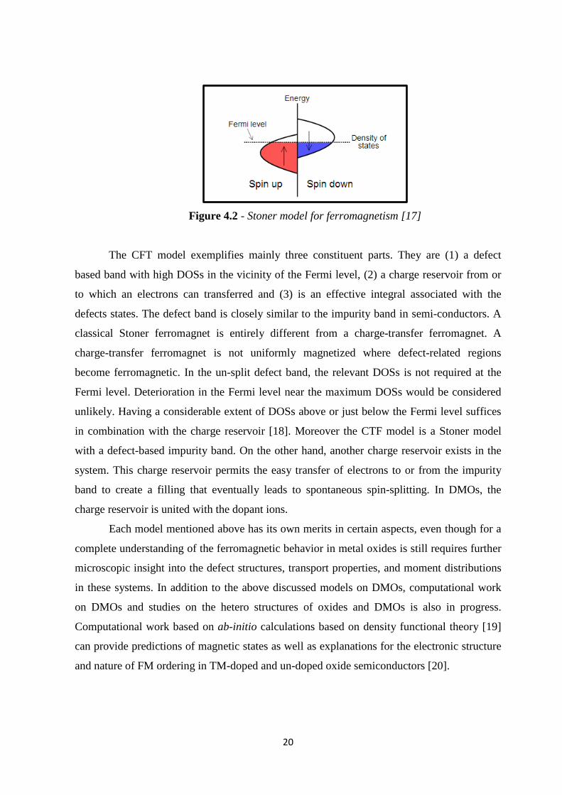
Figure 4.2 - Stoner model for ferromagnetism [17]
The CFT model exemplifies mainly three constituent parts. They are (1) a defect
based band with high DOSs in the vicinity of the Fermi level, (2) a charge reservoir from or
to which an electrons can transferred and (3) is an effective integral associated with the
defects states. The defect band is closely similar to the impurity band in semi-conductors. A
classical Stoner ferromagnet is entirely different from a charge-transfer ferromagnet. A
charge-transfer ferromagnet is not uniformly magnetized where defect-related regions
become ferromagnetic. In the un-split defect band, the relevant DOSs is not required at the
Fermi level. Deterioration in the Fermi level near the maximum DOSs would be considered
unlikely. Having a considerable extent of DOSs above or just below the Fermi level suffices
in combination with the charge reservoir [18]. Moreover the CTF model is a Stoner model
with a defect-based impurity band. On the other hand, another charge reservoir exists in the
system. This charge reservoir permits the easy transfer of electrons to or from the impurity
band to create a filling that eventually leads to spontaneous spin-splitting. In DMOs, the
charge reservoir is united with the dopant ions.
Each model mentioned above has its own merits in certain aspects, even though for a
complete understanding of the ferromagnetic behavior in metal oxides is still requires further
microscopic insight into the defect structures, transport properties, and moment distributions
in these systems. In addition to the above discussed models on DMOs, computational work
on DMOs and studies on the hetero structures of oxides and DMOs is also in progress.
Computational work based on ab-initio calculations based on density functional theory [19]
can provide predictions of magnetic states as well as explanations for the electronic structure
and nature of FM ordering in TM-doped and un-doped oxide semiconductors [20].

21
4.3 Ferro-Magnetism in un-doped metal oxides: d0–magnetism
Recent experimental results reported RTFM in wide-band gap oxides even without
the inclusion of magnetic atoms, which is called the d0 magnetism. In general d0 magnets are
a type of magnetic materials without any magnetic dopant and this type of material are
diamagnetic in their bulk form. This type of phenomenon was first reported by Coey et al. for
HfO2 [4]. Observation of ferromagnetism in these undoped systems invoked great excitement
and open wide debate as to the origin of magnetism in a semiconductor. Sundaresan et.al’s
[2] studies based on the nano particles of 7–30 nm diameter of nonmagnetic oxides such as
CeO2, Al2O3, ZnO, In2O2 and SnO2 argued that the RTFM is a universal characteristic of
nanoparticles of metal oxides. On the other hand, they observed that the bulk samples became
diamagnetic that obtained by the sintering of nanoparticles at high temperatures in air or
oxygen. They assumed that the origin of ferromagnetism may be the exchange interactions
between localized electron spin moments resulting from oxygen vacancies at the surfaces of
nanoparticles.
Theoretically, Elfimo et al. [21] suggested that the cation vacancy in oxides could
induce a local magnetic moment and contribute to the collective magnetism of materials.
Recently, Xing et al. [22] studies show that the strong correlation between the
ferromagnetism and the zinc vacancies and is confirmed by first-principles density functional
theory calculations. Also, the theoretical predictions and calculations carried out for the rock-
salt structured materials, such as CaO and MgO, indicating that the cation vacancy induced
magnetic moment [20- 23]. One of the general and common factors in all these type of oxide
materials is the presence of different types of defects such as atomic vacancies and
interstitials. Most of the experimental studies introduced dopant (for e.g. C or N) into the
lattice to investigate the mechanism of d0 –magnetism.
All of these surprising results have encouraged us to verify experimentally the
magnetic properties of undoped insulating and doped semiconducting oxides. In this thesis,
we present the studies of magnetism for (i) MgO thin films; (ii) Mg doped ZnO thin films and
(ii) Mn doped MgO thin films under different ambient conditions.

22
4.4 References
[1] LI XiaoLi, QI ShiFei, J. F. Xian, Q. Z.Yong and XU XiaoHong, Science China, Vol.56 No.1, 111 (2013) [2] Sundaresan A, Bhargavi R, Rangarajan N, Siddesh U and Rao C N R, Phys. Rev. B 74 161306 (2006). [3] Xu Q, Schmidt H, Zhou S, Potzger K, Helm M, Hochmuth H, Lorenz M, Setzer A, Esquinazi P, Meinecke C and Grundmann M 2008 Appl. Phys. Lett. 92 082508. [4] Venkatesan M, Fitzgerald C B and Coey J M D 2004 Nature, 430 630. [5] Coey J M D, Venkatesan M, Stamenov P, Fitzegerald C B and Dorneles L S 2005 Phys. Rev. B 72 024450. [6] Yan Z, Ma Y, Wang D, Wang J, Gao Z, Wang L, Yu P and Song T 2008 Appl. Phys. Lett. 92 081911. [7] Gu B, Bulut N, Ziman T and Maekawa S 2009 Phys. Rev. B 79 024407. [8] Kapilashrami M, Xu J, Str¨om V, Rao K V and Belova L, Appl. Phys. Lett. 95, 0331042009. [9] Wang Q, Sun Q, Cheng G, Kawazoe Y and Jena P 2008 Phys. Rev. B 77 205411. [10] Hu J, Zhang Z, Zhao M, Qin H and Jiang M 2008 Appl. Phys.Lett.93 192503. [11] Osorio-Guill´en J, Lany S, Barabash S V and Zunger A 2006 Phys. Rev. Lett. 96 107203. [12] Zener C. Interaction between the d shells in the transition metals. Phys Rev, 1951, 81: 440–444. [13] T. Dietl, H. Ohno, F. Matsukura, J. Cibert, D. Ferrand, Science 287 (2000)1019-1022. [14] J. M. D.Coey, M.Venkatesan, C. B. Fitzgerald. Donor impurity band exchange in dilute ferromagnetic oxides. Nat Mater, 2005, 4: 173–179. [15] M. R. Oliver, J. O. Dimmock, A. L. McWhorter, and T. B. Reed, PHYSICAL REVIEW B VOLUME 5, NUMBEB 3 1 FEBRUARY 1972]. [16] J. M. D. Coey, K.Wongsaprom, J. Alaria and M.Venkatesan, J. Phys. D: Appl. Phys. 41 (2008) 134012. [17] http://en.wikipedia.org/wiki/File:Stoner_model_of_ferromagnetism.svg. [18] J. M. D. Coey, P. Stamenov, R. D. Gunning, M.Venkatesan and K. Paul, New Journal of Physics 12 (2010) 053025. [18] http://www.ch.ic.ac.uk/harrison/Teaching/DFT_NATO.pdf. [20] X. Zuo, S. D. Yoon, A.Yang, W. H.Duan, C.Vittoria, and V. G. Harris, JAP, 105, 07C508 (2009). [21] I. S. Elfimov, S. Yunoki and G. A. Sawatzky, Phys. Rev. Lett. 89. 216403. [22] G. Z. Xing, Y. H. Lu, Y. F. Tian, J. B. Yi,3 C. C. Lim,2 Y. F. Li,1 G. P. Li,1 D.D. Wang, B. Yao, J. Ding, Y. P. Feng, and T. Wu, AIP Advances 1, 022152 (2011). [23] S. Gallego, J. I. Beltran, J. Cerda and M. C. Munoz, J. Phys.: Condens. Matter17, L451- L457 (2005).

23
Chapter 5
Sample Preparations: Fabrication of Thin Films 5.1 Introduction
It is clear that no single fabrication technique is universally suitable for the
manufacturing of nanometer scale devices. The lithographic techniques such as atomic beam
holography, scanning probe lithography and electron beam lithography are the some of the
preferred methods used to fabricate some devices and non-lithographic techniques are also
used for the fabrication of nano-devices [1-3]. Lithographic technique is a printing method
that uses chemical process to make an image. Basically, there are two types of lithographic
methods used in silicon industry, such as photolithography and e-beam (electron-beam)
lithography. Photolithographic process uses light to transfer a geometric pattern from a
photomask to a photo resist, a light sensitive chemical, on the substrate. Depending on the
decorative design on the photomask, we can produce different patterns on the substrate. This
technique is further used to make different Si based photonic and electronic devices [2, 3].
Non-lithographic techniques are based on the self-organization process. Generally,
this technique can be classified in to two, solution based deposition and vacuum based
deposition process. The solution based deposition process is based on the chemical reactions
in liquid phase. Examples of this technique are wet chemical synthesis such as spray
pyrolysis, spin coating, chemical bath deposition, vapour-liquid-solid method, etc. On the
other hand, the vacuum based deposition process takes place under high vacuum (~ 10-5 to
10-10 mbar) so that the technique is very clean and probability of deposition of impurity
materials is very low. Therefore, these types of process are highly desirable for device
fabrication. Examples of these types of deposition process are chemical vapour deposition
(CVD), laser ablation, molecular beam epitaxy (MBE), evaporation, sputtering, plasma arc
method, etc. Among these deposition techniques, sputtering is widely used in the
semiconductor industry to deposit thin films of different materials in integrated circuits (ICs)
processing. In optical applications, thin anti reflection coatings on glass are also deposited by
sputtering technique. This technique is an ideal method to deposit contact metals for thin film
transistors. It is also used to fabricate photovoltaic thin films for solar cells, thin film sensors,
metal cantilevers and interconnects etc [1-3].
Chemical vapor deposition (CVD) and physical vapor deposition (PVD) are the two
most general methods for transferring material atom from one or more sources to the growth
surface of a film being deposited onto a substrate. Vapor deposition describes any process in

24
which a solid immersed in a vapor becomes larger in mass due to transference of material
from the vapor onto the solid surface. The deposition is normally carried out in a vacuum
chamber to enable control of the vapor composition. If the vapor is created by physical means
without a chemical reaction then the process is said to be PVD, and if the material deposited
is the product of a chemical reaction then the process is called as CVD [3].
5.2 Sample Preparations: sputtering
We have prepared thin films by using reactive magnetron sputtering techniques. This
is one of the well-developed and sophisticated technique by which we can fabricate thin films
from both conducting (metal) and non-conducting (ceramic) targets [4-17]. Magnetron
sputtering can be done by either DC or RF modes. Usually on an industrial scale the film
fabrication is carried out by magnetron sputtering.
Figure 5.1 - A schematic representation of sputtering process at the Molecular Level.
5.2.1 Theory of Sputtering
Sputtering is one kind of physical vapour deposition and is commonly used for thin-
film deposition. This is a process whereby atoms in a solid target material are ejected into the
gas phase due to the bombardment of the material by energetic particles [1, 3]. Grove
founded the sputtering deposition technique in 1852 and this method is well developed and
applied to industry during last 200 years and lasting to modern time. Standard physical
sputtering process is carried out by the momentum exchange between the ions and atoms in
the material, due to collisions. In sputtering process, plasma of non-reactive ions, for e.g. Ar,
is created by a potential difference inside a vacuum chamber, which falls on the target
material and breaks the atoms and then collected on the surface to be coated (substrate).
According to momentum transfer theory, the incident particles cannot directly emit atoms

25
from the solid target surface, yet the momentum of the incident particles would be transferred
to the atoms near the conflict site, and in the meantime collisions along the crystal lattice will
be carried out in all directions, this causes random collisions along the crystal lattice. In this
way the surface atoms will get plenty of energy from the neighboring atoms. Eventually, the
atom gets energy greater than that of the binding energy, and then the atoms will be moved
out from the target surface. A schematic representation of sputtering process has been shown
in figure 5.1 [18].
To initiate sputtering, a high voltage is applied on the electrodes (cathode and anode);
the cathode is used as the source of the sputtered particles whereas anode is usually substrate
holder. When a negative charge is applied to the target material, the gas in between the
electrodes will break down and creates plasma. The positively charged gas ions generated in
the plasma are attracted towards the negatively biased target plate, i.e. cathode, at a very high
speed and starts sputtering process. The collision between positively charged gas ions and the
target plate creates a momentum transfer and ejects atomic size particles from the target.
These particles are deposited on to the surface of the substrates. During the sputtering
process, in addition to target atoms, secondary electrons are also ejected from the target
surface. These electrons will be accelerated towards the anode, and then the electrons would
collide with neutral gas atoms and form ions, according to the formula,
Ar + e−→Ar+ + 2e− --------------------------------- (1)
During this ionization process, charge conversion indicates that two electrons are
released. These two electrons will continue to form additional gas ions and electrons and so
on [19].
General sputtering techniques have two disadvantages. They are low deposition rate
and greater heating of the substrate due to the bombardment by the secondary electrons from
the targets. Magnetron sputtering was developed as a solution for these difficulties. By
introducing a magnetic field to restrict these electrons to region very close to the target
surface so that the heating effect of the substrate is reduced and the plasma is strengthen,
leading to high deposition rates. This type of deposition is called magnetron sputtering. This
type of magnetron sputtering is used where high deposition rate and low substrate
temperature is required.
5.2.2 Magnetron Sputtering
This technique is powerful and flexible PVD coating method and can be used to
deposit a wide range of materials such as metal, alloy and a variety of compounds. Prior to
26
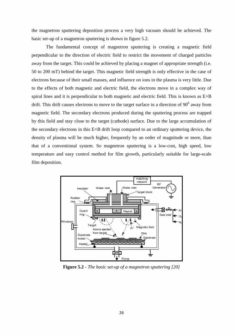
the magnetron sputtering deposition process a very high vacuum should be achieved. The
basic set-up of a magnetron sputtering is shown in figure 5.2.
The fundamental concept of magnetron sputtering is creating a magnetic field
perpendicular to the direction of electric field to restrict the movement of charged particles
away from the target. This could be achieved by placing a magnet of appropriate strength (i.e.
50 to 200 mT) behind the target. This magnetic field strength is only effective in the case of
electrons because of their small masses, and influence on ions in the plasma is very little. Due
to the effects of both magnetic and electric field, the electrons move in a complex way of
spiral lines and it is perpendicular to both magnetic and electric field. This is known as E×B
drift. This drift causes electrons to move to the target surface in a direction of 900 away from
magnetic field. The secondary electrons produced during the sputtering process are trapped
by this field and stay close to the target (cathode) surface. Due to the large accumulation of
the secondary electrons in this E×B drift loop compared to an ordinary sputtering device, the
density of plasma will be much higher, frequently by an order of magnitude or more, than
that of a conventional system. So magnetron sputtering is a low-cost, high speed, low
temperature and easy control method for film growth, particularly suitable for large-scale
film deposition.
Figure 5.2 - The basic set-up of a magnetron sputtering [20]

27
5.2.3 Balanced/Unbalanced Magnetron Sputtering
Figure 5.3 - (a) Balanced and (b) unbalanced magnetron sputtering [21]
In the case of usual magnetron sputtering system, the plasma is confined near the
target surface (figure 5.3a); however, it may not be always desirable. If the substrate is too
long from the target surface, due to very weak plasma results a low deposition rate and even
no deposition. So in certain cases this problem can be sort out by selective strengthening of
the magnetic field at the target, called un-balanced magnetron sputtering (figure 5.3b). In this
type of sputtering set-up, magnetic field lines in the centre and periphery of the target are not
totally closed loops. The magnetic field lines near the target surface maintains closed spiral
loops, so that to achieve the high deposition rate and part of the outside magnetic field lines
extend to the substrate surface. As a result, some part of the secondary electrons can reach the
substrate surface along the magnetic field lines, and plasma is no longer limited to target
areas so that ion current density on the substrate surface increased up to 10 mA/ cm2, and thus
improves deposition rate [19].
5.2.4 RF/DC sputtering
Normally there are two modes of power supplies, i.e. RF and DC power can be used
to initiate the discharges. In an RF sputtering system, a high frequency generator (13.56
MHz) is connected between the cathode and anode, with RF power via an impedance
matching network. In a DC sputtering system, a direct voltage is applied in between the
electrodes. The RF sputtering is suitable for both conducting and insulating targets. However
DC mode is used to sputter conducting materials, because if the target (cathode) is non-
conducting or insulator the accumulation of too much positive charge build up on the material
and finally the cathode will prevent any more positive gas ions to go to the target and it will

28
cease sputtering. To solve this problem, radio frequency (RF) sputtering technique is
introduced for non-conductive targets.
Figure 5.4 - Images of DC plasma (KTH-tmfy-mse)
The impedance of insulating or oxide targets materials decreases abruptly with
increasing frequency. Hence high frequency power is needed to pass current through the
dielectric target in order to create a discharge for the plasma. During this RF sputtering
process, a high-frequency voltage (above 50 kHz) is applied to the target. Consequently the
electric field in the plasma changes its polarity in that high frequency. In the negative half
cycle, positive ions bombard the target and are adsorbed on the target surface and in the
positive half cycle, due to more rapid mobility of secondary electrons than that of ions. These
secondary electrons can fly towards the target surface with in a short interval of time and
neutralize the positive ions on the target surface. In the meanwhile, a large number of
electrons heap up on the target surface to attract positive gas ions to bombard the target
continuously, so by using RF technique, sputtering of the insulator target could be achieved.
That is why an RF power supply is used in the sputtering of insulating targets [22]. Figure 5.4
shows the images of DC sputtering plasma generated inside a deposition chamber.
5.2.5 Thin film growth modes
There are three classical thin film growth modes. They are (i) Volmer-Weber, VW
(island); (ii)Frank-van der Merwe, F-M (layer by layer); and (iii) Stranski-Krastanov, S-K
(layer plus island/mixing) mode. The schematic representations of these modes are given in
figure 5.5.

29
Figure 5.5 - (a) Volmer-Weber (island) mode, (b) Frank-van der Merwe, F-M (layer by
layer) mode and (c) Stranski-Krastanov, S-K (layer plus island/mixing) mode [2]
Generally the thin films grown by sputtering technique are with island (V-W) growth
(Figure V.6). This VW mode consists in first phase of larger number of surface nuclei and in
second phase of their spreading. It means that the atoms/ molecules deposited on the surface
of the substrate are accumulated as a cluster. A cluster with enough number of atoms are
called critical nucleus will continue to absorb new atoms and makes itself to grow to form
island. During the deposition process these islands continues to keep on growing and further
develop into network structure. The vacant spaces in between this network will be packed
and finally forms a continuous film [23].
During layer by layer (F-M) mode a new layer is nucleated only after the completion
of the layer below and so on. This growth occurs over long distances in ideal cases. On the
other hand, crystals formed by this mode are not perfect and contain defects like dislocations.
Layer plus island/mixing (S-K) mode is considered as the intermediate between the two types
of growth mode mentioned above. Usually S-K mode starts as layer by layer growth and after
a few layers it turns out to island growth. This is due to the consequences of the lattice
mismatch from film and substrate. The lattice misfit between the film and substrate creates a
strain as a result of the increasing elastic energy with increasing layer thickness [24].
5.2.6 Deposition rate and Sputtering yield
The deposition rate at which a material is deposited at the substrate (anode) surface is
directly proportional to the rate at which it is detached from the target (cathode) [1]. The rate
may be represented by the relation
D = KIα ---------------------- (2)
Where D is the deposition rate, K is a constant which characterizes the sputtering
apparatus and α is the sputtering yield. Also α, the sputtering yield is a function of the

30
sputtering voltage and the particular ion being used and is defined as the number of atoms
ejected per incident ion. The sputter yield α is provided by the following equation:
α = (atoms removed)/ (incident ions) ----------------------------------- (3)
The sputtering yield determines the deposition rate and it depends on the following
factors; incident ion's energy, mass of bombarding ions, target material, incidence angle,
mass of bombarding ions, pressure and target structure.
Comparable to other deposition technique sputtering is one of the most versatile
techniques used for the fabrication of device–quality films. Sputtering process can able to
produce films with high quality, purity and better controlled composition. Originally, this
technique was used to fabricate thin films of metal, but later, compound materials (ceramics,
oxide materials, etc.) are also fabricated by this method. By using a sputtering system, we can
fabricate high quality films on different substrates such as single crystal substrates like Si,
sapphire, ZnO etc. and also non-crystalline substrates like glass, organic materials etc..
Generally speaking, magnetron sputtering has a number of advantages with other deposition
techniques [1, 3, 20]. They are (l) lower substrate temperature, (2) high deposition rate, (3)
good substrate-film adhesion and able to prepare uniform and homogeneous films on even
very large area, (4) easy control of deposition process and easy to adjust various parameters,
(5) simple equipment and relatively low cost, thus suitable for mass production. Especially,
substrate temperature and deposition time are the most suitable and beneficial elements for
the deposition of nanostructured materials on different substrates. Low deposition time is
required to obstruct the deposition of large number of particles to retain their nanostructure
and also decrease the probability of the particles to accumulate into bigger clusters. Low
substrate temperature is also prevents the accumulation of particles to remain in
nanocrystalline form.
For our studies we used a Leybold-Heraeus sputtering system-Combivac IT230.

31
5.3 References
[1] K.K. Chattopadhyay and A. N. Banerjee; Introduction to Nanoscience and Nanotechnology, Eastern Economy Edition (2009). [2] N. W. Parker, A. D. Brodie, J. H. McCoy, Microlithography World, 9 (2000). [3] L. B. Freund and S. Suresh; Thin FilmMaterials; Stress, Defect Formation and Surface Evolution, Cambridge (2003). [4] J. H.Jou M.Y. Han and D. J. Cheng, J.Appl.Phys. 1992,V-71, 4333(1992). [5] Y.E.Lee Y. E. Lee, J. B. Lee, Y. J. Kim, H. K. Yang, J. C. Parkand H. J. Kim, J.Vac.Sci.Technol.A.V-14, 1943 (1996). [6] X.Q.Meng et al., J.Appl.Phys.A.V-70,421 (2002). [7] C.Agashe et al., J.Appl.phys.V-95, 1911 (2004). [8] W.W.Wang et al., J.Thin.Sol.Fi.V-491, 54 (2005). [9] M.Jung et al., J.Cryst.Gr.V-283, 384 (2005). [10] D. Y. Ku, et al., Thin Solid Films, V-515, 1364 (2006). [11] Z.Y.Zhang et al., J.Cryst.Gr. V- 290, 341(2006). [12] D.Kim et al., J.PhysicaB. V-376, 741 (2006). [13] J.P.Zhang et al., J.Appl.Surf.S.V- 253, 9414 (2007). [14] Y.YKim et al., JPhysicaB. V-401,408 (2007). [15] G.Kiriakidis et al., J.Thin.Sol.Fi.,V-525, 8577 (2007). [16] V.Tvarozek et al., J.Thin.Sol.Fi.,V-515, 8756 (2007). [17] J.Wang et al., J.Thin.Sol.Fi.,V-515, 8780(2007). [18] http://www.unc.edu/~justink/RFDC_Sputtering.pdf. [19] Milton Ohring, ‘’Materials Science of Thin films, Deposition and Structure 2nd Edition, Academic Press (2002). [20] D. Song, Applied Surface Science, 254, 4171–4178 (2008). [21] http//www.advanced-energy.com. [22] KlasEllmer, J. Phys.D: Appl. Phys. 33, R17-R32 (2000). [23] Y. Kajikawa, Journal of Crystal Growth, 289, 387–394 (2006). [24] J. Palisaitis, R. Vasiliauskas, Physics of Advanced Materials Winter School 2008 (based on the lecture of Prof. Gabriel Ferro).

32

33
Chapter 6
Characterization Techniques 6.1 Introduction
When the dimensions of the materials are reduced to nanoscale, they show unique
properties which are entirely different from those of their bulk materials. For example, their
magnetic, optical and electronic properties change, their chemical properties can be
decreased/ increased and structural/ mechanical stabilities are changed dramatically. These
features make nano materials attractive for unique sensing applications, and also at the same
time cause complications in their characterization processes.
The tremendous advancement of material science, especially in nano structured
materials, is due to the discovery and development of most modern characterization tools.
Recently different characterization techniques are employed to know the crystal structure,
surface morphologies, thickness and purity of the films. The crystal structure of the films can
be characterized by X-ray diffraction (XRD) technique. A dual-Beam ultra-high resolution
(UHR) Scanning Electron Microscope (SEM)/Focused Ion Beam (FIB) is a useful technique
to determine the thickness of thin film. Generally, atomic force microscopy (AFM) is used to
getting the idea about surface morphologies of the thin films. The elemental mapping of the
films can be done using energy dispersive x-ray (EDAX)/X-ray photoelectron spectroscopy
(XPS) technique. In our experimental work, we have employed all of these modern
techniques to characterize our thin films. In addition to this, the magnetic properties of the
films were measured in a superconducting quantum interference device (SQUID)
magnetometer. Description of various characterization techniques are described in the
following sections.
6.2 X-ray diffraction (XRD)
X-ray diffraction (XRD) is a one class of non-destructive analytical technique used to
reveal the information about the chemical composition, identify phase and orientation,
determine structural properties, estimate the size of nanoparticles, etc. of natural and
fabricated thin film materials[1-2]. In XRD, X-rays are generated with in a sealed tube that is
under vacuum. A current is applied to the tube, which heats a filament within the tube and
emits electrons. The number of electrons emitted from the filament depends on the applied
current. The higher the current the greater the number of electrons emitted from the filament.
A high voltage (15-60kV) is applied within the tube and this voltage accelerates the electrons.
These accelerated electrons hit a target, made of copper (Cu), producing X-rays and

34
wavelength of these X-rays is the characteristic of that target. These X-rays are collimated
and focused onto the sample. A detector detects the X-ray signal and converting the signal to
a count rate [3].
Solid matter can be classified in to two groups. They are amorphous and crystalline
materials. Glasses are amorphous materials in which atoms are arranged in a random manner.
But in crystalline materials atoms are arranged in a periodic manner called a unit cell, which
is periodically repeated in three dimensions on a crystal lattice. The spacing between unit
cells in a different direction is called its lattice parameters. The dimension of the unit cell is
described by three axes named as a, b, c and the angles between them are alpha (α), beta (β)
and gamma (γ) [4]. When a focused X-ray beam interacts with the planes of atoms in the
sample, a part of the beam is transmitted, a part is absorbed by the sample, a part is refracted
and scattered, and a part is diffracted. Diffraction of X-ray beam by a crystalline material is
an analogous to diffraction of light by water drop-lets and producing the rainbow. X-rays are
diffracted by each material differently, depending on what atoms make up the crystal lattice
and how these atoms are arranged.
Figure 6.1 - The schematic representation of Bragg diffraction [5].
When an X-ray beam incident on a sample and is diffracted, by using Bragg’s law we
can measure the distances between the planes of the atoms that constitute the sample.
Consider a crystal is bombarded with X-ray beam with a fixed wavelength (λ) and is incident
on the lattice planes in the crystal at an angle (θ). When the wavelengths of the scattered x-
rays interfere constructively then intense reflected x-rays are produced. The interference will
only occur when the two rays are completely in phase whenever the differences in the travel
path should be equal to the integral multiple of λ. Due to this constructive interference, a

35
diffracted beam of X-rays will leave the crystal lattice plane at an angle equal to that of the
incident beam. The relationship between the wavelength of the incident X-rays (λ), angle of
incidence (θ) and the spacing between the crystal lattice planes of the atoms (d) is known as
Bragg’s law and is expressed as: nλ= 2dsinθ ----------------------- (4)
Where ‘n’ is an integer and is the order of the diffracted beam. Figure 6.1 shows the
schematic representation of Bragg diffraction. Almost 95% of all solid materials can be
described as crystalline materials. The d-spacing generated in a typical X-ray scanning
provides a unique finger print of the sample.
For a given XRD spectrum, the average crystal grain size (d) can be estimated using
the Scherrer formula [6] given by 0.9 180 ---------------------------(5)
cosd λ
β θ π=
where λ = 0.15405 nm, is the wavelength of the Cu Kα radiation and β is the full
width at half maximum (FWHM) of the diffraction peak from the (hkl) crystal plane.
Also from the XRD data, we can calculate the strain by using the Bragg’s equations,
nλ = 2dhklsinθ, where n is an integer, λ is the wavelength of incident wave, dhkl is the
crystalline surface distance for (h k l) indices, and θ is the angle between the incident ray and
the scattering planes. The lattice parameter can be calculated by the formula,
2 2 2 2 2
14( ) / 3 /
hkldh k hk a l c
=+ + +
-----------------------(6)
where a and c are the lattice parameters. From above equations for (002) plane, we
obtain the equation, c =λ / (sinθ). Therefore the strain along the c axis is given by the
equation
ε= (c-co)/co * 100%-------------------------(7)
where c is the lattice parameter of the strained ZnO films calculated from x-ray
diffraction data and co=5.207Å, is the value of the unstrained lattice parameter of ZnO [7].
For the studies of our samples, we used a
Siemens D5000 powder X-ray diffractometer.

36
6.3 Dual Beam Scanning Electron Microscopy (SEM)/Focused Ion Beam (FIB)
6.3.1 Scanning Electron Microscopy (SEM)
SEM is one type of electron microscope that images samples by a beam of high-
energy electrons. These high energy electrons interact with atoms by which the sample is
made up of and generating a variety of signals. The signals that formed by the interaction of
the electron and sample tells us the information about the sample such as chemical
composition, texture (external morphology), crystalline structure etc. The SEM has many
advantages over conventional microscopes. The SEM has a large depth of field and higher
resolution. This large depth field allows more of a specimen to be in focus at one time and
also closely spaced specimens can be magnified at much higher levels. The SEM uses
electromagnets instead of lenses so that researchers can control the degree of magnification.
Figure 6. 2 show the schematic representation of a SEM. The major components of all SEMs
include the following arrangements [8, 9].
I. Electron gun (source)
II. Electron lenses (including condenser lens and objective lens)
III. Scanning coil
IV. Sample chamber (Stage)
V. Detectors for all signals of interest
VI. Data output devices
VII. Infrastructure facilities such as power supply, vacuum system, cooling system,
vibration-free floor and room free of ambient electric and magnetic fields.
Figure 6. 2 Schematic representation of a SEM [10]

37
SEM produces magnified images by using electrons instead of light. The electron gun
produces a beam of electrons that follows a vertical path through the microscope, which is
kept in a vacuum. The electron gun consists of three components. They are (1) a filament
(cathode) made of various types of materials such as lanthanum hexaboride (LaB6) crystal,
tungsten wire or cerium hexaboride (CeB6). Among this the most common one is the
Tungsten hairpin gun. (2) A grid cap (Wehnelt cylinder), which controls the flow of
electrons. (3) A positively charged anode plate. A voltage is applied to the tungsten loop and
allows it to heat up to produce electrons. The anode plate, which is positive w.r.t cathode
(filament), that attracts and accelerates the electrons down to the sample. This electron beam
passes through electromagnetic fields and lenses, which focus the beam and allows hitting the
sample. Simultaneously X-rays and electrons are ejected from the sample (Figure 6. 3).
Detectors receive these X-rays, backscattered electrons and secondary electrons and finally
convert them into a signal that is sent to a screen. This produces the final image.
Figure 6. 3 The representation of ejection of X-rays and electrons from the sample [10]
In a SEM, the accelerated electrons carries enormous amount of kinetic energy (KE)
and allows them to hit the sample. When the incident electrons are decelerated in the solid
sample, this kinetic energy is dissipated into a variety of signals. These signals include
secondary electrons, backscattered electrons (BSE), diffracted backscattered electrons
(EBSD), visible light, X-rays and heat. These secondary electrons are used to produce SEM
images. The diffracted backscattered electrons are used to determine the crystal structures
and orientations of the samples. That is, the accelerated electrons in the SEM can be
diffracted by atomic layers in the crystalline materials and these diffracted electrons can be
detected when they hit on a phosphor screen and simultaneously produce visible lines. This is
called Kikuchi bands or electron backscatter patterns. These Kikuchi bands are the
projections of the geometry of the lattice planes in the crystal. This gives the exact
information about the crystallographic orientation and crystalline structure of the samples.
The BSE and secondary electrons are generally used for imaging. The secondary electrons

38
are most important for showing surface morphology and topography of the samples and the
BSE are most important for showing contrasts in multiphase samples. X-rays are produced
due to the inelastic collisions of the electrons with the electrons in the outer most orbitals of
the atoms of the sample. Due this collision, electrons in the sample moves to a higher energy
state (excited state). These excited electrons supply X-rays of fixed wavelength when they
return back to the lower energy states. The wavelength of the X-rays depends on the
difference in energy levels of electrons in different shells of a given element. Thus
characteristic X-rays are produced in each element that is excited by the electron beam. So
SEM analysis is considered to be a non-destructive analytical technique and it is possible to
analyze the sample repeatedly [11].
6.3.2 Focused Ion Beam (FIB)
Focused Ion Beam (FIB) system is versatile technique which enables for inspection,
characterization, structuring or manipulating a wide range of materials [12]. The basic
concept of FIB microscope is similar to SEM. FIB system uses charge atoms (ion) beam to
raster over the surface of a sample in a similar way as the electron beam in a SEM. Generally
in FIB system, a fine tungsten pin covered with liquid Gallium is used as an ion source. From
ion source, gallium atoms (Ga) are extracted and ionized via high tensions. This ionized Ga
atoms (Ga+) are accelerated in the ranges of 0.5 to 30 keV and focused on the sample with
the help of electrostatic lenses. The Ga+ hits the sample surface and sputters a small amount
of material and which leaves the surface as either as secondary electrons or neutral atoms.
Also the primary Ga+ beam produces secondary electrons or ions. These secondary electrons
or ions are collected to form an image of the sample surface. The ion beam can be used to
produce an image of the sample surface. Also it allows to milling of small holes on the
sample at well localized sites so that it is used as an excellent tool for making cross-sectional
images of the thin films for measuring thickness. Some of the important applications of FIB
include the following.
1. Cross-sectional analysis
2. Imaging modification of the electrical routing on semiconductor devices
3. Failure analysis
4. Micro-machining
5. Preparation of samples for Atom Probe analysis
6. Preparation of specimens for transmission electron microscopy (TEM). Etc.
Now-a-days most instruments combine both SEM and FIB systems together called
Dual beam or Multi beam or Cross beam system. By using these types of systems, one can do

39
both imaging and milling. Usually the electron beam is used for imaging and ion beam for
milling.
A dual beam SEM/FIB Nova 600 Nanolab (FEI Co.) is used for our studies.
6.4 Energy Dispersive X-ray spectroscopy (EDXS)
Energy Dispersive X-ray spectroscopy (EDXS, EDX or EDS) is an important
analytical technique which is used for performing elemental analysis or chemical
characterization of a sample. It is one of the variants of XRF and it is associated with the
electron microscope, e.g. scanning electron microscopy (SEM) and transmission electron
microscopy (TEM) and is not a surface science technique. This technique detects the X-ray
emitted from the sample after the bombardment of the electron beam to characterize the
elemental composition. Figure 6.4 shows the basic principle of EDXS.
Figure 6.4 - Principle of EDS [13]
When the sample is bombarded with a focused electron beam from the SEM, the
electrons are ejected from the atoms of the sample and this result in electron vacancy. These
vacancies are filled by the electrons from higher state and an X-ray is emitted to balance the
energy difference between the two states of the electrons. It means that, the incident beam of
the electrons may excite an electron in an inner shell of the atom, e.g. K shell, ejecting it from
the shell and creating an electron hole. An electron from the higher energy shell, e.g. L shell,
then fills the hole. The energy difference between these higher and lower energy levels will
be released in the form of an X-ray. The energy and the number of the X-rays emitted from a
sample can be measured by an EDXS instrument. Atomic structure of the elements is
different from one other and the energy of the X-rays are the characteristic of the energy

40
difference between the two shells of the atomic structure of the element from which they are
emitted, this allows the EDXS equipment to analyze the elements contained in the sample
[13,14].
For our studies we used an OXFORD D7021 attached to a high resolution Hitachi
3000N SEM.
6.5 Superconducting Quantum Interference Device (SQUID-MPMS)
Superconducting Quantum Interference Device (SQUID) is a most sensitive
magnetometer used to measure very feeble magnetic fields. This system is functioning on the
basis of two important properties of superconductors. They are flux quantization and the
Josephson Effect. The device is also used to detect current, voltage, inductance and magnetic
susceptibility etc.
There are two types of SQUID system, (i) RF and (ii) DC. RF SQUID consists of a
single Josephson junction inserted into a superconducting loop. This is also known as AC
SQUID and consists of only one Josephson junction, which measures the interactions
between the superconducting ring and an external resonant LC circuit. External inductor
induces current in SQUID ring, and when the Josephson junction enters the resistive state it
damps the LC circuit. Whereas the DC system consists of two parallel Josephson junctions,
which are made up of two superconducting loop separated by a thin insulating layer. During
the measurement process, the SQUID system does not measure magnetic field directly. A
measurement is accomplished in the SQUID-MPMS by the movement of the sample along
the axis of the superconducting detection coils, which are situated at the center of the magnet
and outside the sample chamber. By the movement of the sample through the coils, the
magnetic moment of the sample produces an electric current in the detection of coils. The
connecting wires, detection coils and the SQUID-MPMS’s input coils form a closed
superconducting loop. Due to the formation of the closed loop, any variations in the magnetic
flux in the detection coils produces corresponding variations in the persistent current in the
detection circuit and which is directly proportional to the change in magnetic flux. The
SQUID system functions as a highly linear current to voltage converter, i.e., any feeble
change in the current in the detection coils creates corresponding variations in the SQUID
output voltage and these are directly proportional to the magnetic moment of the sample [15].

41
Figure 6. 5 - A schematic diagram of the internal set up of the SQUID-MPMS [15].
Figure 6. 5 show a schematic diagram of the SQUID-MPMS. Generally a SQUID
system consists of mainly five components. They are (1) Temperature control system. It can
control the sample temperature from 1.7 to 350 K; (2) Magnetic field control system. It
controls the magnetic field in the SQUID from -1 to +1 Tesla; (3) SQUID superconducting
system; (4) Sample control system. It enables the sample to move smoothly through the
detection coils; and (5) Data collecting system. It collects data such as helium level,
temperature, external magnetic field, etc. For studying the temperature dependence of the
magnetization of our studies, field cooled magnetic moment (MFC) is recorded in a magnetic
field of 2 kOe and of remnant magnetic moment (Mrem) recorded after cooling the sample in 2
kOe and then switching off the magnetic field.
For our study, a SQUID MPMS system from Quantum Design, USA is used.
6.6 Ultra Violet-Visible near Infrared spectroscopy (UV-Vis NIR or UV/Vis NIR)
The estimation of the band gap of materials is important in the solar cell,
semiconductor and nanomaterial industries. The “band gap” refers to the difference in energy
between the valence band and the conduction band. Electrons are able to jump from one band
to the other. An electron requires a specific minimum amount of energy known as ‘‘band gap
energy’’ to transit from the valance band to conduction band. A diagram illustrating the band

42
gap is shown in Figure 6.6. The band gap of a material can be determined from its UV
absorption spectrum. UV-VIS spectrophotometry refers to the absorption or reflectance
spectroscopy in ultraviolet-visible spectral region, i.e., it uses light in the visible and near-UV
and near-infrared (NIR) ranges. The absorption in the visible range directly affects the
perceived color of the chemicals involved. In this region of the electromagnetic radiation,
molecules undergo electronic transitions. This UV-VIS NIR technique is complementary to
fluorescence spectroscopy. Fluorescence spectroscopy deals with the transitions from the
excited state to the ground state on the other hand the absorption measures transitions from
the ground state to the excited state.
Figure 6. 6 - Band gap-explanation [16]
Wide band gap materials are essential for making UV lasers and diodes. Energy is
absorbed in the ultra violet or visible region can causes a change in the electronic excitation
of the molecule, and results in corresponding change in its ability to absorb light in the uv-
visible region of the electromagnetic radiation. This leads to transition in colour. The
relationship between energy absorbed in an electronic transition and the frequency (υ),
wavelength (λ) and wave number (ῡ) of radiation producing the transition is given by
(8)hcE h h cυ υλ
−
∆ = = = − − − − − − − − − −
Where h is Planck’s constant, c is the velocity of light and ΔE is the energy absorbed
in an electronic transition in a molecule from lower energy level (ground state) to higher
energy level (excited state). The absorbed energy depends on the difference in energy
between lower and higher energy level and the energy difference is inversely proportional to
the wavelength of the absorption. The fundamental characteristics of an absorption bands are
the intensity and position. The position of an absorption band corresponds to the wavelength
of radiation whose energy is equal to that required for an electronic transition. The intensity
of absorption bands depends on two factors. They are (1) the probability of the interaction

43
between the radiation energy and the electronic system and (2) the difference between the
ground state and excited states. The intensity of absorption is derived from Beer-Lambert’s
law A clε= , where ‘A’ is the measured absorbance, ‘ε’ is the proportionality constant called
molar absorptivity, ‘l’ is the path length (i.e., the distance traveled by the light through the
material) of the cell and ‘c’ is the concentration or number density of absorbers [17, 18].
UV-Vis Spectroscopy is a powerful tool for the characterization of semiconductor
materials. Optical absorption features of semiconductor can be explained on the basis of
excitation of the valence shell electrons to the conduction band, creating an electron-hole pair
in the system. Theoretical energy band gap of the Mg doped ZnO films was evaluated using
the Tauc’s relation [19] given by
( ) ( )ngh D h Eα ν ν= − ----------------------(9)
Where D is a constant, hν is the incident photon energy, Eg is the optical energy band
gap, and α is the absorption coefficient. Here α = -ln(T)/d, where T is transmittance and d is
the thickness of the thin film. The exponent n depends upon the type of optical transition in
the material. In case of the ZnO, n is equal to ½ for direct allowed transitions.
For our studies, the measurements were performed on JASCO-V-570 UV-vis-NIR
spectrophotometer operated at a resolution of 1 nm.
6.7 The near-edge x-ray absorption fine structure (NEXAFS)
Over the last decades, the spectroscopic studies based on synchrotron techniques have
contributed significantly for the better understanding of the properties of materials on the
microscopic and macroscopic scale. These techniques can be applied to samples from a
variety of fields, such as Materials Science, Life Sciences, Biology and Chemistry. Among
them, one of these techniques is NEXAFS spectroscopy. It is an element specific technique,
revealing the charge state, local environment, electronic structure, information on the
orientation of adsorbed molecules, hybridization etc of specific cations present in the material
[20, 21].
Figure 6.7 - Schematic representation of the basic theory of NEXAFS [22]

44
NEXAFS is a relatively young technique compared to other types of X-ray absorption
spectroscopy. It examines thoroughly the absorption of electromagnetic radiation by
excitation of core electrons into unoccupied bound or continuum states. The NEXAFS
exhibits the distinctive features in the energy region just below and up to about 50 eV above
the absorption edge (e.g. K-edge) [21]. The working principle of an NEXAFS involves the
excitation of electrons from an innermost level to partially filled or empty states. The
sample’s atom absorbs an X-ray photon and emits a core electron from the K (1s) or L (2p)
shell. This electron propagates outwards to an unoccupied discrete level and thereby creating
a core hole. An electron from a higher energy level fills the hole and releasing excess energy
either by the radiation of fluorescence photons or by the emission of Auger electrons (Figure
6.7). So, the shape of the spectral line and peak positions in a NEXAFS spectrum are directly
related to the nature of these unoccupied electronic states. The core holes may also decay via
the emission of fluorescent photons and which arises from the top 200 nm of the film as
opposed to Auger electrons, which originate from the top 10 nm. Consequently, this
technique is both surface and bulksensitive and is capable of probing thin films. NEXAFS
spectra are recorded by measuring either the fluorescence yield or electron yield as a function
of incident photon energy [22].
For our studies, NEXAFS experiments were performed on
BL7 at the advanced light source (ALS, USA).
6.8 Atomic Force Microscopy (AFM)
Atomic force microscopy is one of a family of Scanning Probe Microscopy (SPM).
The AFM was invented by Binning Et al. in 1986. This type of microscopes work by
measuring a local property, such as height, optical absorption and magnetism, with a tip or
probe kept very close to the specimen. AFM measures topography of surface of the sample
with a force probe. A fine probe is connected to the free end of a cantilever and it is brought
to very close to the sample surface and it measures the attractive or repulsive forces acting
between a fine tip and a sample. These attractive or repulsive will cause a positive or negative
bending of the cantilever and the bending is detected by means of a laser beam, which is
reflected from the back side of the cantilever [11, 23]. Figure 6.8 shows the basic concept of
AFM.
Major Components of an AFM
The major components of an AFM are piezocrystals and probe. In addition to this, an
optical detection system and electronics are necessary for the scanning procedures and data

45
acquisition. Piezocrystals are a class of ceramic substances that can expand or contract in the
presence of voltage gradient and vice versa. Piezocrystals develop an electrical potential in
response to mechanical pressure. In this way, it can be able to move in x, y and z directions.
The probe represents a sharp tip mounted on a soft cantilever and is interacting with the
sample surface. Each probe has its own specifications and shape. Generally, V-shaped
cantilevers are popular. The dimension of the cantilevers ranges from 100 to 200 μm in
length, 10 to 40 μm in width, 0.3 to 0.02 μm in thickness and the range of radius of curvature
at the end of the tip is 5 to 30 nm. Usually cantilevers are made from silicon (Si) or silicon
nitride (Si3N4). Today most of the AFMs use a laser beam deflection system to measure the
displacement of the cantilever. This system offers a sensitive and convenient method of
measuring the displacement of the cantilever. In this system a laser is reflected from the back
side of the AFM cantilever and allows collecting in a photodiode as shown in figure 6.8.
Figure 6.8 - (a&b) the basic concept of AFM.
In an AFM, a force sensor can work only if the cantilever probe interacts with the
force associated with the surface of the sample. The dominant short-range interactive force
associated with the AFM is van der Waals (VdW) interactions. However long-range
interactions, such as electrostatic, magnetic, capillary etc., are farther away from the surface
and are significant in other SPM techniques [11]. Figure 6.9 shows the interatomic force, i.e.
VdW force, up on probe distance from the sample.

46
Figure 6.9 - the inter-atomic force as a function of probe-sample separation.
AFM-Operation Modes
The AFM can be operated in three different modes, contact, non-contact and tapping
mode (intermittent contact mode) [23, 24], see figure 6.9.
i. Contact Mode: - In the contact mode, an AFM cantilever tip makes a feeble
physical contact with the sample surface. According to Hooke’s law, the displacement (Δx)
of the cantilever is directly proportional to the force (F) acting on the tip, i.e.
F= -k. Δx ------------------------------------ (6)
where ‘k’ is the spring constant of the cantilever. The cantilever bends, when the spring
constant of the cantilever is less than that of the surface of the sample.
In this operation mode the tip is either scans at a fixed height above the surface of the
sample or under the conditions of fixed force in order to obtain a uniform cantilever
deflection. As the scanner gently drags the tip over the surface of the sample, the detection
system measures the vertical deflection of the cantilever; this indicates the local sample
height. Thus, by using this mode the AFM system measures the hard-sphere repulsive forces
between the tip and the sample surface. Some of the advantages and disadvantages of this
mode are given below.
Advantages: 1. fast scanning; 2. used for friction analysis; 3. better for the analysis of
rough samples; Disadvantages: The Van der Waals forces can damage or deform soft
samples; however this problem can be resolved by the imaging of samples in liquids.
ii. Non-contact Mode: - In this mode, AFM cantilever operates in the attractive force
region and the interaction between the tip and the sample is minimized. In this mode of
operation the cantilever is allow to vibrate above the adsorbed fluid layer on the surface of a

47
sample and the AFM derives the topographic images from the measurements of attractive
forces. This mode is used for studying soft or elastic samples. Some of the advantages and
disadvantages of this mode are given below.
Advantages: Low force is exerted on the sample due to the minimization of the
interaction between the tip and the sample. This extends the probe’s lifetime; Disadvantages:
The resolution is low and the contaminant layer on the surface of the sample can take part
with the vibration. It usually requires ultra-high vacuum (UHV) for getting good images.
iii. Intermittent Mode: - This technique is similar to the contact mode. In this mode
the rigid cantilever is oscillated at it resonant frequency near to the sample surface. During
the scanning a part of the oscillation goes to repulsive mode, so that the probe is
intermittently touches or taps the sample surface. A constant tip-sample interaction can be
maintained by a constant to and fro motion of the cantilever and result to get images. This
technique has its own the advantages and disadvantages and given below.
Advantages: This allows high resolution of samples loosely held to surface so it is
good for the analysis of biological samples; Disadvantages: It is very difficult to image in
liquids, for this slower scanning speed is required.
In the present study we used a Dimension 3100 from Veeco and a MFP 3Dfrom Asylum research.
6.9 Mini Infrared Lamp Heating System (MILA) ULVAC- RIKO: MILA-5000
Rapid Thermal Processing (RTP) is an important heating technique for annealing
ferroelectrics, semiconductors and other thin film devices. But until now, only large and
expensive production systems are available for this rapid heating/cooling technique, making
lab work difficult, especially on small samples. To rectify these difficulties, ULVAC has
developed the MILA-5000 Mini Lamp Annealer. This instrument is highly sophisticated and
compact table top RTP system, built around a gold reflector IR furnace equipped with a high
precision temperature controller. The furnace uses a heating system, in which a near/far-
infrared lamp is fixed at the focus of the paraboloidal reflector and reflects infrared beams in
parallel onto a quartz sample stage of 20 mm X 20 mm. Being sealed in a quartz glass tube,
these infrared lamps generate no gas from the heating element and allow clean heating. The
body of the furnace is made of aluminum (Al) and is cooled with water to allow heating to a
high temperature. It has a wide range of available heating rates, and depending on the type of
thermocouple used, it can be used for annealing up to 1200°C [25].
For our studies we used a Mini Infrared Lamp Heating System ULVAC- RIKO: Model MILA-5000

48
Figure 6.10 - Schematic views of the experimental procedures.
PREPARED SAMPLES
IR-Annealer For Annealing
Magnetic Properties
SQUID-MPMS
XRD, AFM, SEM, EDS, FIB…
Structural, Surface morphologies, Elemental composition, Thickness.......
Optical Properties (Band-gap Studies)
UV-VIS ABSORPTION
Electronic Structure
NEXAFS
ANALYSIS OF THE OBTAINED DATA
CHARACTERIZATION (AS- GROWN AND ANNEALED)
PREPARATION OF SAMPLES BY
RF/DC SPUTTERING

49
6. 10 References
[1] P.Scherrer, GöttingerNachrichten Gesell, V-2, 98(1918). [2] W.L.Bragg, Proceedings of the Cambridge Philosophical Society, V-17, 43 (1913). [3] http://www.bccmeteorites.com/XRD.PDF. [4] http://epswww.unm.edu/xrd/xrdbasics.pdf. [5] http://scientificsentence.net/Waves/index.php?key=yes&Integer=bragg. [6] K. P. Misra, R. K. Shukla, A. Srivastava, and A. Srivastava, App. Phys. Lett. 95, 031901 (2009). [7] M. K. Puchert, P. Y. Timbrell, and R. N. Lamb, J. Vac. Sci. Technol.A 14, 2220 (1996). [8] http://science.howstuffworks.com/scanning-electron-microscope2.htm [9] https://imf.ucmerced.edu/downloads/semmanual.pdf [10]http://www.purdue.edu/rem/rs/sem.htm#1 [11] K.K. Chattopadhyay and A. N. Banerjee; Introduction to Nanoscience and Nanotechnology, Eastern Economy Edition (2009). [12] C. A. Volkert and A. M. Minor, Focused Ion Beam Microscopy and Micromachining, MRS Bulletin / Volume 32 / Issue 05 / May 2007 [13] http://de.wikipedia.org/wiki/Augerelektronenspektroskopie [14] Yan Wu, KTH, Doctoral thesis, 2010 [15] Mike McElfresh, ‘‘Fundamentals of magnetism and magnetic measurements’’, Quantum Design Inc, SanDiego, California (1994). [16] http://en.wikipedia.org/wiki/Band_gap [17] http://shodhganga.inflibnet.ac.in/bitstream/10603/369/13/13_chapter5.pdf [18] Usha Raghavan, Ph. D. Thesis, University of Pune 2012 [19] J. Tauc, 1974, Amorphous and liquid semiconductors, Chapter 4, ed. by J. Tauc, Plenum, London [20] A. P. Singh, R. Kumar, P. Thakur, N. B. Brookes, K. H. Chae and W. K. Choi, J. Phys.: Condens. Matter 21, 185005 (2009). [21] G. Hähner, Chem. Soc. Rev., 35, 1244, (2006). [22] T. H. Benny, S. Banerjee, S. Sambasivan, M. Balasubramanian, D. A. Fischer, G. Eres, A. A. Puretzky, D. B. Geohegan, D. H. Lowndes, W. Han, J. A. Misewich, and S. S. Wong, Small, 2, No. 1, 26 (2006). [23] Introduction to Scanning Probe Microscopy (SPM); Basic Theory: Atomic Force Microscopy (AFM); R. A. Wilson; H. A. Bullen, Department of Chemistry, Northern Kentucky University, Highland Heights, KY 41099. [24] http://www.nanoscience.com/education/afm.html [25] http://mediaserver.voxtechnologies.com/FileCache/ULVA-MILA-5000-Series- datasheet-2456983841.pdf

50

51
CHAPTER 7
RESULTS AND DISCUSSIONS 7.1. Comparative study of room temperature ferromagnetism in MgO films deposited
by sputtering Mg and MgO targets (Supplement II)
PROTOCOL 1: Fabrication of MgO films from Mg and MgO targets.
MgO films were prepared on glass and Si substrates by sputtering Mg (purity:
99.99%) and MgO (purity: 99.99%) targets at room temperature, respectively. The glass and
etched Si substrates were cleaned by conventional methods. The vacuum chamber was
evacuated to ~10-6 mbar. Prior to the film growth, the targets were cleaned by sputtering them
for 30min. Mg target was sputtered in the nitrogen(N2) and Oxygen (O2), whereas MgO
target was sputtered in Ar and O2. In both case the oxygen partial pressure was 1.3 × 10⁻⁴
mbar was maintained in the chamber with a total pressure of 3 × 10⁻³mbar. The films from
Mg and MgO targets were deposited with the DC power of ~ 60W and RF power of ~200W,
respectively.
Result and Discussions 1:
Figure 1 - XRD pattern of MgO thin films deposited on glass by sputtering (a) Mg and
(b)MgO targets for different times: 60,120 and 180min.
Figure1. shows the XRD patterns of the films deposited on glass from Mg and MgO
targets for different deposition times. For the MgO films deposited from Mg target, the broad
peaks corresponding to MgO (200) were detected, as shown in Figure1 (a), indicating the
significant fraction of amorphous component in the films. This peak broadening could be
caused by the non-uniform strain within the films. However, MgO films deposited from MgO
target are oriented along (200) axis [Figure 1 (b)], revealing the films deposited from MgO

52
target are more crystalline. The peaks are shifted towards the lower angle compared to (200)
peak of MgO bulk material, which is at about 42.92o (JCP2.2CA:00-045-0946). The shifting
could be caused by the uniform strain within the films. The strain of the films may arise for
the two reasons. One is the lattice mismatch between material and substrate and the other one
is intrinsic defects in the film. In our experiments, the MgO films were deposited on glass or
Si substrates under the same conditions. Therefore, the strain due to lattice mismatch should
be of same level for the films on the same type substrate. Thus, the variation of strain in the
films was caused predominantly by the variation of defect concentration [1].
The thickness of the films was in the range of 21-432nm. All films were found to be a
regular uniform surface, with no obvious punctures, as judged from cross-section analyses
using FIB. AFM was performed to investigate the surface microstructure of the samples.
Figure 2 shows the typical AFM images of MgO thin films deposited from Mg and MgO
targets, indicating that the films were composed of globe-like grains. Obviously, the grain
size of MgO films from MgO target was larger than that of MgO films from Mg target.
Figure 2 - AFM morphologies of MgO thin films deposited at the working pressure of
3×10 -3mBar: (a) from Mg target and (b) from MgO targets, two pictures are
taken in different magnifications.
The magnetic field dependence of magnetization (M-H) of the samples was studied at
room temperature. All of MgO films show room temperature ferromagnetism. Figure 3 shows
the M-H full loops for the samples deposited with the deposition time of 60 and 120min from
MgO and Mg targets.

53
Figure 3 - The M-H curves at 300 K for the thin films deposited for 60 and 120min from Mg
target after correcting diamagnetic components. Insets: M-H loops of the samples
deposited from MgO target under the same conditions.
Figure 4 - Comparison of MS values with thickness of MgO films prepared from Mg and MgO
targets
In this study, we compared the room temperature ferromagnetism of MgO films
prepared by sputtering Mg and MgO targets. From figures 4, it can be seen that the saturation
magnetization (Ms) of the films increases at first as the film’s thickness increases and then
decreases. It means that the magnetism as a function of increasing the film thickness
apparently goes through the sequence of ferromagnetism to paramagnetism and then to
diamagnetism in the bulk. In our experiments, the maximum MS value of MgO films
prepared from Mg target is ~13.75emu/g, which is larger than that of the film deposited from
MgO target (~ 4.2 emu/g).
The magnetism of the films may be due to magnesium vacancy (VMg), oxygen antisite
(OMg), magnesium antisite (MgO), magnesium interstitial (Mgi) and oxygen vacancy (VO) in

54
the films [2]. However, the OMg and MgO have high formation energies, and they cannot form
easily [4]. Therefore, the magnetism of the films is originating mainly from the VMg defect
and the Ms is dependent on VMg concentration in the films. Wang et al investigated the
magnetism in undoped MgO bulk and thin films by density functional theory [3]. They
considered that for MgO bulk, the energy difference between the ferromagnetic and
antiferromagnetic states [28meV] is smaller than the thermal energy at room temperature
[30meV], which means that the ferromagnetic state is not stable in the bulk. However, for
MgO films, Mg vacancies tend to form at the surface region because of the lower formation
energy at the surface site than at the subsurface site and in the bulk. Therefore,
ferromagnetism can be observed in MgO films. In our experiments, for the films prepared
with different deposition times, the Ms of the films increases with the film’s thickness and
then decreases, which may be due to the increase in VMg concentration at first and then due to
the decrease of this concentration. It is also experimental evidence of the ferromagnetism in
MgO thin films.
7.2 Magnetism of amorphous and nanocrystalized dc-sputter-deposited MgO Thin
Films (Supplement-III)
PROTOCOL.2: Fabrication of MgO films from Mg target.
MgO films were deposited on Si substrates at room temperature by reactive DC
magnetron sputtering using Mg target at RT. The Silicon substrates were etched with hydro
fluoric acid (HF) to remove surface native oxide (SiO2), and then were cleaned in the
ultrasonic baths of acetone, isopropanol and de-ionized water, and blown dried in nitrogen.
The vacuum chamber was evacuated to a base of ~10−6 mbar. Prior to the films growth, Mg
target was cleaned by sputtering. N2 - O2 maintained at 1.5 × 10⁻³ mbar was used as the
working gas. During deposition, the O2 contents in working gas were kept at 10, 20, 40, and
80%, respectively. MgO films were deposited with the DC power of ~ 55W for 3h. Thermal
treatment was performed for the sample deposited with the O2 content of 10% at 600-8000C
in air.
Result and Discussions 2:
Figure 1 (I) shows the XRD patterns of MgO films deposited with different O2
contents in working gas, indicating the amorphous phase of all as-grown MgO films. Large
lattice mismatch (22.4%) between MgO (0.4213nm) and Si (0.543nm) and a large difference
in thermal expansion coefficients (MgO: 13.5×10⁻⁶ 0C-1, Si: 4.0×10⁻⁶ 0C-1) cause difficulty
in epitaxial growth of MgO on Si substrates [4, 5]. The film deposited with the O2 content of
10% shows a broad peak at about 42o. However, the peaks at about 42.90 and 62.30,

55
corresponding to (200) and (220) of MgO, respectively, were detected in XRD patterns of
annealed samples, as shown in figure 1 (II&III), indicating the films became crystalline after
annealing treatment in our experiment. The improvement of the film crystallinity may be due
to the increasing of the mobility of the atoms caused by annealing [6]. The average crystallite
size for the samples was estimated by using Scherrer’s formula and is found to be 4.3 nm for
the as grown film with the O2 content of 10% and after the thermal treatment the grain size
increased up to ~ 20 nm according to the analyses based on the (200) peaks. The variation of
grain size with annealing temperature and time is shown in figure 2.
Figure 1. (I) XRD patterns of MgO films deposited with different O2 contents in working gas:
(a) 10%; (b) 20%; (c) 40%; (d) 80%; and XRD patterns of as-grown and
annealed MgO films with different temperatures for1h (II): (a) as-grown; (b)
6000C; (c) 7000C; (d) 8000C and various annealing times at 7000C (III): (a) as-
grown; (e) 1h; (f) 2h.
Figure 2. Variation of crystallite size as function of annealing temperature (inset:
variation of crystallite size as function of annealing time)

56
The thickness of the films was measured by using FIB and is found in the range of 60-
250nm. Si, Mg and O peaks were detected from EDS analysis, indicating that no any form of
transition metal contamination in the films with the limit of detection. Obviously, the peak of
Si could be ascribed to the substrates. The ratio of O to Mg was ~ 1.8 (>1), which shows that
there may be a lot of Mg vacancies (VMg) in MgO films.
Figure 3. (A) Variation in MS values with increasing oxygen contents in working gas; (B)
The M-H loops at room temperature for as-grown and annealed MgO films with
various temperatures in air for 1h: (a) as-grown; (b) 6000C; (c) 7000C; (d) 8000C;
and (C) The M-H loops of as-grown and annealed MgO films with various
annealing times at 7000C: (a) as-grown; (b) 1h; (c) 2h.
A magnetization was observed in all as-grown MgO films, which agrees with the
previous reports of RTFM in undoped oxides, such as MgO, ZnO, TiO2 and In2O3 [7-10].
Gao et al considered that VMg could introduce strong ferromagnetism in MgO films and the
ferromagnetism was depended on the VMg concentration in the MgO films [11]. Figure 3.A
displays the saturation magnetization (MS) as a function of the various O2 contents in
working gas. The MS values increased from 0.75 to 2.69 emu/g when O2 content was ≤ 40%.
However, the MS values significantly decreased from 2.69 to 1.96emu/g as O2 content
increased from 40 to 80%. The results indicated that O2 content in working gas play an
important role to determine the magnetic properties of MgO films and ferromagnetism may
origin from the defects at the cation sites, which is consistent with the theoretical results [7,
12]. Initially, O2 content increasing in working gas made the ratio of O/Mg ( >1) increased,
which could result in the enrichment of VMg in the films and the increase of Ms. However,
continued increase of O2 content may form O-related defects, such as oxygen interstial (Oi)
and oxygen antisite (OMg). These defects would break up the long range ferromagnetic chains
and lead to lower net magnetization in the films. Also note that when O2 content was lower,
Ms value of the films was low, indicating that the ferromagnetism did not originating from
oxygen vacancy.

57
We also investigated the effects of annealing in air on the magnetization of MgO
films, systematically. Figure 3.B shows the M-H curves at room temperature for as-grown
and annealed MgO films at various temperatures. Annealing resulted in a reduction in the
magnetization from 0.75 to 0.33emu/g. The decrease could be tentatively be ascribed to the
reduction of VMg in MgO films due to annealing. The contribution of one VMg in the total
magnetic moment is 1.9μB for MgO. Therefore, the decrease in the magnetization of
0.42emu/g actually corresponded to reduced number of VMg was 8.5×10¹⁹/cm3 in the
annealed MgO films. Similar phenomenon was observed for annealed MgO films at 7000C
with different times (Figure 3.C). The MS value of sample decreased from 0.75 to 0.53
emu/g.
7.3 Room Temperature Ferromagnetism and Band Gap Investigations in Mg Doped
ZnO RF/DC Sputtered Films (Supplement IV&V)
VII. 3.1 Fabrication of MgZnO films from Mg and Zn targets in (N2+O2) Atmosphere.
PROTOCOL.3:
Mg@ZnO films were deposited on Si and glass substrates by co-sputtering pure Mg
(99.99%) and Zn (99.99%) targets with DC power of 10W on Mg target and RF power of
50W on Zn target at RT. The vacuum chamber was evacuated to ~10−6 mbar. The film
depositions were made at a fixed oxygen partial pressure (PO2 = 1.5 × 10⁻⁴ mbar) in a mixture
of N2 and O2 with total pressure of 1.5 × 10⁻³ mbar, for different deposition times. We also
deposited films for a fixed time of 60 min but varying PO2 from 5 to 20%. Thermal treatment
was performed for the sample deposited at 60 min with the PO2 of 10% in working gas at 600
- 8000C in air for 1h. The Silicon and corning glass substrates were cleaned by the
conventional method.
Result and Discussions 3.1:
Figure 1(a) shows the typical FIB cross-section of Mg@ZnO films deposited on Si
substrate for 1h with PO2 10% in working gas. The deposition rate of the film was found to be
~0.86 nm/min. EDS spectrum of as-grown Mg@ZnO films deposited on Si substrates for 1h
with PO2 from 5% to 20% were carried out. Mg, Zn and O elements, besides Si element from
substrate, were detected, indicating that there is no other form of transition metal
contamination in the films within the detection limit of 0.1at.%. The SEM images of as-
grown and annealed Mg@ZnO film deposited for 1h with PO2 of 10% on Si substrates are
shown in figure 1 (b&c); which exhibits a smooth and dense structure without any micro

58
cracks, indicating homogeneous surface of the films. After annealing the size of the grains
was increased and the structure of the films was improved.
Figure 1. (a) The typical FIB cross-section (view at a 52° tilt) of the Mg@ZnO film deposited
on Si substrate for 1h with PO2 of 10%; and the SEM images of the Mg@ZnO film
deposited for 1h with PO2 of 10%; (b) as-grown and (c) annealed at 700oC for 1h.
Figure 2. (a) XRD patterns of Mg@ZnO films deposited on Si substrates for 30, 60, 75, 90
and 120 min, respectively. (The inset shows the corresponding thickness
dependence of c-axis lattice strain) and (b) shows the XRD patterns of Mg@ZnO
thin films deposited under different PO2 on Si substrates.( The inset shows the effect
of PO2 on the lattice strain along the c-axis).
The XRD patterns of Mg@ZnO films deposited at different deposition time are
shown in Figure 2 (a). All of the Mg@ZnO films have the c-axis orientation of ZnO structure
with (002) peak. Figure 2 (b) shows the XRD result of Mg@ZnO films deposited at 1h for
different PO2. A strong peak with 2θ value at about 33.97 degrees corresponding to the (002)
crystalline plane of ZnO is present in all the four XRD patterns. In addition to this peak, the
film deposited in PO2 content of 5% in the working gas exhibits the peaks at 2θ angles of

59
about 30.86 and 62.07 degrees corresponding to ZnO planes (100) and (103), respectively,
indicating the polycrystalline nature of the film.
From the figures 2 (a&b), it can be seen that the ZnO diffraction peaks are slightly
shifted towards the higher angle with increasing of thickness and PO2, which means that the
decrease of strain in the films [13]. The insets of figures 2 (a&b) illustrate the variations of
the c-axis strain as a function of thickness and PO2, respectively, shows that the increasing of
the film thickness or increasing PO2 resulted in a decrease in the c-axis lattice strain towards
the bulk value. Since the films were deposited on the same batch of substrate, it can be
assumed that the strain due to lattice mismatch should be at the same level for all the films.
Thus the variation of strain among the films would be primarily due to the variation of
intrinsic defects concentrations.
Figure 3. Optical absorption spectra of Mg@ZnO thin films deposited on glass substrates (a)
with different deposition time 30, 60 and 75 min (the inset shows corresponding
optical band gap as a function of film thickness) and (b) deposited under different
PO2 on glass substrates(the inset shows corresponding optical band gap as a
function of PO2).
Figure 3 (a) shows optical absorption spectra of (αhv)2 plot of Mg@ZnO thin films
deposited on glass substrate with different thickness as a function of hv. Band gaps were
estimated from these plots by extrapolating the linear portion of (αhv)2 to energy axis. The
inset of figure 3 (a) shows the corresponding band gap as a function of film thickness. It can
be observed that the band gap increases from 3.422 to 3.512 eV with increasing film
thickness, which is in agreement with the report by Zhang et al., who demonstrated that the
band gap increase with thickness induced by the uniaxial compression in In2O3 thin films was
associated with the tensile strain [14]. Figure 3 (b) shows αhv2 plot of Mg@ZnO thin films

60
deposited on glass substrates under different PO2 as a function of photon energy hv. For the
films grown under different PO2, the band gap varies between 3.405 to 3.505 eV maybe
attributed to the difference of Mg content in Mg@ZnO films and sputtering condition, which
is related with the Burstein-Moss shift effect [15]. It is clear that the band gap of the
Mg@ZnO films can be tuned by changing the thickness of the films and also by changing PO2
ratio of the N2+O2 ambient.
Figure. 4 The (αhv)2 versus hv plots of Mg-doped ZnO thin films with different Mg
concentrations. (the inset shows corresponding optical band gap as a function of
Mg concentration)
The optical band gap calculated from absorption spectra of Mg0.0Zn1.0OY,
Mg0.05Zn0.95OY, Mg0.16Zn0.84OY, Mg0.18Zn0.82OY, and Mg0.33Zn0.67OY thin films are 3.33,
3.415, 3.473, 3.505 and 4.074eV, respectively is shown in figure 4. The results showed that
the band gaps of Mg-doped ZnO thin films were increased from 3.33 to 4.074 eV, larger than
pure ZnO thin film. This may be ascribed to the fact that new defects are introduced after Mg
atoms substitute Zn atoms due to the electronegativity and ionic radius difference. Generally,
ZnO is an n-type semiconductor, the Fermi level is inside the conduction band [16]. There are
more electrons contributed by Mg dopant due to lower electron affinity of MgO compared to
ZnO, which can be located at a higher Fermi level for the Mg-doped ZnO thin films. Thus the
radiative recombination of these excitons may lead to a blueshift. The result is also in
consistent with the reported results [17]. The increase in optical band with the Mg
concentration, suggests that the MgXZn(1-X)OY, thin film is a suitable material for potential
optoelectronics in ZnO based devices having a large band gap. The optical absorption at the
absorption edge corresponds to the transition from valence band to the conduction band.
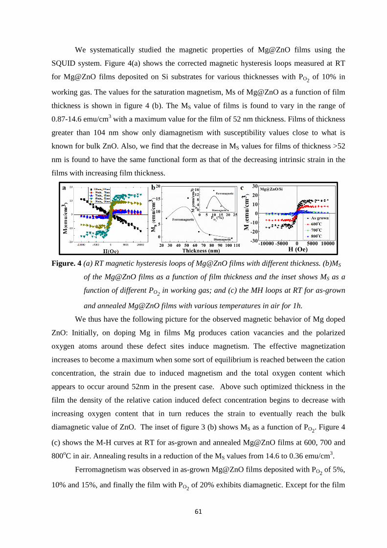
61
We systematically studied the magnetic properties of Mg@ZnO films using the
SQUID system. Figure 4(a) shows the corrected magnetic hysteresis loops measured at RT
for Mg@ZnO films deposited on Si substrates for various thicknesses with PO2 of 10% in
working gas. The values for the saturation magnetism, Ms of Mg@ZnO as a function of film
thickness is shown in figure 4 (b). The MS value of films is found to vary in the range of
0.87-14.6 emu/cm3 with a maximum value for the film of 52 nm thickness. Films of thickness
greater than 104 nm show only diamagnetism with susceptibility values close to what is
known for bulk ZnO. Also, we find that the decrease in MS values for films of thickness >52
nm is found to have the same functional form as that of the decreasing intrinsic strain in the
films with increasing film thickness.
Figure. 4 (a) RT magnetic hysteresis loops of Mg@ZnO films with different thickness. (b)MS
of the Mg@ZnO films as a function of film thickness and the inset shows MS as a
function of different PO2 in working gas; and (c) the MH loops at RT for as-grown
and annealed Mg@ZnO films with various temperatures in air for 1h.
We thus have the following picture for the observed magnetic behavior of Mg doped
ZnO: Initially, on doping Mg in films Mg produces cation vacancies and the polarized
oxygen atoms around these defect sites induce magnetism. The effective magnetization
increases to become a maximum when some sort of equilibrium is reached between the cation
concentration, the strain due to induced magnetism and the total oxygen content which
appears to occur around 52nm in the present case. Above such optimized thickness in the
film the density of the relative cation induced defect concentration begins to decrease with
increasing oxygen content that in turn reduces the strain to eventually reach the bulk
diamagnetic value of ZnO. The inset of figure 3 (b) shows MS as a function of PO2. Figure 4
(c) shows the M-H curves at RT for as-grown and annealed Mg@ZnO films at 600, 700 and
800oC in air. Annealing results in a reduction of the MS values from 14.6 to 0.36 emu/cm3.
Ferromagnetism was observed in as-grown Mg@ZnO films deposited with PO2 of 5%,
10% and 15%, and finally the film with PO2 of 20% exhibits diamagnetic. Except for the film

62
deposited with PO2 of 5%, both of MS and strain in the films decreases with increasing PO2
indicating that the magnetic moment in the films is related to the strain. The initial increase of
MS may be due to the increasing number of cation vacancies resulting from the collision
between oxygen atoms and Zn atoms during sputtering deposition in chamber, which reduces
the probability of the Zn atoms deposited on the substrate surface. However, at higher PO2
(more than 10%), the concentration of oxygen antisites and interstitials increase with the
increase of PO2, which promote the extinguishing of the active defects (cation vacancies)
resulting in a reduction of the net magnetization in the films followed by a diamagnetism of
the film deposited in PO2 of 20%. Also, the smaller Ms in the films with a thickness of ~26
nm in PO2 10% is maybe due to the weak texture that observed in XRD [18] as well as the
film deposited in PO2 10%. This may be related to the concentrations and types of defects in
the films.
The effects of annealing in air on the magnetization of Mg@ZnO films also
investigated. Figure 8 shows the magnetic hysteresis curves at RT for as-grown and annealed
Mg@ZnO films at 600, 700 and 800oC in air. Annealing resulted in a reduction in the MS
from 14.6 to 0.36 emu/cm3. When heated the Mg@ZnO films, re-evaporation of oxygen
occurred and this facilitated the formation of cation interstitial defects [19]. Thus ionic
compounds resulting from cation vacancies and cation interstitials reduce the concentration
of cation vacancies and thus MS decreases with the increase of annealing temperature
7.3.2 Fabrication of MgZnO films from Mg and Zn targets in (Ar+O2) Atmosphere
PROTOCOL.4:
Mg-doped ZnO films were deposited on Si and glass substrates by co-sputtering pure
Mg (99.99%) and Zn (99.99%) targets. The details are mentioned in protocol 3. The film
depositions were carried out at a fixed PO2 of 1.5 × 10⁻⁴ mbar in a mixture of Ar and O2 with
total pressure of 1.5 × 10⁻³ mbar, for different deposition times. Thermal treatment was
performed for the sample deposited at 90 min with the PO2 of 10% in working gas at 6000,
7000 and 8000C in air for 1h and the films prepared at 120 min were annealed at 5000C for 60
and 120 min.
Result and Discussions 3.2:
The deposition rate of the films was estimated to be 1.33 nm/min and the thickness of
the films was found to be in the range of 40-240 nm. From the EDS analysis, the atomic
concentration of Mg was found to be 6% (written as Mg0.06Zn0.94O). The SEM images of as-
grown Mg-doped ZnO films with thickness of 120 nm and 240 nm on Si substrates are shown

63
in figure 1(A&B). As thickness increases, the size and structure of the grains in the films
becomes more consistent.
Figure 1. SEM images of Mg-doped ZnO thin films prepared with thickness of (A)120 nm and
(B)240 nm, respectively; and (C) is the XRD patterns of the films with different
thickness on Si substrate.
Figure 2(C) shows the XRD patterns of Mg-doped ZnO thin films on Si substrates
with different thickness. The diffraction peaks corresponding to (100), (002) and (103) were
observed around at 30.64o, 33.98o and 62.37o, respectively. The peaks of (100) and (103)
appear in the film with thickness of 120 nm and become stronger in the films with thickness
more than 120 nm perhaps due to the changing defect and strain effects. The slight change in
the broadening of the peaks indicates the variation of the grain size. The average crystallite
size for the samples was estimated to be 8.9, 7.7, 6.9, 7.6, 8.5 and 8.3 nm for the films with
approximate thickness of 40, 80, 120, 160, 200 and 240 nm according to the analyses based
on the (002) peaks.
Figure 2 shows (αhv)2 plot of Mg0.06Zn0.94O thin films deposited on glass substrate as
a function of photon energy hv. Inset of the figure 2 shows that Band gap (Eg) as a function of
film thickness. As the films thickness increases the Eg decreases first from 3.48 to 3.42 eV
and then increases up to 3.52 eV.
Figure 2. Optical absorption spectra of Mg0.06Zn0.94O thin films deposited on glass substrates
and the inset shows corresponding optical Eg as a function of thickness.

64
There have been many measurements that show that the band gap of pure ZnO
depends on the method of preparation which affects both the oxygen stoichiometry and also
the grain size. The commonly quoted values for the band gap of pure ZnO are ~3.3 [20];
however it has recently been shown that gap can vary between 3.13eV and 4.06eV for films
deposited by MOCVD as the temperature of the substrate is varied [21]. The band width of
the mixed film MgZnO is expected to increase smoothly as x increases so long as it remains
in the wurzite structure. A recent theoretical work predicted that Eg(x) = Eg(0) +2.03x [22],
which compared well with some experimental results [23], and in this present work the value
of band gap is almost in agreement with the reported results ranging from 3.42 to 3.52 eV.
Our samples were deposited on Corning® Glass which starts to absorb at around 4 eV and
hence the measurements of the band edge were reliable only for energies below that value.
Mg doping increases the value of band gap compared to that of pure ZnO (3.37 eV).
The band gap value slightly varies with the thickness of the films due to the ambient growth
conditions related to defect, and strain among other parameters. Thus, it is clear that the Eg of
the Mg-doped ZnO films can be tuned by changing thickness of the films and growth
atmosphere. Also, we find the experimental results from the optical band gap are consistent
with the translation of phase to a crystalline character as suggested by the observed XRD
patterns. This may be attributed to that the concentration of defects (such as zinc vacancy,
and magnesium vacancy etc.) reaches maximum peak followed by reduction due to the
combination of changing nature and densities of the various defects when the thickness is
larger than 120 nm.
Figure. 3 (A) the saturation magnetization (MS) as a function of magnetic field (H) of the
as-grown Mg-doped ZnO films deposited on Si substrate with different thickness
and (B) MS as a function of film thickness.
Figure 3(A) shows the corrected magnetic hysteresis loops measured at room
temperature for the films deposited on Si substrates for various thicknesses. Ferromagnetism
was observed in all the as-grown Mg-doped ZnO films. The MS values as a function of film

65
thickness is shown in figure 3(B) and it varies in the ranges of ~1.3-15.76 emu/cm3 with a
maximum value for the film with 120 nm thickness.
The magnetism of the films may be due to the intrinsic complexities of cation and
other defects. Initially, doping Mg in films produces cation vacancies and the polarized
oxygen atoms around these defect sites induce ferromagnetism. The effective magnetization
increases to become a maximum when some sort of equilibrium is reached between the cation
vacancy concentration and the strain. Above such optimized thickness in the film, the density
of the relative cation induced defect concentration begins to decrease with combined effect of
other defects (such as zinc interstitial) to decrease magnetism.
Annealing Effect
Figure 4. XRD patterns of as-grown and annealed MgZnO films; (a) deposited at 90min with
different temperatures for1h and (b) the films deposited at 120 min for various
annealing times at 5000C.
The X-ray diffraction peaks of (100), (002) and (103) of the samples are marginally
shifted to higher angles after annealing, indicating that the strain is released after annealing at
high temperatures (see Figure 4). The intensity of the peaks in XRD patterns of annealed
samples sharply increases, indicating the films became more crystalline by annealing. The
improvement of the film crystallinity may be due to the increasing of the mobility of the
atoms during annealing.
Figure 5(a) shows the magnetic hysteresis curves at RT for as-grown film with a
thickness of ~ 120 nm and annealed at 600, 700 and 800OC in air for 1h and figure 5(b)
shows the M-H of as-grown and annealed films with a thickness of ~160 nm various
annealing times at 500OC. Annealing resulted in a considerable reduction in the MS values
from ~15.6 to1.069 emu/cm3 and ~8.6 to 0.9emu/cm3 for the films with thickness ~120 and
160 nm, respectively. Re-evaporation of oxygen occurred and this facilitated the formation of
cation interstitial defects during annealing [24]. Thus ionic compounds resulting from cation

66
vacancies and cation interstitials reduce the concentration of cation vacancies and MS
decreases with the increase of annealing temperature.
Figure. 5 The saturation magnetization (MS) as a function of magnetic field (H) of the as-
grown and annealed Mg-doped ZnO films (a) the MH loops at RT for as-grown
and annealed Mg@ZnO films with various temperatures in air for 1h.
VII. 4 Electronic Structure of Room temperature ferromagnetic MgO and MgZnO Thin
Films (Supplement VI)
To understand the charge state, local environment, electronic structure, information
on the orientation of adsorbed molecules, hybridization etc of specific cations present in the
MgO/MgZnO material, we performed NEXAFS experiment. The sample details are given
below.
Table 1. Sample details
Sample code
Composition Sputtering Ambience
Power Thickness (~nm)
Total Pressure (mBar)
S1 MgO Ar+O2 Mg-C~40W 38 1.5×10⁻³ S2 MgO N2+O2 Mg-DC-60W 38 3.0×10⁻³ S3 MgO N2+O2 Mg-C~55W 115 1.5×10⁻³ S4 Mg0.16Zn0.84OY N2+O2 Mg-C~10W
Zn-RF-50W 51 1.5×10⁻³
Figure 1 shows the NEXAFS spectrum of the thin films. Mg K-edge NEXAFS spectra
of the series of the thin films have been presented in Figure 1(a), reflecting the Mg 1s→3pd
and 4s state transitions and hybridization of the same with O 2p. Energy calibration has been
performed using the Mg K-edge peak of MgO at 1311.3 eV. Figure 1(b) is the O K-edge
NEXAFS spectra (total density un-occupied of states) of the thin films arising from the
excitation of oxygen 1s core electrons (excitation energy 510-580 eV) into its unoccupied 2p
states, and the hybridization of the same with Mg 3spd states. Figure 1 (c) depicting the N K-

67
edge NEXAFS spectra representing the N 1s →3sp transitions. Feature I in the intrinsic MgO
is as of now unidentified.
Figure 1. NEXAFS spectra: (a) Mg K-edge; (b) O K-edge (total density un-occupied of
states); and (c) N K-edge NEXAFS spectra of the thin films
The peak E has previously also been observed in the series of Fe doped MgO thin
films deposited by Ink Jet printing where the origin of the feature was attributed to the
unoccupied O 2p states [25].This unoccupied sate is originated due to cation vacancy (VMg).
If there wouldn't exist any cation vacancies then there should have been a strong
hybridization between the cation ion and the oxygen 2p, and the peak E shouldn't exist. Such
unoccupied states are only present in the case when N2 has been introduced into the
MgO/MgZnO system.
7. 5 Suppression of Ferromagnetic Ordering in thick co-sputtered Mn doped MgO
Films (Supplement-VII)
Fabrication of MnMgO films
PROTOCOL.5:
Mn doped MgO thin films were prepared on Si substrates by co-sputtering pure Mn
(99.99%) and Mg (99.99%) targets at room temperature. The sputtering chamber was
evacuated to 10-6 mbar. Prior to film growth, the targets were pre-cleaned by sputtering for 30
minutes in the presence of Ar. We prepared two series of samples of different thickness
containing low (14 at.%) and high (53 at.%) Mn concentrations respectively under the
following conditions: The series of the films containing 14 at.% Mn were deposited with
direct current (DC) power of ~ 43W used on Mg target and the radio frequency (RF) power
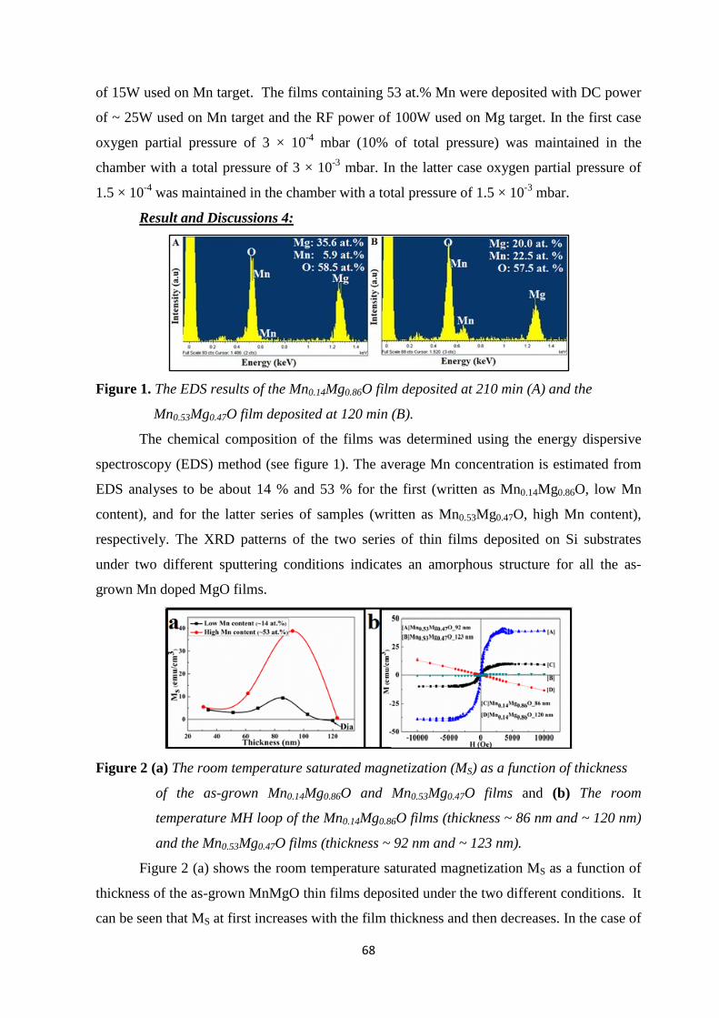
68
of 15W used on Mn target. The films containing 53 at.% Mn were deposited with DC power
of ~ 25W used on Mn target and the RF power of 100W used on Mg target. In the first case
oxygen partial pressure of 3 × 10⁻⁴ mbar (10% of total pressure) was maintained in the
chamber with a total pressure of 3 × 10⁻³ mbar. In the latter case oxygen partial pressure of
1.5 × 10⁻⁴ was maintained in the chamber with a total pressure of 1.5 × 10⁻³ mbar.
Result and Discussions 4:
Figure 1. The EDS results of the Mn0.14Mg0.86O film deposited at 210 min (A) and the
Mn0.53Mg0.47O film deposited at 120 min (B).
The chemical composition of the films was determined using the energy dispersive
spectroscopy (EDS) method (see figure 1). The average Mn concentration is estimated from
EDS analyses to be about 14 % and 53 % for the first (written as Mn0.14Mg0.86O, low Mn
content), and for the latter series of samples (written as Mn0.53Mg0.47O, high Mn content),
respectively. The XRD patterns of the two series of thin films deposited on Si substrates
under two different sputtering conditions indicates an amorphous structure for all the as-
grown Mn doped MgO films.
Figure 2 (a) The room temperature saturated magnetization (MS) as a function of thickness
of the as-grown Mn0.14Mg0.86O and Mn0.53Mg0.47O films and (b) The room
temperature MH loop of the Mn0.14Mg0.86O films (thickness ~ 86 nm and ~ 120 nm)
and the Mn0.53Mg0.47O films (thickness ~ 92 nm and ~ 123 nm).
Figure 2 (a) shows the room temperature saturated magnetization MS as a function of
thickness of the as-grown MnMgO thin films deposited under the two different conditions. It
can be seen that MS at first increases with the film thickness and then decreases. In the case of
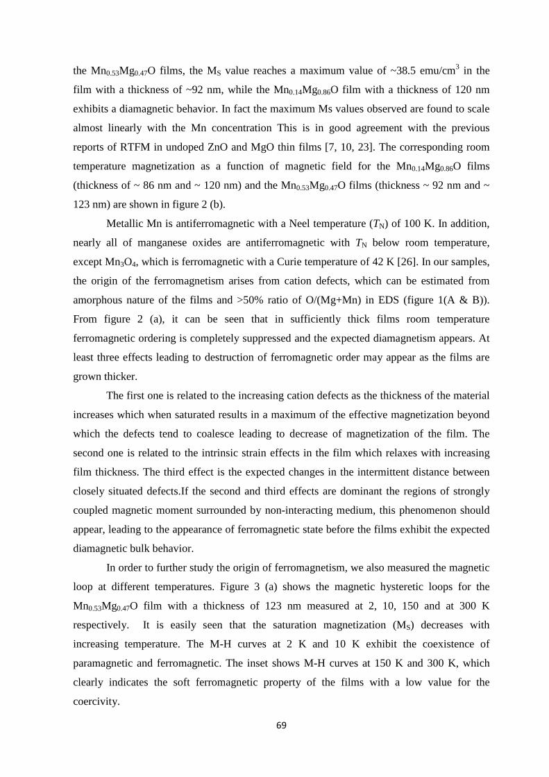
69
the Mn0.53Mg0.47O films, the MS value reaches a maximum value of ~38.5 emu/cm3 in the
film with a thickness of ~92 nm, while the Mn0.14Mg0.86O film with a thickness of 120 nm
exhibits a diamagnetic behavior. In fact the maximum Ms values observed are found to scale
almost linearly with the Mn concentration This is in good agreement with the previous
reports of RTFM in undoped ZnO and MgO thin films [7, 10, 23]. The corresponding room
temperature magnetization as a function of magnetic field for the Mn0.14Mg0.86O films
(thickness of ~ 86 nm and ~ 120 nm) and the Mn0.53Mg0.47O films (thickness ~ 92 nm and ~
123 nm) are shown in figure 2 (b).
Metallic Mn is antiferromagnetic with a Neel temperature (TN) of 100 K. In addition,
nearly all of manganese oxides are antiferromagnetic with TN below room temperature,
except Mn3O4, which is ferromagnetic with a Curie temperature of 42 K [26]. In our samples,
the origin of the ferromagnetism arises from cation defects, which can be estimated from
amorphous nature of the films and >50% ratio of O/(Mg+Mn) in EDS (figure 1(A & B)).
From figure 2 (a), it can be seen that in sufficiently thick films room temperature
ferromagnetic ordering is completely suppressed and the expected diamagnetism appears. At
least three effects leading to destruction of ferromagnetic order may appear as the films are
grown thicker.
The first one is related to the increasing cation defects as the thickness of the material
increases which when saturated results in a maximum of the effective magnetization beyond
which the defects tend to coalesce leading to decrease of magnetization of the film. The
second one is related to the intrinsic strain effects in the film which relaxes with increasing
film thickness. The third effect is the expected changes in the intermittent distance between
closely situated defects.If the second and third effects are dominant the regions of strongly
coupled magnetic moment surrounded by non-interacting medium, this phenomenon should
appear, leading to the appearance of ferromagnetic state before the films exhibit the expected
diamagnetic bulk behavior.
In order to further study the origin of ferromagnetism, we also measured the magnetic
loop at different temperatures. Figure 3 (a) shows the magnetic hysteretic loops for the
Mn0.53Mg0.47O film with a thickness of 123 nm measured at 2, 10, 150 and at 300 K
respectively. It is easily seen that the saturation magnetization (MS) decreases with
increasing temperature. The M-H curves at 2 K and 10 K exhibit the coexistence of
paramagnetic and ferromagnetic. The inset shows M-H curves at 150 K and 300 K, which
clearly indicates the soft ferromagnetic property of the films with a low value for the
coercivity.

70
Figure 3. (a) The magnetization (M) of the Mn0.53Mg0.47O film with a thickness of 123 nm as
a function of magnetic field (H) at 2, 10, 150 & 300 K, respectively (the inset
shows the enlarged M-H at 150, and 300 K) and (b) Temperature dependence of
ZFC magnetic moment (M) recorded in a field of 2 kOe, and the remnant magnetic
moment Mrem, recorded after cooling the sample in 2 kOe and switching off the
magnetic field forMn0.53Mg0.47O film with a thickness of 123 nm. The inset shows
the temperature dependence of the difference (∆M), MZFC–Mrem, curve.
Figure 3(b) shows the temperature dependence of the zero-field cooled magnetic
moment (MZFC) recorded in a magnetic field of 2 kOe and of remnant magnetic moment
(Mrem) recorded after cooling the sample in 2 kOe and then switching off the magnetic field
for the high Mn content MgO film with a thickness of 123 nm. The temperature dependence
of the difference in magnetic moment [ΔM=MZFC(T)-Mrem(T)], is shown in the inset of the
figure 3(b). Ferromagnetism is generally attributed to the observed hysteresis. Also spin
glass effects, co-operative interactions between superparamagnetic clusters, or blocked super
paramagnetic clusters would produce similar behavior. Whereas, spin glass temperatures and
blocking temperatures for superparamagnetic clusters tend to be at temperatures less than
∼100 K.

71
7. 6 References
[1] A. Biswas, W. Shirong, S. Nagar, L. Belova, K. V. Rao, MRS Symp. Proc., 1292, 117(2011) [2] F. H. Arag´on, J. A. H. Coaquira, P. Hidalgo, S. L. M. Brito, D. Gouvêa, R. H. R. Castro. J. Phys.: Condens. Matter 22 (2010) 496003 [3] F. G. Wang, Z. Y. Pang, L. Lin, S. J. Fang, Y. Dai, S. H. Han. Phys.Rev.B80 (2009)144424. [4] H. K.Yu, J.-L. Lee. Cryst. Growth. Des.10 (2010) 5200. [5] C. Martínez Boubeta, A. Cebollada, J. F. Calleja, C. Contreras, F. Peirό, and A. Cornet. J. Appl.Phys.93(2003)2126. [6] D. Cáceres, I. Vergara, R. González. J.Appl.Phys.93(2003)4300. [7] C. Moyses Araujo, M. Kapilashrami, Xu Jun, O. D. Jayakumar, S. Nagar, Y.Wu, C. Århammar, B. Johansson,L. Belova, R. Ahuja, G. A. Gehring, K. V. Rao, Appl.Phys.Lett.96 (2010)232505. [8] M. Kapilashrami, J. Xu, V. Ström, K. V. Rao, L. Belova. Appl. Phys. Lett.95 (2009) 033104. [9] D. Y. Kim, J. S Hong, Y. R. Park, K. J. Kim. J. Phys.: Condens. Matter 21 (2009) 195405. [10] N. H. Hong, J. Sakai, N. Poirot, V. Brizé. Phys.Rev.B73(2006)132404. [11] F. Gao, J. F. Hu, C. L. Yang, Y. J. Zheng, H. W. Qin, L. Sun, X. W. Kong, M. H. Jiang. Solid State Commun.149(2009)855. [12] M. Kapilashrami, J. Xu, K. V. Rao, L. Belova, E. Carlegrim, M. Fahlman, J. Phys.: Condens. Matter 22(2010)345004. [13] E.M. Bachari, G. Baud, S. Ben Amor, M. Jacquet, Thin Solid Films 165, 348, (1999). [14] K. H. L. Zhang, V. K. Lazarov, T. D. Veal, F. E. Oropeza, C. F. McConville, R. G. Egdell and A. Walsh J. Phys.: Condens. Matter 23 (2011) 334211. [15] T. S. Moss, Proc. Phys. Soc. London, Sect. B 67, 775 (1954). [16] S. Suwanboon, P. Amornpitoksuk, A. Sukolrat, Ceram. Int. 37 (2011) 1359. [17] K. Huanga, Z. Tanga, L. Zhanga, J. Yua, J. Lvb, X. Liuc, F. Liud, Applied Surface Science 258 (2012) 3710– 3713; S. Suwanboon, P. Amornpitoksuk, A. Sukolrat, Ceram. Int. 37 (2011) 1359. [18] B. Straumal, A. Mazilkin, S. Protasova, A. Myatiev, P. Straumal, E. Goering, B. Baretzky, Phys. Status Solidi B 248, No. 7, 1581–1586 (2011) [19] J. Li, J-H Huang, W-J Song, Y-L Zhang, R-Q Tan, Y. Yang. J. Crystal growth 314, 136 (2011). [20] Ü. Özgür, Ya. I. Alivov, C. Liu, A. Teke, M. A. Reshchikov, S. Doğan, V. Avrutin, S.- J.Cho, and H. Morkoçd, J. Appl. Phys. 98, 041301(2005). [21] S. T. Tan, B. J. Chen, X. W. Sun, W. J. Fan, H. S. Kwok, X. H. Zhang, and S. J. Chua, J. Appl. Phys. 98, 013505(2005). [22] C. Franz, M. Giar, M. Heinemann, M. Czerner, and C. Heiliger, MRS Proceedings, 1494, mrsf12-1494-z04-32 doi:10.1557/opl.2012.1709 (2013). [23] A. Ohtomo, M. Kawasaki, T. Koida, K. Masubuchi, H. Koinuma, Y. Sakurai, Y. Yoshida, T. Yasuda, and Y. Segawa, Appl. Phys. Lett. 72, 2466 (1998). [24] J. Li, J-H Huang, W-J Song, Y-L Zhang, R-Q Tan, Y. Yang. J. Crystal growth 314, 136 (2011). [25] M. Kapilashrami, H. Zhang,M. Fang, X. Li, X. Sun, K. V. Rao, L. Belova, Y. Luo, and J Guo, Appl. Phys. Lett. 101 082411 (2012) [26] C. N. R. Rao and B. Raveau, Transition Metal Oxides, 2nd edn, Wiley-VCH, Germany (1995).

72
73
Chapter 8
Summary and overview of supplements
8.1 Room temperature ferromagnetism of Metal oxide thin films
8.1.1 Comparative study of room temperature ferromagnetism in MgO films deposited by
sputtering Mg and MgO targets
MgO films were prepared on glass and Si substrates by sputtering Mg and MgO
targets, which show RTFM. The films deposited from Mg target were mostly amorphous
while the films from MgO targets were more nanocrystalline in structure. The maximum MS
values of MgO films prepared from Mg and MgO targets are ~13.75emu/g and ~4.2 emu/g,
respectively, indicating that the defect structure and there densities are different in the two
cases. The saturation magnetization (MS) of MgO films increases at first as the film’s
thickness increases and then decreases, with a maximum value clearly depending on the
nature of the target used. The observed MS values are much higher in the case of films
deposited from metallic target when compared to those obtained from a composite MgO
target.
8.1.2 Magnetism of amorphous and nanocrystalized dc-sputter-deposited MgO Thin Films
MgO films were grown on Si substrates by sputtering from a metallic Mg target with
various O2 contents in working gas, and the effects of thermal annealing on the structural and
magnetic properties were investigated. Our results reveal that there exists a close correlation
between the room temperature ferromagnetism, the crystallinity, and the magnesium vacancy
concentrations in the MgO thin films. All as-grown films were amorphous due to the large
lattice mismatch between MgO and Si substrate. After annealing, the films became crystalline
and the MS values decreases. The origin of the RTFM could be attributed to the Mg
vacancies. The PO2 in working gas play an important role to determine the MS value of as-
grown MgO films. When PO2 increased from 10% to 80%, MS values initially increased up to
PO2 of 40% and then decreases at higher oxygen content in the working gas. EDS results
show that the ratio of O/Mg in MgO films is greater than 1, indicating the presence of high

74
density of Mg vacancies in MgO films. Furthermore, we have found that less crystallinity can
increase the ferromagnetism of MgO thin films due to larger amounts of Mg vacancies. Our
results not only demonstrate an important approach to obtain room temperature ferromagnetic
MgO films but also help to understand the origin of ferromagnetism in MgO films.
8.2 Room Temperature Ferromagnetism and Band Gap Investigations in Mg Doped
ZnO RF/DC Sputtered Films
8.2.1 Fabrication of MgZnO films from Mg and Zn targets in (N2+O2) Atmosphere
Mg@ZnO films were prepared on Si and glass substrates by co-sputtering Mg and Zn
targets in (N2+O2) ambience. We observed the Eg of the films varies with O2 partial pressure
in the working gas, which may be ascribed to the variation of Mg content in the films. The
RTFM was observed in Mg@ZnO films prepared on Si. With the increase in film thickness
and PO2, a transition from ferromagnetic to diamagnetic behavior was observed which is
attributed to the cation defect induced strain. The intrinsic strain and the texture in the films
play an important role in structural and magnetic properties in Mg@ZnO films.
8.2.2 Fabrication of MgZnO films from Mg and Zn targets in (Ar+O2) Atmosphere
Mg doped ZnO films were prepared on Si substrates by co-sputtering Mg and Zn
targets. We observed the Eg of the films varies with thickness, which may be ascribed to the
growth condition and Mg doping. The RTFM was observed in all the Mg-doped ZnO films
prepared on Si. With the increase in film thickness, a transition from ferromagnetic to
diamagnetic behavior was observed which is attributed to the cation defect induced strain.
The intrinsic defects in the films play an important role in structural and magnetic properties
in Mg-doped ZnO films.
8.3 Electronic Structure of Room temperature ferromagnetic MgO and MgZnO Thin
Films
MgO/MgZnO films have been deposited by Mg, Zn targets. We performed Mg K-
edge NEXAFS experiment in order to understand the charge state, local environment,
electronic structure, information on the orientation of adsorbed molecules, hybridization etc
of specific cations present in the thin films. Experimental studies reveals that the presence of
unoccupied O 2p states. This unoccupied sate is originated due to cation vacancy (VMg). Such

75
unoccupied states are only present in the case when N has been introduced into the
MgO/MgZnO system. So we conclude that the observed ferromagnetism in MgO/MgZnO
system is originating from the coupling between 2p states of the oxygen atoms surrounding a
cation vacancy site.
VIII.4 Suppression of Ferromagnetic Ordering in Thick Co-sputtered Mn doped MgO
Films
Mn doped MgO films have been deposited by co-sputtering from Mn and Mg targets.
The structural, surface morphologies and magnetic properties of the films were studied. All
the as grown films are amorphous and film surfaces are homogeneous. The magnetic phase
transition as a function of film thickness is observed in our experiments and room
temperature saturation magnetism value reaches a maximum value of ~38.5 emu/cm3 in the
Mn0.53Mg0.47O with a thickness of ~92 nm. The suppression of ferromagnetism in thick films
can be explained in terms of the reduction of defects at cation site and reduction of strain at
higher film thickness. Also, the magnetization of the as grown samples had significant
reduces as they aged in ambient air condition.

76

77
Chapter 9
Suggestions for Future Work
In the future, the quantification studies on how the doping concentration of Mg
content affects the band gap and magnetization of the MgXZn1-XO thin films, and how the
strain affects the ferromagnetic properties of the films could be carried out. By preparing Mg
doped ZnO thin films by co-sputtering with different targets, i.e., Mg, Zn metallic, MgO and
ZnO ceramic target on different substrates (Si, Sapphire, quartz, glass etc.), the studies on
what changes on the crystal structure of the MgXZn1-XO thin films could result with different
targets and substrates, and further how to tune the band structure and magnetization of the
films could be studied. Also we could prepare MnXMg1-X O films by co-sputtering of
different targets i.e., Mn, Mg, MnO and MgO. The future plan covers the study how the
magnetization of the films would change with different RF/DC power supply. The in- depth
studies on magnetic properties of the films can be carried out by NEXAS and XMCD.

78