Mälardalen University
73
Mälardalen University MÝãÙ ã«Ý®Ý CEL505 GOVERNOR ELECTRONICS FOR DIESEL ENGINES High availability plaƞorm for real-Ɵme control and advanced fuel efficiency algorithms Author: Johnny Holmström [email protected] University Supervisors: Prof. Lars Asplund [email protected] Ass. Prof. Mikael Ekström [email protected] Company supervisors: M.Sc Tomas Lindqvist [email protected] Prof. George Fodor [email protected] Arne Löfgren [email protected] July 15, 2013 Västerås, Sweden
Transcript of Mälardalen University

Mälardalen University
M CEL505
GOVERNOR ELECTRONICS FOR DIESEL ENGINES
High availability pla orm for real- me control and advancedfuel efficiency algorithms
Author:Johnny Holmströ[email protected]
University Supervisors:Prof. Lars [email protected]. Prof. Mikael Ekströ[email protected]
Company supervisors:M.Sc Tomas [email protected]
Prof. George [email protected]
Arne Lö[email protected]
July 15, 2013Västerås, Sweden
Mälardalen University DEGO IV
Abstract
Fossil fuel is a rare commodity and the combus on of this fuel results in nega ve environmental effects. Thispaper evaluates and validates the electronics needed to run intelligent algorithms to lower the fuel consump-on for commercial vessels. This is done by integra ng advanced fuel saving func ons into an electronic device
that controls the fuel injec on of large diesel engines, as known as a diesel engine governor.
The control system is classified as a safety cri cal system. This means that the electronics needs to be de-signed for fail safe opera on. To allow for future research and development, the pla orm needs flexibilityin respect to hardware reconfigura on and so ware changes, i.e. this is the basis for a system that allowsfor hardware-so ware co-design. For efficient installa on and easy commissioning, the system shall allow forauto-calibra on combined with programmable jumper selec ons to a ain a cost effec ve solu on.
The computa on of the fuel saving algorithm require accurate data to build a model of the vessels mo ons.This is achieved by integra ng state of the art sensors and a mul tude of communica on interfaces. Amongother things gyroscopes contra accelerometers where evaluated to find the best solu on in respect to cost andperformance.
This design replace the current product DEGO III. The new product requires the same func onality and shallallow for more func ons. Focus has been spent on communica on, methods of accruing sensor data and morecomputa on speed. In crea ng a new genera on of a product there are tasks like selec ng components, ques-ons pertaining to layout of the printed circuit board and an evalua on of supply chains. The manufacturing
aspects are considered to ra onalize produc on and tes ng.
1
Mälardalen University DEGO IV
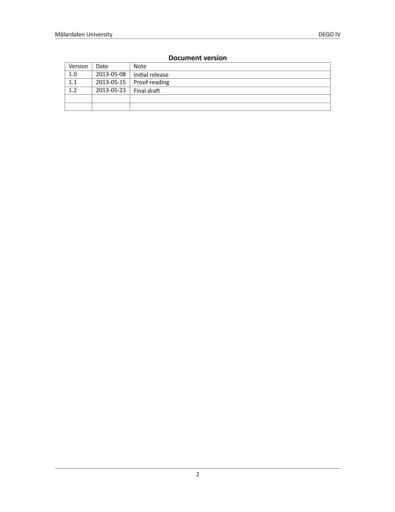
Document versionVersion Date Note1.0 2013-05-08 Ini al release1.1 2013-05-15 Proof-reading1.2 2013-05-23 Final dra
2
Mälardalen University DEGO IV
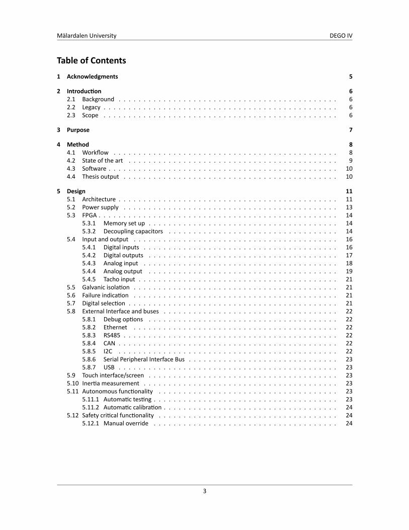
Table of Contents1 Acknowledgments 5
2 Introduc on 62.1 Background . . . . . . . . . . . . . . . . . . . . . . . . . . . . . . . . . . . . . . . . . . . . 62.2 Legacy . . . . . . . . . . . . . . . . . . . . . . . . . . . . . . . . . . . . . . . . . . . . . . . 62.3 Scope . . . . . . . . . . . . . . . . . . . . . . . . . . . . . . . . . . . . . . . . . . . . . . . 6
3 Purpose 7
4 Method 84.1 Workflow . . . . . . . . . . . . . . . . . . . . . . . . . . . . . . . . . . . . . . . . . . . . . 84.2 State of the art . . . . . . . . . . . . . . . . . . . . . . . . . . . . . . . . . . . . . . . . . . 94.3 So ware . . . . . . . . . . . . . . . . . . . . . . . . . . . . . . . . . . . . . . . . . . . . . . 104.4 Thesis output . . . . . . . . . . . . . . . . . . . . . . . . . . . . . . . . . . . . . . . . . . . 10
5 Design 115.1 Architecture . . . . . . . . . . . . . . . . . . . . . . . . . . . . . . . . . . . . . . . . . . . . 115.2 Power supply . . . . . . . . . . . . . . . . . . . . . . . . . . . . . . . . . . . . . . . . . . . 135.3 FPGA . . . . . . . . . . . . . . . . . . . . . . . . . . . . . . . . . . . . . . . . . . . . . . . . 14
5.3.1 Memory set up . . . . . . . . . . . . . . . . . . . . . . . . . . . . . . . . . . . . . . 145.3.2 Decoupling capacitors . . . . . . . . . . . . . . . . . . . . . . . . . . . . . . . . . . 14
5.4 Input and output . . . . . . . . . . . . . . . . . . . . . . . . . . . . . . . . . . . . . . . . . 165.4.1 Digital inputs . . . . . . . . . . . . . . . . . . . . . . . . . . . . . . . . . . . . . . . 165.4.2 Digital outputs . . . . . . . . . . . . . . . . . . . . . . . . . . . . . . . . . . . . . . 175.4.3 Analog input . . . . . . . . . . . . . . . . . . . . . . . . . . . . . . . . . . . . . . . 185.4.4 Analog output . . . . . . . . . . . . . . . . . . . . . . . . . . . . . . . . . . . . . . 195.4.5 Tacho input . . . . . . . . . . . . . . . . . . . . . . . . . . . . . . . . . . . . . . . . 21
5.5 Galvanic isola on . . . . . . . . . . . . . . . . . . . . . . . . . . . . . . . . . . . . . . . . . 215.6 Failure indica on . . . . . . . . . . . . . . . . . . . . . . . . . . . . . . . . . . . . . . . . . 215.7 Digital selec on . . . . . . . . . . . . . . . . . . . . . . . . . . . . . . . . . . . . . . . . . . 215.8 External Interface and buses . . . . . . . . . . . . . . . . . . . . . . . . . . . . . . . . . . . 22
5.8.1 Debug op ons . . . . . . . . . . . . . . . . . . . . . . . . . . . . . . . . . . . . . . 225.8.2 Ethernet . . . . . . . . . . . . . . . . . . . . . . . . . . . . . . . . . . . . . . . . . 225.8.3 RS485 . . . . . . . . . . . . . . . . . . . . . . . . . . . . . . . . . . . . . . . . . . . 225.8.4 CAN . . . . . . . . . . . . . . . . . . . . . . . . . . . . . . . . . . . . . . . . . . . . 225.8.5 I2C . . . . . . . . . . . . . . . . . . . . . . . . . . . . . . . . . . . . . . . . . . . . 225.8.6 Serial Peripheral Interface Bus . . . . . . . . . . . . . . . . . . . . . . . . . . . . . . 235.8.7 USB . . . . . . . . . . . . . . . . . . . . . . . . . . . . . . . . . . . . . . . . . . . . 23
5.9 Touch interface/screen . . . . . . . . . . . . . . . . . . . . . . . . . . . . . . . . . . . . . . 235.10 Iner a measurement . . . . . . . . . . . . . . . . . . . . . . . . . . . . . . . . . . . . . . . 235.11 Autonomous func onality . . . . . . . . . . . . . . . . . . . . . . . . . . . . . . . . . . . . 23
5.11.1 Automa c tes ng . . . . . . . . . . . . . . . . . . . . . . . . . . . . . . . . . . . . . 235.11.2 Automa c calibra on . . . . . . . . . . . . . . . . . . . . . . . . . . . . . . . . . . . 24
5.12 Safety cri cal func onality . . . . . . . . . . . . . . . . . . . . . . . . . . . . . . . . . . . . 245.12.1 Manual override . . . . . . . . . . . . . . . . . . . . . . . . . . . . . . . . . . . . . 24
3
Mälardalen University DEGO IV
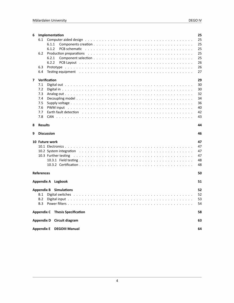
6 Implementa on 256.1 Computer aided design . . . . . . . . . . . . . . . . . . . . . . . . . . . . . . . . . . . . . . 25
6.1.1 Components crea on . . . . . . . . . . . . . . . . . . . . . . . . . . . . . . . . . . . 256.1.2 PCB schema c . . . . . . . . . . . . . . . . . . . . . . . . . . . . . . . . . . . . . . 25
6.2 Produc on prepara ons . . . . . . . . . . . . . . . . . . . . . . . . . . . . . . . . . . . . . 256.2.1 Component selec on . . . . . . . . . . . . . . . . . . . . . . . . . . . . . . . . . . . 256.2.2 PCB Layout . . . . . . . . . . . . . . . . . . . . . . . . . . . . . . . . . . . . . . . . 26
6.3 Prototype . . . . . . . . . . . . . . . . . . . . . . . . . . . . . . . . . . . . . . . . . . . . . 266.4 Tes ng equipment . . . . . . . . . . . . . . . . . . . . . . . . . . . . . . . . . . . . . . . . 27
7 Verifica on 297.1 Digital out . . . . . . . . . . . . . . . . . . . . . . . . . . . . . . . . . . . . . . . . . . . . . 307.2 Digital in . . . . . . . . . . . . . . . . . . . . . . . . . . . . . . . . . . . . . . . . . . . . . . 307.3 Analog out . . . . . . . . . . . . . . . . . . . . . . . . . . . . . . . . . . . . . . . . . . . . . 327.4 Decoupling model . . . . . . . . . . . . . . . . . . . . . . . . . . . . . . . . . . . . . . . . . 347.5 Supply voltage . . . . . . . . . . . . . . . . . . . . . . . . . . . . . . . . . . . . . . . . . . . 367.6 PWM input . . . . . . . . . . . . . . . . . . . . . . . . . . . . . . . . . . . . . . . . . . . . 407.7 Earth fault detec on . . . . . . . . . . . . . . . . . . . . . . . . . . . . . . . . . . . . . . . 427.8 CAN . . . . . . . . . . . . . . . . . . . . . . . . . . . . . . . . . . . . . . . . . . . . . . . . 43
8 Results 44
9 Discussion 46
10 Future work 4710.1 Electronics . . . . . . . . . . . . . . . . . . . . . . . . . . . . . . . . . . . . . . . . . . . . . 4710.2 System integra on . . . . . . . . . . . . . . . . . . . . . . . . . . . . . . . . . . . . . . . . 4710.3 Further tes ng . . . . . . . . . . . . . . . . . . . . . . . . . . . . . . . . . . . . . . . . . . 47
10.3.1 Field tes ng . . . . . . . . . . . . . . . . . . . . . . . . . . . . . . . . . . . . . . . . 4810.3.2 Cer fica on . . . . . . . . . . . . . . . . . . . . . . . . . . . . . . . . . . . . . . . . 48
References 50
Appendix A Logbook 51
Appendix B Simula ons 52B.1 Digital switches . . . . . . . . . . . . . . . . . . . . . . . . . . . . . . . . . . . . . . . . . . 52B.2 Digital input . . . . . . . . . . . . . . . . . . . . . . . . . . . . . . . . . . . . . . . . . . . . 53B.3 Power filters . . . . . . . . . . . . . . . . . . . . . . . . . . . . . . . . . . . . . . . . . . . . 54
Appendix C Thesis Specifica on 58
Appendix D Circuit diagram 63
Appendix E DEGOIII Manual 64
4

Mälardalen University DEGO IV
1 AcknowledgmentsDuring this master thesis there has been support and help. Apprecia on bestow Q-TAGG for support in re-sources and trust. Jörgen Bosson has been a great resource during the project examining solu ons and im-plementa ons. A special thanks is given to Lennart Lindh for his advisement. Per Lenander did a splendid jobon se ng a standard and explaining his work in the preliminary inves ga on. Large apprecia on is given toCograpro in Gothenburg, Sweden andWürth Elektronik in Germany for their advice on PCB manufacture. Elek-tronikMekanik in Västerås has given helpful comments on component selec on and assembly. Mar n Ekströmis recognized for many s mula ng discussions. A final men on goes to Bobo Lillqvist, Andreas Domfors andThomas Pe ersson for reading the first dra of the report.
5
Mälardalen University DEGO IV
2 Introduc on
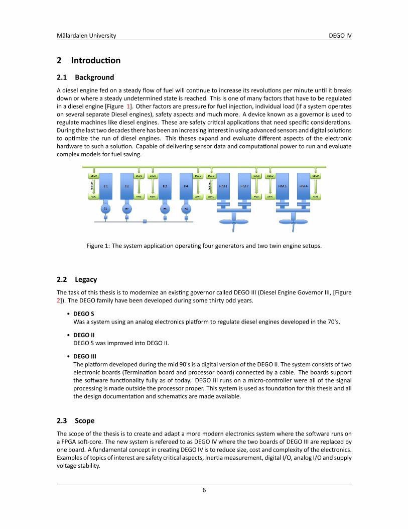
2.1 BackgroundA diesel engine fed on a steady flow of fuel will con nue to increase its revolu ons per minute un l it breaksdown or where a steady undetermined state is reached. This is one of many factors that have to be regulatedin a diesel engine [Figure 1]. Other factors are pressure for fuel injec on, individual load (if a system operateson several separate Diesel engines), safety aspects and much more. A device known as a governor is used toregulate machines like diesel engines. These are safety cri cal applica ons that need specific considera ons.During the last twodecades there has been an increasing interest in using advanced sensors anddigital solu onsto op mize the run of diesel engines. This theses expand and evaluate different aspects of the electronichardware to such a solu on. Capable of delivering sensor data and computa onal power to run and evaluatecomplex models for fuel saving.
Figure 1: The system applica on opera ng four generators and two twin engine setups.
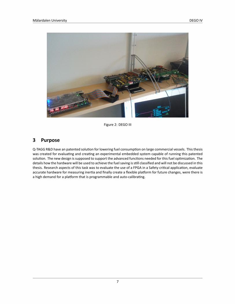
2.2 LegacyThe task of this thesis is to modernize an exis ng governor called DEGO III (Diesel Engine Governor III, [Figure2]). The DEGO family have been developed during some thirty odd years.
• DEGO SWas a system using an analog electronics pla orm to regulate diesel engines developed in the 70's.
• DEGO IIDEGO S was improved into DEGO II.
• DEGO IIIThe pla orm developed during the mid 90's is a digital version of the DEGO II. The system consists of twoelectronic boards (Termina on board and processor board) connected by a cable. The boards supportthe so ware func onality fully as of today. DEGO III runs on a micro-controller were all of the signalprocessing is made outside the processor proper. This system is used as founda on for this thesis and allthe design documenta on and schema cs are made available.
2.3 ScopeThe scope of the thesis is to create and adapt a more modern electronics system where the so ware runs ona FPGA so -core. The new system is refereed to as DEGO IV where the two boards of DEGO III are replaced byone board. A fundamental concept in crea ng DEGO IV is to reduce size, cost and complexity of the electronics.Examples of topics of interest are safety cri cal aspects, Iner ameasurement, digital I/O, analog I/O and supplyvoltage stability.
6
Mälardalen University DEGO IV
Figure 2: DEGO III
3 PurposeQ-TAGG R&D have an patented solu on for lowering fuel consump on on large commercial vessels. This thesiswas created for evalua ng and crea ng an experimental embedded system capable of running this patentedsolu on. The new design is supposed to support the advanced func ons needed for this fuel op miza on. Thedetails how the hardware will be used to achieve the fuel saving is s ll classified andwill not be discussed in thisthesis. Research aspects of this task was to evaluate the use of a FPGA in a Safety cri cal applica on, evaluateaccurate hardware for measuring iner a and finally create a flexible pla orm for future changes, were there isa high demand for a pla orm that is programmable and auto-calibra ng.
7
Mälardalen University DEGO IV
4 Method
4.1 WorkflowThe documenta on primarily consists of the thesis report. The report served as a development tool wereideas were developed and also shared among supervisors, during the final phase of the thesis the results weredocumented. The report were con nuously updated, showing the latest progress. This thesis is divided anddocumented in separate phases. First is the method describing how the thesis was performed. Following themethod is the design (Sec on 5) where different possible designs to solve the problem are discussed. This dis-cussion leads to the implementa on (Sec on 6) where the manufacturing of the PCB´s is documented. Finallythe results are presented followed by the conclusion of these results (Sec on 7).
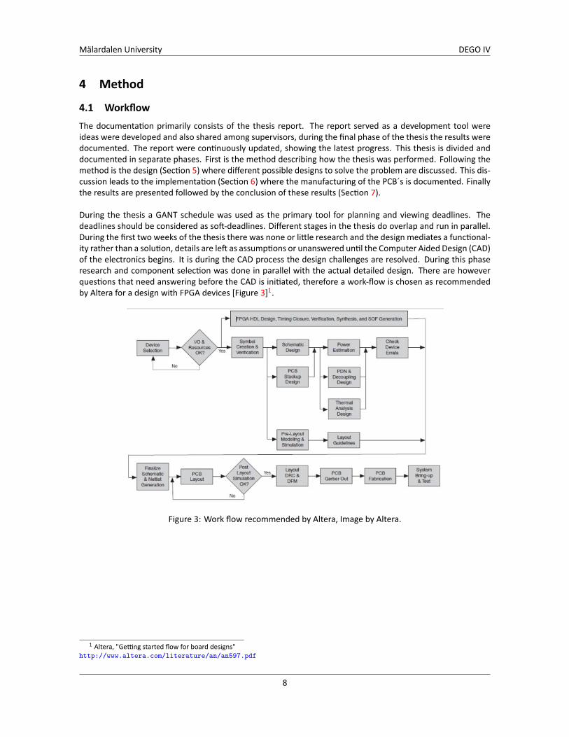
During the thesis a GANT schedule was used as the primary tool for planning and viewing deadlines. Thedeadlines should be considered as so -deadlines. Different stages in the thesis do overlap and run in parallel.During the first two weeks of the thesis there was none or li le research and the design mediates a func onal-ity rather than a solu on, details are le as assump ons or unanswered un l the Computer Aided Design (CAD)of the electronics begins. It is during the CAD process the design challenges are resolved. During this phaseresearch and component selec on was done in parallel with the actual detailed design. There are howeverques ons that need answering before the CAD is ini ated, therefore a work-flow is chosen as recommendedby Altera for a design with FPGA devices [Figure 3]1.
Figure 3: Work flow recommended by Altera, Image by Altera.
1 Altera, "Ge ng started flow for board designs"http://www.altera.com/literature/an/an597.pdf
8
Mälardalen University DEGO IV
The phases can be broken down to:
• Specifica onUnderstanding the current system and new design requirements.
• MethodSe ng up an efficient and construc ve work method.
• DesignMaking a rough new design based on a study of previous work.
• PrototypeA final prototype is to be produced.
• Verifica onVerifying the theore cal design with measurements in the prototype.
• Documenta onIn the documenta on phase the thesis work is more clearly described and edited.
• Presenta onIn the last phase a thesis presenta on is prepared and presented.
4.2 State of the art• Programmable
Making hardware se ngs controllable turns the focus to programmable hardware such as Field Pro-grammableGateArrays (FPGA), Field ProgrammableAnalogArrays (FPAA) and Field ProgrammableMixedsignal Arrays (FPMA) [8]. Other less advanced but efficientmethods are digital poten ometers andMOS-FETs implemented as switches.
FPGAs have been in use for some me in systems where there is a need for either signal adapta onor hardware changes. FPGA technology is also ideally for running data processing in parallel. "An FPGAis a key component that is frequently used in complex system designs because of its programmable na-ture and integrated high-speed transceivers. Because of this flexibility FPGAs have become the centralpart of a flexible system, allowing designers to easily bridge different technologies and u lize both highand low speed signal processing." 2. In these environments the FPGA have proven to be highly func onaland there is an op on to run a so -core (an emulated central processing unit). In the DEGO IV there is aneed to simplify the electronics design and to make the hardware modular.
Preliminary inves ga ons into FPGA technology for the DEGO IV were made resul ng in a selec on oflanguage, tools, program structure and code. Very High speed integrated circuit hardware Descrip onLanguage (VHDL) was selected as the primary programming language (Hardware describing language)and Quartus became the chosen pla orm. A so -core system was setup to run so ware and IP compo-nents for hardware accelerated func ons. A FPMA seems to be advantageous compared to the FPGAbut it is not yet commercially feasible.
• Auto-calibra onThe ambi on is to produce the DEGO IV without the need of manual calibra on. There are different typeof basic circuitry that react and change the hardware to compensate offsets. Digital poten ometers orMOSFETs (floa ng gate transistors) are examples. In spite of the calibra on method there will be a needfor a control loop measuring the circuit state like a redundant sensor [12] or measurement of current
2 Altera, "Ge ng started flow for board designs"http://www.altera.com/literature/an/an597.pdf
9
Mälardalen University DEGO IV
and voltage. Using programmable hardware simplifies hardware calibra on, where FPMA creates a greatpla orm for measuring and adap ng circuitry even during run me.
• Measurement of iner aOne of the requirements of the DEGO IV is to measures the angular posi on of the ship. This is achievedby installing the sensors such as accelerometers and gyroscope directly on the circuit board. WhereAccelerometers measures the proper accelera on, gyroscope measures the angular velocity. There aredifferent types of sensors such as mechanical-, piezoresis ve-sensors. The piezoresis ve sensors are incommon use, where the MEMS based sensors have great advantages [9]. It is possible to determineboth accelera on and angular velocity by using accelerometers [12]. This provides an accurate readingfor a lower implementa on cost.
• Safety cri cal aspectsThere are hardware and so ware requirements to ensure safe opera on. A system is defined as safetycri cal if a failure results in injuries of people, large damage to property or if lifes are at risk. There areaspects to be considered to maintain data integrity and system func onality in the safety cri cal system.A system not accep ng a single point failure causing a cascading common mode failure without redun-dancy could be considered to be a "weak system". These "weak systems" aremore simple thus less proneto failure [3].
To ensure safety or to achieve redundancy there are somewell knownmethods available. Fault-containmentregions providing galvanic isola on to counteract cascading failure and interference. [3], Clock andpower monitoring should be considered as a fundamental necessity [4].
To ensure correct processing of data within the processing unit there could be implementa ons of suchmethods as triple modular redundant architecture or dual lock step architecture that can ensure correctdata processing by comparing the results [3]. Another important aspect in a mul -node system are thebuses. There are many different bus standards such as Controlled Area Network (CAN), Ethernet, RS-485, SAFEbus, SPIDER, TTL and many more. The later men oned buses (SAFEbus, SPIDER, TTL) are medriven buses that are more suitable for safety cri cal applica ons [11]. An interes ng selec on is theSPIDER op cal bus, with its fully electromagne c immunity. If a fault is detected an alarm should relaythis informa on to the user and the system should a ain a safe state as soon as possible.
4.3 So wareThere were some queries regarding the pla orm andwork environment in the beginning of the thesis. Quartusand VHDL were already determined as the pla orm and language for the hardware describing code. For theelectrical CAD there were some alterna ves inves gated, EagleCAD, Ul board and PADS. A er evalua ng theop ons and tes ng the interfaces PADS from Mentor Graphics was selected as the development tool. PADSwas selected due to its compa bility towards quartus. The user interface and simula on capabili es seemedvery good in both Ul board and PADS. Ul board is easily interfaced to Labview however PADS seems to havebe er thermal analysis, which would render them as equal.
4.4 Thesis outputDuring the thesis the components defined in the thesis specifica on (Appendix C) is to be delivered. A report,a prototype and the func on is included in this specifica on.
10
Mälardalen University DEGO IV
5 Design
5.1 ArchitectureThe system func onality and layout is based on a design with low level of details. The top level design isthen developed into more details during the research process. Some general proper es are important for thefunc onality of the overall design. Resistors and capacitors are set to a size of 0603 as recommended by man-ufacturer, this package is small and does not increase expenses nether does it render the targeted tolerancevalues difficult to reach [6].
The dielectric proper es are set to X7R for ceramic capacitors, resistors should be metal film or Metal foildue to their good temperature coefficients [14]. Size and dielectric property of components may vary in spe-cific cases. Tradi onal fuses are not to be used, they are replaced by thermistors due to their auto-rese ngproper es.
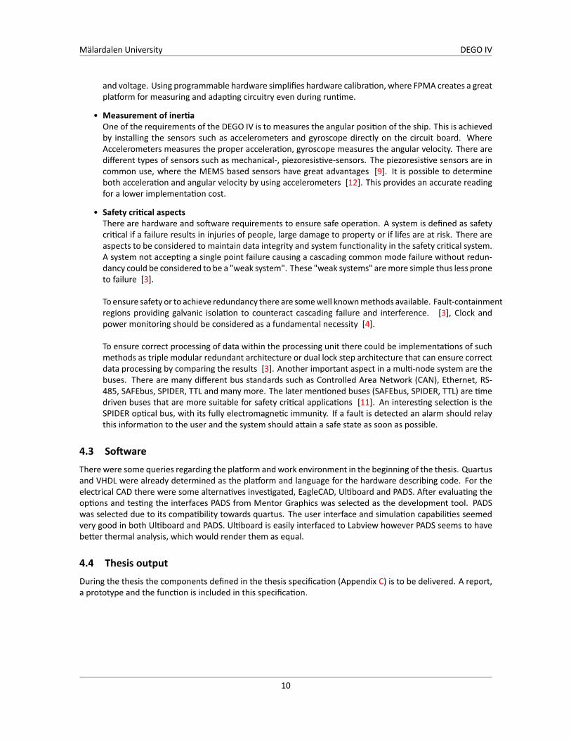
The DEGO IV system must have compa ble specifica ons to the DEGO III system (Appendix E). It is also im-portant to make the system easy to install and maintain. There are jumpers and pins in the DEGO III systemthat are designed for manual measurement, calibra on and setup. These pins have to be removed to sim-plify the manufacturing and procedures during installa on, without losing func onality or safety. The PCB isdesigned to maintain symmetry and electrical soundness according to reference documents on the subject 3.Trace length compensa on have to be considered in some of the high speed buses 4. To get a good overviewof the en re system a high level architecture block diagram was constructed [Figure 4]. General condi ons arebased on the IPC2221 standard5 as in the case of layer stackup in a four layer PCB [Figure 5] or a six layers PCB[Figure 6].
Figure 4: Block diagram of the FPGA system including interface and support func ons.
3David, L , J, "PCB Design Tutorial"http://alternatezone.com/electronics/pcbdesign.htm
4Texas instruments,"High Speed PCB Layout Techniques"http://www.ti.com/lit/ml/slyp173/slyp173.pdf
5The Ins tute for Interconnec ng and Packaging Electronic Circuits, "Generic Standard on Printed Board Design"http://www.mcuexamples.com/Downloads/ipc2221.pdf
11

Mälardalen University DEGO IV
Figure 5: A four layer cross sec on of the governor PCB.
Figure 6: A six layer cross sec on of the governor PCB.
For connec ng the different layers there are via connec on. There are different types of vias [Figure 7]where the vias are copper filled microvias. The A, B and F Vias were selected for connec ng the layers andsupplying power. The vias can be placed directly in pads increasing the rou ng op ons and giving short pathsto ground for decoupling and integrated circuits.
Figure 7: A set of different vias(mm).
12
Mälardalen University DEGO IV
5.2 Power supplyThe system will be fed by a 18V - 32V direct current supply. This voltage is to be broken down into a number ofdiscrete power levels: 24V, 15V, -15V, 12V, 10V, 5V, 3.3V, 2.5V and 1.2V. In DEGO III there are exis ng powersolu ons for some of these power levels. The solu on in DEGO III for fault monitoring the power levels andprotec on from transients is accepted as it is with some reduc ons (see 5.11.2). There are concerns regardingheat and efficiency in some of the voltage regulators. The LM2574 regulator is accepted as a regulator withgood efficiency. The linear LM317L regulator and the in house developed step-down regulator for -15V is notaccepted due to inefficiency on one hand and large amount of components on the other. The linear regulatoris replaced with a LM2574 and the -15V will be regulated by the use of a integrated circuit (IC) TPS84259, thisIC was released a couple of months ago (September, 2012). TPS84259 is an inverter with a wide range of inputvoltage and an output wa age of 15W. The TPS84259 does not require any external magne c components andonly uses five passive external components giving a very low implementa on cost.
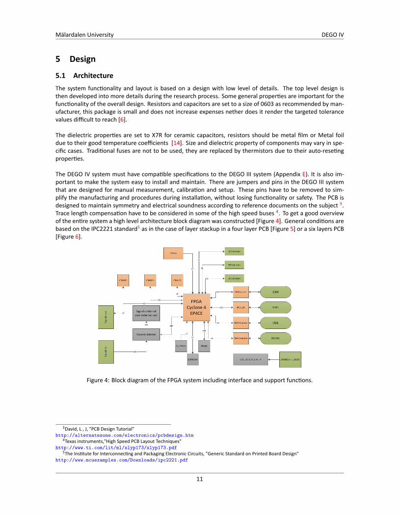
An early power es ma on showed low power requirements below 300mA for the FPGA [Figure 10], opto-cuplers of 200mA, control circuity use of 100mA and inputs and outputs of 1500mA, giving a total power re-quirement of 2,1A at different voltage levels. The TRACO DC-DC voltage converter for 12V supports galvanicisola on and deliver approximately 1A. Within the galvanic isola on area switching regulators regulate thepower. To ensure a stable power supply to the FPGA some Low-Pass Filters (LPF) are introduced to the design.The filters were calibrated and simulated to remove harmful harmonics [Simula on:Appendix B].
An important part to protect the system from interference is to filter the main power. There are inductorsfor such filters, evalua on of the current solu on showed poten al for improvement. A flat wire inductor hasbe er proper es than a round wire one with a compact area, but the largest improvements are AC effec ve-ness, such as lower skin effect resul ng in a be er use of the copper cross sec on. Therefore there is li ledifference using a flat-wire inductor or a round-wire inductor in a DC applica on. A common-mode inductorwith a sec onal winding filters both differen al and common-mode interference effec vely and is thereforethe best selec on.
Figure 8: Quartus thermal and power analysis.
13

Mälardalen University DEGO IV
5.3 FPGAMany aspects of the FPGA are evaluated. Standardized solu ons are to be used as far as possible and referencedesigns will be incorporated into the design within copyright restric ons. The FPGA to be used is the CycloneIV with FLASH, SRAM and a EEPROM. Design considera ons were made according to Altera and ISSI. 6 Hotspots should be avoided to reduce failures from thermo-stress. Proper design is important at the BGA chip toavoid mechanical cracking in pads and vias [10]. 55% of PCB failures in aircra s are the result of overhea ngor thermal-aging according to Dave Steinberg [13]. This makes Thermal related ques ons the first priority forlife expectancy. " A satellite in orbit around the Earth experiences a thermal cycle about every 90 minutes. In20 years it can accumulate about 117,000 thermal cycles." Dave Steinberg. Making on site repairs is unprac-cal, the maintenance is limited to replacing the DEGO IV, a recommended opera on me of the DEGO IV is
considered to be FPGA life me.
5.3.1 Memory set up
The selected memory set-up was chosen due to its simplicity. A 2 MB SRAM was selected as-well as a I2C EEP-ROM 512Kbmemory. For the FPGA image and program code a 8MB Flashmemory was added. The programingis done in Ac ve Serial Mode (ASM) by an Altera USB-blaster. A Serial Configura on Device (EPCS) is used, theEPCS then transfers the FPGA image during power up. During normal use the power up could be calculatedbased on the configura on me7 of the FPGA. The configura on me can be calculated [Equa on 1], the DEGOIV has 1 Bit/Clk.
DataSize ∗ ClkMax
Bit/Clk= NanoSeconds (1)
5.3.2 Decoupling capacitors
Decoupling for the FPGA is a complicated task yet very important. To make a good es mate of the decouplingone needs good informa on of the system impedances (Z) and the maximum allowed system impedance (Z-max) Z must at all mes be lower than Z-max [Equa on 2]. To determine The Z-max one needs to know themaximum current used by the system as well as allowable the AC ripple in percentage. For a FPGA these valuesare available in the documenta on. The Z-max is calculated [Equa on 3], [1]. The system impedance is verydifficult to calculate but can be well es mated if parasi c effects on the impedance are kept to a minimum dueto good PCB layout. If the clk is considered as the fundamental harmonic and the rest of the harmonics can beignored and the decoupling can be es mated [Equa on 4].
A supplement method to compensate for changes in the impedance could be to place the resonances fre-quency of the decoupler capacitors with parasi c effects [Equa on 5] to cancel resonant frequency of theparasi c effects from trace induc on and die capacitance [Equa on 6]. There is an illustra on to view theidea of this hypothesis [Figure 9]. It is important to remember that inductance reverses its effects a er theopera ng frequency passes the self-resonance of the system [15].
6These recommenda ons include but are not limited to documents such asAltera, " Cyclone IV Schema c Review Worksheet",http://www.altera.com/download/board-layout-test/schematic-review-ws/worksheets/Cyclone_IV_Schematic_Review_Worksheet.docAltera, "CycloneIV Device Family Pin Connec on Guidelines",http://www.altera.com/literature/dp/cyclone-iv/PCG-01008.pdfAltera, "Cyclone IV Device Handbook",http://www.altera.com/literature/hb/cyclone-iv/cyclone4-handbook.pdf.Altera, "I/O Management",http://www.altera.com/literature/hb/qts/qts_qii52013.pdf.
7Altera,"Serial Configura on (EPCS) Devices Datasheet"http://www.altera.com/literature/hb/cfg/cyc_c51014.pdf
14

Mälardalen University DEGO IV
The previously men oned parasi c effects indicate to be the most influen al ones [1]. Other factors can how-ever be added to this calcula on to increase accuracy. For instance the plane capacitance can be added, and soon for be er results. Finally measurements on a prototype has to be done to answer if the systems impedanceis properly within the limit of Z-max. For the DEGO IV Z-max is 252mΩ for the internal power (VCCINT) of theFPGA.
Zmax > Z (2)
Zmax =
[V oltageRail
Ripple
MaxTransientCurrent
](3)
C =
[1
F∗Z2π
](4)
F =1
2π√Lcap ∗ Ccap
(5)
F =1
2π√(Ltrace+ Lpackage) ∗ Cdie
(6)
Figure 9: Impedance curves
15
Mälardalen University DEGO IV
5.4 Input and outputInput and output design will strive for an uniform solu on. Any adap on or filtering of one specific signal willbe processed within the FPGA. These changes are all in the line with ambi on to simplify the hardware archi-tecture. Signals do have some differences. Signals are therefore divided into different categories. Transientprotec on on I/O was first selected to consist of scho ky-diodes and zener-diodes but on recommenda onfrom an adviser this was changed to a transient voltage suppression diode due to high power absorp on andthe good property that in the case of breakdown they goes to short circui ng thus protec ng the circuitry.
5.4.1 Digital inputs
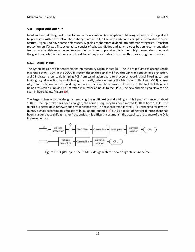
The system has a need for environment interac on by Digital Inputs (DI). The DI are required to accept signalsin a range of 0V - 32V. In the DEGO III system design the signal will flow through transient voltage protec on,a LED indicator, cross cable jumping PCB from termina on board to processor board, signal filtering, currentlimi ng, signal selec on by mul plexing then finally before entering the Micro-Controller Unit (MCU), a layerof galvanic isola on. In the new design a few elements will be removed. This is due to the fact that there willbe no cross cable jump and no limita on in number of inputs to the FPGA. The new and old signal flow can beseen in figure below [Figure 10].
The largest change to the design is removing the mul plexing and adding a high input resistance of about100kΩ. The input filter has been changed, the corner frequency has been moved to 1KHz from 10kHz. Thefiltering is be er despite fewer and smaller capacitors. The response me for the DI is unchanged for low fre-quency signals according to simula ons [Simula on:Appendix B] but as a result of heavier filtering there hasbeen a larger phase shi at higher frequencies. It is difficult to es mate if the actual step response of the DI isimproved or not.
Figure 10: Digital input: the DEGO IV design with the new design structure below.
16
Mälardalen University DEGO IV
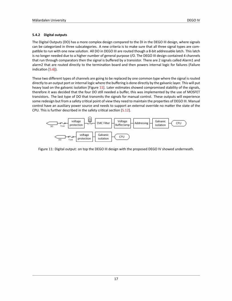
5.4.2 Digital outputs
The Digital Outputs (DO) has a more complex design compared to the DI in the DEGO III design, where signalscan be categorized in three subcategories. A new criteria is to make sure that all three signal types are com-pa ble to run with one new solu on. All DO in DEGO III are routed though a 8-bit addressable latch. This latchis no longer needed due to a higher number of general purpose I/O. The DEGO III design contained 4 channelsthat run through comparators then the signal is buffered by a transistor. There are 2 signals called Alarm1 andalarm2 that are routed directly to the termina on board and then powers internal logic for failures (Failureindica on [5.6]).
These two different types of channels are going to be replaced by one common type where the signal is routeddirectly to an output port or internal logic where the buffering is done directly by the galvanic layer. This will putheavy load on the galvanic isola on [Figure 11]. Later es mates showed compromised stability of the signals,therefore it was decided that the four DO s ll needed a buffer, this was implemented by the use of MOSFETtransistors. The last type of DO that transmits the signals for manual control. These outputs will experiencesome redesign but from a safety cri cal point of view they need to maintain the proper es of DEGO III. Manualcontrol have an auxiliary power source and needs to support an external override no ma er the state of theCPU. This is further described in the safety cri cal sec on [5.12].
Figure 11: Digital output: on top the DEGO III design with the proposed DEGO IV showed underneath.
17
Mälardalen University DEGO IV
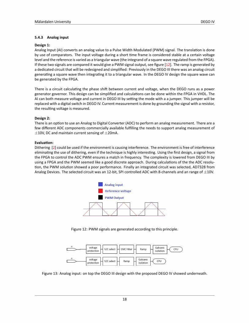
5.4.3 Analog input
Design 1:Analog Input (AI) converts an analog value to a Pulse Width Modulated (PWM) signal. The transla on is doneby use of comparators. The input voltage during a short me frame is considered stable at a certain voltagelevel and the reference is varied as a triangular wave (the integrand of a square wave regulated from the FPGA).If these two signals are compared it would give a PWM signal output, see figure [12]. The ramp is generated bya dedicated circuit that will be redesigned and simplified: Previously in the DEGO III there was an analog circuitgenera ng a square wave then integra ng it to a triangular wave. In the DEGO IV design the square wave canbe generated by the FPGA.
There is a circuit calcula ng the phase shi between current and voltage, when the DEGO runs as a powergenerator governor. This design can be simplified and calcula ons can be done within the FPGA in VHDL. TheAI can both measure voltage and current in DEGO III by se ng the mode with a a jumper. This jumper will bereplaced with a digital switch in DEGO IV. Current measurement is done by grounding the signal with a resistor,the resul ng voltage is measured.
Design 2:There is an op on to use an Analog to Digital Converter (ADC) to perform an analog measurement. There are afew different ADC components commercially available fulfilling the needs to support analog measurement of±10V, DC and maintain current sensing of±20mA.
Evalua on:Dithering [2] could be used if the environment is causing interference. The environment is free of interferenceelimina ng the use of dithering, even if the technique is highly interes ng. Using the first design, a signal fromthe FPGA to control the ADC PWM ensures a match in frequency. The complexity is lowered from DEGO III byusing a FPGA and the PWM seemed like a good discrete approach. During calcula ons of the the ADC resolu-on, the PWM solu on showed a poor performance. Finally an integrated circuit was selected, AD7328 from
Analog Devices. The selected circuit was an 12-bit, SPI controlled ADC with 8-channels and an range of±10V.
Figure 12: PWM signals are generated according to this principle.
Figure 13: Analog input: on top the DEGO III design with the proposed DEGO IV showed underneath.
18
Mälardalen University DEGO IV
5.4.4 Analog output
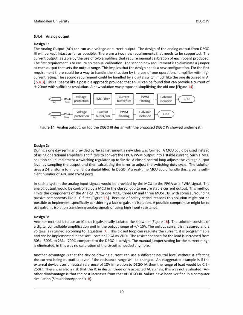
Design 1:The Analog Output (AO) can run as a voltage or current output. The design of the analog output from DEGOIII will be kept intact as far as possible. There are a two new requirements that needs to be supported. Thecurrent output is stable by the use of two amplifiers that require manual calibra on of each board produced.The first requirement is to ensure nomanual calibra on. The second new requirement is to eliminate a jumperat each output that sets the output range. This implies that the design needs a new configura on. For the firstrequirement there could be a way to handle the situa on by the use of one opera onal amplifier with highcurrent ra ng. The second requirement could be handled by a digital switch much like the one discussed in AI( 5.4.3). This all seems like a possible approach provided that an OP can be found that can provide a current of± 20mA with sufficient resolu on. A new solu on was proposed simplifying the old one [Figure 14].
Figure 14: Analog output: on top the DEGO III design with the proposed DEGO IV showed underneath.
Design 2:During a one day seminar provided by Texas instrument a new idea was formed. A MCU could be used insteadof using opera onal amplifiers and filters to convert the FPGA PWM output into a stable current. Such a MCUsolu on could implement a switching regulator up to 5MHz. A closed control loop adjusts the voltage outputlevel by sampling the output and then calcula ng the error to adjust the switching duty cycle. The solu onuses a Z-transform to implement a digital filter. In DEGO IV a real- me MCU could handle this, given a suffi-cient number of ADC and PWM ports.
In such a system the analog input signals would be provided by the MCU to the FPGA as a PWM signal. Theanalog output would be controlled by a MCU in the closed loop to ensure stable current output. This methodlimits the components of the Analog I/O to one MCU, three OP and three MOSFETs, with some surroundingpassive components like a LC-filter [Figure 15]. Because of safety cri cal reasons this solu on might not bepossible to implement, specifically considering a lack of galvanic isola on. A possible compromise might be touse galvanic isola on transfering analog signals or using high input resistance.
Design 3:Another method is to use an IC that is galvanically isolated like shown in [Figure 16]. The solu on consists ofa digital controllable amplifica on unit in the output range of +/- 15V. The output current is measured and avoltage is returned according to [Equa on 7]. This closed loop can regulate the current, it is programmableand can be implemented in the so - core or FPGA as VHDL. The resistance span for the load is increased from50Ω - 500Ω to 25Ω - 700Ω compared to the DEGO III design. The manual jumper se ng for the current rangeis eliminated, in this way no calibra on of the circuit is needed anymore.
Another advantage is that the device drawing current can use a different neutral level without it effec ngthe current being outpu ed, even if the resistance range will be changed. An exaggerated example is if theexternal device uses a neutral reference of 10V in rela on to DEGO IV, then the range of load would be 0Ω -250Ω. There was also a risk that the IC in design three only accepted AC signals, this was not evaluated. An-other disadvantage is that the cost increases from that of DEGO III. Values have been verified in a computersimula on [Simula on:Appendix B].
19
Mälardalen University DEGO IV
Design 4:The last evaluated method was to use a biased transistor to regulate the current output. This solu on did notsa sfy the±20mA but delivered only a 20mA current.
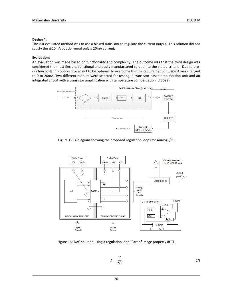
Evalua on:An evalua on was made based on func onality and complexity. The outcome was that the third design wasconsidered the most flexible, func onal and easily manufactured solu on to the stated criteria. Due to pro-duc on costs this op on proved not to be op mal. To overcome this the requirement of±20mA was changedto 0 to 20mA. Two different outputs were selected for tes ng, a transistor based amplifica on unit and anintegrated circuit with a transistor amplifica on with temperature compensa on (LT3092).
Figure 15: A diagram showing the proposed regula on loops for Analog I/O.
Figure 16: DAC solu on,using a regula on loop. Part of image property of TI.
I =V
80(7)
20

Mälardalen University DEGO IV
5.4.5 Tacho input
The Tacho inputs of the DEGO III are well designed. With the FPGA technology we acquire the op on to movesome func onality from digital electronics to the VHDL hardware descrip on. This enables us to eliminate thefrequency divider and jumpers. The current and voltage transient protec on including hysteresis protec oncan be kept from the DEGO III design.
5.5 Galvanic isola onThere are several op ons for galvanic isola on where opto-couplers or induc ve iCouplers are the two primaryselec ons. There are some criterias to fulfill:
• Preferably they should be in PCB manufactures stock as a standard component.
• There should be several IC manufactures.
• All isolators should be of the same type and part number.
• Frequency supported has to be at least 13,5kHz.
• Long life expectancy.
The first two points were fulfilled by the opto-coupler but the other requirement are be er met by the Icouplerwith a life expectancy of 50 years and with higher opera onal frequency. A opto-coupler can handle a largevoltage as long as the current is limited. The Icoupler needs a fixed voltage of 2V to 5V and good flanks to work.Icoupler was selected due to its speed and life expectancy.
5.6 Failure indica onThe failure indica on on DEGO III is simple yet very effec ve. The func on is based on solid state relays. DEGOIII uses an Array of NOT-gates for handling signal switching in a very cunning way. One could say it is a smallpiece of engineering art, sadly it increases the complexity of the board and it is therefore removed. DEGO IVuses the solid-state relay func on controlled directly by a control signal.
5.7 Digital selec onIn order to use dual func onality of some func ons like AI (voltage/current) or the voltage regulator se ng(fixed/adjustable), a hardware selector was needed. Currently manual jumpers are used, these should be re-placed with digital switches. Different requirements exist depending on the loca on of the switch. PrimarilyMOSFETs would be used as switches for the simplicity and low price. If a transistor should be used as a switchit should not operate in its ohmic state, but move as fast as possible from sub-threshold [Equa on 8] to ac vemode [Equa on 9]. It is important that the MOSFET construc on fulfills these requirements to work properly.In some parts of the system a n-channel MOSFET is needed to power a P-Channel MOSFET. In some placesthe condi ons are insufficient to use one or two simple MOSFETs. In these places solid-state relays have beenused. Switches have been simulated to ensure the func on and response me before manufacture. By thesesimula ons, phase shi has been minimized [Appendix B].
V gs < V th (8)
(V ds > V gs− V th) ∩ V gs > V th (9)
21
Mälardalen University DEGO IV
5.8 External Interface and busesDEGO IV requires interfaces to be func onal. These peripherals include the digital and analog I/O for backwardcompa bility. There are also more complex interfaces necessary for normal opera on. There are interfacesnecessary during run me and there are some needed for debugging and programming. Also Some buses forinternal rou ng on the PCB and some buses that interact with external devices are required.
5.8.1 Debug op ons
There is a need to debug the system in development and in normal opera on. Themain debugging is to be doneby the use of an USB link, secondary debugging is done by a on-board 20 x 4 display with a parallel interface.In the future a touchscreen can serve as an on-board control interface (sec on 5.9). This might even eliminatethe need for a PC if the user wants a more integrated solu on.
5.8.2 Ethernet
Ethernet is a collec on of standardizedmethods for data communica on. DEGO IV is designed for compa bilitywith IEEE 802.3 8 . This is implemented by the use of a Phyceiver handling the physical layer by communica ngby ReducedMedia Independent Interface (RMII). Originally a DMA9000Awas intended to be used. This chip in-cludes the Sublayer forMedia Access Control (MAC). The DMA9000A simplifies the so ware but limits the user.The design is verified to support 100BASE- TX. Ji er dampening and galvanic isola on necessary by IEEE802.3is integrated in the RJ-45 Connector and supports BASE 1000 opera ons. DMA9000A was later replaced witha TI DP83848I.
5.8.3 RS485
The system needs two RS485 ports using a transceiver that connects to the bus. The connec on uses zener-diodes and filtering capacitors to sa sfy standards. The impedance in the transceivers is considered as veryhigh and Pull-down resistors have been added. The transceivers (ADM2682E) are powered by the DEGO IVlocally and are galvanically isolated.
5.8.4 CAN
The CAN connec on uses an isolated transceiver ADM3053. The design is equipped with protec ve circuitryand filtering by use of a commonmode filter. The differen al pair have transient protec on by the use of zener-diodes that protect CAN-H and CAN-L from over +5V and nega ve voltage. Originally a digital switch would givea programmable op on to operate the transceiver on bus power or internally regulated power. Using the on-board power would effec vely interfere with the galvanic isola on. ADM3053 has a built in isolated DC-DCconverter without an increased IC cost giving no disadvantage opera ng the CAN on a three wire interface.The construc on principle used is in line with normal praxis.
5.8.5 I2C
As described by the I2C specifica on9 this bus works as an addressed serial communica on link. There arethree buses available on the board, EEPROM uses one of these buses. Two buses are connected to externalconnectors resul ng in up to twenty op onal external devices can added to the system. The buses includepull-ups for data lines and series resistors to the devices according to I2C specifica on. The values for resistorsin the external units are calculated according to 20 connected nodes. External units should use a 100Ω resistorin series on the CLK and data line to reduce noise while opera ng with twenty connected nodes. The I2C busis configured for 3.3V devices.
8IEEE, "IEEE 802.3: ETHERNET"http://standards.ieee.org/about/get/802/802.3.html
9Department of computer science, University of North Carolina, "The I2C-bus Specifica on"http://www.cs.unc.edu/Research/stc/FAQs/Interfaces/I2C-BusSpec-V2.1.pdf
22
Mälardalen University DEGO IV
5.8.6 Serial Peripheral Interface Bus
There are several peripherals in the system that are using a Serial Peripheral Interface Bus (SPI). The SPI is afour signal bus. Three buses are available for gyroscopes and two buses are reserved for ADC. There is one busextended to a connector for external use.
5.8.7 USB
This interface was kept simple, an USB controller from FTDI UART- USB was selected. The communica on tothe controller is a standard UART with signal pins RTS and CTS. Common mode filter was added to filter datalines but no external protec ve circuitry was added. The controller is internally powered from the board. Therequirements for an USB self powered configura on are met10.
5.9 Touch interface/screenThere must be a method for interfacing and displaying output from the DEGO IV. To keep up with currenttechnology and to make the interface user-friendly it has been decided that a touch-screen interface would bea good solu on. It is not within the scope of this thesis to design this interface. What is part of this thesis is toperform the necessary ac ons to allow this interface to be added at a later phase without the need to makedesign changes to the PCB. From discussions with consul ng a expert it was decided that I2C (Sec on 5.8.5) orSPI (Sec on 5.8.6) was a suitable hardware interface for this touchscreen. Another cost-effec ve and flexiblesolu on is to set up wireless access-points to interface tablets to ship control. DEGO IV will also support an4x20 dot matrix display on a parallel and serial interface.
5.10 Iner a measurementBased on the report by Christer Gerdtman et al. [7] good results of measuring quick movements was achievedby using gyroscopes in two axis. The MEMS based mouse in the paper operated using a CG-L43 NecTokingyroscope. CG-L43 was for the DEGO IV unsuited due to the fact that there is a need for measurement in threeaxis with devices mounted on a PCB. A good alterna ve is the CRM200 Pin point and CRM100 Pin Point with itsgood performance and small size. These would measure rota onal speed very well, but due to the gyroscopesquality, the cost is high. There is an alterna ve solu on to use accelerometers that are cheaper and easierto acquire. It will require more work to get reliable rota onal data from these devices, but it is possible withfiltering to acquire similar results.
5.11 Autonomous func onalityThe DEGO IV system is designed to require low knowledge for the installa on and maintains. To ensure safeopera on there is a need for autonomous func ons that can test, monitor and calibrate the system. This willalso lower produc on me and -cost as well.
5.11.1 Automa c tes ng
The first factor is to ensure correct func onality of the system, this includes both so ware and hardware. Test-ing can be divided into two parts where one is pure electrical (measurements) and a second is system behavior(logic). System behavior can be verified by connec ng the system to a test suit, simula ng all inputs and gen-era ng digital records of the test as described by Li Zhiming, Jiao Jian and Xu Guozhi [16]. Such a test wouldbe a very useful tool in produc on but could also alert personnel to poten al problems during run me [5].This is not in the scope of this thesis, however there are hardware requirements for this func onality that are
10 FTDI, "FT232R USB UART IC Datasheet"http://www.ftdichip.com/Support/Documents/DataSheets/ICs/DS_FT232R.pdfl
23

Mälardalen University DEGO IV
important to implement. To ensure hardware compa bility the electrical setup must support voltage mea-suring, at some points, to evaluate signal integrity. Appropriate posi ons for theses test points could be thepresent manual test points (see sec on architecture 5.1), the measured signal could also handle autonomouscalibra on(5.11.2). Complexity of the circuit would increase, therefore a decision was made not to include thecon nuous system measurement points. Supply monitoring was included in analog circuitry.
5.11.2 Automa c calibra on
During startup and run me measured values could be used to calibrate digital poten ometers to compensatefor inaccuracy in components and temperature varia ons. Using such a discrete solu on complicates the designconsiderably and should be avoided. The best approach would be to use components and design with a highaccuracy and linear behavior to avoid dri .
5.12 Safety cri cal func onalityControlling a ship includes safety cri cal func ons and electronics stability. To ensure correct func onalitythe system could benefit from a AT ny13 micro-controller set up, for a very low cost. This micro-controllercould work as a watchdog with an external reset or as a external clock to give a redundant clock reference.If the system consists of several nodes with communica on, as is normal for this system, then the nodes canfunc on as redundant nodes for each-other.
5.12.1 Manual override
The crew must at all mes be in control of the ship. There is a manual override for the governor in DEGO III,this override contains many discrete components. One of the main objec ves of DEGO IV is to simplify theconstruc on, therefore there is a need to integrate func ons of the override into the so ware or VHDL. Theoverride consists of two bu ons, one for increasing speed and one for reducing speed. These supersede thenormal opera ng parameters and takes control of the engine speed. Integra ng the discrete components mustbemade safely and theremust be an evalua on of system failures, such as a race condi on or a hardware failurein the FPGA. In the current DEGO III design there is a separate power feed of the manual override separa ngit completely from all circuitry in the board level design. Due to the fact of the safety cri cal nature of theproject the removal of discrete logic have been deemed as a high risk. As described previously, different nodesin the system can serve as a redundancy for other nodes. Using this advantage one can eliminate discretecomponents safely without sacrificing safety.
24
Mälardalen University DEGO IV
6 Implementa on
6.1 Computer aided design6.1.1 Components crea on
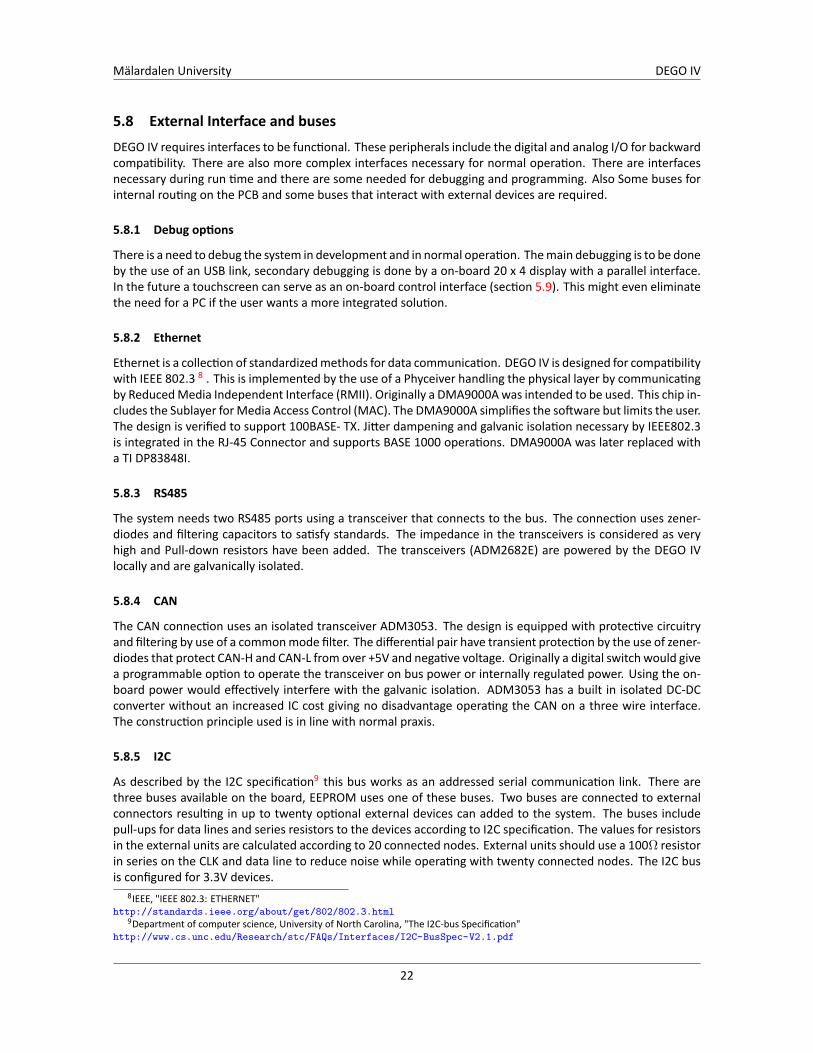
To implement the design there is a need to prepare design components. The largest prepara on is the footprintand the layout schema c of the CAD. As an example, the process of crea ng the FPGA is described. First a Layoutand pin numbering has to be established [Figure 17], then there is a need to establish the func on of each pinand finally howmany pins the design requires. Selec ng pins for the PCB func onality is done by use of Alteraspin specifica on11. Finally the schema cs symbol is created to represent the pins needed for DEGO IV12. Thisprocess is repeated for each component.
Figure 17: The pins are ordered in a numbered sequence 1 to 484
6.1.2 PCB schema c
The design of the schema c is done by a research process. Informa on for design is acquired by such mediaas data-sheets, ar cles, seminars and more (Sec on 5). The design is compiled to a PADS layout documentcreated from scratch.
6.2 Produc on prepara ons6.2.1 Component selec on
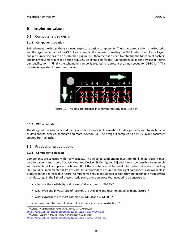
Components are selected with many aspects. The selected components must first fulfill its purpose, it mustbe affordable, it must be a Surface Mounted Device (SMD) [figure 18] and it must be possible to assemblewith available pick and place machines. All of these criteria must be meet. Secondary criteria such as longlife should be implemented if it's possible. It is important to ensure that the right components are available inproduc on for a foreseeable future. Components should be selected so that they are obtainable from severalmanufactures. In the light of these criteria some ques on arose that needed to be answered:
• What are the availability and prices of Altera Low cost FPGA´s?
• What type and physical size of resistors are available and recommended by manufacturer?
• What gyroscopes are most common (CRM100 and CRM 200)?
• Surface mounted complica ons, like if there are picker restric ons?11Altera, "Pin Informa on for the Cyclone® IV EP4CE40 Device"
http://www.altera.com/literature/dp/cyclone-iv/EP4CE40.pdf12Altera, "CycloneIV Device Family Pin Connec on Guidelines"
http://www.altera.com/literature/dp/cyclone-iv/PCG-01008.pdf
25
Mälardalen University DEGO IV
• Prototype considera ons and complica ons such as improper footprint, will these be detected beforeassembly?
• Soldering method, what are the ideal temperatures for soldering?
• Time for comple ng a prototype?
These ques ons and a general discussion of the produc on flow were made during a early-produc onmee ng with the local manufacturer. Giving a produc on me of 4 weeks.
Figure 18: One of the surface mounted components in the design.
6.2.2 PCB Layout
To create the PCB layout, PADS Layout is used. Components are posi oned by hand, longer nets are routed inthe internal layers according to the IPC222113. On superficial layers nets are not allowed to be longer than 3cm as a maximum. The Ball Gate Array (BGA) components require a smooth surface, preferably Surface fin-ish electroless nickel gold. BGA also needs breakout tabs or stacked microvias in the pad. The aspect ra o ofthrough-holes is recommended to 1:6 - 1:8, for a 1.6mm PCB that ends up with 0.55mm - 0.6mm pad leavingsmall tolerance with a fine BGA, 1.0mm pitch. Therefore stacked-microvias is the best op on allowing a max-imized rou ng net. This moves the produc on of the PCB further from the local area to either Germany orChina.
6.3 PrototypeThe process of moving theory to prac ce includes making the physical product. The task of producing theproduct were moved to a third party. The third party needed informa on of physical parameters, to assemblethe final prototype.The informa on included:
• Bill of material
• Pick & place data
• PCB
The Bill Of Materials (BOM) and pick & place data were generated from PADS, and the PCBs were ordered fromGermany. Several itera ons of the BOM were run to match components which were already available at theboardmanufacturer. Unfortunately therewere some issues during themanufacturemaking a foreseeable delayin comple ng a prototype. This resulted in some manual assembly of the circuitry at Mälardalen University.
13The Ins tute for Interconnec ng and Packaging Electronic Circuits, "Generic Standard on Printed Board Design"http://www.mcuexamples.com/Downloads/ipc2221.pdf
26
Mälardalen University DEGO IV
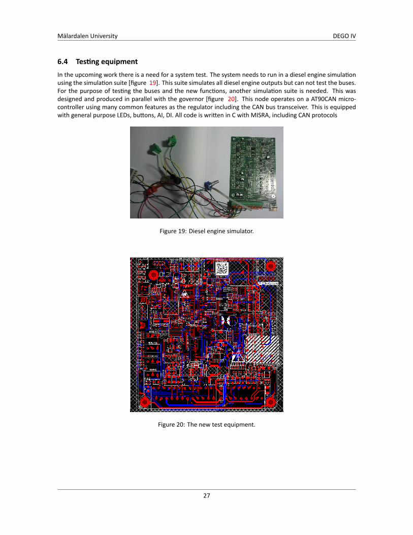
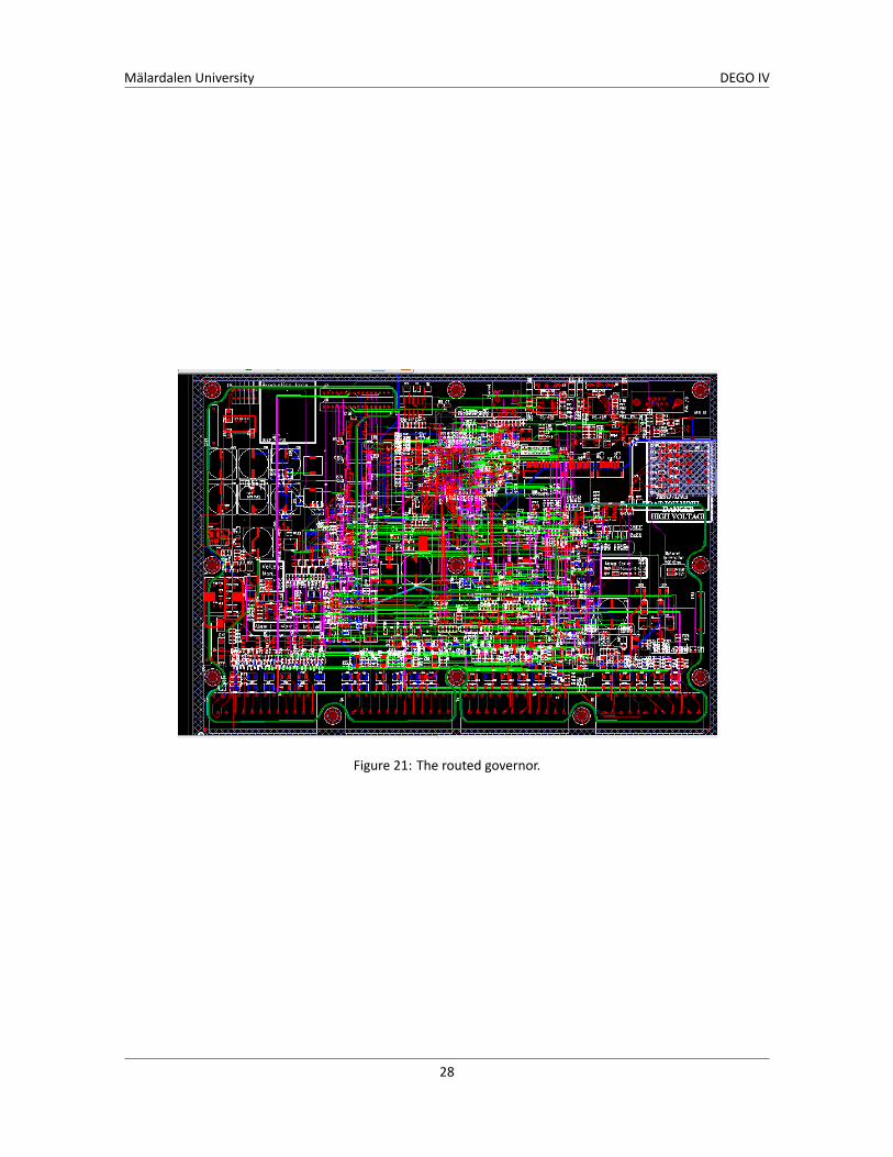
6.4 Tes ng equipmentIn the upcoming work there is a need for a system test. The system needs to run in a diesel engine simula onusing the simula on suite [figure 19]. This suite simulates all diesel engine outputs but can not test the buses.For the purpose of tes ng the buses and the new func ons, another simula on suite is needed. This wasdesigned and produced in parallel with the governor [figure 20]. This node operates on a AT90CAN micro-controller using many common features as the regulator including the CAN bus transceiver. This is equippedwith general purpose LEDs, bu ons, AI, DI. All code is wri en in C with MISRA, including CAN protocols
Figure 19: Diesel engine simulator.
Figure 20: The new test equipment.
27
Mälardalen University DEGO IV
Figure 21: The routed governor.
28
Mälardalen University DEGO IV
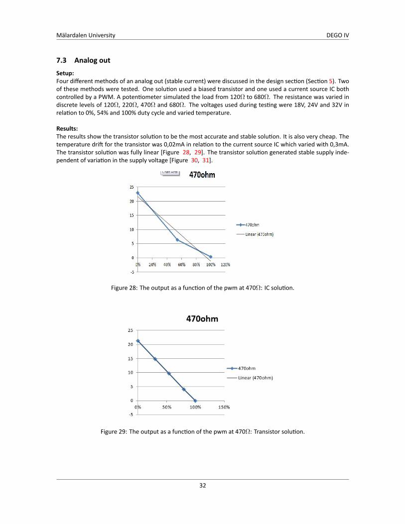
7 Verifica onTo ensure safe opera on and to es mate a life me expectancy the system needs to be tested. Some testsmight be performed in the laboratory [Figure 22, 23] verifying the design and thesis. Other tests are neededto verify system func onality.
Figure 22: Assembled circuit boards.
Figure 23: Work bench setup.
29

Mälardalen University DEGO IV
7.1 Digital outSetup:An external load is connected to digital out. The output then toggles, controlled by the MCU.
Results:The toggling signal passes the galvanic isola on almost unaffected, and the digital output delivers expectedresults.
7.2 Digital inSetup:An external signal is fed to the digital input. The comparator should react and send the signal onwards to theMCU through the galvanic isolators. The signal is 12V with a 2V ripple swept from 0,5Hz to 500kHz. Using thismethod the behavior of the DI can be observed. The step response and signal filtering can be compared tosimula ons.
Results:This func on worked well and there were no complica ons. The filters gave a dampening effect at 5kHz andabove [Figure 24 25], verifying the simula ons (Sec on B). The step response was somewhat be er in thenew solu on [Figure 26, 27] not including the switching me and mul plexing in the older version. The stepresponse was lowered by approximately 15ms altogether.
Figure 24: 40Khz test signal. Blue: before filter. Yellow: a er filter.
Figure 25: 740Hz test signal. Blue: before filter. Yellow: a er filter.
30

Mälardalen University DEGO IV
Figure 26: Step response at 2kHz, new solu on.
Figure 27: Step response at 2kHz, old solu on.
31
Mälardalen University DEGO IV
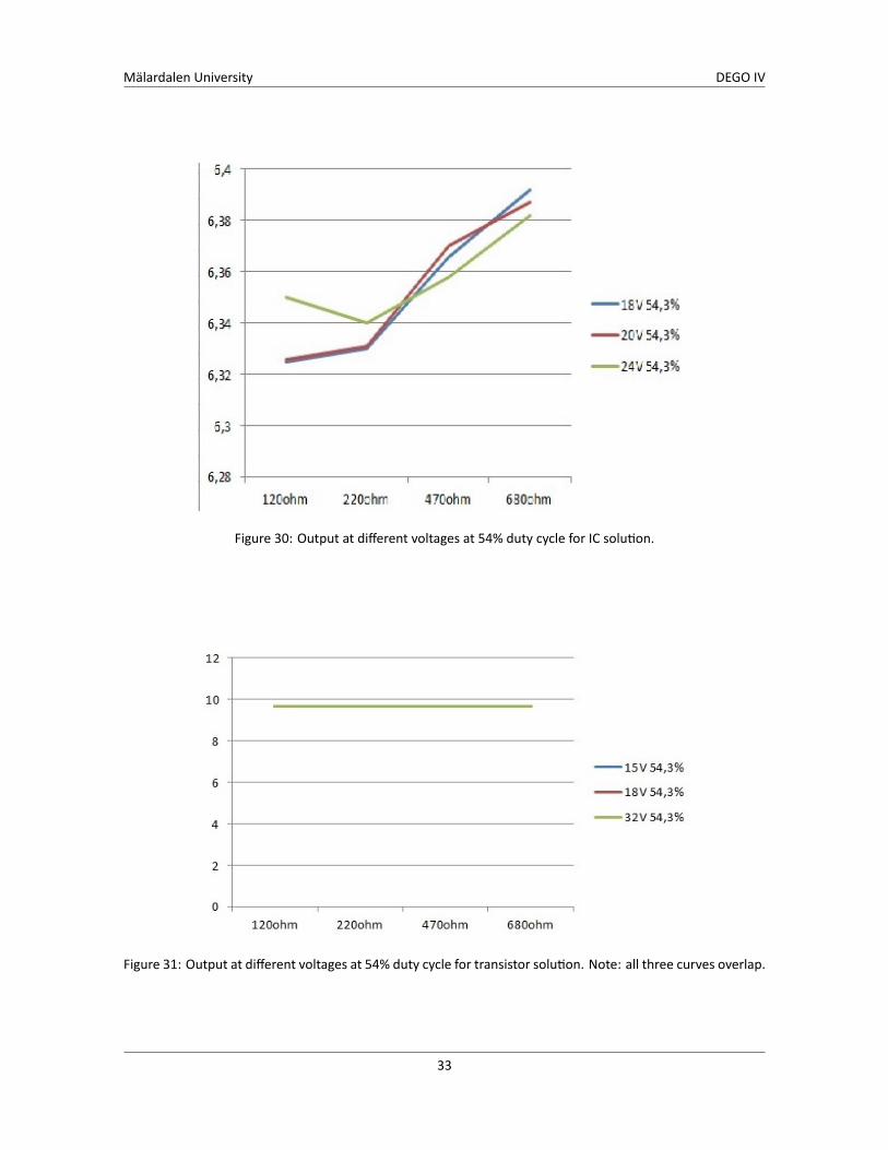
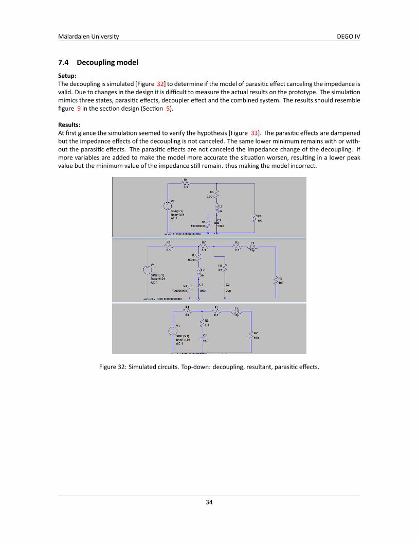
7.3 Analog outSetup:Four different methods of an analog out (stable current) were discussed in the design sec on (Sec on 5). Twoof these methods were tested. One solu on used a biased transistor and one used a current source IC bothcontrolled by a PWM. A poten ometer simulated the load from 120Ω to 680Ω. The resistance was varied indiscrete levels of 120Ω, 220Ω, 470Ω and 680Ω. The voltages used during tes ng were 18V, 24V and 32V inrela on to 0%, 54% and 100% duty cycle and varied temperature.
Results:The results show the transistor solu on to be the most accurate and stable solu on. It is also very cheap. Thetemperature dri for the transistor was 0,02mA in rela on to the current source IC which varied with 0,3mA.The transistor solu on was fully linear [Figure 28, 29]. The transistor solu on generated stable supply inde-pendent of varia on in the supply voltage [Figure 30, 31].
Figure 28: The output as a func on of the pwm at 470Ω: IC solu on.
Figure 29: The output as a func on of the pwm at 470Ω: Transistor solu on.
32
Mälardalen University DEGO IV
Figure 30: Output at different voltages at 54% duty cycle for IC solu on.
Figure 31: Output at different voltages at 54% duty cycle for transistor solu on. Note: all three curves overlap.
33
Mälardalen University DEGO IV
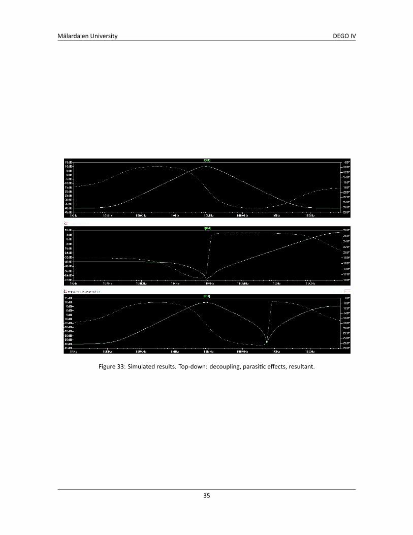
7.4 Decoupling modelSetup:The decoupling is simulated [Figure 32] to determine if themodel of parasi c effect canceling the impedance isvalid. Due to changes in the design it is difficult to measure the actual results on the prototype. The simula onmimics three states, parasi c effects, decoupler effect and the combined system. The results should resemblefigure 9 in the sec on design (Sec on 5).
Results:At first glance the simula on seemed to verify the hypothesis [Figure 33]. The parasi c effects are dampenedbut the impedance effects of the decoupling is not canceled. The same lower minimum remains with or with-out the parasi c effects. The parasi c effects are not canceled the impedance change of the decoupling. Ifmore variables are added to make the model more accurate the situa on worsen, resul ng in a lower peakvalue but the minimum value of the impedance s ll remain. thus making the model incorrect.
Figure 32: Simulated circuits. Top-down: decoupling, resultant, parasi c effects.
34
Mälardalen University DEGO IV
Figure 33: Simulated results. Top-down: decoupling, parasi c effects, resultant.
35
Mälardalen University DEGO IV
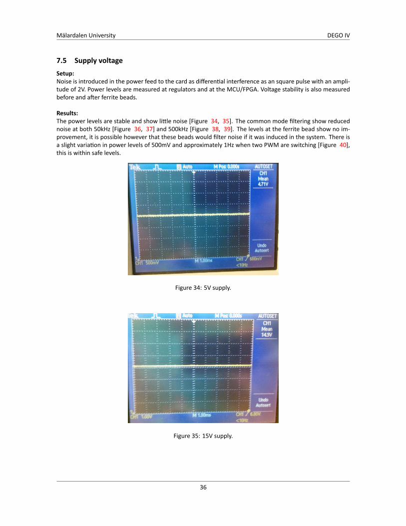
7.5 Supply voltageSetup:Noise is introduced in the power feed to the card as differen al interference as an square pulse with an ampli-tude of 2V. Power levels are measured at regulators and at the MCU/FPGA. Voltage stability is also measuredbefore and a er ferrite beads.
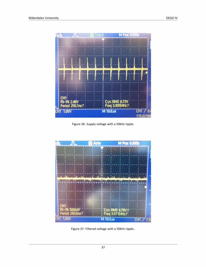
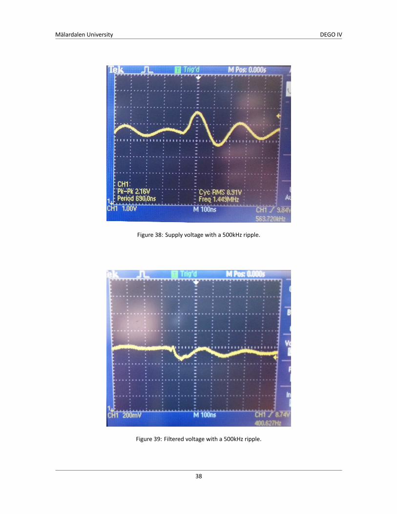
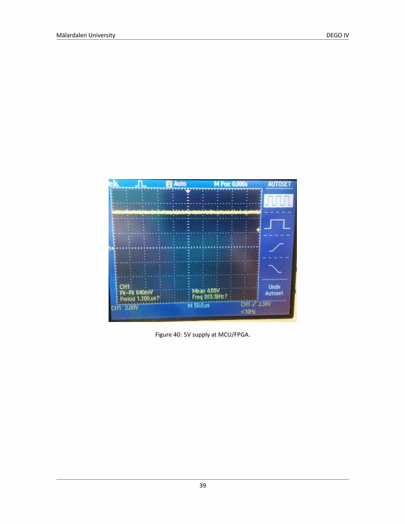
Results:The power levels are stable and show li le noise [Figure 34, 35]. The common mode filtering show reducednoise at both 50kHz [Figure 36, 37] and 500kHz [Figure 38, 39]. The levels at the ferrite bead show no im-provement, it is possible however that these beads would filter noise if it was induced in the system. There isa slight varia on in power levels of 500mV and approximately 1Hz when two PWM are switching [Figure 40],this is within safe levels.
Figure 34: 5V supply.
Figure 35: 15V supply.
36
Mälardalen University DEGO IV
Figure 36: Supply voltage with a 50kHz ripple.
Figure 37: Filtered voltage with a 50kHz ripple..
37
Mälardalen University DEGO IV
Figure 38: Supply voltage with a 500kHz ripple.
Figure 39: Filtered voltage with a 500kHz ripple.
38
Mälardalen University DEGO IV
Figure 40: 5V supply at MCU/FPGA.
39

Mälardalen University DEGO IV
7.6 PWM inputSetup:A rectangular wave was inputed, diodes should restricts ji er and nega ve voltage, so the input signal was setto vary from -1 to 15V. The frequency was swept from 1kHz to 100kHz.
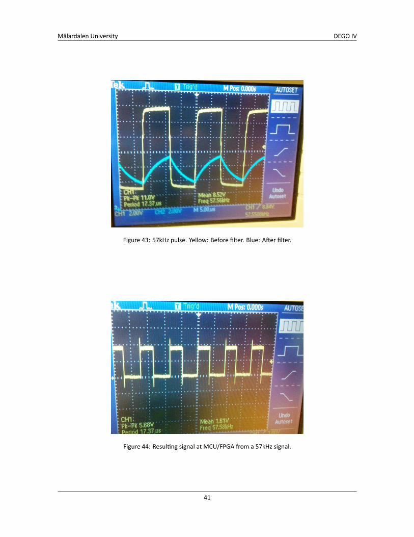
Results:The physical result supports the simulated one. The lower frequencies passes quite unaffected [Figure 41],while the higher frequencies showmore of a dampening effect [Figure 42, 43]. The final result a er atMCU/F-PGA show a good and noise free signal [Figure 44].
Figure 41: 5kHz pulse. Yellow: Before filter. Blue: A er filter.
Figure 42: 20kHz pulse. Yellow: Before filter. Blue: A er filter.
40
Mälardalen University DEGO IV
Figure 43: 57kHz pulse. Yellow: Before filter. Blue: A er filter.
Figure 44: Resul ng signal at MCU/FPGA from a 57kHz signal.
41
Mälardalen University DEGO IV
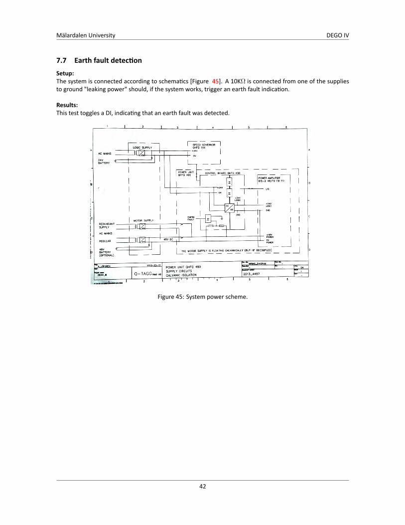
7.7 Earth fault detec onSetup:The system is connected according to schema cs [Figure 45]. A 10KΩ is connected from one of the suppliesto ground "leaking power" should, if the system works, trigger an earth fault indica on.
Results:This test toggles a DI, indica ng that an earth fault was detected.
Figure 45: System power scheme.
42

Mälardalen University DEGO IV
7.8 CANSetup:One node is connected to an electrical motor with a built in power amplifier. Messages are sent to rotate themotor. The messages are also read by a monitoring device.
Results:CAN messages were received as expected. The slew rate of the transceiver was at first programmed to thefastest possible se ng which resulted in 1W use of power hea ng up the transceiver to 50 C in an ambienttemperature of 22 C. The se ngs were changed and the effect was lowered to approximately 0.5W.
43
Mälardalen University DEGO IV
8 Results• Safety cri cal aspects
As much system func onality as possible is integrated into the FPGA to lower the number of discretecomponents. From a safety standpoint this may not always be the best solu on. Inves ga on of failedsystems show thermo stress as a primary cause to system failures and therefore layout factors havebeen considered for lower opera ng temperature. Actuator control is separated from the rest of thesystem with a fed of power galvanically isolated. Another Fault-containment region is made by galvanicisola on at the FPGA. For safer opera ons it might be suitable to implement a TripleModular RedundantArchitecture in the FPGA to ensure correct processing. For safer bus opera ons it might be useful toimplement a RS-485 protocol opera ng on two duplicated transmission lines, similar as to what SAFEbusdoes. Voltage monitoring has been implemented and all system nodes are isolated in self-containmentregions by galvanic isola on.
• Decoupling modelCrea ng a simplified model for determining and op mizing the decoupling was theorized. To ensure sta-ble func ons of the FPGA a decoupling of the IC is used. Basically it all comes down to manipula ng thesystem impedance to control the voltage ripple. There will be a maximum allowed impedance to get adesired voltage ripple. The problema c nature of the decoupling is the parasi c proper es of the PCBand package, these will induce a change in the impedance over a frequency range.
A major factor counterac ng the decoupling capacitors is the induc ve parasi cs. The capacitors haveminimum impedance at it's resonance frequency as well as the induc ve parasi cs have it's highestimpedance at its resonance frequency. The idea was to match these resonance frequencies to fla enthe impedance curve. The resonance frequency should be placed higher than the ripple frequency.
The best results of the decupling are acquired when good layout methods are in use. Matching the res-onance frequencies of decoupling and the induc ve parasi cs was a method that gave no considerableeffects.
• Auto-calibra onAc ve auto-calibra on could be done with components like digital poten ometers. Auto-calibra onshapes a formidable challenge. A good course of ac on is to avoid all ac ve auto-calibra on if possi-ble, it is more efficient using a solu on with precision components or a passive calibra on by a discretedesign. E.g. A feedback signal biasing a transistor for regula ng the current independent from the load,temperature and other external factors.
• ProgrammableThere are several possible solu ons to this problem, using a FPGA simplifies the method considerably.While having programmable logic it also offers many I/O opening up an effec ve and low cost methodof opera ng digital switches by transistors as long as polarity and voltage levels allow the solu on towork. If alterna ng current is needed a switch made by a solid state relay could be implemented. Theprogrammable nature is set by a VHDL layer separated from the so ware.
• Analog outputCrea ng an analog output with stable current showed to be a real challenge. Despite many differentapproaches to digitalize the output, a simple and cost effec ve solu on could not be found. The bestsolu ons were all based on a closed feedback loop adjus ng an amplifica on stage. The func onality ofthe feedback loop was never verified. finally a analog solu on by biasing a transistor was implemented.
• Measurement of iner aImplementa on of gyroscopes were selected as the be er solu on for measuring rota on of the PCBcompared to accelerometers.
44
Mälardalen University DEGO IV
• Digital inA need for durable DI was needed. The DI should be able to withstand very large transients. It waspreferable if the new DI had a faster step response. A new design was implemented that had a very highresistance on its input and a be er filtering. With a be er filter the idea was to limit the ringing givinga faster step response. Simula ons showed a high dampening of the signal and a certain delay. Tes ngshowed be er filtering and a somewhat improved step response.
• Product life & maintenanceSupply voltages are very stable and there is very li le overshoot on the inputs. The design of the circuitboard such as layout will affect the PCB endurance and life me. Tes ng indicates the life me to be morethan ten years14. There is li le data to support accurate es mates a er the ten years period and for nowthe life me of the product is considered to be 10 years.
14Altera, "Cyclone IV Device Handbook"http://www.altera.com/literature/hb/cyclone-iv/cyclone4-handbook.pdf
45
Mälardalen University DEGO IV
9 DiscussionThe verified results are as expected for signal condi oning. Unfortunately there were issues with the PCB,stopping the moun ng of the FPGA package in assembly. Therefore there was no HDL tested on this system.An MCU was patched on to the PCB to process signals and relay results. The prototype shows that the systemdesign works and that necessary func ons can be delivered.
Parts of the design are in need of improvements. Some areas require more of a finishing touch and otherareas need a second look at available op ons on the market. Looking at the complexity of the PCB, one couldask: is an FPGA suitable for safety cri cal system? Do the gain outweigh the cost of implementa on?There are several different angles to consider, such as package (some claim BGA to be fragile and others claimit to be the most robust op on on the market), cost, life- me and much more. A possible approach might beto migrate to an Advanced Reduced instruc on set computer Machine (ARM). Using an ARM equipped withfloa ng point unit and higher clock-frequency, there will be a sufficient speed upgrade to this system for han-dling calcula on and signal condi oning.
An interes ng aspect giving the FPGA solu on more credibility would be a new genera on FPGA containingboth a hard-core and a so -core. Using such a device opens up a new op on of running par al reconfigura-on, moving the flexibility of the system to a new level. The selected components were in general ample and
suitable. Most components selected will be used in the upcoming second prototype. One of themain concernsfor the new prototype is the rou ng. The auto-router used has despite great efforts not delivered acceptableresults. The rou ng has to be done manually to get be er results and to fulfill the requirements of IPC-2221.Further tes ng of the current prototype is needed to answer some of the ques ons that s ll exist and rendera new design.
46
Mälardalen University DEGO IV
10 Future workThe electronics pla orm requires further development but there are also future changes to be made in so -ware. The so ware focuses on system integra on.
10.1 Electronics• Programing interface
FPGA image loading from a simple flash memory could replace the need for the serial configura ondevice.
• ARMEvalua ng and implemen ng a change from FPGA to an ARM MCU with the benefit of lowering thenumber of complex design elements and cost.
• TransistorsSome of the transistors are all to largely dimensioned for their intended func on. A overhaul of thesystem could make be er use of components and system resources.
• Voltage regulatorsThe 12V DC-DC converter could be replaced by a 5V DC-DC converter thus removing the 5V regulator.Alterna vely using a DC-DC converter with less transforma on ra o to lower DC-DC price. The analogpower to the FPGA (2.5V) could be replaced with a voltage stabilized by a zener-diode due to low currentconsump on.
• BluetoothA flexible approach to interfacing user controls and sensors is to use wireless technology. Industry stan-dard Bluetooth is a good op on. The transceiver for such a wireless system may be integrated in differ-ent loca ons. Determining the need for Bluetooth communica on and in which system to integrate thetransceivers is an interes ng future project.
10.2 System integra on• Touchscreen
A future improvement of the system is to integrate an embedded touchscreen where an applica onservermay run. TheAID so waremight bedeveloped to run in the emmbeded systemor in an applica onserver, these ques ons are evaluated in two separate thesis work.
• Intellectual PropertyThe Intellectual Property component layer is lacking watchdog, Ethernet, CAN and I2C controllers. Thisis the founda on for an upcoming thesis if a FPGA approach is to be con nued.
• SPIDER BusFor the future it might be useful to implement an op cal SPIDER bus free of all electromagne cal inter-ference.
10.3 Further tes ngThere is a need for a system test simula ng a twin engine setup. To ensure a successful cer fica on processthere are some environmental tes ng to be preformed. E.g. thermo-stress, radiated immunity, radiated emis-sion, and there should be no indica on of radiated or conducted emissions.
47
Mälardalen University DEGO IV
10.3.1 Field tes ng
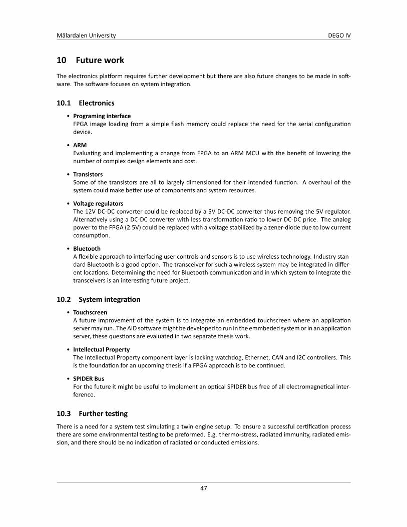
A er a successful system test, there will be a field test on a Bal c sea RoPax or cruise ship where real-lifecondi ons are tested [Figure 46 - 49]. The DEGO IV will replace one of their four exis ng governors in a longterm test of two months. If a system failure would occur there is a redundancy in the other three engines.The ship would reach its intended port without delay on one of the twin engine setups. Tes ng as crash-stops,over-speed, maneuverability tes ng is only allowed in open sea. The tes ng is done on the Cinderella or asimilar sized ship (Figure [46] - [49]).
10.3.2 Cer fica on
A er the field tes ng the system will be sent to an independent cer fica on agency for external revision andtes ng.
Figure 46: Viking Line cruise ship intended for tes ng.
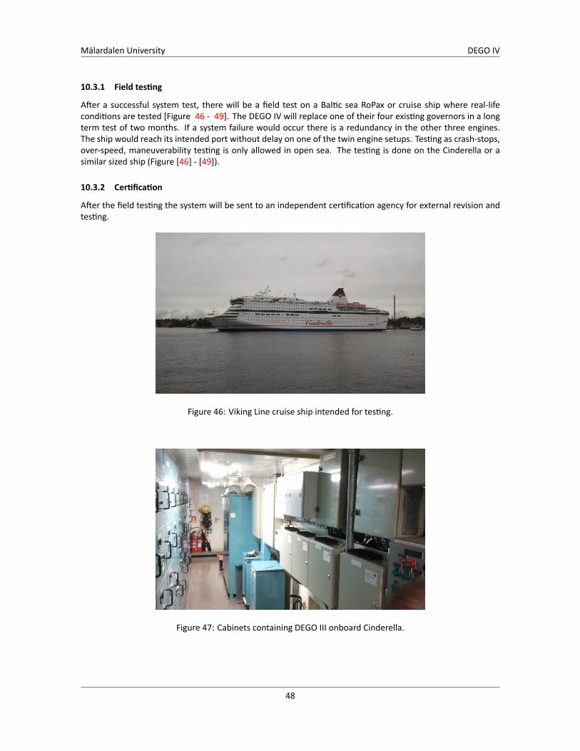
Figure 47: Cabinets containing DEGO III onboard Cinderella.
48
Mälardalen University DEGO IV
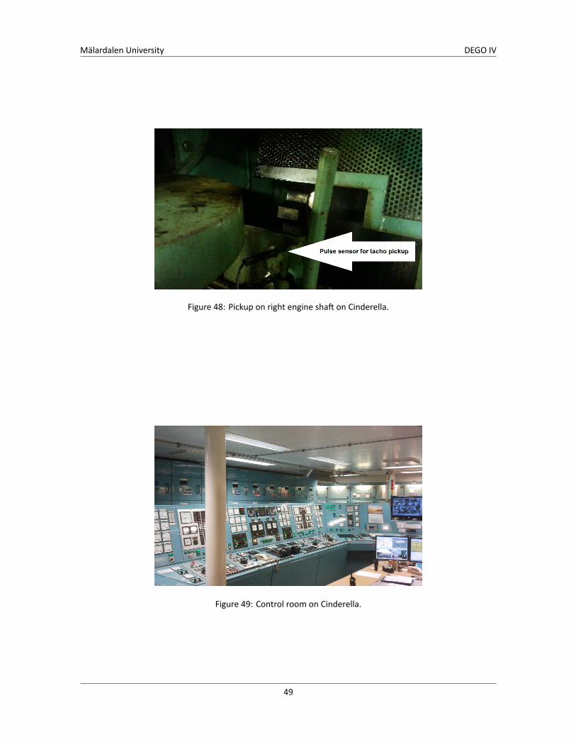
Figure 48: Pickup on right engine sha on Cinderella.
Figure 49: Control room on Cinderella.
49
Mälardalen University DEGO IV
References[1] Altera. Pdn design methodology. http://www.altera.com/literature/an/an574.pdf, 2009. [On-
line; accessed 12-December-2012].
[2] K. Badzmirowski and B. Jackiewicz. Effec veness of various dithering architectures for linearisa on ofhigh-resolu on oversampling a/d converters. In Advanced A/D and D/A Conversion Techniques and TheirApplica ons, 1999. Third Interna onal Conference on (Conf. Publ. No. 466), pages 175 --178, 1999.
[3] M. Baleani, A. Ferrari, L. Mangeruca, A. Sangiovanni-Vincentelli, Maurizio Peri, and Saverio Pezzini. Fault-tolerant pla orms for automo ve safety-cri cal applica ons. In Proceedings of the 2003 interna onalconference on Compilers, architecture and synthesis for embedded systems, CASES '03, pages 170--177,New York, NY, USA, 2003. ACM.
[4] E. Bohl, Th. Lindenkreuz, and R. Stephan. The fail-stop controller ae11. In Test Conference, 1997. Proceed-ings., Interna onal, pages 567 --577, nov 1997.
[5] J. Burden, P.A. Curry, D. Roby, and F. Love. Introduc on to the next genera on automa c test system(ngats). In Autotestcon, 2005. IEEE, pages 16 -- 19, sept. 2005.
[6] P.L. Cheng, S.Y.Y. Leung, T.W. Law, C.K. Liu, J.I.T. Chong, and D.C.C. Lam. Quan ta ve analysis of resis-tance tolerance of polymer thick film printed resistors. Components and Packaging Technologies, IEEETransac ons on, 30(2):269 --274, june 2007.
[7] Maria Lindén. Christer Gerdtman, Ylva Bäcklund (former). A gyro sensor based computer mouse with ausb interface: A technical aid for motor-disabled people. 2012.
[8] T. Giuma and A. Ebenal. Programmable hardware and the new analog capacity. In Systems, 2007. ICONS'07. Second Interna onal Conference on, page 19, april 2007.
[9] Jack W Judy. Microelectromechanical systems (mems): fabrica on, design and applica ons. Smart Ma-terials and Structures, 10(6):1115, 2001.
[10] Fangjuan Qi and Jim Liu. Research on failure modes of bga assemblies with lead-free solder on differ-ent pcb materials. In Electronic Packaging Technology Proceedings, 2003. ICEPT 2003. Fi h Interna onalConference on, pages 396 --400, oct. 2003.
[11] John Rushby. A comparison of bus architectures for safety-cri cal embedded systems. pages 306--323.Springer-Verlag, 2001.
[12] Alfred R. Schuler, Anthony Gramma kos, and Kenneth A. Fegley. Measuring rota onal mo on with linearaccelerometers. Aerospace and Electronic Systems, IEEE Transac ons on, AES-3(3):465 --472, may 1967.
[13] Dave S. Steinberg. Preven ng Thermal Cycling and Vibra on Failures in Electronic Equipment. JohnWiley& sons, New York, USA, 2001.
[14] Vishay. Basics of linear fixed resistors. http://www.element14.com/community/docs/DOC-22086,2008. [Online; accessed 28-august-2012].
[15] Heinz Zenker, Alexander Gerfer, and Bernhard Rall. Triology of Inductors. Swiridoff Verlag., Künzelsau,GERMANY, 2005.
[16] Li Zhiming, Jiao San, and Xu Guozhi. Automa c hardware test system for complex digital systems. InCommunica ons, Circuits and Systems and West Sino Exposi ons, IEEE 2002 Interna onal Conference on,volume 2, pages 1351 -- 1355 vol.2, june-1 july 2002.
50
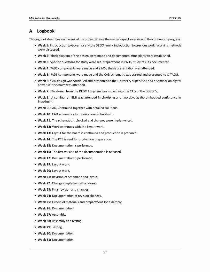
Mälardalen University DEGO IV
A LogbookThis logbook describes eachweek of the project to give the reader a quick overview of the con nuous progress.
• Week1: Introduc on toGovernor and theDEGO family, introduc on to previouswork. Workingmethodswere discussed.
• Week 2: Block diagram of the design were made and documented, me plans were established.
• Week 3: Specific ques ons for study were set, prepara ons in PADS, study results documented.
• Week 4: PADS components were made and a MSc thesis presenta on was a ended.
• Week 5: PADS components were made and the CAD schema c was started and presented to Q-TAGG.
• Week 6: CAD design was con nued and presented to the University supervisor, and a seminar on digitalpower in Stockholm was a ended.
• Week 7: The design from the DEGO III system was moved into the CAD of the DEGO IV.
• Week 8: A seminar on EMI was a ended in Linköping and two days at the embedded conference inStockholm.
• Week 9: CAD, Con nued together with detailed solu ons.
• Week 10: CAD schema cs for revision one is finished.
• Week 11: The schema c is checked and changes were implemented.
• Week 12: Work con nues with the layout work.
• Week 13: Layout for the board is con nued and produc on is prepared.
• Week 14: The PCB is sent for produc on prepara on.
• Week 15: Documenta on is performed.
• Week 16: The first version of the documenta on is released.
• Week 17: Documenta on is performed.
• Week 19: Layout work.
• Week 20: Layout work.
• Week 21: Revision of schema c and layout.
• Week 22: Changes implemented on design.
• Week 23: Final revision and changes.
• Week 24: Documenta on of revision changes.
• Week 25: Orders of materials and prepara ons for assembly.
• Week 26: Documenta on.
• Week 27: Assembly.
• Week 28: Assembly and tes ng.
• Week 29: Tes ng.
• Week 30: Documenta on.
• Week 31: Documenta on.
51
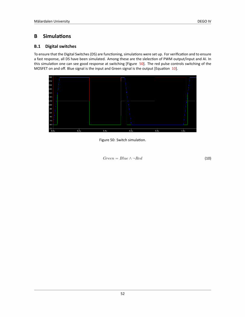
Mälardalen University DEGO IV
B Simula ons
B.1 Digital switchesTo ensure that the Digital Switches (DS) are func oning, simula ons were set up. For verifica on and to ensurea fast response, all DS have been simulated. Among these are the slelec on of PWM output/input and AI. Inthis simula on one can see good response at switching [Figure 50]. The red pulse controls switching of theMOSFET on and off. Blue signal is the input and Green signal is the output [Equa on 10].
Figure 50: Switch simula on.
Green = Blue ∧ ¬Red (10)
52
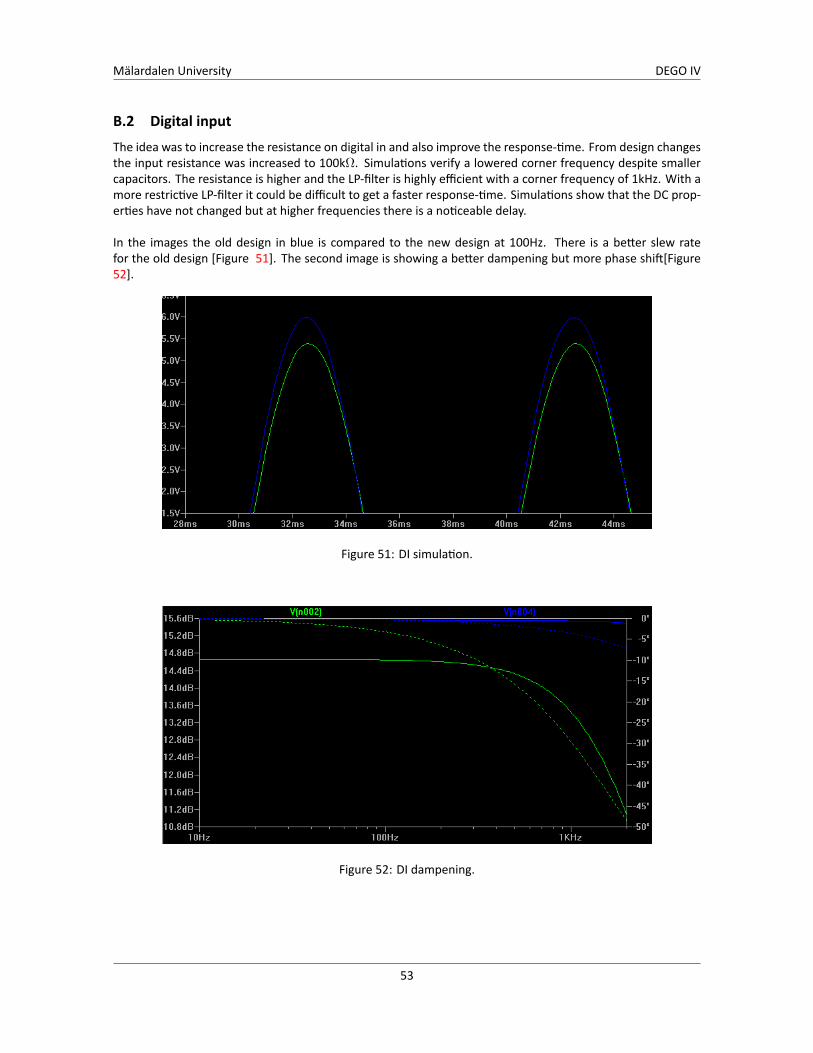
Mälardalen University DEGO IV
B.2 Digital inputThe idea was to increase the resistance on digital in and also improve the response- me. From design changesthe input resistance was increased to 100kΩ. Simula ons verify a lowered corner frequency despite smallercapacitors. The resistance is higher and the LP-filter is highly efficient with a corner frequency of 1kHz. With amore restric ve LP-filter it could be difficult to get a faster response- me. Simula ons show that the DC prop-er es have not changed but at higher frequencies there is a no ceable delay.
In the images the old design in blue is compared to the new design at 100Hz. There is a be er slew ratefor the old design [Figure 51]. The second image is showing a be er dampening but more phase shi [Figure52].
Figure 51: DI simula on.
Figure 52: DI dampening.
53
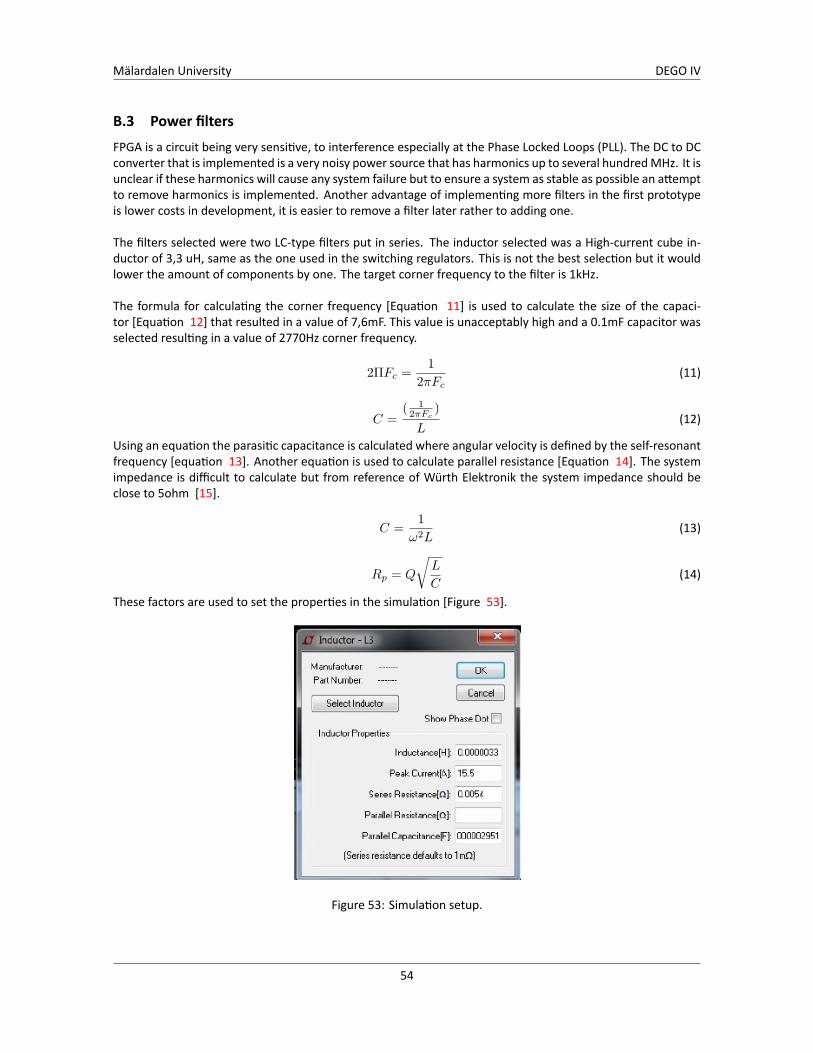
Mälardalen University DEGO IV
B.3 Power filtersFPGA is a circuit being very sensi ve, to interference especially at the Phase Locked Loops (PLL). The DC to DCconverter that is implemented is a very noisy power source that has harmonics up to several hundredMHz. It isunclear if these harmonics will cause any system failure but to ensure a system as stable as possible an a emptto remove harmonics is implemented. Another advantage of implemen ng more filters in the first prototypeis lower costs in development, it is easier to remove a filter later rather to adding one.
The filters selected were two LC-type filters put in series. The inductor selected was a High-current cube in-ductor of 3,3 uH, same as the one used in the switching regulators. This is not the best selec on but it wouldlower the amount of components by one. The target corner frequency to the filter is 1kHz.
The formula for calcula ng the corner frequency [Equa on 11] is used to calculate the size of the capaci-tor [Equa on 12] that resulted in a value of 7,6mF. This value is unacceptably high and a 0.1mF capacitor wasselected resul ng in a value of 2770Hz corner frequency.
2ΠFc =1
2πFc(11)
C =( 12πFc
)
L(12)
Using an equa on the parasi c capacitance is calculated where angular velocity is defined by the self-resonantfrequency [equa on 13]. Another equa on is used to calculate parallel resistance [Equa on 14]. The systemimpedance is difficult to calculate but from reference of Würth Elektronik the system impedance should beclose to 5ohm [15].
C =1
ω2L(13)
Rp = Q
√L
C(14)
These factors are used to set the proper es in the simula on [Figure 53].
Figure 53: Simula on setup.
54

Mälardalen University DEGO IV
First part was to design the filter for the highest frequencies. There will be an amplifica on just beforethe filter starts dampening the harmonics [Figure 54]. To eliminate the amplifica on of the signal the seriesresistance is increased to a reasonable value [Figure 55].
Figure 54: High frequency LC-filter.
Figure 55: High frequency LC-filter.
55
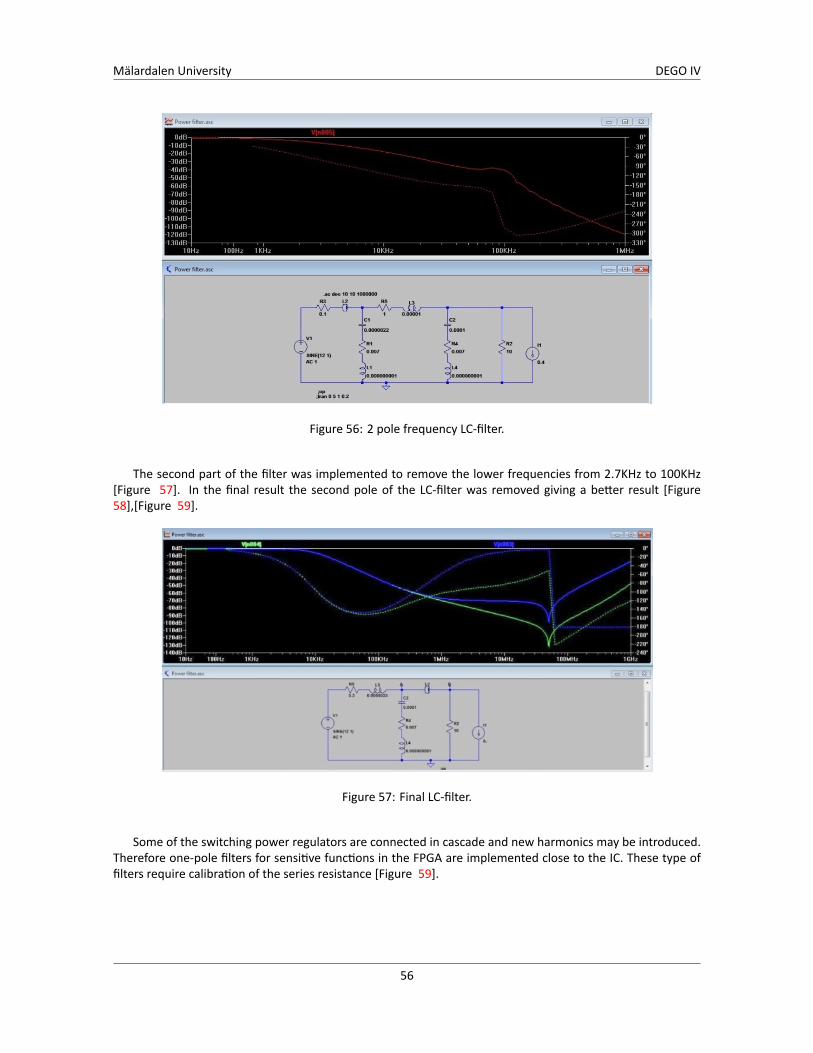
Mälardalen University DEGO IV
Figure 56: 2 pole frequency LC-filter.
The second part of the filter was implemented to remove the lower frequencies from 2.7KHz to 100KHz[Figure 57]. In the final result the second pole of the LC-filter was removed giving a be er result [Figure58],[Figure 59].
Figure 57: Final LC-filter.
Some of the switching power regulators are connected in cascade and new harmonics may be introduced.Therefore one-pole filters for sensi ve func ons in the FPGA are implemented close to the IC. These type offilters require calibra on of the series resistance [Figure 59].
56

Mälardalen University DEGO IV
Figure 58: Final LC-filter.
Figure 59: Final one pole LC-filter, with decoupling capacitors.
57
Mälardalen University DEGO IV
C Thesis Specifica on
We reserve all rights in this document and in the information contained therein. Reproduction, use or disclosure to third parties without express authority is strictly forbidden.
Q-TAGG R&D AB
Prep. George Fodor 2012-09-01 MSc Thesis No of sh. Appr. Arne Löfgren Governors Electronics for Diesel Resp. dept. Engines Document number Lang. Rev. Sheet
Q-TAGG R&D AB Q12-020.doc en 1 1
Technical Document 6TDAP1.DOT
1. Abstract
Title: Governor Electronics for Diesel Engines
Project: MSc Project, 30 points, Mälardalen University College, Västerås, Sweden
Company: QTAGG R&D AB, Västerås, Sweden
Project Start: August 2012
Contacts: Tomas Lindqvist, +46 70-534 77 00; [email protected]
George Fodor, +46 72-350 74 12; [email protected]
2. Background
A governor is an electronic equipment used to control the speed of diesel engines of a ship. Diesel engines are used on ships for propulsion and for generation of electrical power. Governors are safety critical systems since loss of propulsion or of electrical power could have serious consequences for the safety of a ship.
In many cases ships have several diesel engines and a variety of generation and propulsion configurations. Thus governors communicate among them and also with other control systems on ship to coordinate start and stop of diesel engines and the amount of power generated by the engines. Moreover governors are reading signals from sensors and are sending commands to actuators and to electrical power breakers.
Governors can be used on commercial ships only after approval from marine classification societies.
The MSc thesis work should ensure that all interfaces and communication requirements are satisfied both functionally and from a safety-critical point of view.
3. Project description
The governor will be designed as a single electronic board. The board design is based on a FPGA chip. The scope of the thesis is to design the electronics around the FPGA chip; the FPGA coding and application software is not within the scope of the project. All necessary pin functions of the FPGA are available and described in a document.
All signals to and from the FPGA are pulses or serial communication protocols (I2C, SPI). Analog inputs and outputs are also implemented as PWM signals. All process signals must be isolated and protected against overvoltage. The board should be able to successfully pass radio interference tests and marine classification societies tests.
58

We reserve all rights in this document and in the information contained therein. Reproduction, use or disclosure to third parties without express authority is strictly forbidden.
Q-TAGG R&D AB
Q12 Document number Lang. Rev. Sheet
Q-TAGG R&D AB Q12-020.doc en 1 2 Technical Document 6TDAP1.DOT
4. Specifications:
1. Analog inputs: 8 lines, 0-10V / 0-20 mA (selectable), 14 bits precision, isolated, filter, overvoltage protection
2. Analog outputs: 5 lines, 12 bits precision,+/- 10VDC, 0-20mA (selectable), isolated, 10 KHz PWM
3. Digital Inputs, 24V, 24 lines, isolated, overvoltage protection
4. Digital Outputs, 24V, 8 lines, isolated, max 100mA (2.4W)
5. Display interface, perhaps touch screen (type to be decided)
6. Flash memory interface (type and size to be decided)
7. USB interface
8. TCP/IP interface, 1 port
9. RS232/RS485 interface, 2 ports
10. Pulse inputs, 24V, 0-5000 Hz range, 4 lines, isolated, overvoltage protection
11. Bluetooth interface (to be decided together with the display interface)
12. LED lamps or other method that makes visible the set-up of the board, for example if pulses are arriving, if the analog signals are set for the 0…10V range or for the 0-20mA range, etc.
13. All components to be surface mounted.
14. Temperature, supply current and ground monitoring of the board
5. Research questions of the thesis
There are many research questions related to the design. Most relevant are the following:
1. A solution that complies with, or is better than the requirements of the Marine Classification Societies
2. A solution for the electronics with no switches, jumpers or other components that need manual operations on the board. In other words, an operator should never need to open the cover of the board.
3. The design needs a solution for electronics that does not need any manual calibration.
4. The board should have a self-test function or alternatively an easy-to-test function. The idea is to have a green LED which, when lit, indicates that the whole board with all components is correct. The goal for this function is to have a fast and secure production.
5. A solution to have a 3D angle sensor on the electronics board, filter in three directions, calibration of zero position

We reserve all rights in this document and in the information contained therein. Reproduction, use or disclosure to third parties without express authority is strictly forbidden.
Q-TAGG R&D AB
Q12 Document number Lang. Rev. Sheet
Q-TAGG R&D AB Q12-020.doc en 1 3 Technical Document 6TDAP1.DOT
6. Voltage control solution. Evaluate current solution and propose modern components (switched power supplies)
7. Power failure detection for the voltage supplies on the board (24V, +/-15V, 2.5V)
8. Temperature monitoring method (use FPGA sensor or external sensor) and methods to reset a high current
9. A method to have visible unit ID and each board to have own ID. Do we need up/down buttons to setup the ID? Touch screen?
10. A method to have +/-20mA analog output. That would need an OA but the OA has not enough current. Find a solution that can supply bipolar current
11. No calibration of the current output for AO
12. Switch by software between current / voltage inputs and outputs
13. To have an electronic selection for the type of tacho: PNP or NPN
14. To have the break logic / manual for the actuator according to specification
15. Inverted PWM signal (TB7 pp 7) by software
16. Do we need calibration for actuator current measuring?
17. Software selection to bypass or not the voltage controller (A1P24 jumper)
18. The July number of the Electronics Design magazine has a list of 2012 Year’s Top Components. Which of these components are suitable for the design of the governor?
6. Project output
1. Documentation (thesis) for the electronics solution
2. Prototype board, tested
3. EMC, vibration, heat and electronics-part for marine classification tests
7. Project support from QTAGG R&D side
- QTAGG supplies computers and software for the design of the electronics
- All specification details, solutions for the existing version of the governor are available from QTAGG
- Previous tests with Classification Societies are available
- Experimental board with an existing solution are available
- The work is done at QTAGG location
- Specification with the FPGA interface and pin description available

We reserve all rights in this document and in the information contained therein. Reproduction, use or disclosure to third parties without express authority is strictly forbidden.
Q-TAGG R&D AB
Q12 Document number Lang. Rev. Sheet
Q-TAGG R&D AB Q12-020.doc en 1 4 Technical Document 6TDAP1.DOT
- A planning of the project will be done together with the student and with the University supervisor
8. Project support from University side
- The University names a project supervisor to be involved in the research questions
- The supervisor should be in the field required for this project: electronics design
- The student may use the University library for literature studies
We reserve all rights in this document and in the information contained therein. Reproduction, use or disclosure to third parties without express authority is strictly forbidden.
Q-TAGG R&D AB
Q12 Document number Lang. Rev. Sheet
Q-TAGG R&D AB Q12-020.doc en 1 5 Technical Document 6TDAP1.DOT
REVISION
Rev. Page (P) Chapt.(C)
Description Date Dept./Init.
- - First release SD/GF 1 Added project outputs and more research questions 2012/08/08/
SD/GF

Mälardalen University DEGO IV
D Circuit diagramCircuit diagrams are classified. Ques ons rela ng to electronics can be asked by mail. No detailed solu onsare revealed.
63
Mälardalen University DEGO IV
E DEGOIII Manual
ABB Marine Rotterdam
Title : User’s Manual Document no.: 3BNM005401D109 Sheet : 1(9)
Name : DEGO III, Governor unit Rev : D
Subject : Technical Data Date : 02-03-29
9. TECHNICAL DATA ...................................................................................................... 3
9.1 GENERAL ................................................................................................................... 3 9.1.1 Environmental Conditions all units. .................................................................. 3 9.1.2 Dimensions And Weight QHFQ 100 series ....................................................... 3 9.1.3 Dimensions And Weight QHFQ 552 series ....................................................... 3 9.1.4 Types And Article Numbers ............................................................................... 4 9.1.5 Class approvals ................................................................................................. 4
9.2 CONTROL FUNCTIONS ................................................................................................ 5 9.2.1 Power Supply For The Control Circuits ........................................................... 5 9.2.2 Accuracy ............................................................................................................ 5 9.2.3 Pulse Inputs (Speed Signal Inputs) .................................................................... 5 9.2.4 Speed Pick-up Supply ........................................................................................ 6 9.2.5 Analog Inputs .................................................................................................... 6 9.2.6 Digital Inputs .................................................................................................... 6 9.2.7 Analog Outputs ................................................................................................. 6 9.2.8 Digital Outputs .................................................................................................. 7 9.2.9 Alarm Outputs ................................................................................................... 7 9.2.10 Bus Communication .......................................................................................... 7 9.2.11 Microprocessor ................................................................................................. 7 9.2.12 Memory Arrangement ....................................................................................... 7 9.2.13 Control Algorithms ............................................................................................ 8 9.2.14 Internal Supervision .......................................................................................... 8 9.2.15 Display Unit ...................................................................................................... 8
9.3 POWER AMPLIFIER FOR ASAC CONTROL. .................................................................. 9 9.3.1 Power Supply for ASAC 70 ............................................................................... 9 9.3.2 Power Supply for ASAC 200/400 ...................................................................... 9 9.3.3 Actuator Drive 0utput Current .......................................................................... 9 9.3.4 Manual Control ................................................................................................. 9 9.3.5 Earth Fault Detection ....................................................................................... 9 9.3.6 Current Measurement ....................................................................................... 9
64
ABB Marine Rotterdam
Title : User’s Manual Document no.: 3BNM005401D109 Sheet : 2(9)
Name : DEGO III, Governor unit Rev : D
Subject : Technical Data Date : 02-03-29
Approvals: Prepared: Arne Löfgren
Checked: Harry Jezuit
Approved: Fred van den Hoonaard
Revision History:
Rev: Date: Reason: Par:
1 9932 New header HJ
2 9934 IP class HJ
B 9948 Cub dimensions, added txt solid state relay. HJ
C 00-02-14 Formatting of chapter HJ
D 02-03-29 QHFQ 552 implemented HJ
ABB Marine Rotterdam
Title : User’s Manual Document no.: 3BNM005401D109 Sheet : 3(9)
Name : DEGO III, Governor unit Rev : D
Subject : Technical Data Date : 02-03-29
9. Technical Data
9.1 General
9.1.1 Environmental Conditions all units.
Protection: Without cooling fan IP 54 With cooling fan IP 20
Max. ambient temperature: 0-55C
Max. amb. temp. with cooling fan installed: 0-70C Max. humidity: Rh 98% non condensing Max. allowed vibration: According to the class rules EMC status: According to class rules and IEC EN 61000-2, -3, -4, -5,6 and EN 55011
9.1.2 Dimensions And Weight QHFQ 100 series
Width: 400 mm Height including mounting flanges: 465 mm Depth: 170 mm Mounting bolts: M8 Mounting hole pattern: W: 350 mm, H:430 mm Cable connections: 4xPr28(Pg21), 8xPr22.5(Pg16) Weight: 15 kg Mounting dimension picture See Chapter 3.3
9.1.3 Dimensions And Weight QHFQ 552 series
Width: 450 mm Height including mounting flanges: 760 mm Depth: 160 mm Mounting bolts: M8 Mounting hole pattern: W: 400 mm, H:730 mm Cable connections: 12xPr28(Pg21), 12xPr22.5(Pg16) Weight: 25 kg Mounting dimension picture See Chapter 3.4
ABB Marine Rotterdam
Title : User’s Manual Document no.: 3BNM005401D109 Sheet : 4(9)
Name : DEGO III, Governor unit Rev : D
Subject : Technical Data Date : 02-03-29
9.1.4 Types And Article Numbers
Type Article Number Configuration
QHFQ 110 3BNM 005401R0 No drive installed QHFQ 111 3BNM 005401R1 One 80V amplifier fitted QHFQ 112 3BNM 005401R2 Two 80V amplifiers fitted QHFQ 113 3BNM 005401R3 One 190V amplifier fitted QHFQ 114 3BNM 005401R4 Two 190V amplifier fitted QHFQ 115 3BNM 005401R5 One 80V and one 190V amplifier fitted QHFQ 550 3BNM 005402R0 No drive installed QHFQ 551 3BNM 005402R1 Tw0 80V amplifier fitted QHFQ 552 3BNM 005402R2 One 80V amplifiers fitted QHFQ 553 3BNM 005402R3 One 190V amplifier fitted QHFQ 554 3BNM 005402R4 Two 190V amplifier fitted QHFQ 555 3BNM 005402R5 One 80V and one 190V amplifier fitted QHFQ 270 3BNM 005411R1 Fan Unit Note: 80Volt amplifier is used for ASAC 70 application Note: 190 Volt amplifier is used for ASAC 200 / 400 applications. For spares and accessories, see listing in chapter Accessoires and Spare parts.
9.1.5 Class approvals
Approvals from: American Bureau of Shipping Bureau Veritas Det Norske Veritas Germanishe Lloyd Lloyds Register of Shipping Registro Italiano Navale
ABB Marine Rotterdam
Title : User’s Manual Document no.: 3BNM005401D109 Sheet : 5(9)
Name : DEGO III, Governor unit Rev : D
Subject : Technical Data Date : 02-03-29
9.2 Control Functions
9.2.1 Power Supply For The Control Circuits
External Voltage: 18-32VDC. Protected against reversed
polarity. The supply is floating referred to ground.
Current: 0.4A (electronics only) Additional 0.5A(1.0A) for brake on 1 or 2 actuator(s) Additional 0.4A for cooling fan Additional 0.5A for additional sensors etc.
Recommended supply fuse: 2A (1 actuator) 4A (2 actuators)
Internal Voltages +5V, +15V, -15V, 24V floating against ground
+5V for microprocessor and communication ports(minus pole grounded)
Supervision Provided for +5,+15 and -15V
9.2.2 Accuracy
Speed control: +/- 0.5% Limits: +/- 1% Load sharing: +/- 1% RPM measurement rounding error: Max. 0.6%
9.2.3 Pulse Inputs (Speed Signal Inputs)
4 channels with the following data: LED indication for each channel Both PNP and NPN pickups can be used, even mixed Frequency division by /1, /2, 4, /8, and /16 for each channel by means of jumpers.
Each pick-up can have its own frequency range) Input impedance 3k Voltage for logical "0" state <4V Voltage for logical "1" state >9V Frequency range 0-250/500/1000/ 2000/4000 Hz Max. number of teeth on the flywheel when the RPM filter is used: 150/300/450/ 600/750 Max. time interval(min. frequency) that can be measured between pickup pulses: 33 sec(0.03Hz) Min. time interval(max. frequency) that can be measured between pick up pulses: 0.2 ms (PNP pickups) 0.05 ms (NPN pickups)
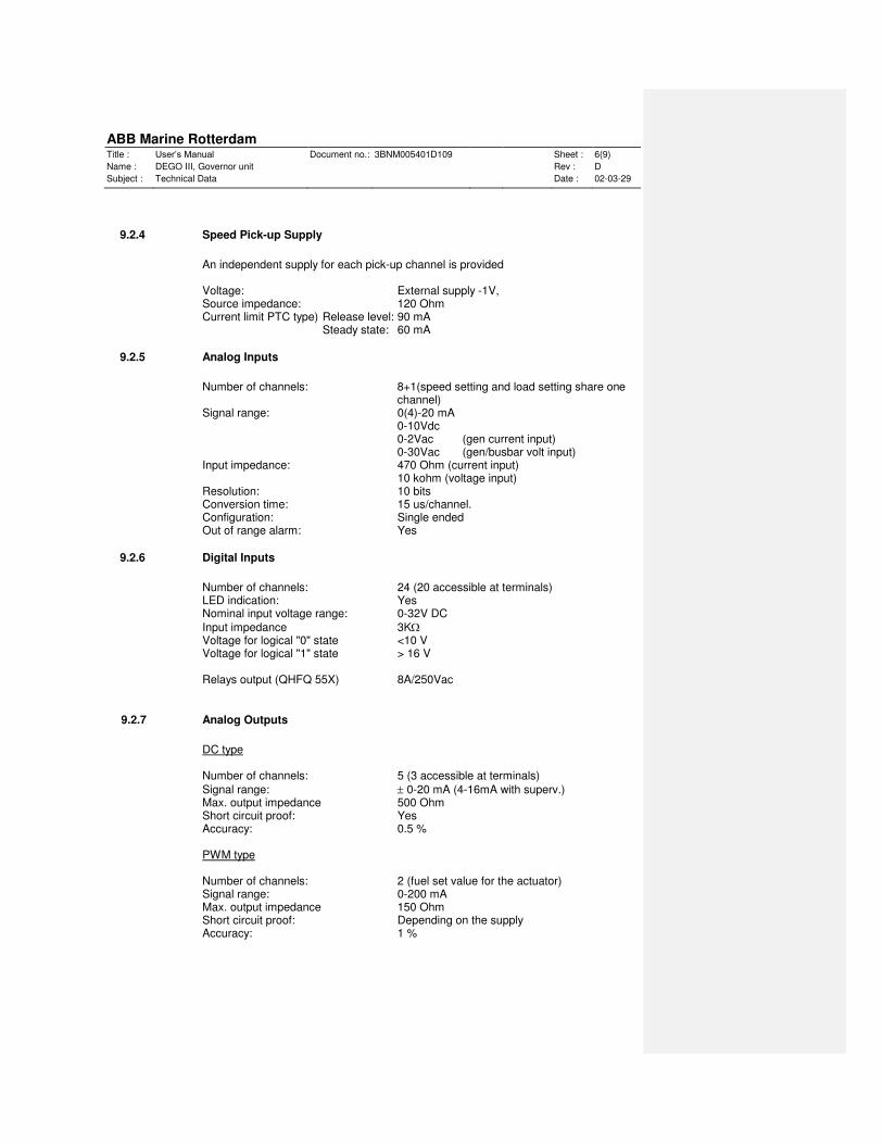
ABB Marine Rotterdam
Title : User’s Manual Document no.: 3BNM005401D109 Sheet : 6(9)
Name : DEGO III, Governor unit Rev : D
Subject : Technical Data Date : 02-03-29
9.2.4 Speed Pick-up Supply
An independent supply for each pick-up channel is provided Voltage: External supply -1V, Source impedance: 120 Ohm Current limit PTC type) Release level: 90 mA Steady state: 60 mA
9.2.5 Analog Inputs
Number of channels: 8+1(speed setting and load setting share one
channel) Signal range: 0(4)-20 mA
0-10Vdc 0-2Vac (gen current input) 0-30Vac (gen/busbar volt input)
Input impedance: 470 Ohm (current input) 10 kohm (voltage input) Resolution: 10 bits Conversion time: 15 us/channel. Configuration: Single ended Out of range alarm: Yes
9.2.6 Digital Inputs
Number of channels: 24 (20 accessible at terminals) LED indication: Yes Nominal input voltage range: 0-32V DC
Input impedance 3K Voltage for logical "0" state <10 V Voltage for logical "1" state > 16 V Relays output (QHFQ 55X) 8A/250Vac
9.2.7 Analog Outputs
DC type Number of channels: 5 (3 accessible at terminals)
Signal range: 0-20 mA (4-16mA with superv.) Max. output impedance 500 Ohm Short circuit proof: Yes Accuracy: 0.5 % PWM type Number of channels: 2 (fuel set value for the actuator) Signal range: 0-200 mA Max. output impedance 150 Ohm Short circuit proof: Depending on the supply Accuracy: 1 %
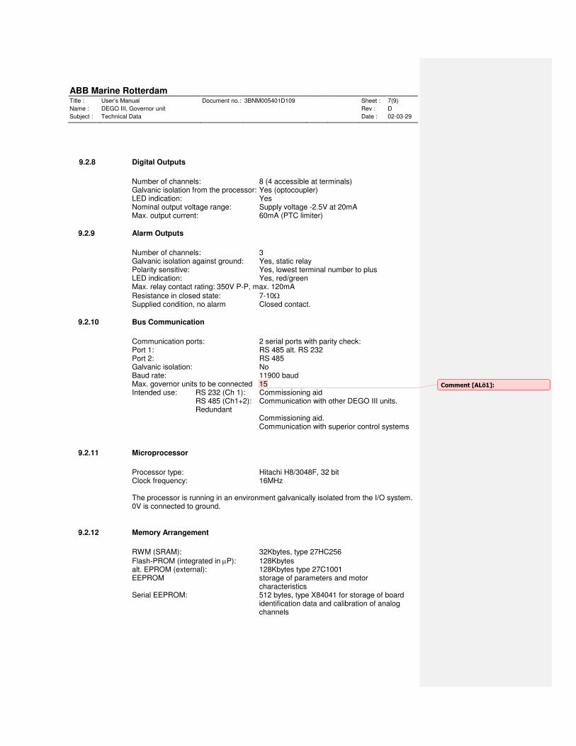
ABB Marine Rotterdam
Title : User’s Manual Document no.: 3BNM005401D109 Sheet : 7(9)
Name : DEGO III, Governor unit Rev : D
Subject : Technical Data Date : 02-03-29
9.2.8 Digital Outputs
Number of channels: 8 (4 accessible at terminals) Galvanic isolation from the processor: Yes (optocoupler) LED indication: Yes Nominal output voltage range: Supply voltage -2.5V at 20mA Max. output current: 60mA (PTC limiter)
9.2.9 Alarm Outputs
Number of channels: 3 Galvanic isolation against ground: Yes, static relay Polarity sensitive: Yes, lowest terminal number to plus LED indication: Yes, red/green Max. relay contact rating: 350V P-P, max. 120mA
Resistance in closed state: 7-10 Supplied condition, no alarm Closed contact.
9.2.10 Bus Communication
Communication ports: 2 serial ports with parity check: Port 1: RS 485 alt. RS 232 Port 2: RS 485 Galvanic isolation: No Baud rate: 11900 baud Max. governor units to be connected 15 Intended use: RS 232 (Ch 1): Commissioning aid
RS 485 (Ch1+2): Communication with other DEGO III units. Redundant
Commissioning aid. Communication with superior control systems
9.2.11 Microprocessor
Processor type: Hitachi H8/3048F, 32 bit Clock frequency: 16MHz The processor is running in an environment galvanically isolated from the I/O system. 0V is connected to ground.
9.2.12 Memory Arrangement
RWM (SRAM): 32Kbytes, type 27HC256
Flash-PROM (integrated in P): 128Kbytes alt. EPROM (external): 128Kbytes type 27C1001 EEPROM storage of parameters and motor
characteristics Serial EEPROM: 512 bytes, type X84041 for storage of board
identification data and calibration of analog channels
Comment [ALö1]:
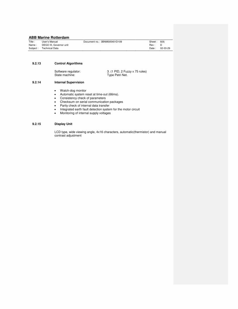
ABB Marine Rotterdam
Title : User’s Manual Document no.: 3BNM005401D109 Sheet : 8(9)
Name : DEGO III, Governor unit Rev : D
Subject : Technical Data Date : 02-03-29
9.2.13 Control Algorithms
Software regulator: 3. (1 PID, 2 Fuzzy x 75 rules) State machine: Type Petri Net.
9.2.14 Internal Supervision
Watch-dog monitor Automatic system reset at time-out (66ms). Consistency check of parameters Checksum on serial communication packages Parity check of internal data transfer Integrated earth fault detection system for the motor circuit Monitoring of internal supply voltages
9.2.15 Display Unit
LCD type, wide viewing angle, 4x16 characters, automatic(thermistor) and manual contrast adjustment
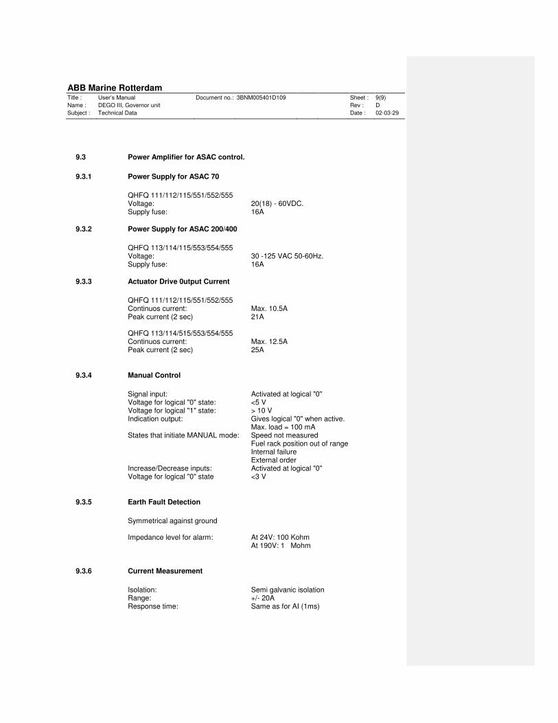
ABB Marine Rotterdam
Title : User’s Manual Document no.: 3BNM005401D109 Sheet : 9(9)
Name : DEGO III, Governor unit Rev : D
Subject : Technical Data Date : 02-03-29
9.3 Power Amplifier for ASAC control.
9.3.1 Power Supply for ASAC 70
QHFQ 111/112/115/551/552/555 Voltage: 20(18) - 60VDC. Supply fuse: 16A
9.3.2 Power Supply for ASAC 200/400
QHFQ 113/114/115/553/554/555 Voltage: 30 -125 VAC 50-60Hz. Supply fuse: 16A
9.3.3 Actuator Drive 0utput Current
QHFQ 111/112/115/551/552/555 Continuos current: Max. 10.5A Peak current (2 sec) 21A QHFQ 113/114/515/553/554/555 Continuos current: Max. 12.5A Peak current (2 sec) 25A
9.3.4 Manual Control
Signal input: Activated at logical "0" Voltage for logical "0" state: <5 V Voltage for logical "1" state: > 10 V Indication output: Gives logical "0" when active.
Max. load = 100 mA States that initiate MANUAL mode: Speed not measured
Fuel rack position out of range Internal failure External order
Increase/Decrease inputs: Activated at logical "0" Voltage for logical "0" state <3 V
9.3.5 Earth Fault Detection
Symmetrical against ground Impedance level for alarm: At 24V: 100 Kohm
At 190V: 1 Mohm
9.3.6 Current Measurement
Isolation: Semi galvanic isolation Range: +/- 20A Response time: Same as for AI (1ms)