MachXO2 Product Family Qualification · PDF fileLattice Semiconductor Corporation Doc....
40
Lattice Semiconductor Corporation Doc. #25-106923 Rev. L 1 MachXO2 Product Family Qualification Summary Lattice Document # 25 – 106923 February 2017
Transcript of MachXO2 Product Family Qualification · PDF fileLattice Semiconductor Corporation Doc....
Lattice Semiconductor Corporation Doc. #25-106923 Rev . L
1
MachXO2 Product Family Qualification Summary Lattice Document # 25 – 106923 February 2017
Lattice Semiconductor Corporation Doc. #25-106923 Rev . L
2
Dear Customer,
Enclosed is Lattice Semiconductor’s MachXO2 Product Family Qualification Report. This report was created to assist you in the decision making process of selecting and using our products. The
information contained in this report represents the entire qualification effort for this device family. The information is drawn from an extensive qualification program of the wafer technology and packaging assembly
processes used to manufacture our products. The program adheres to JEDEC and Automotive Industry standards for qualification of the technology and device packaging. This program ensures you only receive product that meets the most demanding requirements for Quality and Reliability.
Your feedback is valuable to Lattice. If you have suggestions to improve this report, or the data included, we encourage you to contact your Lattice representative.
Sincerely,
James M. Orr
Vice President, Corporate Quality Lattice Semiconductor Corporation

Lattice Semiconductor Corporation Doc. #25-106923 Rev . L
3
TABLE OF CONTENTS
1.0 INTRODUCTION ....................................................................................................................................4
2.0 LATTICE PRODUCT QUALIFICATION PROGRAM .................................................................................5
Figure 2.0.1 Lattice Standard Product Qualification Process Flow.................................................................6 Table 2.0.2 Standard Qualification Testing ................................................................................................8 Table 2.0.3 Industry Standard Qualification Testing for WLCSP Packages.....................................................9
3.0 QUALIFICATION DATA MACHXO2 PRODUCT FAMILY ....................................................................... 10
3.1 MACHXO2 PRODUCT FAMILY LIFE (HTOL) DATA ........................................................................................ 10 Table 3.1.1 MachXO2 Product Family Life Results using Pre-Production Wafer Fab Process Development Lots ................................................................................................................................................... 11 Table 3.1.2 MachXO2 Product Family Life Results Run on Production-Process Wafer Fabrication Lots ........ 12
3.2 MACHXO2 PRODUCT FAMILY HIGH TEMPERATURE RETENTION (HTRX) DATA ................................................... 13 Table 3.2.1 MachXO2 High Temperature Retention Results ...................................................................... 13
3.3 MACHXO2 PRODUCT FAMILY FLASH ENDURANCE CYCLING DATA ................................................................... 14 Table 3.3.1 MachXO2 Flash Extended Endurance Results ........................................................................ 14
3.4 MACHXO2 PRODUCT FAMILY – ESD AND LATCH UP DATA ........................................................................... 15 Table 3.4.1 MachXO2 ESD-HBM Data ................................................................................................... 15 Table 3.4.1 MachXO2 ESD-HBM Data (continued) ................................................................................... 16 Table 3.4.2 MachXO2 ESD-CDM Data ................................................................................................... 17 Table 3.4.2 MachXO2 ESD-CDM Data (continued)................................................................................... 18 Table 3.4.3 MachXO2 I/O Latch Up >100mA @ HOT (105°C) Data ............................................................ 19 Table 3.4.4 MachXO2 Vcc Latch Up >1.5X @ HOT (105°C) Data............................................................... 20
4.0 PACKAGE QUALIFICATION DATA FOR MACHXO2 PRODUCT FAMILY.............................................. 21
Table 4.0.1 Product-Package Qualification-By-Similarity Matrix .................................................................. 22 Table 4.02 WLCSP Package Qualification-By-Similarity Matrix................................................................... 23
4.1 MACHXO2 PRODUCT FAMILY SURFACE MOUNT PRECONDITIONING TESTING...................................................... 24 Table 4.1.1 Surface Mount Precondition Data .......................................................................................... 25
4.2 MACHXO2 PRODUCT FAMILY TEMPERATURE CYCLING DATA ......................................................................... 27 Table 4.2.1 Temperature Cycling Data.................................................................................................... 27 Table 4.3.1 Unbiased HAST Data .......................................................................................................... 29 Table 4.4.1 Biased HAST Data .............................................................................................................. 31 Table 4.5.1 MachXO2 High Temperature Storage Life Results................................................................... 33
5.0 BOARD LEVEL RELIABILITY (BLR) STRESS METHODS..................................................................... 35
Table 5.0.1 Slow-Temp Cycling, IPC-JEDEC9701 & JEDEC JESD22-A104 condition G, soak mode 2 ............ 36 Table 5.0.2 Bend Testing, IPC-JEDEC9702 & JEDEC JESD22-B113A ....................................................... 36 Table 5.0.3 Drop & Mechanical Shock Testing, IPC-JEDEC9703 & JEDEC JESD22-B111 / JESD-B104C....... 36
6.0 MACHXO2 PROCESS WAFER LEVEL RELIABILITY (WLR) ................................................................. 37
Table 6.0.1 Wafer Level Reliability (WLR) Results .................................................................................... 37
7.0 MACHXO2 SOFT ERROR RATE DATA ................................................................................................ 38
Table 7.0.1 MachXO2 MEASURED FITs / Mb ......................................................................................... 38
8.0 MACHXO2 ADDITIONAL FAMILY DATA .............................................................................................. 39
Table 8.0.1 MachXO2 Package Assembly Data – BGA , QFN & TQFP ...................................................... 39
9.0 REVISION HISTORY ............................................................................................................................ 40
Table 9.0.1 MachXO2 Product Family Qualification Summary revisions ...................................................... 40
Lattice Semiconductor Corporation Doc. #25-106923 Rev . L
4
1.0 INTRODUCTION
The MachXO2 family of ultra-low power, instant-on, non-volatile PLDs has six devices with densities ranging from
256 to 6864 Look-Up Tables (LUTs). In addition to LUT-based, low-cost programmable logic these devices feature
Embedded Block RAM (EBR), Distributed RAM, User Flash Memory (UFM), Phase Locked Loops (PLLs), pre-
engineered source synchronous I/O support, advanced configuration support including dual-boot capability and
hardened versions of commonly used functions such as SPI controller, I2C controller and timer/counter. These
features allow these devices to be used in low cost, high volume consumer and system applications.
The MachXO2 devices are designed on a 65nm non-volatile low power process. The device architecture has
several features such as programmable low swing differential I/Os and the ability to turn off I/O banks, on-chip
PLLs and oscillators dynamically. These features help manage static and dynamic power consumption resulting
in low static power for all members of the family.
The MachXO2 devices are available in three options – ultra low power (ZE) and high performance (HC and HE)
devices. The ultra-low power devices are offered in three speed grades -1, -2 and -3, with -3 being the fastest.
Similarly, the high-performance devices are offered in three speed grades: -4, -5 and -6, with -6 being the fastest.
HC devices have an internal linear voltage regulator which supports external VCC supply voltages of 3.3V or 2.5V.
ZE and HE devices only accept 1.2V as the external VCC supply voltage. With the exception of power supply
voltage all three types of devices (ZE, HC and HE) are functionally compatible and pin compatible with each other.
The MachXO2 PLDs are available in a broad range of advanced halogen-free packages ranging from the space
saving 2.5x2.5 mm WLCSP to the 23x23 mm fpBGA. MachXO2 devices support density migration within the same
package.
INDEX Return

Lattice Semiconductor Corporation Doc. #25-106923 Rev . L
5
2.0 LATTICE PRODUCT QUALIFICATION PROGRAM
Lattice Semiconductor Corp. maintains a comprehensive reliability qualification program to assure that each
product achieves its reliability goals. After initial qualification, the continued high reliability of Lattice products is
assured through ongoing monitor programs as described in Lattice Semiconductor’s Reliability Monitor Program
Procedure (Doc. #70-101667). All product qualification plans are generated in conformance with Lattice
Semiconductor’s Qualification Procedure (Doc. #70-100164) with failure analysis performed in conformance with
Lattice Semiconductor’s Failure Analysis Procedure (Doc. #70-100166). Both documents are referenced in Lattice
Semiconductor’s Quality Assurance Manual, which can be obtained upon request from a Lattice Semiconductor
sales office. Figure 2.1 shows the Product Qualification Process Flow.
If failures occur during qualification, an 8D process is used to find root cause and eliminate the failure mode from
the design, materials, or process. The effectiveness of any fix or change is validated through additional testing
as required. Final testing results are reported in the qualification reports.
Failure rates in this reliability report are expressed in FITs. Due to the very low failure rate of integrated circuits,
it is convenient to refer to failures in a population during a period of 109 device hours; one failure in 109 device
hours is defined as one FIT.
Product families are qualified based upon the requirements outlined in Table 2.2. In general, Lattice
Semiconductor follows the current Joint Electron Device Engineering Council (JEDEC) and Military Standard
testing methods. Lattice automotive products are qualified and characterized to the Automotive Electronics
Council (AEC) testing requirements and methods. Product family qualification will include products with a wide
range of circuit densities, package types, and package lead counts. Major changes to products, processes, or
vendors require additional qualification before implementation.
The MachXO2 family is the third generation FPGA product family and first 65 nm (CS200FL) Flash Technology
based product offering. The Lattice Semiconductor MachXO2 FPGA product family qualification efforts are based
on the first MachXO2 devices in the family per the Lattice Semiconductor Qualification Procedure, doc#70-
100164.
Lattice Semiconductor maintains a regular reliability monitor program. The current Lattice Reliability Monitor
Report can be found at Product Reliability Monitor Report.
INDEX Return

Lattice Semiconductor Corporation Doc. #25-106923 Rev . L
6
Figure 2.0.1 Lattice Standard Product Qualification Process Flow
This diagram represents the standard qualification flow used by Lattice to qualify new Product Families. The
target end market for the Product Family determines which flow options are used. The MachXO2 Product Family
was qualified using the Commercial / Industrial Qualification Option.
INDEX Return

Lattice Semiconductor Corporation Doc. #25-106923 Rev . L
7
INDEX Return
INDEX Return

Lattice Semiconductor Corporation Doc. #25-106923 Rev . L
8
Table 2.0.2 Standard Qualification Testing
TEST STANDARD TEST CONDITIONS
High Temperature Operating Life (HTOL)
JESD22-A108 ≥125°C Tj and max operating supplies
Human Body Model ESD (HBM)
JS-001 25°C (Technology/Device dependent Performance Targets)
Charged Device Model ESD (CDM)
JESD22-C101 25°C (Technology/Device dependent Performance Targets)
Latch-Up (LU) JESD78 Class II, +/-100mA trigger current and AMR
operating supplies
Accelerated Soft Error Testing (ASER)
JESD89 25°C, Nominal operating supplies
Surface Mount Pre-conditioning
(SMPC)
IPC/JEDEC J-STD-020D JESD-A113
Per appropriate MSL level per J-STD-020
High Temp Storage Life (HTSL)
JESD22-A103 Condition B
Temperature Cycling (TC)
JESD22-A104 Condition B, soak mode 2 (typical)
Temperature Humidity Bias, THB
(85/85) or Biased HAST (HAST)
JESD22-A101 JESD22-A110
85°C, 85 % RH, max operating supplies or
110°C, 85 % RH, max operating supplies or 130°C, 85 % RH, max operating supplies
Unbiased Temperature/Humidity
(UHAST)
JESD22-A118 110°C, 85 % RH or 130°C, 85 % RH
INDEX Return

Lattice Semiconductor Corporation Doc. #25-106923 Rev . L
9
Table 2.0.3 Industry Standard Qualification Testing for WLCSP Packages
STRESS TEST STANDARD TEST CONDITIONS
Slow-Temperature Cycling
JEDEC JESD22-A104 IPC-JEDEC9701A
Condition G, soak mode 2
(-40C to 125C, 7.5 min soak) 1-2 CPH for 3000 cycles
Bend Qualification
JEDEC JESD22-B113
IPC-JEDEC9702
200,000 bends of test boards at 1 to 3 Hz with maximum cross-head displacement of 4 mm
Drop Qualification Condition B
(Handheld apps)
JEDEC JESD22-B111 IPC-JEDEC9703
1500g drops 0.5 millisecond duration
half-sine pulse
Drop Qualification
Condition H (Shipping)
JEDEC JESD22-B104
IPC-JEDEC9703
2900g drops
0.3 millisecond duration half-sine pulse
INDEX Return
Lattice Semiconductor Corporation Doc. #25-106923 Rev . L
10
3.0 QUALIFICATION DATA MACHXO2 PRODUCT FAMILY
The MachXO2 devices are fabricated at Fujitsu on a 65nm non-volatile low power process, then assembled and
tested at ASEM in Malaysia, ASET in Kaohsiung, Taiwan, ATP in Philippines, ATT in Taiwan (WLCSP only), and
UTAC/NEPES in Singapore. The MachXO2 devices are available in three options – ultra low power (ZE) and high
performance (HC and HE) devices. The LCMXO2-1200 is the lead qualification vehicle for this product family.
Product Family: MachXO2
Packages offered: TQFP, μcBGA, csBGA, caBGA, ftBGA, fpBGA, QFN and WLCSP
Process Technology Node : 65 nm Flash
3.1 MachXO2 Product Family Life (HTOL) Data
High Temperature Operating Life (HTOL) Test
The High Temperature Operating Life test is used to thermally accelerate those wear out and failure mechanisms
that would occur as a result of operating the device continuously in a system application. Consistent with JEDEC
JESD22-A108 “Temperature, Bias, and Operating Life”, a pattern specifically designed to exercise the maximum
amount of circuitry is programmed into the device and this pattern is continuously exercised at specified voltages
as described in test conditions for each device type. The Early Life Failure Rate (ELFR) test uses large samples
sizes for a short duration (48 Hours) HTOL stress to determine the infant mortality rate of a device family.
MachXO2 Life Test (HTOL) Conditions:
Devices Stressed: LCMXO2
Pre-conditioning: All Flash cells Program/Erase cycled 10,000 times prior to HTOL stress.
Stress Duration: 48, 168, 500, 1000, 2000 hours.
Stress Conditions: MachXO2 (LCMXO2): HTOL Pattern, Vcc=1.26V, Vccio=3.47V TJUNCTION = >125°C
Method: Lattice Document # 87-101943 and JESD22-A108
The first 3 wafer lots of ELFR & HTOL stressed were pre-production process development lots.
INDEX Return
Lattice Semiconductor Corporation Doc. #25-106923 Rev . L
11
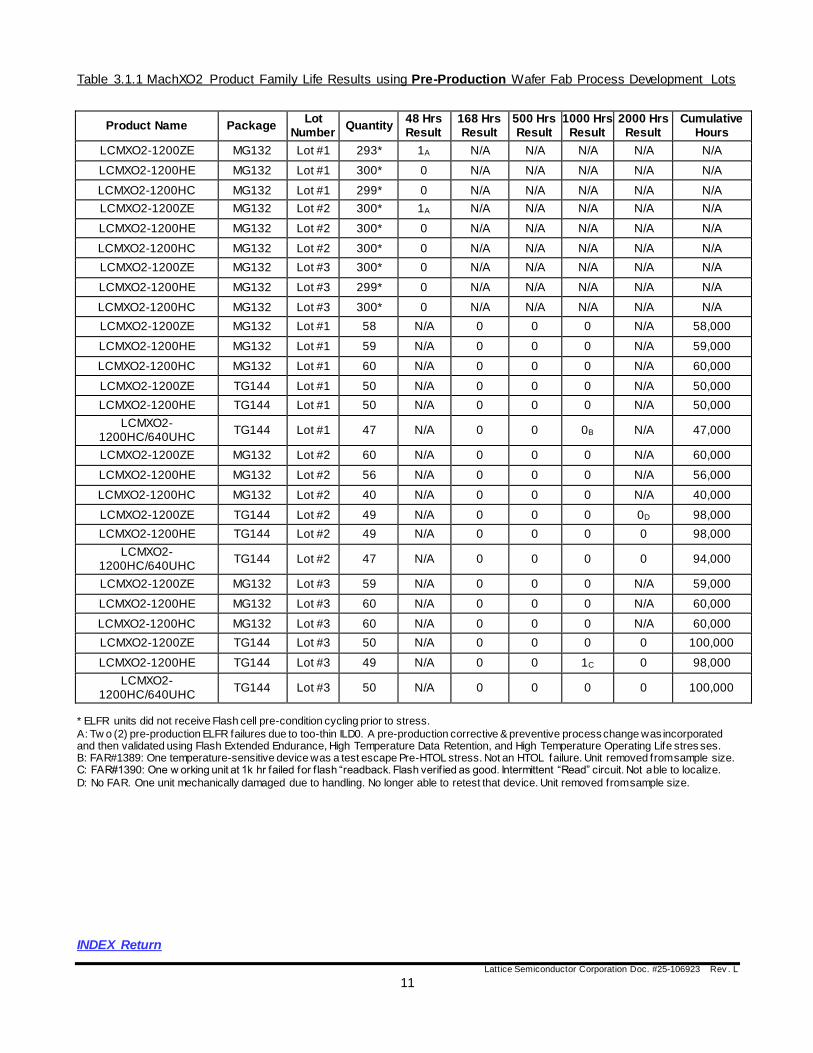
Table 3.1.1 MachXO2 Product Family Life Results using Pre-Production Wafer Fab Process Development Lots
Product Name Package Lot
Number Quantity
48 Hrs Result
168 Hrs Result
500 Hrs Result
1000 Hrs Result
2000 Hrs Result
Cumulative Hours
LCMXO2-1200ZE MG132 Lot #1 293* 1A N/A N/A N/A N/A N/A
LCMXO2-1200HE MG132 Lot #1 300* 0 N/A N/A N/A N/A N/A
LCMXO2-1200HC MG132 Lot #1 299* 0 N/A N/A N/A N/A N/A
LCMXO2-1200ZE MG132 Lot #2 300* 1A N/A N/A N/A N/A N/A
LCMXO2-1200HE MG132 Lot #2 300* 0 N/A N/A N/A N/A N/A
LCMXO2-1200HC MG132 Lot #2 300* 0 N/A N/A N/A N/A N/A
LCMXO2-1200ZE MG132 Lot #3 300* 0 N/A N/A N/A N/A N/A
LCMXO2-1200HE MG132 Lot #3 299* 0 N/A N/A N/A N/A N/A
LCMXO2-1200HC MG132 Lot #3 300* 0 N/A N/A N/A N/A N/A
LCMXO2-1200ZE MG132 Lot #1 58 N/A 0 0 0 N/A 58,000
LCMXO2-1200HE MG132 Lot #1 59 N/A 0 0 0 N/A 59,000
LCMXO2-1200HC MG132 Lot #1 60 N/A 0 0 0 N/A 60,000
LCMXO2-1200ZE TG144 Lot #1 50 N/A 0 0 0 N/A 50,000
LCMXO2-1200HE TG144 Lot #1 50 N/A 0 0 0 N/A 50,000
LCMXO2-1200HC/640UHC
TG144 Lot #1 47 N/A 0 0 0B N/A 47,000
LCMXO2-1200ZE MG132 Lot #2 60 N/A 0 0 0 N/A 60,000
LCMXO2-1200HE MG132 Lot #2 56 N/A 0 0 0 N/A 56,000
LCMXO2-1200HC MG132 Lot #2 40 N/A 0 0 0 N/A 40,000
LCMXO2-1200ZE TG144 Lot #2 49 N/A 0 0 0 0D 98,000
LCMXO2-1200HE TG144 Lot #2 49 N/A 0 0 0 0 98,000
LCMXO2-1200HC/640UHC
TG144 Lot #2 47 N/A 0 0 0 0 94,000
LCMXO2-1200ZE MG132 Lot #3 59 N/A 0 0 0 N/A 59,000
LCMXO2-1200HE MG132 Lot #3 60 N/A 0 0 0 N/A 60,000
LCMXO2-1200HC MG132 Lot #3 60 N/A 0 0 0 N/A 60,000
LCMXO2-1200ZE TG144 Lot #3 50 N/A 0 0 0 0 100,000
LCMXO2-1200HE TG144 Lot #3 49 N/A 0 0 1C 0 98,000
LCMXO2-1200HC/640UHC
TG144 Lot #3 50 N/A 0 0 0 0 100,000
* ELFR units did not receive Flash cell pre-condition cycling prior to stress.
A: Tw o (2) pre-production ELFR failures due to too-thin ILD0. A pre-production corrective & preventive process change was incorporated and then validated using Flash Extended Endurance, High Temperature Data Retention, and High Temperature Operating Life stres ses. B: FAR#1389: One temperature-sensitive device was a test escape Pre-HTOL stress. Not an HTOL failure. Unit removed from sample size. C: FAR#1390: One w orking unit at 1k hr failed for f lash “readback. Flash verif ied as good. Intermittent “Read” circuit. Not able to localize.
D: No FAR. One unit mechanically damaged due to handling. No longer able to retest that device. Unit removed from sample size.
INDEX Return

Lattice Semiconductor Corporation Doc. #25-106923 Rev . L
12
Table 3.1.2 MachXO2 Product Family Life Results Run on Production-Process Wafer Fabrication Lots
Product Name Package Lot Number Quantity 48 Hrs Result
168 Hrs Result
500 Hrs Result
1000 Hrs Result
2000 Hrs Result
Cumulative Hours
LCMXO2-1200ZE MG132 Lot #6 60 N/A 0 0 0 N/A 60,000
LCMXO2-1200HE MG132 Lot #6 60 N/A 0 0 0 N/A 60,000
LCMXO2-1200HC MG132 Lot #6 60 N/A 0 0 0 N/A 60,000
LCMXO2-1200ZE TG144 Lot #6 48 N/A 0 0 0 N/A 48,000
LCMXO2-1200HE TG144 Lot #6 49 N/A 0 0 0 N/A 49,000
LCMXO2-1200HC/640UHC
TG144 Lot #6 50 N/A 0 0 0 N/A 50,000
LCMXO2-7000ZE FTG256 Lot #1 40* N/A 0 0 0 0 80,000
LCMXO2-7000HE FTG256 Lot #1 40* N/A 0 0 0 0 80,000
LCMXO2-7000HC FTG256 Lot #1 40* N/A 0 0 0 0 80,000
LCMXO2-7000ZE TG144 Lot #1 50 N/A 0 0 0 0 100,000
LCMXO2-7000HE TG144 Lot #1 48 N/A 0 0 0 0 96,000
LCMXO2-7000HC TG144 Lot #1 48 N/A 0 0 0 0 96,000
LCMXO2-7000ZE FTG256 Lot #2 40* N/A 0 0 0 0 80,000
LCMXO2-7000HE FTG256 Lot #2 40* N/A 0 0 0 0 80,000
LCMXO2-7000HC FTG256 Lot #2 40* N/A 0 0 0 0 80,000
LCMXO2-7000ZE TG144 Lot #2 50 N/A 0 0 0 0 100,000
LCMXO2-7000HE TG144 Lot #2 48 N/A 0 0 0 0 96,000
LCMXO2-7000HC TG144 Lot #2 48 N/A 0 0 0 0 96,000
* FTG256 packaged units did not receive Flash cell pre-condition cycling prior to stress.
MachXO2 Product Family Life Results Run on Production-Process Wafer Fabrication Lots
INDEX Return
MachXO2 Cumulative Life Testing Device Hours = 1,391,000
MachXO2 Cumulative Result = 0 failures at 1000 & 2000 hours MachXO2 Long Term Failure Rate = 9 FIT FIT Assumptions: CL=60%, AE=0.7eV, Tjref=55C
MachXO2 ELFR (168Hrs) Cumulative Result / Sample Size = 0 / 859 MachXO2 HTOL (1000 Hrs) Cumulative Result / Sample Size = 0 / 859 MachXO2 HTOL (2000 Hrs) Cumulative Result / Sample Size = 0 / 532
Lattice Semiconductor Corporation Doc. #25-106923 Rev . L
13
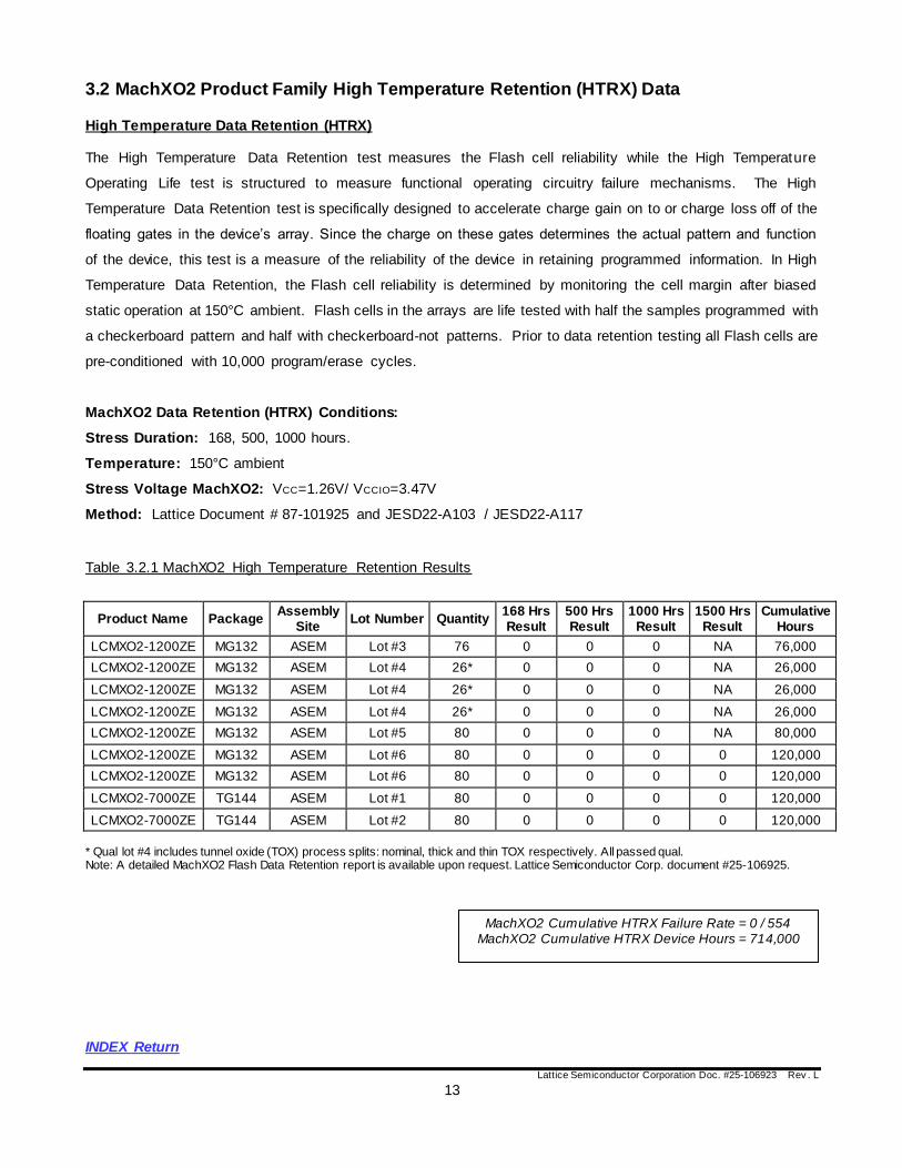
3.2 MachXO2 Product Family High Temperature Retention (HTRX) Data
High Temperature Data Retention (HTRX) The High Temperature Data Retention test measures the Flash cell reliability while the High Temperature
Operating Life test is structured to measure functional operating circuitry failure mechanisms. The High
Temperature Data Retention test is specifically designed to accelerate charge gain on to or charge loss off of the
floating gates in the device’s array. Since the charge on these gates determines the actual pattern and function
of the device, this test is a measure of the reliability of the device in retaining programmed information. In High
Temperature Data Retention, the Flash cell reliability is determined by monitoring the cell margin after biased
static operation at 150°C ambient. Flash cells in the arrays are life tested with half the samples programmed with
a checkerboard pattern and half with checkerboard-not patterns. Prior to data retention testing all Flash cells are
pre-conditioned with 10,000 program/erase cycles.
MachXO2 Data Retention (HTRX) Conditions:
Stress Duration: 168, 500, 1000 hours.
Temperature: 150°C ambient
Stress Voltage MachXO2: VCC=1.26V/ VCCIO=3.47V
Method: Lattice Document # 87-101925 and JESD22-A103 / JESD22-A117
Table 3.2.1 MachXO2 High Temperature Retention Results
Product Name Package Assembly
Site Lot Number Quantity
168 Hrs Result
500 Hrs Result
1000 Hrs Result
1500 Hrs Result
Cumulative Hours
LCMXO2-1200ZE MG132 ASEM Lot #3 76 0 0 0 NA 76,000
LCMXO2-1200ZE MG132 ASEM Lot #4 26* 0 0 0 NA 26,000
LCMXO2-1200ZE MG132 ASEM Lot #4 26* 0 0 0 NA 26,000
LCMXO2-1200ZE MG132 ASEM Lot #4 26* 0 0 0 NA 26,000
LCMXO2-1200ZE MG132 ASEM Lot #5 80 0 0 0 NA 80,000
LCMXO2-1200ZE MG132 ASEM Lot #6 80 0 0 0 0 120,000
LCMXO2-1200ZE MG132 ASEM Lot #6 80 0 0 0 0 120,000
LCMXO2-7000ZE TG144 ASEM Lot #1 80 0 0 0 0 120,000
LCMXO2-7000ZE TG144 ASEM Lot #2 80 0 0 0 0 120,000
* Qual lot #4 includes tunnel oxide (TOX) process splits: nominal, thick and thin TOX respectively. All passed qual. Note: A detailed MachXO2 Flash Data Retention report is available upon request. Lattice Semiconductor Corp. document #25-106925.
INDEX Return
MachXO2 Cumulative HTRX Failure Rate = 0 / 554 MachXO2 Cumulative HTRX Device Hours = 714,000

Lattice Semiconductor Corporation Doc. #25-106923 Rev . L
14
3.3 MachXO2 Product Family Flash Endurance Cycling Data Flash Extended Endurance testing measures the durability of the device through programming and erase cycles.
Endurance testing consists of repeatedly programming and erasing all cells in the array at 25°C ambient to
simulate programming cycles the user would perform. This test evaluates the integrity of the thin tunnel oxide
through which current passes to program the floating gate in each cell of the array.
MachXO2 Flash Extended Endurance Test Conditions:
Stress Duration: 1K, 10K, 20K, 50K, 100K Cycles
Temperature: 25°C ambient
Stress Voltage MachXO2: VCC=1.26V / VCCIO=3.47V
Method: Lattice Document # 70-104633 and JESD22-A117
Table 3.3.1 MachXO2 Flash Extended Endurance Results
The MachXO2 family uses the exact same Flash cell on all product densities and speed-power versions. The results above includes eight separate foundry lots of the same flash cell.
INDEX Return
Product Name Lot
Number Quantity
Cycling Temp
1K CYC
10K CYC
20K CYC
50K CYC
100K CYC
LCMXO2-1200ZE Lot #6 54 25C 0 0 0 0 0
LCMXO2-7000ZE Lot #1 60 25C 0 0 0 0 0
LCMXO2-7000ZE Lot #2 60 25C 0 0 0 0 0
LCMXO2-256ZE Lot #1 30 25C 0 0 0 0 0
LCMXO2-256ZE Lot #2 30 25C 0 0 0 0 0
LCMXO2-640ZE Lot #1 30 25C 0 0 0 0 0
LCMXO2-2000ZE Lot #1 30 25C 0 0 0 0 0
LCMXO2-4000ZE Lot #1 30 25C 0 0 0 0 0
MachXO2 Cumulative Unit Level Endurance Failure Rate = 0 / 324
Lattice Semiconductor Corporation Doc. #25-106923 Rev . L
15
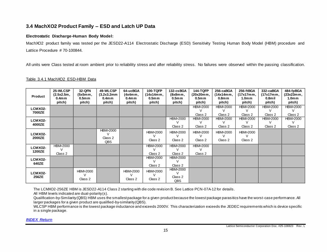
3.4 MachXO2 Product Family – ESD and Latch UP Data Electrostatic Discharge-Human Body Model:
MachXO2 product family was tested per the JESD22-A114 Electrostatic Discharge (ESD) Sensitivity Testing Human Body Model (HBM) procedure and
Lattice Procedure # 70-100844.
All units were Class tested at room ambient prior to reliability stress and after reliability stress. No failures were observed within the passing classification.
Table 3.4.1 MachXO2 ESD-HBM Data
Product
25-WLCSP (2.5x2.5m,
0.4mm
pitch)
32-QFN (5x5mm, 0.5mm
pitch)
49-WLCSP (3.2x3.2mm
0.4mm
pitch)
64-ucBGA (4x4mm, 0.4mm
pitch)
100-TQFP (14x14mm,
0.5mm
pitch)
132-csBGA (8x8mm, 0.5mm
pitch)
144-TQFP (20x20mm,
0.5mm
pitch)
256-caBGA (14x14mm,
0.8mm
pitch)
256-ftBGA (17x17mm,
1.0mm
pitch)
332-caBGA (17x17mm,
0.8mil
pitch)
484-fpBGA (23x23mm,
1.0mm
pitch)
LCMXO2-7000ZE
HBM>2000
V
Class 2
HBM>2000V
Class 2
HBM>2000V
Class 2
HBM>2000V
Class 2
HBM>2000V
Class 2
LCMXO2-
4000ZE
HBM>2000V
Class 2
HBM>2000V
Class 2
HBM>2000V
Class 2
HBM>2000V
Class 2
HBM>2000V
Class 2
HBM>2000V
Class 2
LCMXO2-2000ZE
HBM>2000V
Class 2
QBS
HBM>2000
V
Class 2
HBM>2000V
Class 2
HBM>2000V
Class 2
HBM>2000V
Class 2
HBM>2000V
Class 2
LCMXO2-1200ZE
HBM>2000V
Class 2
HBM>2000
V
Class 2
HBM>2000V
Class 2
HBM>2000V
Class 2
LCMXO2-
640ZE
HBM>2000
V
Class 2
HBM>2000V
Class 2
LCMXO2-256ZE
HBM>2000
V
Class 2
HBM>2000
V
Class 2
HBM>2000V
Class 2
HBM>2000V
Class 2
QBS
The LCMXO2-256ZE HBM is JESD22-A114 Class 2 starting with die code revision B. See Lattice PCN-07A-12 for details. All HBM levels indicated are dual-polarity (±). Qualification-by-Similarity (QBS) HBM uses the smallest package for a given product because the lowest package parasitics have the worst-case performance. All larger packages for a given product are qualified-by-similarity (QBS). WLCSP HBM performance is the lowest package inductance and exceeds 2000V. This characterization exceeds the JEDEC requirements which is device specific in a single package.
INDEX Return
Lattice Semiconductor Corporation Doc. #25-106923 Rev . L
16
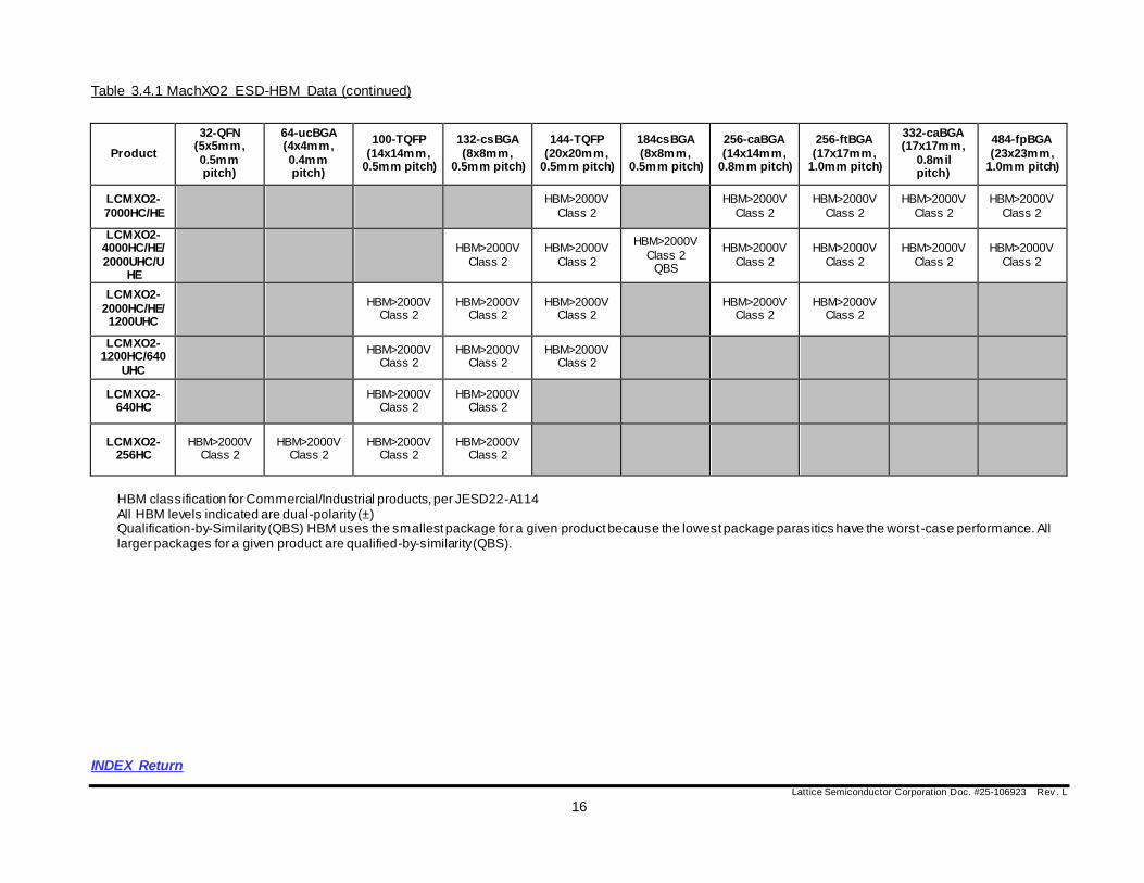
Table 3.4.1 MachXO2 ESD-HBM Data (continued)
Product
32-QFN (5x5mm,
0.5mm pitch)
64-ucBGA (4x4mm,
0.4mm pitch)
100-TQFP
(14x14mm, 0.5mm pitch)
132-csBGA
(8x8mm, 0.5mm pitch)
144-TQFP
(20x20mm, 0.5mm pitch)
184csBGA
(8x8mm, 0.5mm pitch)
256-caBGA
(14x14mm, 0.8mm pitch)
256-ftBGA
(17x17mm, 1.0mm pitch)
332-caBGA (17x17mm,
0.8mil pitch)
484-fpBGA
(23x23mm, 1.0mm pitch)
LCMXO2-
7000HC/HE
HBM>2000V
Class 2
HBM>2000V
Class 2
HBM>2000V
Class 2
HBM>2000V
Class 2
HBM>2000V
Class 2
LCMXO2-4000HC/HE/
2000UHC/UHE
HBM>2000V
Class 2
HBM>2000V
Class 2
HBM>2000V
Class 2 QBS
HBM>2000V
Class 2
HBM>2000V
Class 2
HBM>2000V
Class 2
HBM>2000V
Class 2
LCMXO2-
2000HC/HE/ 1200UHC
HBM>2000V
Class 2 HBM>2000V
Class 2 HBM>2000V
Class 2
HBM>2000V Class 2
HBM>2000V Class 2
LCMXO2-1200HC/640
UHC
HBM>2000V
Class 2 HBM>2000V
Class 2 HBM>2000V
Class 2
LCMXO2-640HC
HBM>2000V
Class 2 HBM>2000V
Class 2
LCMXO2-256HC
HBM>2000V Class 2
HBM>2000V Class 2
HBM>2000V Class 2
HBM>2000V Class 2
HBM classification for Commercial/Industrial products, per JESD22-A114 All HBM levels indicated are dual-polarity (±) Qualification-by-Similarity (QBS) HBM uses the smallest package for a given product because the lowest package parasitics have the worst-case performance. All larger packages for a given product are qualified-by-similarity (QBS).
INDEX Return

Lattice Semiconductor Corporation Doc. #25-106923 Rev . L
17
Electrostatic Discharge-Charged Device Model: MachXO2 product family was tested per the JESD22-C101, Field-Induced Charged-Device Model Test Method for Electrostatic-Discharge-Withstand
Thresholds of Microelectronic Components procedure and Lattice Procedure # 70-100844.
All units were Class tested at room ambient prior to reliability stress and after reliability stress. No failures were observed within the passing classification.
Table 3.4.2 MachXO2 ESD-CDM Data
Product
25-WLCSP (2.5x2.5m,
0.4mm pitch)
32-QFN (5x5mm,
0.5mm pitch)
49-WLCSP (3.2x3.2mm
0.4mm pitch)
64-ucBGA (4x4mm,
0.4mm pitch)
100-TQFP (14x14mm,
0.5mm pitch)
132-csBGA (8x8mm,
0.5mm pitch)
144-TQFP (20x20mm,
0.5mm pitch)
256-caBGA (14x14mm,
0.8mm pitch)
256-ftBGA (17x17mm,
1.0mm pitch)
332-caBGA (17x17mm,
0.8mil pitch)
484-fpBGA (23x23mm,
1.0mm pitch)
LCMXO2-7000ZE
CDM>1kV Class IV
CDM>1kV Class IV
CDM>1kV Class IV
CDM>1kV Class IV
CDM>1kV Class IV
LCMXO2-4000ZE
CDM>900V
Class III CDM>900V
Class III CDM>900V
Class III CDM>1kV Class IV
CDM>750V Class III
CDM>750V Class III
LCMXO2-2000ZE
CDM>1kV
Class IV QBS
CDM>1kV Class IV
CDM>1kV Class IV
CDM>1kV Class IV
CDM>1kV Class IV
CDM>1kV Class IV
LCMXO2-
1200ZE
CDM>1kV Class IV
QBS
CDM>1kV
Class IV
CDM>1kV
Class IV
CDM>1kV
Class IV
LCMXO2-640ZE
CDM>1kV Class IV
CDM>1kV Class IV
LCMXO2-256ZE
CDM>1kV Class IV
CDM>1kV Class IV
CDM>1kV Class IV
CDM>1kV Class IV
CDM classification for Commercial/Industrial products, per JESD22-C101 All CDM levels indicated are dual-polarity (±) Qualification-by-Similarity (QBS) CDM uses the smallest package for a given product because the lowest package parasitics have the worst-case performance. All larger packages for a given product are qualified-by-similarity (QBS).
INDEX Return
Lattice Semiconductor Corporation Doc. #25-106923 Rev . L
18
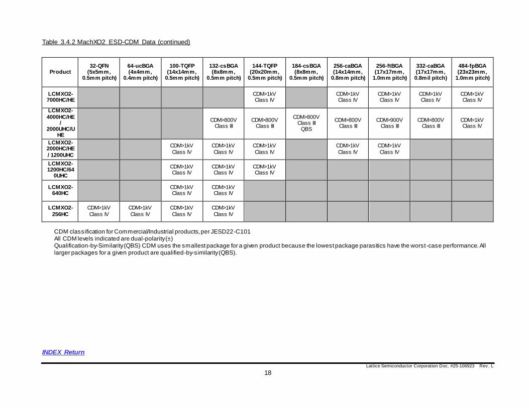
Table 3.4.2 MachXO2 ESD-CDM Data (continued)
Product 32-QFN
(5x5mm, 0.5mm pitch)
64-ucBGA (4x4mm,
0.4mm pitch)
100-TQFP (14x14mm,
0.5mm pitch)
132-csBGA (8x8mm,
0.5mm pitch)
144-TQFP (20x20mm,
0.5mm pitch)
184-csBGA (8x8mm,
0.5mm pitch)
256-caBGA (14x14mm,
0.8mm pitch)
256-ftBGA (17x17mm,
1.0mm pitch)
332-caBGA (17x17mm, 0.8mil pitch)
484-fpBGA (23x23mm,
1.0mm pitch)
LCMXO2-7000HC/HE
CDM>1kV Class IV
CDM>1kV Class IV
CDM>1kV Class IV
CDM>1kV Class IV
CDM>1kV Class IV
LCMXO2-
4000HC/HE/
2000UHC/UHE
CDM>800V
Class III CDM>800V
Class III
CDM>800V Class III
QBS
CDM>800V Class III
CDM>900V Class III
CDM>800V Class III
CDM>1kV Class IV
LCMXO2-2000HC/HE
/ 1200UHC
CDM>1kV
Class IV
CDM>1kV
Class IV
CDM>1kV
Class IV
CDM>1kV
Class IV
CDM>1kV
Class IV
LCMXO2-1200HC/64
0UHC
CDM>1kV Class IV
CDM>1kV Class IV
CDM>1kV Class IV
LCMXO2-640HC
CDM>1kV Class IV
CDM>1kV Class IV
LCMXO2-
256HC
CDM>1kV
Class IV
CDM>1kV
Class IV
CDM>1kV
Class IV
CDM>1kV
Class IV
CDM classification for Commercial/Industrial products, per JESD22-C101 All CDM levels indicated are dual-polarity (±) Qualification-by-Similarity (QBS) CDM uses the smallest package for a given product because the lowest package parasitics have the worst-case performance. All larger packages for a given product are qualified-by-similarity (QBS).
INDEX Return
Lattice Semiconductor Corporation Doc. #25-106923 Rev . L
19
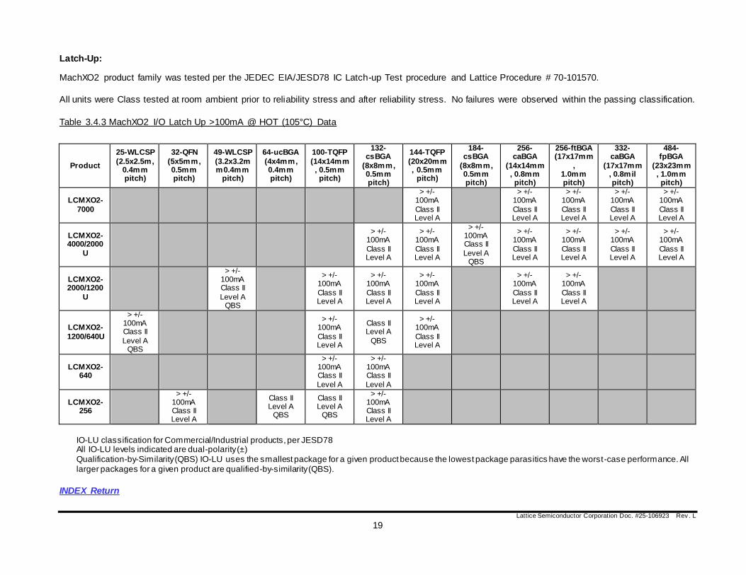
Latch-Up:
MachXO2 product family was tested per the JEDEC EIA/JESD78 IC Latch-up Test procedure and Lattice Procedure # 70-101570.
All units were Class tested at room ambient prior to reliability stress and after reliability stress. No failures were observed within the passing classification.
Table 3.4.3 MachXO2 I/O Latch Up >100mA @ HOT (105°C) Data
Product
25-WLCSP
(2.5x2.5m, 0.4mm pitch)
32-QFN
(5x5mm, 0.5mm pitch)
49-WLCSP
(3.2x3.2mm0.4mm
pitch)
64-ucBGA
(4x4mm, 0.4mm pitch)
100-TQFP
(14x14mm, 0.5mm pitch)
132-csBGA
(8x8mm, 0.5mm pitch)
144-TQFP
(20x20mm, 0.5mm
pitch)
184-csBGA
(8x8mm, 0.5mm pitch)
256-caBGA
(14x14mm, 0.8mm pitch)
256-ftBGA (17x17mm
, 1.0mm pitch)
332-caBGA
(17x17mm, 0.8mil pitch)
484-fpBGA
(23x23mm, 1.0mm pitch)
LCMXO2-
7000
> +/-100mA
Class II Level A
> +/-100mA
Class II Level A
> +/-100mA
Class II Level A
> +/-100mA
Class II Level A
> +/-100mA
Class II Level A
LCMXO2-4000/2000
U
> +/-100mA
Class II Level A
> +/-100mA
Class II Level A
> +/-100mA Class II
Level A QBS
> +/-100mA
Class II Level A
> +/-100mA
Class II Level A
> +/-100mA
Class II Level A
> +/-100mA
Class II Level A
LCMXO2-2000/1200
U
> +/-100mA Class II
Level A QBS
> +/-100mA
Class II Level A
> +/-100mA
Class II Level A
> +/-100mA
Class II Level A
> +/-100mA
Class II Level A
> +/-100mA
Class II Level A
LCMXO2-
1200/640U
> +/-100mA Class II
Level A QBS
> +/-100mA
Class II Level A
Class II Level A
QBS
> +/-100mA
Class II Level A
LCMXO2-640
> +/-100mA Class II
Level A
> +/-100mA Class II
Level A
LCMXO2-256
> +/-100mA Class II Level A
Class II Level A
QBS
Class II Level A
QBS
> +/-100mA Class II Level A
IO-LU classification for Commercial/Industrial products, per JESD78 All IO-LU levels indicated are dual-polarity (±) Qualification-by-Similarity (QBS) IO-LU uses the smallest package for a given product because the lowest package parasitics have the worst-case performance. All larger packages for a given product are qualified-by-similarity (QBS).
INDEX Return

Lattice Semiconductor Corporation Doc. #25-106923 Rev . L
20
Table 3.4.4 MachXO2 Vcc Latch Up >1.5X @ HOT (105°C) Data
Product
25-WLCSP (2.5x2.5m,
0.4mm pitch)
32-QFN (5x5mm, 0.5mm pitch)
49-WLCSP (3.2x3.2mm0.4mm
pitch)
64-ucBGA (4x4mm, 0.4mm pitch)
100-TQFP (14x14mm, 0.5mm pitch)
132-
csBGA (8x8mm, 0.5mm
pitch)
144-TQFP (20x20mm, 0.5mm
pitch)
184-
csBGA (8x8mm, 0.5mm
pitch)
256-
caBGA (14x14mm, 0.8mm
pitch)
256-ftBGA
(17x17mm,
1.0mm
pitch)
332-
caBGA (17x17mm
, 0.8mil
pitch)
484-
fpBGA (23x23mm, 1.0mm
pitch)
LCMXO2-
7000
> 1.5x Vcc
Class II
> 1.5x Vcc
Class II
> 1.5x Vcc
Class II
> 1.5x Vcc
Class II
> 1.5x Vcc
Class II
LCMXO2-4000/2000
U
> 1.5x Vcc Class II
> 1.5x Vcc Class II
> 1.5x Vcc Class II QBS
> 1.5x Vcc Class II
> 1.5x Vcc Class II
> 1.5x Vcc Class II
> 1.5x Vcc Class II
LCMXO2-2000/1200
U
> 1.5x Vcc Class II QBS
> 1.5x Vcc
Class II > 1.5x Vcc
Class II > 1.5x Vcc
Class II
> 1.5x Vcc Class II
> 1.5x Vcc Class II
LCMXO2-1200/640U
> 1.5x Vcc Class II QBS
> 1.5x Vcc
Class II Class II QBS
> 1.5x Vcc Class II
LCMXO2-
640
> 1.5x Vcc
Class II
> 1.5x Vcc
Class II
LCMXO2-
256
> 1.5x Vcc
Class II
Class II
QBS
Class II
QBS
> 1.5x Vcc
Class II
IO-LU classification for Commercial/Industrial products, per JESD78 All IO-LU levels indicated are dual-polarity (±) Qualification-by-Similarity (QBS) IO-LU uses the smallest package for a given product because the lowest package parasitics have the worst-case performance. All larger packages for a given product are qualified-by-similarity (QBS).
INDEX Return

Lattice Semiconductor Corporation Doc. #25-106923 Rev . L
21
4.0 PACKAGE QUALIFICATION DATA FOR MACHXO2 PRODUCT FAMILY
The MachXO2 product family is offered in TQFP, uc/cs/ca/ftBGA, fpBGA, QFN and WLCSP packages assembled
and tested at ASEM in Malaysia, ASET in Kaohsiung, Taiwan, ATT in Hsinchu, Taiwan, and UTAC/ NEPES in
Singapore. This report details the package qualification results of the initial MachXO2 product introductions.
Package qualification tests include Surface Mount Pre-Conditioning (SMPC), Temperature Cycling (T/C), Un-
biased HAST (UHAST), Biased HAST (BHAST) and High Temperature Storage (HTSL). Mechanical evaluation
tests include Scanning Acoustic Tomography (SAT) and visual package inspection. SMPC is used prior to all
other package stresses.
The generation and use of generic data applied across a family of packages emanating from one base assembly
process is a Family Qualification, or Qualification-by-Similarity. For the package stresses BHAST, UHAST and
HTSL, these are considered generic for a given Package Technology. T/C is considered generic up to an
evaluated die size + package size + 10%, for a given Package Technology. Surface Mount Pre-Conditioning
(SMPC) is considered generic up to an evaluated Peak Reflow temperature, for a given Package Technology.
The following table demonstrates the package stresses qualification matrix.
INDEX Return

Lattice Semiconductor Corporation Doc. #25-106923 Rev . L
22
Table 4.0.1 Product-Package Qualification-By-Similarity Matrix
Product-Package Combinations
Stress
Test
ASET Advanced Semiconductor Engineering, Malaysia (ASEM)
32-QFN (5x5mm,
0.5mm pitch)
32-QFN (5x5mm,
0.5mm pitch)
48-QFN (7x7mm,
0.5mm pitch)
84-QFN (7x7mm,
0.5mm pitch)
64-ucBGA (4x4mm,
0.4mm pitch)
100-TQFP (14x14mm,
0.5mm pitch)
132-csBGA (8x8mm,
0.5mm pitch)
144-TQFP (20x20mm,
0.5mm pitch)
184-csBGA
(8x8mm, 0.5mm pitch)
256-caBGA (14x14mm,
0.8mm pitch)
256-ftBGA (17x17mm,
1.0mm pitch)
332-caBGA
(17x17mm, 0.8mil pitch)
484-fpBGA (23x23mm,
1.0mm pitch)
LCMXO2-
7000
SMPC
Package
not offered
Package
not offered
Package not
offered
Package not
offered
Package not
offered
Package not
offered
Package not
offered
MSL3
Package
not offered
2 2 MSL3 MSL3
T/C 1K cycles 2 2 1K cycles 1K cycles
BHAST 1 2 2 2 264 hours
UHAST 1 2 2 2 264 hours
HTSL 1 2 2 2 1K hours
LCMXO2-
4000/2000U
SMPC
Package
not offered
Package
not offered
Package not
offered
Package not
offered
Package not
offered
Package not
offered
2 1 MSL3 2 2 2 3
T/C 2 1 1K cycles 2 2 2 3
BHAST 2 1 264 hours 2 2 2 3
UHAST 2 1 2 2 2 2 3
HTSL 2 1 1K cycles 2 2 2 3
LCMXO2-4000
SMPC
Package not offered
Package not offered
Package not offered
MSL3
Package not offered
Package not offered
Package not offered
Package not offered
Package not offered
Package not offered
Package not offered
Package not offered
Package not offered
T/C 700 cycles BHAST 4
UHAST 96 hours
HTSL 4
LCMXO2- 2000/1200U
SMPC
Package not offered
Package not offered
Package not offered
Package not offered
Package not offered
1 2 1
Package not offered
2 2
Package not offered
Package not offered
T/C 1 2 1 2 2
BHAST 1 2 1 2 2
UHAST 1 2 1 2 2
HTSL 1 2 1 2 2
LCMXO2-1200
SMPC
Package
not offered
MSL3
Package not
offered
Package not
offered
Package not
offered
Package not
offered
Package not
offered
Package
not offered
Package
not offered
Package not
offered
Package not
offered
Package
not offered
Package not
offered
T/C 700 cycles
BHAST 96 hours
UHAST N/A
HTSL 1k hours
LCMXO2- 1200/640U
SMPC
Package not offered
Package not offered
Package not offered
Package not offered
Package not offered
1 MSL3 MSL3
Package not offered
Package not offered
Package not offered
Package not offered
Package not offered
T/C 1 1K cycles 1K cycles
BHAST 1 264 hours 264 hours
UHAST 1 264 hours 264 hours
HTSL 1 1K hours 1K hours
LCMXO2- 640
SMPC
Package not offered
Package not offered
MXL3
Package not offered
Package not offered
1 2
Package not offered
Package not offered
Package not offered
Package not offered
Package not offered
Package not offered
T/C 700 cycles 1 2
BHAST 4 1 2
UHAST 96 hours 1 2
HTSL 4 1 2
LCMXO2- 256
SMPC MSL3
Package not offered
4
Package not offered
MSL3 1 2
Package not offered
Package not offered
Package not offered
Package not offered
Package not offered
Package not offered
T/C 1K cycle 4 1K cycle 1 2
BHAST 96 hours 4 2 1 2
UHAST N/A 4 2 1 2
HTSL 1K hours 4 1K hours 1 2
Notes: 1, 2, 3 & 4 – Qualified-by-similarity (QBS) from one of the other product-packages within the same packaging technology
INDEX Return
Lattice Semiconductor Corporation Doc. #25-106923 Rev . L
23
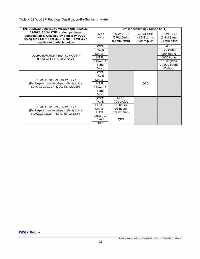
Table 4.02 WLCSP Package Qualification-By-Similarity Matrix
The LCMXO2-2000ZE, 49-WLCSP and LCMXO2-
1200ZE, 25-WLCSP product/package combination is Qualified-by-Similarity (QBS) using the LCMXO3L/XO3LF-4300, 81-WLCSP
qualification vehicle below.
Stress Tests
Amkor Technology Taiwan (ATT)
25-WLCSP (2.5x2.5mm, 0.4mm pitch)
49-WLCSP (3.2x3.2mm, 0.4mm pitch)
81-WLCSP (3.8x3.8mm, 0.4mm pitch)
LCMXO3L/XO3LF-4300, 81-WLCSP (Lead WLCSP qual vehicle)
SMPC
MSL1
T/C-B 700 cycles
UHAST 264 hours
HTSL 1000 hours
Slow-TC 1000 cycles
Bend 20,000 bends
Drop 30 drops
LCMXO2-2000ZE, 49-WLCSP (Package is qualified-by-similarity to the
LCMXO3L/XO3LF-4300, 81-WLCSP)
SMPC
QBS
T/C-B
UHAST
HTSL
Slow-TC
Bend
Drop
LCMXO2-1200ZE, 25-WLCSP (Package is qualified-by-similarity to the
LCMXO3L/XO3LF-4300, 81-WLCSP)
SMPC MSL1
T/C-B 700 cycles BHAST 96 hours
UHAST 96 hours HTSL 1000 hours
Slow-TC QBS Bend
Drop
INDEX Return
Lattice Semiconductor Corporation Doc. #25-106923 Rev . L
24
4.1 MachXO2 Product Family Surface Mount Preconditioning Testing The Surface Mount Preconditioning (SMPC) Test is used to model the surface mount assembly conditions during
component solder processing. All devices stressed through Temperature Cycling, Un-biased HAST and Biased
HAST were preconditioned. This preconditioning is consistent with JEDEC JESD22-A113 “Preconditioning
Procedures of Plastic Surface Mount Devices Prior to Reliability Testing”, Mois ture Sensitivity Level 3 (MSL3 or
MSL1, as applicable) package moisture sensitivity and dry-pack storage requirements.
Surface Mount Preconditioning (MSL3)
(10 Temperature Cycles, 24 hours bake @ 125°C, 30°C/60% RH, soak 192 hours, 260°C Reflow Simulation, 3
passes) performed before all package tests.
MSL3 Packages: TQFP, μcBGA, csBGA, caBGA, ftBGA, fpBGA and QFN
Surface Mount Preconditioning (MSL1)
(5 Temperature Cycles, 24 hours bake @ 125°C, 85°C/85% RH, soak 168 hours, 260°C Reflow Simulation, 3
passes) performed before all package tests.
MSL1 Packages: WLCSP
Method: Lattice Procedure # 70-103467, J-STD-020 and JESD22-A113
INDEX Return

Lattice Semiconductor Corporation Doc. #25-106923 Rev . L
25
Table 4.1.1 Surface Mount Precondition Data
Product Name Package Assembly
Site Lot Number Quantity # of Fails
Reflow Temperature
LCMXO2-256 32QFN ASET Lot #1 245** 0 260°C
LCMXO2-256 32QFN ASET Lot #2 246 0 260°C
LCMXO2-256 32QFN ASET Lot #3 246 0 260°C
LCMXO2-256 64ucBGA ASEM Lot #1 169 0 260°C
LCMXO2-256 64ucBGA ASEM Lot #2 169 0 260°C
LCMXO2-640 48QFN ASEM Lot #1 175 0 260°C
LCMXO2-640 48QFN ASEM Lot #2 175 0 260°C
LCMXO2-640 48QFN ASEM Lot #3 175 0 260°C
LCMXO2-1200 32QFN ASEM Lot #1 265 0 260°C
LCMXO2-1200 32QFN ASEM Lot #2 265 0 260°C
LCMXO2-1200 32QFN ASEM Lot #3 265 0 260°C
LCMXO2-1200 132csBGA ASEM Lot #1 308 0 260°C
LCMXO2-1200 132csBGA ASEM Lot #2 308 0 260°C
LCMXO2-1200 132csBGA ASEM Lot #3 308 0 260°C
LCMXO2-4000 84QFN ASEM Lot #1 265 0 260°C
LCMXO2-4000 84QFN ASEM Lot #2 264*** 0 260°C
LCMXO2-4000 84QFN ASEM Lot #3 265 0 260°C
LCMXO2-4000 184csBGA ASEM Lot #1 255 0 260°C
LCMXO2-4000 184csBGA ASEM Lot #2 255 0 260°C
LCMXO2-4000 184csBGA ASEM Lot #3 255 0 260°C
LCMXO2-4000 184csBGA ASEM Lot #4 80 0 260°C
LCMXO2-4000 184csBGA ASEM Lot #5 80 0 260°C
LCMXO2-7000 332caBGA ASEM Lot #1 77 0 260°C
LCMXO2-7000 332caBGA ASEM Lot #2 77 0 260°C
LCMXO2-1200/640U 144TQFP ASEM Lot #1 308 0 260°C
LCMXO2-1200/640U 144TQFP ASEM Lot #2 308 0 260°C
LCMXO2-1200/640U 144TQFP ASEM Lot #3 308 0 260°C
LCMXO2-7000 144TQFP ASEM Lot #1 77 0 260°C
LCMXO2-7000 144TQFP ASEM Lot #2 77 0 260°C
LCMXO2-7000 484fpBGA ASEM Lot #1 307* 0 250°C
LCMXO2-7000 484fpBGA ASEM Lot #2 306* 0 250°C
LCMXO2-7000 484fpBGA ASEM Lot #3 305* 0 250°C
LCMXO3LF-4300 81WLCSP ATT Lot #1 164 0 260°C
LCMXO3LF-4300 81WLCSP ATT Lot #2 164 0 260°C
LCMXO3LF-4300 81WLCSP ATT Lot #3 163 0 260°C
INDEX Return

Lattice Semiconductor Corporation Doc. #25-106923 Rev . L
26
Product Name Package Assembly
Site Lot Number Quantity # of Fails
Reflow Temperature
LCMXO2-1200ZE 25WLCSP ATT Lot #1 269** 0 260°C
LCMXO2-1200HE 25WLCSP ATT Lot #1 450 0 260°C
LCMXO2-1200HE 25WLCSP ATT Lot #2 450 0 260°C
LCMXO2-1200HE 25WLCSP ATT Lot #3 450 0 260°C
* 6 units had 1 corner solder ball knocked off due to handling damage. Sample size reduced accordingly for each of three assembly lots. ** 1 unit failed for “package damage“ due to handling damage. Sample size reduced by one. *** 1 unit failed w ith random silicon defect. Failure is unrelated to stress and sample size reduced by one.
INDEX Return
MachXO2 Cumulative SMPC Failure Rate = 0 / 9,298

Lattice Semiconductor Corporation Doc. #25-106923 Rev . L
27
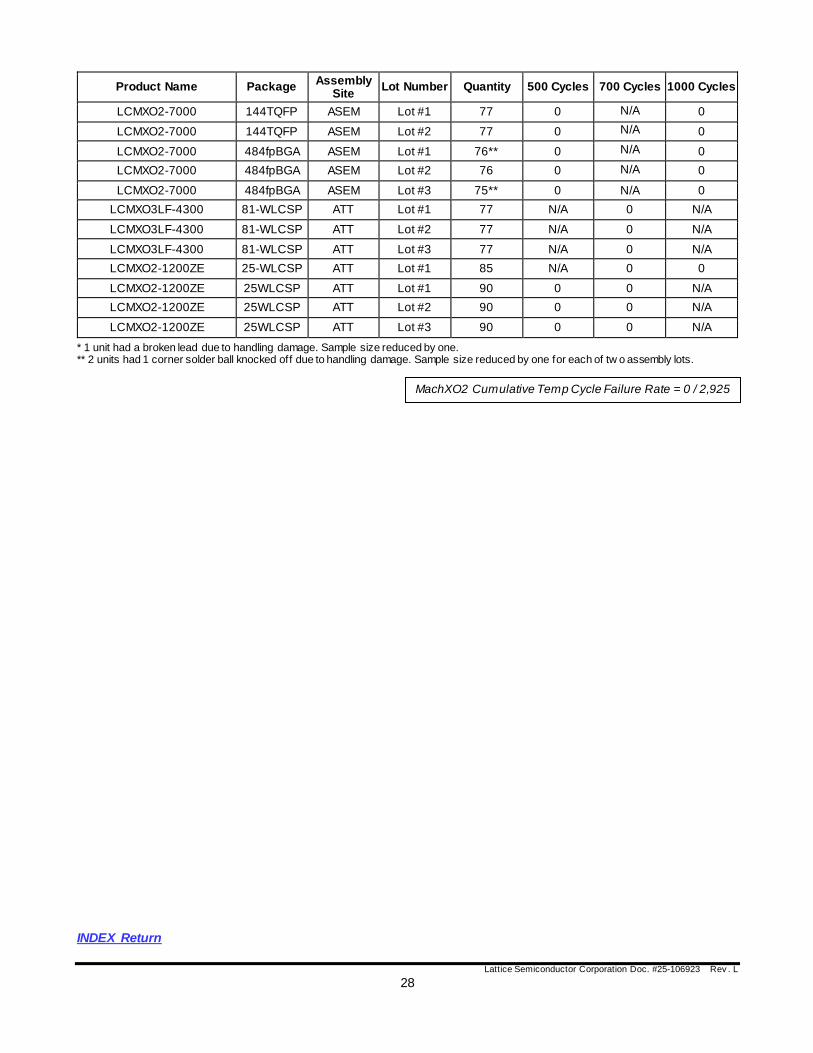
4.2 MachXO2 Product Family Temperature Cycling Data
The Temperature Cycling test is used to accelerate those failures resulting from mechanical stresses induced by
differential thermal expansion of adjacent films, layers and metallurgical interfaces in the die and package.
Devices are tested at 25°C after exposure to repeated cycling between -55°C and +125°C in an air environment
consistent with JEDEC JESD22-A104 “Temperature Cycling”, Condition B temperature cycling requirements .
Prior to Temperature Cycling testing, all devices are subjected to Surface Mount Preconditioning.
MSL3 Packages: TQFP, csBGA, QFN
MSL1 Packages: WLCSP
Stress Duration: 500, 700, 1000 cycles
Stress Conditions: Temperature cycling between -55°C to 125°C
Method: Lattice Procedure # 70-101568 and JESD22-A104, Condition B
Table 4.2.1 Temperature Cycling Data
Product Name Package Assembly
Site Lot Number Quantity 500 Cycles 700 Cycles 1000 Cycles
LCMXO2-256 32QFN ASET Lot #1 82 0 N/A 0
LCMXO2-256 32QFN ASET Lot #2 82 0 N/A 0
LCMXO2-256 32QFN ASET Lot #3 82 0 N/A 0
LCMXO2-256 64ucBGA ASEM Lot #1 80 0 N/A 0
LCMXO2-256 64ucBGA ASEM Lot #2 78 0 N/A 0
LCMXO2-640 48QFN ASEM Lot #1 80 N/A 0 0
LCMXO2-640 48QFN ASEM Lot #2 80 N/A 0 0
LCMXO2-640 48QFN ASEM Lot #3 80 N/A 0 0
LCMXO2-1200 32QFN ASEM Lot #1 80 N/A 0 0
LCMXO2-1200 32QFN ASEM Lot #2 80 N/A 0 0
LCMXO2-1200 32QFN ASEM Lot #3 80 N/A 0 0
LCMXO2-1200 132csBGA ASEM Lot #1 77 0 N/A 0
LCMXO2-1200 132csBGA ASEM Lot #2 77 0 N/A 0
LCMXO2-1200 132csBGA ASEM Lot #3 77 0 N/A 0
LCMXO2-4000 84QFN ASEM Lot #1 75 N/A 0 0
LCMXO2-4000 84QFN ASEM Lot #2 75 N/A 0 0
LCMXO2-4000 84QFN ASEM Lot #3 75 N/A 0 0
LCMXO2-4000 184csBGA ASEM Lot #1 78 0 N/A 0
LCMXO2-4000 184csBGA ASEM Lot #2 78 0 N/A 0
LCMXO2-4000 184csBGA ASEM Lot #3 78 0 N/A 0
LCMXO2-7000 332caBGA ASEM Lot #1 77 0 N/A 0
LCMXO2-7000 332caBGA ASEM Lot #2 77 0 N/A 0
LCMXO2-1200/640U 144TQFP ASEM Lot #1 77 0 N/A 0
LCMXO2-1200/640U 144TQFP ASEM Lot #2 77 0 N/A 0
LCMXO2-1200/640U 144TQFP ASEM Lot #3 76* 0 N/A 0
INDEX Return
Lattice Semiconductor Corporation Doc. #25-106923 Rev . L
28
Product Name Package Assembly
Site Lot Number Quantity 500 Cycles 700 Cycles 1000 Cycles
LCMXO2-7000 144TQFP ASEM Lot #1 77 0 N/A 0
LCMXO2-7000 144TQFP ASEM Lot #2 77 0 N/A 0
LCMXO2-7000 484fpBGA ASEM Lot #1 76** 0 N/A 0
LCMXO2-7000 484fpBGA ASEM Lot #2 76 0 N/A 0
LCMXO2-7000 484fpBGA ASEM Lot #3 75** 0 N/A 0
LCMXO3LF-4300 81-WLCSP ATT Lot #1 77 N/A 0 N/A
LCMXO3LF-4300 81-WLCSP ATT Lot #2 77 N/A 0 N/A
LCMXO3LF-4300 81-WLCSP ATT Lot #3 77 N/A 0 N/A
LCMXO2-1200ZE 25-WLCSP ATT Lot #1 85 N/A 0 0
LCMXO2-1200ZE 25WLCSP ATT Lot #1 90 0 0 N/A
LCMXO2-1200ZE 25WLCSP ATT Lot #2 90 0 0 N/A
LCMXO2-1200ZE 25WLCSP ATT Lot #3 90 0 0 N/A
* 1 unit had a broken lead due to handling damage. Sample size reduced by one. ** 2 units had 1 corner solder ball knocked off due to handling damage. Sample size reduced by one for each of tw o assembly lots.
INDEX Return
MachXO2 Cumulative Temp Cycle Failure Rate = 0 / 2,925
Lattice Semiconductor Corporation Doc. #25-106923 Rev . L
29
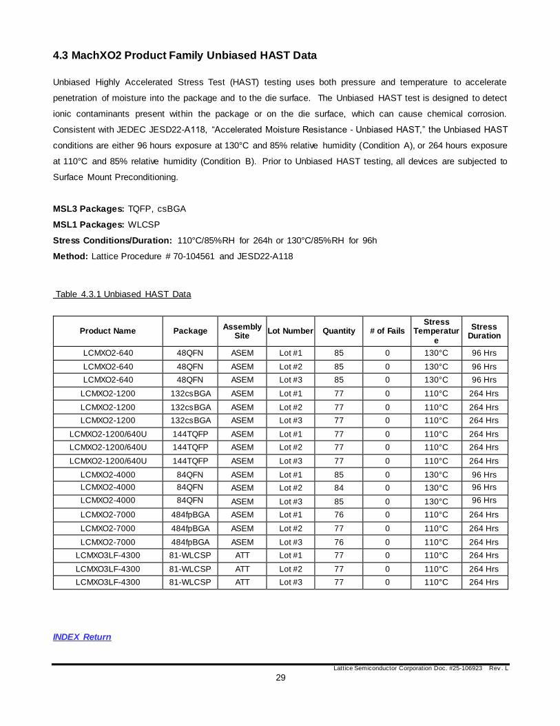
4.3 MachXO2 Product Family Unbiased HAST Data
Unbiased Highly Accelerated Stress Test (HAST) testing uses both pressure and temperature to accelerate
penetration of moisture into the package and to the die surface. The Unbiased HAST test is designed to detect
ionic contaminants present within the package or on the die surface, which can cause chemical corrosion.
Consistent with JEDEC JESD22-A118, “Accelerated Moisture Resistance - Unbiased HAST,” the Unbiased HAST
conditions are either 96 hours exposure at 130°C and 85% relative humidity (Condition A), or 264 hours exposure
at 110°C and 85% relative humidity (Condition B). Prior to Unbiased HAST testing, all devices are subjected to
Surface Mount Preconditioning.
MSL3 Packages: TQFP, csBGA
MSL1 Packages: WLCSP
Stress Conditions/Duration: 110°C/85%RH for 264h or 130°C/85%RH for 96h
Method: Lattice Procedure # 70-104561 and JESD22-A118
Table 4.3.1 Unbiased HAST Data
Product Name Package Assembly
Site Lot Number Quantity # of Fails
Stress Temperatur
e
Stress Duration
LCMXO2-640 48QFN ASEM Lot #1 85 0 130°C 96 Hrs
LCMXO2-640 48QFN ASEM Lot #2 85 0 130°C 96 Hrs
LCMXO2-640 48QFN ASEM Lot #3 85 0 130°C 96 Hrs
LCMXO2-1200 132csBGA ASEM Lot #1 77 0 110°C 264 Hrs
LCMXO2-1200 132csBGA ASEM Lot #2 77 0 110°C 264 Hrs
LCMXO2-1200 132csBGA ASEM Lot #3 77 0 110°C 264 Hrs
LCMXO2-1200/640U 144TQFP ASEM Lot #1 77 0 110°C 264 Hrs
LCMXO2-1200/640U 144TQFP ASEM Lot #2 77 0 110°C 264 Hrs
LCMXO2-1200/640U 144TQFP ASEM Lot #3 77 0 110°C 264 Hrs
LCMXO2-4000 84QFN ASEM Lot #1 85 0 130°C 96 Hrs
LCMXO2-4000 84QFN ASEM Lot #2 84 0 130°C 96 Hrs
LCMXO2-4000 84QFN ASEM Lot #3 85 0 130°C 96 Hrs
LCMXO2-7000 484fpBGA ASEM Lot #1 76 0 110°C 264 Hrs
LCMXO2-7000 484fpBGA ASEM Lot #2 77 0 110°C 264 Hrs
LCMXO2-7000 484fpBGA ASEM Lot #3 76 0 110°C 264 Hrs
LCMXO3LF-4300 81-WLCSP ATT Lot #1 77 0 110°C 264 Hrs
LCMXO3LF-4300 81-WLCSP ATT Lot #2 77 0 110°C 264 Hrs
LCMXO3LF-4300 81-WLCSP ATT Lot #3 77 0 110°C 264 Hrs
INDEX Return

Lattice Semiconductor Corporation Doc. #25-106923 Rev . L
30
Product Name Package Assembly
Site Lot Number Quantity # of Fails
Stress Temperature
Stress Duration
LCMXO2-1200ZE 25-WLCSP ATT Lot #1 85 0 110°C 264 Hrs
LCMXO2-1200ZE 25WLCSP ATT Lot #1 89 0 130°C 96 Hrs
LCMXO2-1200ZE 25WLCSP ATT Lot #2 90 0 130°C 96 Hrs
LCMXO2-1200ZE 25WLCSP ATT Lot #3 90 0 130°C 96 Hrs
INDEX Return
MachXO2 Cumulative Unbiased HAST failure Rate = 0 / 1,785
Lattice Semiconductor Corporation Doc. #25-106923 Rev . L
31
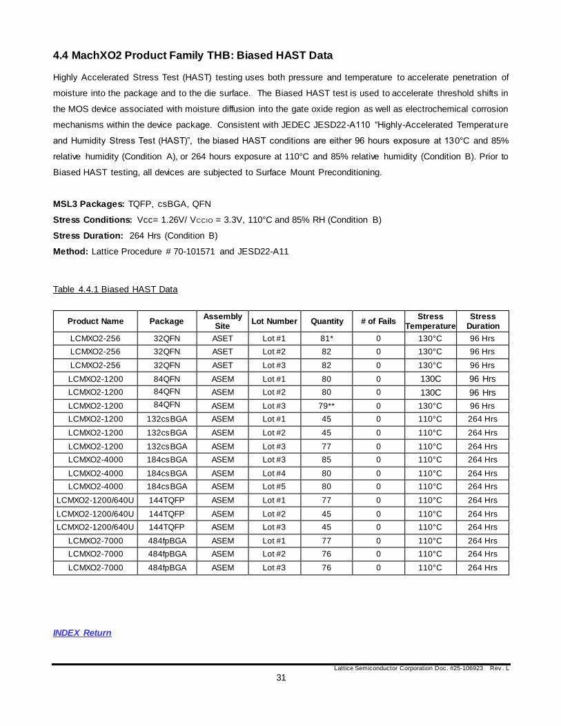
4.4 MachXO2 Product Family THB: Biased HAST Data Highly Accelerated Stress Test (HAST) testing uses both pressure and temperature to accelerate penetration of
moisture into the package and to the die surface. The Biased HAST test is used to accelerate threshold shifts in
the MOS device associated with moisture diffusion into the gate oxide region as well as electrochemical corrosion
mechanisms within the device package. Consistent with JEDEC JESD22-A110 “Highly-Accelerated Temperature
and Humidity Stress Test (HAST)”, the biased HAST conditions are either 96 hours exposure at 130°C and 85%
relative humidity (Condition A), or 264 hours exposure at 110°C and 85% relative humidity (Condition B). Prior to
Biased HAST testing, all devices are subjected to Surface Mount Preconditioning.
MSL3 Packages: TQFP, csBGA, QFN
Stress Conditions: Vcc= 1.26V/ VCCIO = 3.3V, 110°C and 85% RH (Condition B)
Stress Duration: 264 Hrs (Condition B)
Method: Lattice Procedure # 70-101571 and JESD22-A11
Table 4.4.1 Biased HAST Data
Product Name Package Assembly
Site Lot Number Quantity # of Fails
Stress Temperature
Stress Duration
LCMXO2-256 32QFN ASET Lot #1 81* 0 130°C 96 Hrs
LCMXO2-256 32QFN ASET Lot #2 82 0 130°C 96 Hrs
LCMXO2-256 32QFN ASET Lot #3 82 0 130°C 96 Hrs
LCMXO2-1200 84QFN ASEM Lot #1 80 0 130C 96 Hrs
LCMXO2-1200 84QFN ASEM Lot #2 80 0 130C 96 Hrs
LCMXO2-1200 84QFN ASEM Lot #3 79** 0 130°C 96 Hrs
LCMXO2-1200 132csBGA ASEM Lot #1 45 0 110°C 264 Hrs
LCMXO2-1200 132csBGA ASEM Lot #2 45 0 110°C 264 Hrs
LCMXO2-1200 132csBGA ASEM Lot #3 77 0 110°C 264 Hrs
LCMXO2-4000 184csBGA ASEM Lot #3 85 0 110°C 264 Hrs
LCMXO2-4000 184csBGA ASEM Lot #4 80 0 110°C 264 Hrs
LCMXO2-4000 184csBGA ASEM Lot #5 80 0 110°C 264 Hrs
LCMXO2-1200/640U 144TQFP ASEM Lot #1 77 0 110°C 264 Hrs
LCMXO2-1200/640U 144TQFP ASEM Lot #2 45 0 110°C 264 Hrs
LCMXO2-1200/640U 144TQFP ASEM Lot #3 45 0 110°C 264 Hrs
LCMXO2-7000 484fpBGA ASEM Lot #1 77 0 110°C 264 Hrs
LCMXO2-7000 484fpBGA ASEM Lot #2 76 0 110°C 264 Hrs
LCMXO2-7000 484fpBGA ASEM Lot #3 76 0 110°C 264 Hrs
INDEX Return

Lattice Semiconductor Corporation Doc. #25-106923 Rev . L
32
Product Name Package Assembly
Site Lot Number Quantity # of Fails
Stress Temperature
Stress Duration
LCMXO2-1200ZE 25WLCSP ATT Lot #1 90 0 130°C 96 Hrs
LCMXO2-1200ZE 25WLCSP ATT Lot #2 90 0 130°C 96 Hrs
LCMXO2-1200ZE 25WLCSP ATT Lot #3 90 0 130°C 96 Hrs
* 1 unit failed for “package damage“ due to handling damage. Sample size reduced by one. ** 1 unit failed for “package damage” due to EOS. Sample size reduced by one.
INDEX Return
MachXO2 Cumulative BHAST failure Rate = 0 / 1,562
Lattice Semiconductor Corporation Doc. #25-106923 Rev . L
33
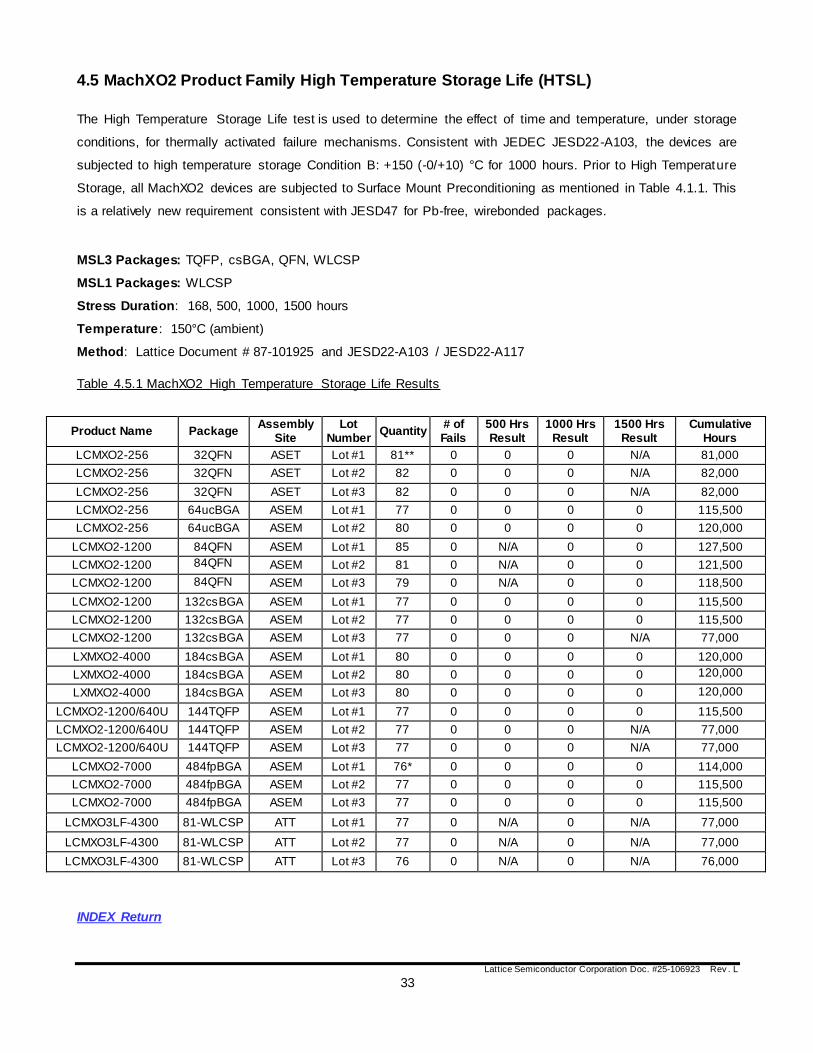
4.5 MachXO2 Product Family High Temperature Storage Life (HTSL)
The High Temperature Storage Life test is used to determine the effect of time and temperature, under storage
conditions, for thermally activated failure mechanisms. Consistent with JEDEC JESD22-A103, the devices are
subjected to high temperature storage Condition B: +150 (-0/+10) °C for 1000 hours. Prior to High Temperature
Storage, all MachXO2 devices are subjected to Surface Mount Preconditioning as mentioned in Table 4.1.1. This
is a relatively new requirement consistent with JESD47 for Pb-free, wirebonded packages.
MSL3 Packages: TQFP, csBGA, QFN, WLCSP
MSL1 Packages: WLCSP
Stress Duration: 168, 500, 1000, 1500 hours
Temperature: 150°C (ambient)
Method: Lattice Document # 87-101925 and JESD22-A103 / JESD22-A117
Table 4.5.1 MachXO2 High Temperature Storage Life Results
Product Name Package Assembly
Site Lot
Number Quantity
# of Fails
500 Hrs Result
1000 Hrs Result
1500 Hrs Result
Cumulative Hours
LCMXO2-256 32QFN ASET Lot #1 81** 0 0 0 N/A 81,000
LCMXO2-256 32QFN ASET Lot #2 82 0 0 0 N/A 82,000
LCMXO2-256 32QFN ASET Lot #3 82 0 0 0 N/A 82,000
LCMXO2-256 64ucBGA ASEM Lot #1 77 0 0 0 0 115,500
LCMXO2-256 64ucBGA ASEM Lot #2 80 0 0 0 0 120,000
LCMXO2-1200 84QFN ASEM Lot #1 85 0 N/A 0 0 127,500
LCMXO2-1200 84QFN ASEM Lot #2 81 0 N/A 0 0 121,500
LCMXO2-1200 84QFN ASEM Lot #3 79 0 N/A 0 0 118,500
LCMXO2-1200 132csBGA ASEM Lot #1 77 0 0 0 0 115,500
LCMXO2-1200 132csBGA ASEM Lot #2 77 0 0 0 0 115,500
LCMXO2-1200 132csBGA ASEM Lot #3 77 0 0 0 N/A 77,000
LXMXO2-4000 184csBGA ASEM Lot #1 80 0 0 0 0 120,000
LXMXO2-4000 184csBGA ASEM Lot #2 80 0 0 0 0 120,000
LXMXO2-4000 184csBGA ASEM Lot #3 80 0 0 0 0 120,000
LCMXO2-1200/640U 144TQFP ASEM Lot #1 77 0 0 0 0 115,500
LCMXO2-1200/640U 144TQFP ASEM Lot #2 77 0 0 0 N/A 77,000
LCMXO2-1200/640U 144TQFP ASEM Lot #3 77 0 0 0 N/A 77,000
LCMXO2-7000 484fpBGA ASEM Lot #1 76* 0 0 0 0 114,000
LCMXO2-7000 484fpBGA ASEM Lot #2 77 0 0 0 0 115,500
LCMXO2-7000 484fpBGA ASEM Lot #3 77 0 0 0 0 115,500
LCMXO3LF-4300 81-WLCSP ATT Lot #1 77 0 N/A 0 N/A 77,000
LCMXO3LF-4300 81-WLCSP ATT Lot #2 77 0 N/A 0 N/A 77,000
LCMXO3LF-4300 81-WLCSP ATT Lot #3 76 0 N/A 0 N/A 76,000
INDEX Return
Lattice Semiconductor Corporation Doc. #25-106923 Rev . L
34
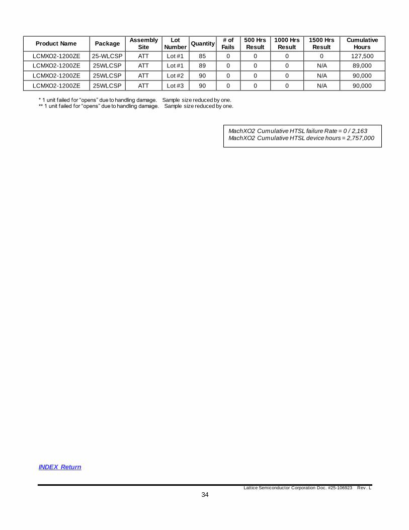
Product Name Package Assembly
Site Lot
Number Quantity
# of Fails
500 Hrs Result
1000 Hrs Result
1500 Hrs Result
Cumulative Hours
LCMXO2-1200ZE 25-WLCSP ATT Lot #1 85 0 0 0 0 127,500
LCMXO2-1200ZE 25WLCSP ATT Lot #1 89 0 0 0 N/A 89,000
LCMXO2-1200ZE 25WLCSP ATT Lot #2 90 0 0 0 N/A 90,000
LCMXO2-1200ZE 25WLCSP ATT Lot #3 90 0 0 0 N/A 90,000
* 1 unit failed for “opens” due to handling damage. Sample size reduced by one. ** 1 unit failed for “opens” due to handling damage. Sample size reduced by one.
INDEX Return
MachXO2 Cumulative HTSL failure Rate = 0 / 2,163
MachXO2 Cumulative HTSL device hours = 2,757,000

Lattice Semiconductor Corporation Doc. #25-106923 Rev . L
35
5.0 BOARD LEVEL RELIABILITY (BLR) STRESS METHODS
Reliability testing methods for surface mount electronic components in Wafer Level Chip Scale Packaging
(WLCSP) assembled onto printed circuit boards (PCB) are focused on the stresses observed by the manufacturing
and test processes and the applications associated with handheld electronic products. The handheld electronic
products fit into the consumer and portable market segments with products such as cameras, calculators, cell
phones, pagers, palm size PCs, PCMCIA cards, and the like.
Special daisy chain electronic components are constructed for board level reliability (BLR) testing to emulate as
closely as possible, the design, material sets and assembly processes of the actual product being qualified.
BLR PCB test boards are designed per JEDEC JESD22-B111 requirements: 1mm thick board with 1+6+1 stack
(8 layers) layup coated with OSP “Organic Surface Protection”. Units are arranged in a 3x5 configuration on the
board measuring 77mm x 132mm. One side provides VIP “Via-In-Pad” connections to the BGA and the flip side
provides NVIP “No-VIP” (surface-trace) connections. The design of pad to surface traces must avoid trace cracks.
BGA balls mount to NSMD “Non Solder Mask Defined” pads on the PCB.
Board Level Slow-Temperature Cycling (the slowest speed BLR stress) is intended to evaluate and compare the
PCB performance of surface mount electronics components in an environment that accelerates solder joint fatigue
and creep for handheld electronic products and applications. Pass/fail event detection is accomplished using
resistance measurements. All stress tests are performed in accordance with IPC-JEDEC9701 & JESD22-A104,
condition G, soak mode 2. Repeated slow-temperature cycling of printed circuit boards from
-40C to +125C, for up to 3,000 cycles. Handheld electronic products passing criteria is 1,000 cycles.
Board Level Cyclic Bend Test (the medium speed BLR stress) is intended to evaluate and c ompare the PCB
performance of surface mount electronics components in an environment that accelerates various assembly and
test operations and actual use conditions such as repeated key-presses in mobile phone during the life of the
product for handheld electronic products and applications. Pass/fail event detection is accomplished using
datalogging ‘opens’ detectors. All stress tests are performed in accordance with IPC-JEDEC9702 & JEDEC
JESD22-B113. Repeated bending of printed circuit boards at 1 to 3 Hz cyclic frequency for up to 200,000 cycles
with maximum cross-head displacement of 4 mm. Handheld electronic products passing criteria is 20,000 cycles.
Board Level Drop & Mechanical Shock (the instantaneous BLR stress) is intended to evaluate and compare PCB
drop performance of surface mount electronic components for handheld electronic product applications in an
accelerated test environment determine the compatibility of the component(s) to withstand moderately severe
shocks as a result of suddenly applied forces or abrupt change in motion produced by handling,
INDEX Return

Lattice Semiconductor Corporation Doc. #25-106923 Rev . L
36
transportation or field operation. Further, handheld electronic products are more prone to being dropped during
their useful service life because of their size and weight. Pass/fail event detection is accomplished using
datalogging ‘opens’ detectors. All stress tests are performed in accordance with IPC-JEDEC9703 & JEDEC
JESD22-B111 (drop) and JESD-B104 (shock). Repeated drop testing of printed circuit boards at 1500g, 0.5
millisecond half-sine pulse and 2900g, 0.3 millisecond half-sine pulse for up to 1,000 drops. Handheld electronic
products passing criteria is 30 drops.
All devices stressed through Board Level Reliability Slow-TC, Bend and Drop Testing were preconditioned. This
preconditioning is consistent with JEDEC JESD22-A113F “Preconditioning Procedures of Plastic Surface Mount
Devices Prior to Reliability Testing”, Moisture Sensitivity Level 1 (MSL1) and 1x 260C Solder Reflow.
Slow-TC 1st fail is >1,000 cycles = PASS
Bend testing did not fail after 20,000 cycles = PASS
Drop testing did not fail after 30 drops = PASS
Mechanical Shock testing 1st fail is >30 drops = PASS
Table 5.0.1 Slow-Temp Cycling, IPC-JEDEC9701 & JEDEC JESD22-A104 condition G, soak mode 2
Assembly Site Package Die Size
(mm)
Ball Pitch (mm)
Temp Range (C) & Dwell time (min)
Cycles per hour
Sample Size
1st Fail (Cycles)
N (63.2%) (Cycles)
% Fails @ *1k/3k Cycles
UTAC / NEPES 25-
WLCSP 2.546 x 2.492
0.4 -40C to +125C & 7.5 min at each
endpoint 1.2
100/lot x 3 lots
1,568 2,785 67.3%
ATT 81-
WLCSP 3.8 x 3.8 0.4
-40C to +125C & 5 min at each
endpoint 1.5
247/lot x 3 lots
N/A N/A *0
Table 5.0.2 Bend Testing, IPC-JEDEC9702 & JEDEC JESD22-B113A
Assembly Site Package Die Size
(mm)
Ball Pitch (mm)
Cross-head Displacement &
Strain
Frequency (Hz)
Sample Size
1st Fail (Cycles)
N (63.2%) (Cycles)
% Fails @ 200k
Cycles
UTAC / NEPES 25-
WLCSP 2.546 x 2.492
0.4 4 mm & 1100 ppm strain tensile and
compressive 1-3
36/lot x 3 lots
No fails No fails No fails
ATT 81-
WLCSP 3.8 x 3.8 0.4
4 mm & 1100 ppm strain tensile and
compressive 1-3
71/lot x 3 lots
98,000 N/A 7.0
Table 5.0.3 Drop & Mechanical Shock Testing, IPC-JEDEC9703 & JEDEC JESD22-B111 / JESD-B104C
Assembly Site Package Die Size Ball
Pitch (mm)
Drop & Shock Waveform
Sample Size 1st Fail (Drops)
N (63.2%) (Drops)
% Fails @ 1000 Drops
UTAC / NEPES 25-
WLCSP 2.546 x 2.492
0.4 1500 g, 0.5 ms half-sine pulse
96/lot x 3 lots VIP
No fails @ 30 drops
TBD TBD
UTAC / NEPES 25-
WLCSP 2.546 x 2.492
0.4 2900 g, 0.3 ms half-sine pulse
45/lot x 1 lots
644 N/A 2.2%
ATT 81-
WLCSP 3.8 x 3.8 0.4
0.3 ms half-sine pulse
180/lot x 3 lots
257 N/A 16.1
INDEX Return
Lattice Semiconductor Corporation Doc. #25-106923 Rev . L
37
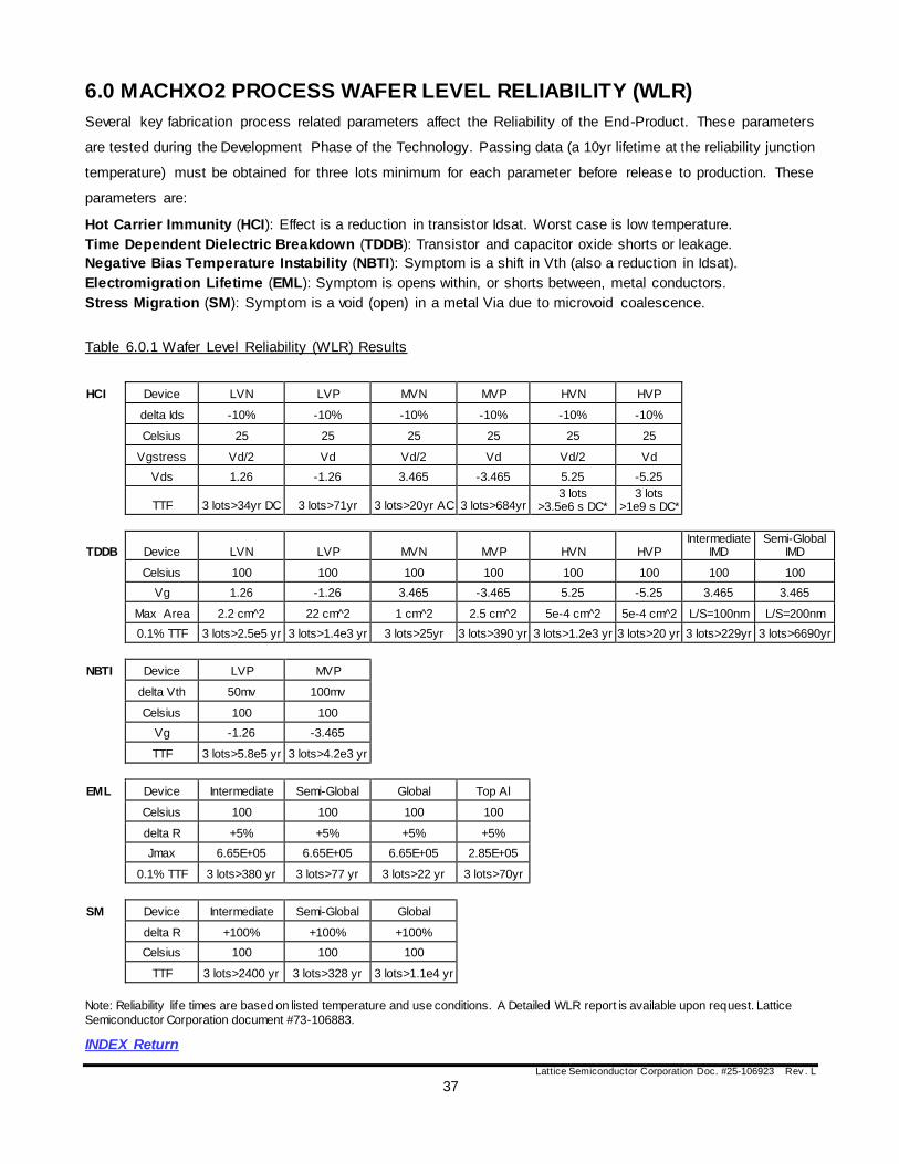
6.0 MACHXO2 PROCESS WAFER LEVEL RELIABILITY (WLR)
Several key fabrication process related parameters affect the Reliability of the End-Product. These parameters
are tested during the Development Phase of the Technology. Passing data (a 10yr lifetime at the reliability junction
temperature) must be obtained for three lots minimum for each parameter before release to production. These
parameters are:
Hot Carrier Immunity (HCI): Effect is a reduction in transistor Idsat. Worst case is low temperature.
Time Dependent Dielectric Breakdown (TDDB): Transistor and capacitor oxide shorts or leakage.
Negative Bias Temperature Instability (NBTI): Symptom is a shift in Vth (also a reduction in Idsat).
Electromigration Lifetime (EML): Symptom is opens within, or shorts between, metal conductors.
Stress Migration (SM): Symptom is a void (open) in a metal Via due to microvoid coalescence.
Table 6.0.1 Wafer Level Reliability (WLR) Results
HCI Device LVN LVP MVN MVP HVN HVP
delta Ids -10% -10% -10% -10% -10% -10%
Celsius 25 25 25 25 25 25
Vgstress Vd/2 Vd Vd/2 Vd Vd/2 Vd
Vds 1.26 -1.26 3.465 -3.465 5.25 -5.25
TTF 3 lots>34yr DC 3 lots>71yr 3 lots>20yr AC 3 lots>684yr 3 lots
>3.5e6 s DC* 3 lots
>1e9 s DC*
TDDB Device LVN LVP MVN MVP HVN HVP Intermediate
IMD Semi-Global
IMD
Celsius 100 100 100 100 100 100 100 100
Vg 1.26 -1.26 3.465 -3.465 5.25 -5.25 3.465 3.465
Max Area 2.2 cm^2 22 cm^2 1 cm^2 2.5 cm^2 5e-4 cm^2 5e-4 cm^2 L/S=100nm L/S=200nm
0.1% TTF 3 lots>2.5e5 yr 3 lots>1.4e3 yr 3 lots>25yr 3 lots>390 yr 3 lots>1.2e3 yr 3 lots>20 yr 3 lots>229yr 3 lots>6690yr
NBTI Device LVP MVP
delta Vth 50mv 100mv
Celsius 100 100
Vg -1.26 -3.465
TTF 3 lots>5.8e5 yr 3 lots>4.2e3 yr
EML Device Intermediate Semi-Global Global Top Al
Celsius 100 100 100 100
delta R +5% +5% +5% +5%
Jmax 6.65E+05 6.65E+05 6.65E+05 2.85E+05
0.1% TTF 3 lots>380 yr 3 lots>77 yr 3 lots>22 yr 3 lots>70yr
SM Device Intermediate Semi-Global Global
delta R +100% +100% +100%
Celsius 100 100 100
TTF 3 lots>2400 yr 3 lots>328 yr 3 lots>1.1e4 yr
Note: Reliability life times are based on listed temperature and use conditions. A Detailed WLR report is available upon request. Lattice
Semiconductor Corporation document #73-106883.
INDEX Return
Lattice Semiconductor Corporation Doc. #25-106923 Rev . L
38
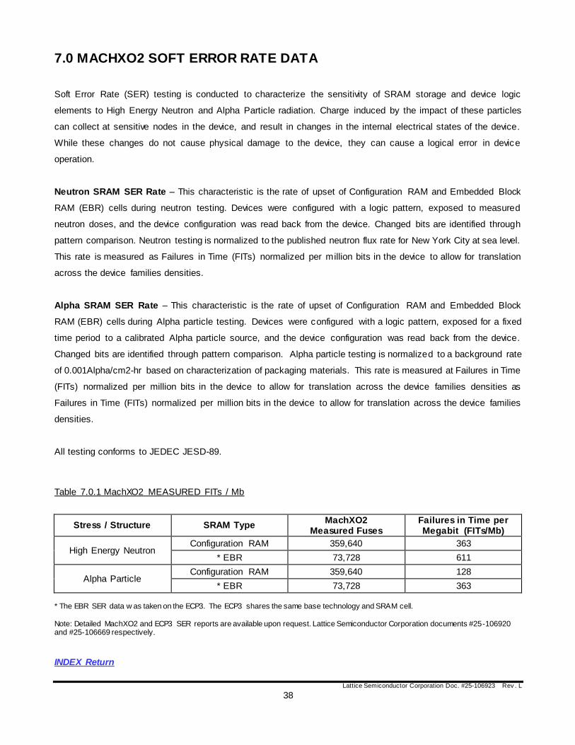
7.0 MACHXO2 SOFT ERROR RATE DATA
Soft Error Rate (SER) testing is conducted to characterize the sensitivity of SRAM storage and device logic
elements to High Energy Neutron and Alpha Particle radiation. Charge induced by the impact of these particles
can collect at sensitive nodes in the device, and result in changes in the internal electrical states of the device.
While these changes do not cause physical damage to the device, they can cause a logical error in device
operation.
Neutron SRAM SER Rate – This characteristic is the rate of upset of Configuration RAM and Embedded Block
RAM (EBR) cells during neutron testing. Devices were configured with a logic pattern, exposed to measured
neutron doses, and the device configuration was read back from the device. Changed bits are identified through
pattern comparison. Neutron testing is normalized to the published neutron flux rate for New York City at sea level.
This rate is measured as Failures in Time (FITs) normalized per million bits in the device to allow for translation
across the device families densities.
Alpha SRAM SER Rate – This characteristic is the rate of upset of Configuration RAM and Embedded Block
RAM (EBR) cells during Alpha particle testing. Devices were configured with a logic pattern, exposed for a fixed
time period to a calibrated Alpha particle source, and the device configuration was read back from the device.
Changed bits are identified through pattern comparison. Alpha particle testing is normalized to a background rate
of 0.001Alpha/cm2-hr based on characterization of packaging materials. This rate is measured at Failures in Time
(FITs) normalized per million bits in the device to allow for translation across the device families densities as
Failures in Time (FITs) normalized per million bits in the device to allow for translation across the device families
densities.
All testing conforms to JEDEC JESD-89.
Table 7.0.1 MachXO2 MEASURED FITs / Mb
Stress / Structure SRAM Type MachXO2
Measured Fuses Failures in Time per Megabit (FITs/Mb)
High Energy Neutron Configuration RAM 359,640 363
* EBR 73,728 611
Alpha Particle Configuration RAM 359,640 128
* EBR 73,728 363
* The EBR SER data w as taken on the ECP3. The ECP3 shares the same base technology and SRAM cell.
Note: Detailed MachXO2 and ECP3 SER reports are available upon request. Lattice Semiconductor Corporation documents #25-106920 and #25-106669 respectively.
INDEX Return

Lattice Semiconductor Corporation Doc. #25-106923 Rev . L
39
8.0 MACHXO2 ADDITIONAL FAMILY DATA
Table 8.0.1 MachXO2 Package Assembly Data – BGA, QFN & TQFP
Package Attributes /
Assembly Sites UTAC / NEPES ASET ATT ASEM ASEM ASEM ASEM
Die Family (Product Line) LCMXO2 LCMXO2 LCMXO2 LCMXO2 LCMXO2 LCMXO2 LCMXO2
Fabrication Process
Technology
65nm CMOS
(CS200FL)
65nm CMOS
(CS200FL)
65nm CMOS
(CS200FL)
65nm CMOS
(CS200FL)
65nm CMOS
(CS200FL)
65nm CMOS
(CS200FL)
65nm CMOS
(CS200FL)
Package Assembly Site Singapore Kaohsiung, Taiw an Taiw an Malaysia Malaysia Malaysia Malaysia
Package Type WLCSP QFN WLCSP QFN ucBGA, csBGA,
caBGA & ftBGA TQFP fpBGA
Ball/Lead Counts 25 32 49 32, 48, 84 64, 132, 184, 256/332
& 256 respectively 100 & 144 484
Die Preparation /
Singulation w afer saw w afer saw / full cut n/a
w afer saw / full
cut w afer saw / full cut
w afer saw / full
cut w afer saw / full cut
Die Attach Material n/a Hitachi EN-4900F n/a
Furukaw a
NEX130CTX/
CRM1076DS
Ablebond 2100A Ablebond 3230 Ablebond 2100A
Mold Compound
Supplier/ID n/a
Sumitomo
EME-G631H n/a
Sumitomo
G770SFL
Hitachi
CEL9750ZHF10ALKU
Hitachi
CEL9510HF 10
Hitachi
9750HF10 AKLU
Wire Bond Material n/a Gold (Au) n/a PCC Gold (Au) Gold (Au) Gold (Au)
Wire Bond Methods n/a Thermosonic Ball n/a Thermosonic Ball Thermosonic Ball Thermosonic Ball Thermosonic Ball
Substrate Material or Lead
Frame n/a CU C194 n/a ???
Bismaleimide Triazine
HL83X Series n/a
Bismaleimide
Triazine
HL83X Series
Lead Finish Plating or
BGA Ball SAC405 Matte Sn SAC305 Matte Sn SAC305 Matte Sn SAC305
Marking Laser Laser Laser Laser Laser Laser Laser
INDEX Return

Lattice Semiconductor Corporation Doc. #25-106923 Rev . L
40
9.0 REVISION HISTORY
Table 9.0.1 MachXO2 Product Family Qualification Summary revisions
Date Revision Section Change Summary
April 2011 A --- Initial document release.
October 2011 B 3.0 Silicon &
4.0 Package
Added LCMXO2-7000 qual data. Also added LCMXO2-
256/640/2000/4000/7000 ESD/LU data.
March 2012 C
3.1 Life Test 3.4 ESD/LU 3.4 ESD/LU
Added LCMXO2-7000 HTOL 2000 hour data. Added ESD/LU data for the caBGA packages. Added ESD/LU data in support of PCN 07A-12 in section
3.4 for the LCMXO2-256ZE device.
October 2012 D
3.0 QUAL DATA 3.4 ESD/LU
4.0 PACKAGE
4.1 SMPC 4.2 TC
4.4 BHAST
4.5 HTSL 7.0 FAMILY DATA
Added LCMXO2-256-32QFN qual data. Updated SMPC, TC, BHAST, ESD-HBM/CDM, LU data and additional
family data.
November 2012 E 3.4 ESD/LU Updated ESD-MM data.
February 2013 F
4.1 SMPC 4.2 T/C
4.4 BHAST
4.5 HTSL
Added LCMXO2-4000-184csBGA qual data. Updated SMPC, TC, BHAST, HTSL data.
July 2013 G
Updated LCMXO2-4000-184csBGA qual data with the latest results. Added LCMXO2-1200-25WLCSP Board Level Reliability (BLR) stress methods & data. Corrected typographical errors in prior data sets.
October 2015 H Oct. 2015 Added 49-WLCSP package to the XO2 Product Family.
December 2015 I Update document to include expanded device/package coverage.
May 2016 J Added 25-WLCSP package to the XO2 Product Family.
October 2016 K Added ASEM assembled QFN packages to the XO2 Product Family
February 2017 L Added ATT assembled WLCSP packages to the XO2
Product Family
Lattice Semiconductor Corporation 5555 NE Moore Court Hillsboro, Oregon 97124 U.S.A. Telephone: (503) 268-8000 www.latticesemi.com © 2017 Lattice Semiconductor Corp. All Lattice trademarks, registered trademarks, patents, and disclaimers are listed at www.latticesemi.com/legal. All other brand or product names are trademarks or registered trademarks of their respective holders. The specifications and information herein are subject to change without notice.
www.latticesemi.com