
Lxfedder/phd_thesis/Ch3_Fedder...=1 j m ij _ q i j (3.3) V = 1 2 n X i =1 j k ij q i j (3.4) F = 1 2...
91
Transcript of Lxfedder/phd_thesis/Ch3_Fedder...=1 j m ij _ q i j (3.3) V = 1 2 n X i =1 j k ij q i j (3.4) F = 1 2...

67
Chapter 3
Lumped-Parameter Modeling
3.1 Introduction
In this chapter, we will present an overview of a select group of lumped-parameter
models for surface microsystems. We will discuss micromechanical equations of motion,
squeeze-lm damping, spring constants, electrostatic actuation, and capacitive position
sensing. Our analyses are focused on application to the micromechanical testbed, which
is the topic of following chapters.
3.2 Mechanical Equations of Motion
Micromechanical structures can be divided into discrete elements that are modeled
using rigid-body dynamics. Finite-element analysis is used to determine the mechanical
modes that are within the bandwidth of the feedback and external forces. Some structural
elements can be modeled simply as rigid body mass, while other models may include the
eects of bending, torsion, axial, and shear stress.
A mechanical system with n degrees of freedom can be described in terms of n
generalized coordinates, q1; q2; : : : ; qn, and time, t. A general method of determining the
equations of motion involves use of Lagrange's equation [55].
d
dt
@L
@ _qi
@L
@qi= Qnc;i ; i = 1; : : : ; n (3.1)
where L = TV is the Lagrangian operator, T is the total kinetic energy of the system, and
V is the potential energy of the system, arising from conservative forces. Non-conservative

68
forces, such as dissipative forces, are lumped in the terms Qnc;i. If only viscous damping
terms (damping proportional to velocity) are present, then Lagrange's equation can be
written asd
dt
@L
@ _qi
@L
@qi+@F
@qi= Qext;i ; i = 1; : : : ; n (3.2)
where F is the Rayleigh dissipation function, and Qext;i is an external generalized force
associated with the coordinate qi. In general, the kinetic energy, potential energy, and
dissipation function have the forms
T =1
2
nXi=1
nXj=1
mij _qi _qj (3.3)
V =1
2
nXi=1
nXj=1
kijqiqj (3.4)
F =1
2
nXi=1
nXj=1
Bij _qi _qj (3.5)
where mij are inertia coecients, kij are stiness coecients, and Bij are damping coe-
cients.
We will apply Lagrange's equation to the example, shown in Figure 3.1, of a rigid
rectangular plate suspended by four springs located at the plate's corners1. Generalized
coordinates are chosen to be the three Cartesian directions2, x, y, and z, and the three
angles of rotation, , , and . Potential energy stored in the springs is determined by
summing the contributions of each spring. Making small angle approximations, we nd
V = 2kxx
2 + kyy2 + kzz
2 + kzL2
ky2 + kzL
2
kx2 + kyL
2
kx 2
(3.6)
where kx, ky, and kz are spring constants in the x, y, and z directions, respectively. The
dimensions Lkx and Lky are the distances along the x and y axis from the centroid of the
plate to the springs3. We assume that the spring force varies linearly with displacement;
however, nonlinear spring forces can be modeled by substituting stiness coecients that
are functions of position into Equation (3.6). If we assume massless springs, then the kinetic
energy is
T =1
2
m _x2 +m _y2 +m _z2 + I _
2 + I _2 + I _ 2
(3.7)
1The micromechanical testbed, discussed in chapters 46, has this kind of suspension.2In this general discussion, we choose the origin of the axes to be at the center of the plate. However,
when we analyze specic micromechanical elements, we will choose the z-axis origin to be at the substrate.The variable z will then be used to describe vertical displacement of a plate from its rest (zero mechanicalpotential) position.
3In the example illustrated in Figure 3.1, the springs are located at Lkx = Lx=2 and Lky = Ly=2.

69
kyL
Lkx
Ly
Lx
xθ
y φ
z
ψ
plate mass(rigid body)
spring(spring constants,
)kx , ky , kz
Figure 3.1: Schematic of a rigid rectangular plate, with dimensions Lx Ly . Springsare attached at distances Lkx and Lky along the x-axis and y-axis, respectively, from thecentroid of the plate.

70
where m is the plate mass and the mass moments of inertia of the plate are given by
I =m
12L2
y (3.8)
I =m
12L2
x (3.9)
I =m
12
L2
x + L2
y
(3.10)
We will assume viscous damping of the plate can be expressed by the dissipation function,
F =1
2
Bx _x
2 +By _y2 +Bz _z
2 +B _2 +B _
2 + B _ 2
(3.11)
where Bx, By , Bz , B , B, B , are the damping coecients of the six modes. The expres-
sions for kinetic energy, potential energy, and dissipation function of the mass-spring-damper
system are substituted into Equation (3.2) and then solved for each of the six coordinates,
resulting in the following equations of motion:
Fx = mx+Bx _x+ kxx (3.12)
Fy = my +By _y + kyy (3.13)
Fz = mz +Bz _z + kzz (3.14)
= I +B _ + kzL2
ky (3.15)
= I +B _+ kzL2
kx (3.16)
= I + B _ + kyL2
kx (3.17)
where Fx, Fy , Fz , , , and are external forces and torques that act on the plate. Values
for the stiness and damping coecients can be determined numerically using nite-element
analysis or approximated by analytic formulas, as discussed in the following two sections.
Most of the simulation and modeling described in this thesis involves vertical
motion of a suspended plate. Therefore, we will often refer to the vertical equations of
motion, Equations (3.14)(3.16), which can be expressed in the alternative form
Fz = mz + 2z!z _z + !2zz
(3.18)
= I + 2! _ + !2
(3.19)
= I+ 2! _+ !2
(3.20)
where !z , ! , and ! are resonant frequencies and z , , and are dimensionless damping
factors of the z, , and modes, respectively. In general, the resonant frequency, !i, and

71
zo
zplate
substrate
v
FB squeeze film
Figure 3.2: Cross-section schematic of a plate with an air gap, zo, above the substrate,illustrating the squeeze-lm damping arising from vertical motion of the plate with velocity,v. Pressure in the squeeze lm produces a force, FB, which is proportional to the velocity.
damping factor, i, of mode i are given by
!i =
skimi
(3.21)
i =Bi
2pkimi
(3.22)
where ki is the stiness coecient and mi is the inertia coecient (mass for translational
modes or moment of inertia for rotational modes) of mode i. Eects of spring mass can be
included by introducing eective inertia coecients to adjust the resonant frequency.
3.3 Squeeze-Film Damping
Viscous air damping is the dominant dissipation mechanism for microstructures
that operate at atmospheric pressure. Squeeze-lm damping, illustrated in Figure 3.2, arises
from vertical motion which creates a pressure in the thin lm of air between the plate and
substrate. Detailed reports on general squeeze-lm damping are given in [5658]4; a review
of squeeze-lm damping in micromechanical accelerometers is given by Starr [62]. We will
provide a brief review of squeeze-lm damping, and apply the results to vertical motion of
a 400 m 400 m plate with a 2 m air gap.
3.3.1 Simplifying Assumptions for Viscous Flow
Continuum uid mechanics can be used to analyze squeeze-lm damping if the air
gap is much larger than the mean-free-path, , of the air molecules. Mean-free-path of a
4Laterally moving microstructures experience a dierent form of air damping, Couette damping, in thegap under the structure. Several papers report on analytic models of Couette damping for microstructures[5961].

72
gas is expressed as
=1p
2 d2on(3.23)
where d2o is the collision cross-section of the gas molecules, and n is the molecular density,
which, for an ideal gas, is given by
n =P
kBT(3.24)
where P is pressure of the squeeze lm, kB is Boltzmann's constant, and T is absolute
temperature. For air at atmospheric pressure and T=300K, the mean-free-path is 65 nm.
The 2 m air gap dimension is about 31 larger than the mean-free-path, so the air can be
modeled approximately as a viscous uid. At pressures below about 25 T, the mean-free-
path is greater than 2 m and the gas lm dynamics must be treated as an ensemble of
molecules, not as a viscous uid. In this molecular- ow regime, the air damping will decrease
dramatically with decreasing pressure, and structural damping will eventually dominate the
losses.
We describe the viscous- ow regime with the Navier-Stokes equation, which, when
several assumptions are made, can be reduced to [62]
@2P
@x2+@2P
@y2=
12
z3o
@(z)
@t(3.25)
where P is pressure of the squeeze lm, is the viscosity of air5, zo is the air-gap height,
and z is the plate displacement. Equation (3.25) is valid if the squeeze lm is isothermal
and has small pressure variations, and if the plate undergoes small displacements with small
velocities.
Large relative displacements with respect to the air gap will increase the damping.
A plate displacement of zo/4 results in a 10 % increase in damping relative to the value
calculated using the small-displacement assumption [62]. Air velocity in the gap can be
considered small if the Reynolds number, Re, is much less than 1, where
Re = v zo
(3.26)
and is the density of air6, and v is the air velocity. With a 2 m air gap, and a plate
oscillation frequency of 1 kHz and oscillation amplitude of 1 m, the Reynolds number is
very small (Re=0.0009). To rst order, both the Reynolds number and squeeze number are
independent of pressure, since the air viscosity and density vary linearly with pressure.
5The viscosity of air is 1.79 105 Pa-s at atmospheric pressure and T=288K [46].6The density of air is 1.22 kg/m3 at atmospheric pressure and T=288K [46].

73
zo
zplate
substrate
v
Ly
Lx /2x /2−L 0 x
dx
dx
Figure 3.3: Schematic of a plate for one-dimensional analysis of squeeze-lm damping. Thedrawing is not to scale, since we assume Ly Lx.
3.3.2 One-Dimensional Analysis
We will analyze squeeze-lm damping of the plate shown in Figure 3.3, where the
plate length, Ly, in the y-direction is much larger than the length, Lx in the x-direction.
The squeeze lm is modeled with a one-dimensional version of Equation (3.25):
@2P
@x2=
12 v
z3o(3.27)
Double integration of Equation (3.27) and application of the pressure boundary conditions
at the edges of the plate gives
P =6 v
z3o
x2 L2
x
4
!(3.28)
where P is the pressure dierence from ambient pressure. The average pressure dierence
across the plate is L2
xv=z3
o , and the total force from damping exerted on the plate is
FB = Ly L
3x
z3o
!v (3.29)

74
The squeeze-lm damping coecient for a rectangular plate is
Bz = KBz(Lx=Ly)Ly L
3x
z3o(3.30)
where KBz(Lx=Ly) is a form factor that is introduced to account for the nite plate length,
Ly . For a very long plate (LyLx), we can deduce from Equation (3.29) that KBz=1. The
two-dimensional ow problem can be solved for other geometries; KBz is approximately
0.42 for a square plate (Lx = Ly). For the 400 m 400 m square plate, the damping
coecient is Bz = 0.024 Pa-s.
Surface-micromachined plates are often perforated with holes to reduce the time
to undercut the sacricial oxide during the release etch. Another eect of the holes is
to reduce the squeeze-lm damping signicantly. McNeil [63] has modeled damping in a
perforated plate as an ensemble of N smaller plates acting independently of each other. We
incorporate the eect of perforations in the form factor, KBz.
3.3.3 Damping of Rotational Modes
The one-dimensional analysis of the preceding section can be repeated for the
rotational mode of the plate shown in Figure 3.4, where Ly Lx. Now, velocity is a
function of the distance, x, from the plate's centroid. Substituting for the velocity, we
rewrite Equation (3.27) as
@P
@x2= 12
_x
z3o(3.31)
where small angular displacements are assumed. We integrate Equation (3.27) twice to
obtain the dierential pressure:
P =2 _
z3o
L2
x
4 x2
!x (3.32)
The total moment from damping is
MB = LyZ Lx=2
Lx=2P x dx = Ly L
5
x
60z3o_ (3.33)
We can dene the rotational-mode squeeze-lm damping coecient, B, in an
analogous manner to the vertical-mode damping coecient. Thus, for a rectangular plate,
B = KB(Lx=Ly)Ly L
5
x
z3o
= KB(Lx=Ly)BzL2
x (3.34)

75
zo
z
plate
substrate
x
y φ
zLy
Lx /2x /2−L 0 x
dx
dx
v(x)
Figure 3.4: Schematic of a plate for one-dimensional analysis of squeeze-lm damping ofthe rotational mode about the y-axis.
where KB(Lx=Ly) is the two-dimensional form factor. For Ly Lx, KB=0.017. An
analogous damping coecient, B , can be dened for the rotational mode about the x-axis,
where
B = KB(Lx=Ly)BzL2
y (3.35)
The corresponding damping factors for the rotational modes are
=B
2qIkzL2
ky
=p12KB
LyLky
!z (3.36)
=B
2qIkzL2
kx
=p12KB
LxLkx
z (3.37)
where the springs are assumed to be connected at the plate's corners. For a solid plate
with springs attached at the plate's corners, the rotational-mode damping is around 17smaller than the vertical-mode damping; if a square perforated plate with many holes is
substituted, the rotational-mode damping is only around 2 smaller than the vertical-mode
damping7.
7If we model the square perforated plate as an ensemble of many small plates, then = = 0:58z.

76
3.4 Polysilicon Flexure Design
In this section, an overview of polycrystalline silicon (polysilicon) micromechanical
exures is presented. Polysilicon micromechanical exures are used in accelerometers [64],
gripping devices [65], tuning forks [66], resonant sensors [17] and micromotors [20]. In most
cases, it is desirable to have a very compliant exure in one direction while being very
sti in the orthogonal directions. For example, the proof mass for most micromachined
accelerometers is designed to move easily in the direction normal to the substrate. Motion
in the other directions increases sensitivity to cross-acceleration. Lateral resonant structures
require exures that are compliant in only one tangential direction.
Most polysilicon micromechanical exures constrain motion to a rectilinear di-
rection, and are created from straight beams. Spiral springs and other torsional exures
have been made, however [20, 67]. The following discussion will emphasize design issues
for rectilinear-displacement exures. First, results of small displacement beam theory for
simple beams are presented. A comparison is then made with exact theory for large dis-
placements and nite-element simulation results for extensional stress. Practical limitations
of polysilicon beam dimensions are discussed, along with possible areas for development.
In the bulk of this section, we derive static spring constants for the xed-xed exure, the
crab-leg exure, the folded exure, and the serpentine exure. The derivation method is
general and can be used to nd spring constants of other exure geometrys.
3.4.1 Spring Constants for Simple Beams
Cantilever, guided-end, and xed-xed beams are shown in Figure 3.5. A concen-
trated force, F , is applied to the free end of the cantilever beam (a), to the free end of the
guided-end beam (b), and to the center of the xed-xed beam (c). A uniform distributed
load, f , is applied to the surface of each beam in Figure 3.5(df). Axial displacement is
found directly from Hooke's Law: stress=E strain, where E is Young's modulus of elas-
ticity. Lateral displacement equations are summarized in Table 3.1, assuming a beam with
small angles of rotation, no axial loading, and no shear deformation [2]. A rectangular beam
cross-section, with width w and thickness h, is assumed, however displacement equations
for other cross-sectional geometries can be derived.
For cases where concentrated loads are applied to the beam, linear spring constants

77
Fy
(a) cantilever beam, concentrated load.
Fy
(c) clamped−clamped beam, concentrated load.
Fy
(b) guided−end beam, concentrated load.
f y
(d) cantilever beam, distributed load.
f y
(f) clamped−clamped beam, distributed load.
f y
(e) guided−end beam, distributed load.
y
x z
Figure 3.5: Various beams with concentrated load, F , or distributed load, f . Only they-components of force are shown.
cantilever guided-end xed-xed
x = FxLEhw x = FxL
Ehw x = FxL4Ehw
y = 4 FyEh
L3
w3 y = FyEh
L3
w3 y = 1
16
FyEh
L3
w3
z = 4 FzEw
L3
h3 z = FzEw
L3
h3 z = 1
16
FzEw
L3
h3
(a) Concentrated load.
cantilever guided-end xed-xed
x = fxLE x = fxL
E x = fxL4E
y = 3
2
fyEh
L4
w3 y = 1
2
fyEh
L4
w3 y = 1
32
fyEh
L4
w3
z = 3
2
fzEw
L4
h3 z = 1
2
fzEw
L4
h3 z = 1
32
fzEw
L4
h3
(b) Distributed load.
Table 3.1: Displacement equations derived from small displacement theory [2].

78
are dened as a measure of the beam's stiness.
kx = Fx=x ; ky = Fy=y ; kz = Fz=z
The cantilever beam is most compliant and the xed-xed beam is stiest, if the beam
dimensions are equal for both cases. The stiness ratio of the axial to lateral in-plane
motion, kx=ky, is proportional to (L=w)2. For a cantilever with L=w = 100, the stiness
ratio is 40000. The stiness ratio of the vertical to lateral in-plane motion, kz=ky, is equal
to (h=w)2. If restricted vertical motion is desired, the beam thickness must be much larger
than the width. Many polysilicon surface-micromachining processes can produce 1 m-wide
by 3 m-thick beams, corresponding to kz=ky = 9.
3.4.2 Nonlinear Eects
The de ection equations listed in Table 3.1 are derived from dierential equations
assuming small de ections and angle of rotation. The exact de ection for a cantilever beam
is compared with values using the small de ection theory in Figure 3.6 [1]. The small
de ection theory is more than 10% in error for de ections greater than 30% of the beam
length.
Shear deformation, which is neglected in Table 3.1, is small if [1]
w s
4
3(1 + )L L (3.38)
where is Poisson's ratio and is assumed to be 0.3 for polysilicon. Most micromechanical
exures are long and narrow, thereby satisfying Equation (3.38).
Axial tensile stress is present in laterally de ected xed-xed beams. A nonlinear
force-displacement relation results from the axial stress, where the eective spring constant
increases with increasing load. A nite-element simulation program, ABAQUS [53], is used
to obtain values of center de ection vs. load of a xed-xed beam8. Figure 3.7 compares
the simulation results for two 2 m-wide by 2 m-thick xed-xed beams with theoretical
results that assume small de ection. For de ections greater than approximately 1 m, the
eects of tension in the beam become signicant. The small de ection theory can only be
used to accurately predict de ections smaller than 0.2% of the beam length, for a 600 m-
long beam.
8The nonlinear nite-element analysis uses two-dimensional, three-node, quadratic beam elements.

79
exact theorylinear theory
0.9
0.8
0.7
0.6
0.5
0.4
0.3
0.2
0.1
0.0
1.0
3.02.52.01.51.00.50.0
Ehw
2
3 F4LNormalized force,
Nor
mal
ized
dis
plac
emen
t, y/
L
Figure 3.6: Comparison of small de ection theory (linear theory) with exact theory forcantilever beams [1].

80
simulationlinear theory
0.5
1
2
5
10
20
50
1 10 1000.2
Dis
plac
emen
tm
]µ [
µ[ N]Force
L=600 µm
L=200 µm
Figure 3.7: Displacement versus force for two xed-xed beams. The solid lines are calcu-lated from nite-element simulation. The dotted lines are calculated from small de ectiontheory (linear theory).

81
0
5
10
15
20
25
30
35
40
0 0.01 0.02 0.03 0.04 0.05 0.06
Spr
ing
cons
tant
[N
/m]
Residual strain [%]
µmL=400
µmL=200
µmL=100
µm200 beambuckling point for
Figure 3.8: Spring constant versus residual strain of three xed-xed beams (2 m-wide by2 m-thick). As indicated, the 200 m-long beam buckles for residual strain over 0.033 %.
Residual stress greatly aects the lateral spring constants of xed-xed beams.
Neglecting end-eects, a xed-xed beam buckles when its length exceeds a critical length,
Lcr [15].
Lcr =p3jrj
min(h; w) (3.39)
where the residual strain in the lm, r, is linearly related to residual stress, r, by Hooke's
Law. For a xed-xed beam in compression, the displacement relation at the center of the
beam varies nonlinearly with the axial stress [2].
y =FL0
cr2Ehwjrj
tan
L
2L0
cr
L
2L0
cr
(3.40)
where L0
cr = w=p3jrj. As seen in Figure 3.8, the spring constant decreases linearly as
the compressive strain increases.
3.4.3 Design Limitations
In microstructures where lateral motion in one direction is desired, long, thick,
and narrow beams are required. Surface-micromachined structures cannot be made with

82
arbitrary beam dimensions, however. The fabrication process and external forces impose
limitations on polysilicon beam dimensions.
3.4.3.1 Limitations on Beam Length
Distributed forces, arising from weight of the beam, voltage between the beam and
substrate, and xed charge in the substrate, impose limitations on beam length. As the
beam length is increased, these forces eventually cause the beam to touch the substrate.
For example, assume a cantilever beam is 2 m-wide, 2 m-thick, and has a spacing, zo,
from the substrate of 1 m. Using 2.33 gm/cm3 for the value of polysilicon density, and
E = 150 GPa, a maximum length of 3.6 mm can be fabricated without the beam touching
the substrate from its own weight.
If a voltage dierence, V , exists between the beam and substrate, a distributed
electrostatic force acts on the beam, fV (x).
fV =1
2
V 2
x
@C
@z(3.41)
= owV 2
2(zo z(x))2
where x is a dierential element along the length of the beam, and z is the vertical
displacement of the beam. Capacitance, C, has been modeled as a parallel-plate with
a multiplicative factor, , which compensates for eld lines from the sides of the beam.
2:7 for a 2 m-wide beam with s = 1 m [52]. The electrostatic force is not constant
along the beam length, resulting in a nonlinear dierential equation for beam de ection.
An overestimate of the maximum allowable beam length is found by assuming a uniform
spacing, zo z(x) zo = 1 m. For V = 1 V, the maximum cantilever beam length
is approximately 509 m. The maximum beam length is proportional to V 1=2, therefore
voltages must be kept small. Plates connected to the beam produce concentrated loads,
causing a decrease in the maximum beam length.
Fixed charge can exist in insulating thin lm layers, such as Si3N4, below the
beam. A nominal value for xed charge density in MOS gate oxide is 1010 cm2 [68]. To
evaluate the signicance of xed charge, this value of charge density is assumed to be in
an insulating lm above a conducting substrate. An electrostatic eld solver, Maxwell [52],
is used to obtain a value for force acting on the beam of 2.2 N/m, providing a maximum
beam length of 780 m.

83
Long beams are dicult to release after wet etching of the sacricial PSG in
hydro uoric acid. During nal drying under a heat lamp, the beams pull down to the
substrate because of surface tension from liquid trapped under the beams. A supercritical
CO2 drying method has been developed by Mulhern [23] to eliminate surface tension forces.
Cantilever beams up to 1.3 mm long (2 m-wide by 2 m-thick) have been released with this
method without sticking to the substrate. Bushings are sometimes used to limit surface area
which can contact the substrate and reduce stiction. In many cases, however, the bushing
remains stuck to the substrate if it comes in contact during the drying step. Alternatively,
tee bridges are used to support beams during the PSG etch as discussed in Chapter 2. The
supports are severed by application of a current pulse, thereby releasing the structure.
3.4.3.2 Limitations on Beam Width and Thickness
A fabrication tradeo exists when simultaneously decreasing polysilicon beam
width and increasing thickness in a design. Polysilicon to photoresist selectivity is about
2:1 for CCl4/O2 plasma etching. A thicker photoresist is used, however, to ensure adequate
step coverage over anchor cuts in the underlying phosphosilicate glass (PSG). Therefore,
23 m-thick resist is used to etch 2 m of polysilicon. Thicker polysilicon lms would
require even thicker resist. Sloping sidewalls on the photoresist cause the mask to shrink in
size during the polysilicon etch, thereby limiting the minimum feature size to about 1 m.
A PSG mask provides much better selectivity to the polysilicon etch (6:1) than
a photoresist mask. A thin conformal mask with steep sidewalls is created by dening
the PSG with a CHF3/CF4 plasma etch. Thicker polysilicon lms are able to be etched
using the PSG mask. The CHF3/CF4 plasma etch deposits polymers on sidewall surfaces.
As the etch progresses, the surface roughness increases and polymers start depositing on
the surface. Anisotropic polysilicon plasma etching is limited to about 5 m-thick lms
because of the polymer formation. Trenches up to 100 m deep have been plasma etched in
polysilicon by periodically using an isotropic SF6 plasma to decrease surface roughness [69],
at the expense of linewidth resolution and sidewall integrity.
Polysilicon lm thickness is also limited by deposition time. Heavily doped poly-
silicon is required for electrical sensors and actuators. The undoped polysilicon deposition
rate is approximately 1 m/hr; in situ heavily doped polysilicon is deposited about three
times slower. Structures are often fabricated from undoped polysilicon to decrease total

84
deposition time. Then, a high-temperature diusion is used to drive in phosphorus from
the surrounding PSG lms. Stress gradients are created in thick (> 2 m) polysilicon lms,
causing the structures to bend toward or away from the substrate. The high-temperature
diusion recrystallizes the polysilicon and reduces stress gradients.
Compressive residual stress in the polysilicon lm can cause buckling of xed-xed
structures, limiting beam length to Lcr. Residual strain is sensitive to both deposition
and annealing conditions. Values of residual strain of 0.10.3% in undoped and doped
polysilicon have been reported [15, 54]. High temperature annealing at temperatures over
1000 C will lower the residual strain to around 0.0150.03% [15, 54], corresponding to
210 m < Lcr < 300 m for 2 m 2 m beams. Undoped lms with very low residual
strain (0.0053%) have been reported with no high temperature annealing [32]. A com-
prehensive investigation of stress in undoped polysilicon has reported both compressive
and tensile lms, depending on deposition conditions [33]. Tensile stress has been created
after annealing undoped polysilicon at 835 C for 1 hour [16]. Rapid thermal annealing
(RTA) is eective as an alternative to furnace annealing; some RTA results are presented
in section mics-process.
Other process technologies presently under development provide sub-micron poly-
silicon beam widths. Narrow cantilever beams (0.3 m-wide by 2 m-thick) have been
fabricated by maskless, anisotropic etching of polysilicon covering nearly vertical steps of
PSG [31]. Stress gradients exist in these beams, however, resulting in out-of-plane de ec-
tion. Direct write e-beam patterning can provide 0.2 m beam widths with 2 m-thick
polysilicon but this technology has not yet been used to fabricate micromechanical exures.
3.4.4 Flexure Spring Constants
In this section, we present static linear spring-constant analysis of four exures
that are commonly used in micromechanical designs: the xed-xed exure, the crab-leg
exure, the folded exure, and the serpentine exure.
3.4.4.1 Overview of Flexures
The xed-xed exure, shown in Figure 3.9(a), has a very sti nonlinear spring
constant, because of extensional axial stress in the beams. Approximate analytic expressions
for nonlinear xed-xed spring constants have been derived by Pisano [70]. Residual stress

85
thigh
(a) clamped−clamped flexure
(d) serpentine flexure(b) crab−leg flexure
(c) folded flexure
∆Lb
Figure 3.9: Various exure designs. (a) xed-xed exure. (b) folded exure. (c) crab-leg exure. (d) serpentine spring.
in the polysilicon lm increases the stiness. Compressive residual stress can cause buckling
of the structure.
A variation of the xed-xed exure, the crab-leg exure, is shown in Figure 3.9(c)
[71]. The \thigh" section, added to create the crab-leg, is designed to minimize peak stress
in the exure at the cost of reducing stiness in the undesired direction. De ection of the
thigh can also reduce extensional axial stress in the exure [70].
The folded exure, shown in Figure 3.9(b), also reduces axial stress components
in the beams [20,54]. Each end of the exure is free to expand or contract in all directions.
The original residual stress in a small section of the exure ( in Figure 3.9(b)) is averaged
over the entire beam length, giving a reduced eective residual stress, r;e.
r;e =
Lbr (3.42)
where Lb is the exure beam length. The beams in the exure will alternate in the sign
of the stress. A review of several variations of the folded exure along with a discussion of
nonlinear static analysis and modal analysis are found in Judy's Ph.D. thesis [51].

86
k = F / δ3. Draw free−body diagram
2. Determine boundary conditions (BC’s), giving set of simultaneous equations
1. Reduce problem using symmetry
7. Solve for spring constant,
5. Calculate moment along each beam segment
4. Solve force, moment and torsion equilibrium for each beam segment
6. Solve BC equations from step 2 using energy methods
Figure 3.10: Flow-chart for spring constant analysis using energy methods.
A serpentine exure is shown in Figure 3.9(d). Several micromechanical suspension
designs use serpentine exures [20,54]. Compliant serpentine exures can be designed with
compact springs. The width of the meanders is adjusted to give the desired stiness ratio.
Residual stress and extensional axial stress are relieved through bending of the meanders.
3.4.4.2 Linear Spring-Constant Analytic Method
In the following analysis of micromechanical exures, we use energy methods [1]
to derive analytic formulas for linear spring constants. The goal is to nd the displacement,
, resulting from a force, F , applied in the appropriate direction. The spring constant
is dened as k = F=. Only displacement from bending and torsion is considered in the
analysis. Deformation from shear, beam elongation, and beam shortening is neglected.
A ow-chart for obtaining analytic spring-constant equations is given in Fig-

87
ure 3.10. First, we simplify the problem by taking advantage of geometric symmetry of
the exure. For example, each of the exures in Figure 3.9 is made from four springs and
has two-fold symmetry. We only need to analyze one spring; the resulting spring constant is
one-quarter of the exure spring constant. Second, we identify boundary conditions at the
ends of the spring. Flexure symmetry is important in determining the boundary conditions.
For translation of the mass, the exures in Figure 3.9 impose a guided-end boundary condi-
tion. Displacement and rotation of the spring end are constrained to be zero, except in the
direction of the applied force. Third, we separate the spring into beam segments and draw
a free-body diagram. Fourth, we determine the boundary conditions at the ends of each
beam segment by solvingP
F = 0,P
M = 0, andP
T = 0. These boundary conditions
are expressed in terms of the reaction forces, moments, and torsion at the end of the spring.
Fifth, we calculate the moment and torsion of each beam segment as a function of position
along the beam, x. Sixth, using energy methods, we solve the set of simultaneous equations
that describe the boundary conditions and obtain the reaction forces, moments, torsion,
and displacement at the end of the spring. Castigliano's second theorem states that the
partial derivative of the strain energy of a linear structure, U , with respect to a given load,
Pi, is equal to the displacement at the point of application of the load, i.
i =@U
@Pi(3.43)
This theorem extends to applied moments, Mi, and their corresponding angular displace-
ments, i.
i =@U
@Mi(3.44)
Our last step is to calculate the spring constant, equal to the applied force divided by the
displacement.
In the following four sections, we derive spring constant equations for the xed-
xed exure, the folded exure, the crab-leg exure, and the serpentine exure. In all
cases, we assume small de ection theory. A guided-end condition is used in nding spring
constants; this condition is valid for translation of the suspended plates in Figure 3.9.
3.4.4.3 Spring Constants for the Fixed-Fixed Flexure
The xed-xed exure in Figure 3.11(a) is modeled as four guided-end beams.
Residual stress and extensional stress are neglected in the following analysis. Although the

88
(b)(a)
(b)
w
Fx
Mo
δx
z
ξθ
δL
z x
y
Figure 3.11: (a) Fixed-xed exure. (b) Guided-end beam with length L, width w, andthickness t. The dotted outline is the beam displaced by x.

89
linear analysis is usually not valid for xed-xed exures, it illustrates a simple application of
Castigliano's theorem. For the other exures, linear analysis provides a good approximation
of spring constants.
Figure 3.11(b) is a schematic of one guided-end beam having length L, width
w, and thickness t. A lateral force, Fx, is applied at the end of the beam, resulting in a
displacement, x. We choose the x-coordinate to point in the direction of the most compliant
lateral spring constant. This convention makes it easier to compare spring constants of
dierent exures. The guided-end beam has a separate - coordinate system where the
-coordinate points along the beam's axis. The angle at the end of the beam, o, is xed at
zero by symmetry of the exure. An external bending moment, Mo, constrains the angle
in the analysis. The beam bending moment is M = MoFx, where is the distance from
the guided-end. The strain energy of the beam is found by integrating the strain energy
density along the beam.
U =
Z L
0
M2
2EIzd (3.45)
where E is Young's modulus of elasticity and Iz is the bending moment of inertia about the
z-axis. The moment of inertia of the rectangular beam cross-section is given by
Iz =Z t=2
t=2
Z w=2
w=2x2 dx dz =
tw3
12(3.46)
The product EIz is called the exural rigidity of the beam.
A rst invocation of Castigliano's second theorem, combined with the constraint
o = 0, gives a relation between the external moment and the load.
o =@U
@Mo=
Z L
0
M
EIz
@M
@Mod =
1
EIz
Z L
0
(Mo Fx) d = 0 (3.47)
Solving for the bending moment gives Mo = FxL=2 and M = Fx(L=2 ). The calculation
is simplied by bringing the partial derivative inside the integral in Equation (3.47). The
partial derivative in the integrand (@M=@Mo in Equation (3.47)) is the moment resulting
from a unit load (Mo) applied to the beam. Hence, this modication of Castigliano's second
theorem is called the unit-load method; it is used throughout the analysis in this section.
The unit-load method is employed a second time to determine the de ection at
the end of the beam.
x =@U
@Fx=Z L
0
M
EIz
@M
@Fxd =
Fx
EIz
Z L
0
L
2
2
d =FxL
3
12EIz(3.48)
90
The guided-end cantilever beam spring constant is
kx;beam =Fx
x=
12EIzL3
(3.49)
The spring constant of the exure is four times the beam's spring constant.
kx =48EIzL3
=4Etw3
L3(3.50)
Except for the substitution of Ix for Iz , an identical derivation provides the spring constant
in the z-direction,
kz =48EIxL3
=4Ewt3
L3(3.51)
The spring constant in the axial direction is found directly from Hooke's law.
ky =Etw
L(3.52)
The exure is very sti in the y-direction because there is no beam bending.
3.4.4.4 Spring Constants for the Crab-Leg Flexure
Spring Constant in the x-direction, kx: Figure 3.12 shows the free-body diagram of
the crab-leg beam for lateral displacements. Each beam segment has its own coordinate
system. The thigh segment has length La and width wa, the shin segment has length Lb
and width wb. Bending moments of the thigh (Ma) and shin (Mb) are
Ma = Mo Fy (3.53)
Mb = Mo FyL1 Fx (3.54)
where is in the direction along the length of each beam. The unit-load method is used
with the guided-end condition, providing a solution for the bending moment in terms of the
applied forces.
o =@U
@Mo=
Z La
0
Ma
EIz;a
@Ma
@Mod +
Z Lb
0
Mb
EIz;b
@Mb
@Mod = 0 (3.55)
where Iz;a and Iz;b are the moments of inertia for the thigh and shin, respectively. Solving
Equation (3.55) gives
Mo =L2
bFx + 2LaLbFy + L2
aFy
2(Lb + La)(3.56)
where Ib=Ia = (wb=wa)3.

91
La
Fy oM
Fx
Fx
Fx
Fy
Fy
shin
thigh
wa
wb
thigh
(a)
(b)
shin
(b)
Mbo
MboLb
z x
y
ξ
δ
ξθ
δ
Figure 3.12: (a) Crab-leg exure. (b) Free-body diagram of a crab-leg beam.

92
We nd the spring constant kx by applying a force Fx in the x-direction. Because of
exure symmetry, the reaction force Fy keeps the beam end from moving in the y-direction.
The constraint on the beam end is y = 0, when solving for kx.
y =@U
@Fy
=Z La
0
Ma
EIz;a
@Ma
@Fy
d +Z Lb
0
Mb
EIz;b
@Mb
@Fy
d = 0 (3.57)
Solving Equation (3.57) for the reaction force gives
Fy = 3L2
bFx
La(4Lb + La)(3.58)
A nal application of unit-load method gives the x displacement.
x =@U
@Fx
=
Z La
0
Ma
EIz;a
@Ma
@Fx
d +
Z Lb
0
Mb
EIz;b
@Mb
@Fx
d
=L3
b(Lb + La)Fx
3EIz;b(4Lb + La)(3.59)
The exure spring constant in the x-direction (all four crab-legs) is
kx =4Fx
x=
Etw3
b(4Lb + La)
L3
b(Lb + La)(3.60)
Spring Constant in the y-direction, ky: The y-direction spring constant is found in
an analogous manner. Now the beam is kept from moving in the x-direction (x = 0) by the
reaction force Fx.
x =@U
@Fx
=
Z La
0
Ma
EIz;a
@Ma
@Fx
d +
Z Lb
0
Mb
EIz;b
@Mb
@Fx
d = 0 (3.61)
We obtain the reaction force by solving Equation (3.61).
Fx = 3L2
aFy
Lb(Lb + 4La)(3.62)
Next, the y-displacement is found.
y =@U
@Fy
=Z La
0
Ma
EIz;a
@Ma
@Fy
d +Z Lb
0
Mb
EIz;b
@Mb
@Fy
d
=L3a(Lb + La)Fy
3EIz;a(Lb + 4La)(3.63)
The exure spring constant (all four crab-legs) is
ky =4Fy
y=
Etw3a(Lb + 4La)
L3a(Lb + La)
(3.64)

93
The ratio of spring constants is found by dividing Equation (3.64) by Equa-
tion (3.60).kykx
=w3
aL3
b
w3
bL3a
Lb + 4La
4Lb + La
(3.65)
Equations (3.64) and (3.60) match analytic equations presented by Cho [71] when
wa La and wb Lb. Cho's equations are derived from the nite-element method and
include beam-shearing eects. We will present further nite-element verication of the
spring constant expressions after deriving the z-directed spring constant.
Spring Constant in the z-direction, kz: A free-body diagram of a crab-leg with an
applied force in the z direction, Fz , is shown Figure 3.13. Strain energy from torsion must
be included in the z spring constant calculation.
U =Z L
0
M2
2EIx+
T 2
2GJ
!d (3.66)
where T is the torsion, G is the torsion (or shear) modulus of elasticity, and J is the torsion
constant. The torsion modulus is related to Young's modulus and Poisson's ratio, , by
G =E
2(1 + )(3.67)
The torsion constant for a beam of rectangular cross-section is given by [72]
J =1
3t3w
0@1 192
5t
w
1Xi=1; i odd
1
i5tanh
i w
2 t
1A (3.68)
where t < w. If t > w, then the roles of t and w are switched in Equation (3.68). In
Figure 3.14, the ratio of the torsion constant to the polar moment of inertia (Ip = Ix + Iz)
is plotted versus the aspect ratio of the rectangular cross-section. The aspect ratio is the
maximum of w=t and t=w. For beams with a square cross-section, J/Ip = 0.843; the value
drops rapidly for higher aspect ratios.
The moment and torsion in each beam segment is ascertained from the free-body
diagram.
Ma = Mo Fz (3.69)
Ta = To (3.70)
Mb = To Fz (3.71)
Tb = Mo FzLa (3.72)

94
Lb
t
shin
Fz
wathigh
1−M
To
oM
thigh
La
M1To
Fz
Fz
To
t
w
shin
b
(a)
(b)
(c)
θ
δ
ξ
ξφ
δ
Figure 3.13: Free-body diagram of a crab-leg beam with an applied force in the z direction.Dashed outline is the displaced beam shape. (a) Plan view. (b) Side view along shin axis.(c) Side view along thigh axis.

95
2 4 6 8 101 3 5 7 90.0
0.2
0.8
0.4
1.0
0.6pIJf
=J
/
wt
rectangularcross−section
aspect ratio = max(w/t, t/w)
0.843 for square cross−section
Figure 3.14: Plot of J/Ip versus the aspect ratio of the rectangular beam cross-section. Aschematic of the rectangular cross-section is shown in the inset.
The guided-end constrains tilt, o, and rotation, o, at the end of the thigh.
o =Z La
0
Ma
EIx;a
@Ma
@Mo
+TaGJa
@Ta@Mo
!d +
Z Lb
0
Mb
EIx;b
@Mb
@Mo
+TbGJb
@Tb@Mo
!d = 0 (3.73)
o =
Z La
0
Ma
EIx;a
@Ma
@To+
TaGJa
@Ta@To
!d +
Z Lb
0
Mb
EIx;b
@Mb
@To+
TbGJb
@Tb@To
!d = 0 (3.74)
After solving Equations (3.73) and (3.74), we substitute forMo and To in Equations (3.69)
(3.72) and apply Castligliano's theorem to obtain the vertical displacement.
z =Z La
0
Ma
EIx;a
@Ma
@Fz
+TaGJa
@Ta@Fz
!d +
Z Lb
0
Mb
EIx;b
@Mb
@Fz
+TbGJb
@Tb@Fz
!d (3.75)
The z-direction spring constant for the exure is
kz =4Fz
z
=48SeaSeb(SgbLa + SeaLb)(SebLa + SgaLb)0
@ S2
ebSgbL5a + 4SeaS
2
ebL4aLb + SebSgaSgbL
4aLb + 4SeaSebSgaL
3aL
2
b+
4SeaSebSgbL2aL
3
b + 4S2eaSebLaL
4
b + SeaSgaSgbLaL4
b + S2eaSgaL
5
b
1A(3.76)
where Sea EIx;a, Seb EIx;b, Sga GJa, and Sgb GJb. Although Equation (3.76) is
lengthy, it is useful for numeric calculations in place of nite-element analysis.

96
0 20 40 60 80 100
LaThigh length, [µm]
Nor
mal
ized
spr
ing
cons
tant
k y~
~kx
k~
z0.25
1.00
0.75
0.50
0.00
µmLb=100
Figure 3.15: Comparison of analytic crab-leg spring constants (solid lines) with nite-element analysis (points). Spring constants are normalized (see text for normalizationfactor).
Comparison with Finite Element Analysis: Values calculated from the crab-leg
spring-constant expressions are compared with nite-element calculations in Figure 3.15.
The xed parameters are: E = 165 GPa, = 0.3, wa = wb = t = 2 m, and Lb = 100 m.
Normalized spring constants in the x and z directions, (~kx and ~kz), are chosen such that the
normalized values equal 1 when the thigh length is zero. The normalized spring constant in
the y direction (~ky) is chosen such that the normalized value equals 1 when the shin length
is zero.
~kx =L3
b
48EIz;bkx (3.77)
~ky =L3a
48EIz;aky (3.78)
~kz =L3
b
48EIx;bkz (3.79)
Finite element calculations are performed using commercial nite-element pro-
gram, ABAQUS [53]. We use a linear nite-element analysis with three-node quadratic
beam elements. Ten elements are used to model the shin, ten more elements are used to

97
Lt2 /2Fy Fx
Fx
Fx
Fy
Fy
(a) (b)
wb
(b)
z x
y
ξ
δ
Lt1 Lt2
truss
wt
truss, t2truss, t1
beam, b2
Lb1Lb2
Fx
FyMo
beam, b1
ξθ
δ
M b2oM t1o
M t1o
b2o+MMtoFty
FtxFty
Ftx
Fy +Fty
F +Fx txξ
δ
ξ
δ
Mt2Lt2LM
A
B
Figure 3.16: (a) Folded- exure schematic. (b) Free-body diagram.
model the thigh. The nite-element and analytic calculations match to better than 3 %
for all cases except for ky when La < 20 m. The eect of extensional or compressional
axial stress in the shin is not included in the analytic expression for ky . This eect becomes
important for thigh lengths below 20 m, and explains why the nite-element calculation
is smaller than the analytic calculation.
All of the spring constants decrease with increasing thigh length; the plot of ~ky
versus La increases because the cubic dependence on thigh length is absorbed in the nor-
malization factor. Interpretations of Figure 3.15 are restricted to the exure geometry used
in the calculation, but are loosely applicable to exures of similar size. The vertical spring
constant is more sensitive than kx to thigh length because torsion in the thigh has a greater
aect on kz than bending in the thigh has on kx.
3.4.4.5 Spring Constants for the Folded Flexure
A schematic of the folded exure is shown in Figure 3.16(a). and the free-body
diagram is shown in (b). Only one-quarter of the exure is necessary to include in the
analysis because of the two-fold symmetry. The truss is broken into an outer section with
length Lt1 and an inner section with length, Lt2. We nd the beam moments by applying

98
force and moment balance to each beam segment.
Mb1 = Mo Fx (3.80)
Mb2 = Mo + FxLb1 FyLt1 Mto + Fty
Lt2
2 (Fx + Ftx) (3.81)
Mt1 = Mo + FxLb1 Fy (3.82)
Mt2 = Mto Fty (3.83)
Orientation of the integration coordinates for each beam segment is arbitrary. We select
each coordinate origin such that the beam moment results in the simplest expression.
Spring Constant in the x-direction, kx: Boundary conditions are found for one-
quarter of the folded exure by using symmetry. Referring to Figure 3.16, point A of the
exure has a guided-end condition. The angle o and the y-directed motion are constrained
to zero.
y =@U
@Fy
= 0 (3.84)
o =@U
@Mo
= 0 (3.85)
x =@U
@Fx
(3.86)
Point B of the exure has a rolling-pin condition, where the moment and x-directed force
are zero and the y-directed motion is constrained to zero.
Mto = 0 (3.87)
Ftx = 0 (3.88)
ty =@U
@Fty
= 0 (3.89)
We obtain the spring constant for the exure by solving Equations (3.85)(3.89).
kx = 4Fxx
=24EIz;tL3
b1
122(2~Lt1 + ~Lt2)~Lb2 + 6~Lb2
~L2t1 + 4~Lt1
~Lt2(1 + ~Lb2) + ~L2t1~Lt2
8>>>>>><>>>>>>:
62 ~Lb2(2~Lt1 + ~Lt2)(1 + ~L3
b2)+
(3~Lb2~L2t1(4 + ~L3
b2)+
2~Lt1~Lt2(~L4
b2 + 4~L3
b2 + 3~L2
b2 + 4~Lb2 + 1))+
2~L2t1~Lt2(1 + ~L3
b2)
9>>>>>>=>>>>>>;
(3.90)

99
where = Iz;t=Iz;b, ~Lb2 = Lb2=Lb1, ~Lt1 = Lt1=Lb1, and ~Lt2 = Lt2=Lb1.
When the beam lengths and truss segment lengths are equal (Lb = Lb1 = Lb2 and
Lt = Lt1 = Lt2), Equation (3.90) reduces to
kx =24EIz;bL3
b
~L2t + 14~Lt + 362
4~L2t + 41~Lt+ 362
: (3.91)
where ~Lt = Lt=Lb. In the limit of a very sti truss (Iz;t Iz;b), Equation (3.91) reduces to
the spring constant equation used by Tang [54]: kx = 24EIz;b=L3
b .
Spring Constant in the y-direction, ky: We use Figure 3.16 to identify the boundary
conditions from symmetry. Point A of the exure has a guided-end condition, but now the
angle o and the x-directed motion are constrained to zero.
x =@U
@Fx
= 0 (3.92)
o =@U
@Mo
= 0 (3.93)
y =@U
@Fy
(3.94)
Point B of the exure also has a guided-end condition, where the y-directed force is zero
and the x-directed motion and angle to are constrained to zero.
Fty = 0 (3.95)
tx =@U
@Ftx
= 0 (3.96)
to =@U
@Mto
= 0 (3.97)
The resulting y-directed spring constant for the entire folded- exure is
ky =24EIz;t ~Lt1
L3t1
2 ~Lb2 + 2(~Lt2 + ~Lb2(2~Lt1 + ~Lt2)) + 8~Lt1~Lt2
2 ~Lb2(2~Lt1 + 3~Lt2) + 2~Lt1(2~Lt2(1 + ~Lb2) + ~Lt1~Lb2) + 4~L2
t1~Lt2
(3.98)
When Lb = Lb1 = Lb2 and Lt = Lt1 = Lt2, Equation (3.98) reduces to
ky =24EIz;tL3t
8~L2t + 8~Lt + 2
4~L2t + 10~Lt + 52
: (3.99)
In the limit of a very sti beams (Iz;b Iz;t), Equation (3.99) reduces to that of the xed-
xed exure (given by Equation (3.50)): ky = 48EIz;t=L3t . When the truss is much stier
than the beams (Iz;t Iz;b), the spring constant becomes ky = 4:8EIz;t=L3t . The y-directed

100
Lt2 /2
truss, t2truss, t1
beam, b2beam, b1
Fz
oTψo
ξ
z
φo
oMFz
Tt1
oT
Fz
FzoT
Tt1
Ta
Tt1 Tto
ψto
Fz
Mtoφ to
Tb
Tb Ta−
Tt1
ξ
z
ξz
ξ z
Tto
Tto++
Ftz
Ftz
Ftz
point B
point A
Figure 3.17: Folded- exure free-body diagram for calculation of the z-directed springconstant.
spring constant is ten times more compliant than the value in the xed-xed exure case.
An accurate calculation of ky for exures with very sti trusses must include axial extension
and compression in the beams in addition to bending of the truss. Additionally, for very sti
trusses, ky will decrease with increasing displacement in the x direction; this dependence of
ky on x must be included in an accurate model.
Spring Constant in the z-direction, kz: A free-body diagram for calculation of the
z-directed spring constant is given in Figure 3.17. A special notation is used for moments
twisting out of the x-y plane. The arrows in the symbols"
and"
represent the moment's
axis of rotation using the right-hand rule. Force, moment, and torque balance are applied
to each beam segment. The resulting moment and torque expressions are:
Mb1 = Mo Fz (3.100)
Tb1 = To (3.101)

101
Mb2 = Mo FzLb1 + Tto + (Fz + Ftz) (3.102)
Tb2 = Mto Ftz
Lt2
2 To + FzLt1 (3.103)
Mt1 = To Fz (3.104)
Tt1 = Mo FzLb1 (3.105)
Mt2 = Mto Fzt (3.106)
Tt2 = Tto (3.107)
Boundary conditions are found from exure symmetry. The rotation angles, o and o, are
constrained to zero at the guided-end of the exure (point A in Figure 3.17). One of the
rotation angles, to, is constrained to zero at point B.
o =@U
@Mo
= 0 (3.108)
o =@U
@To= 0 (3.109)
to =@U
@Mto
= 0 (3.110)
Tto = 0 (3.111)
Ftz = 0 (3.112)
z =@U
@Fx
(3.113)

102
We now solve the boundary condition equations and determine the spring constant.
kz =
48Seb
L3b
8<:Set
Sgt + Sgt
~Lb2 + Seb~Lt1
2S2et ~Lb2 + 2SetSgb~Lb2
~Lt1 + SetSgb~Lt2 + SetSgb
~Lb2~Lt2 + S2gb
~Lt1~Lt2
9=;8>>>>>>>>>>>>>>>>>>>>>>>>>>>>>>>>>>>>><
>>>>>>>>>>>>>>>>>>>>>>>>>>>>>>>>>>>>>:
2S3etSgt~Lb2 + 8S3etSgt
~L2b2 12S3etSgt~L3b2 + 8S3etSgt
~L4b2 + 2S3etSgt~L5b2+
8SebS3et~Lb2
~Lt1 + 2S2etSgbSgt~Lb2
~Lt1 + 8S2etSgbSgt~L2b2
~Lt1 12S2etSgbSgt~L3b2
~Lt1+
8SebS3et~L4b2
~Lt1 + 8S2etSgbSgt~L4b2
~Lt1 + 2S2etSgbSgt~L5b2
~Lt1 + 8SebS2etSgb
~Lb2~L2t1+
8SebS2etSgb
~L4b2~L2t1 + 8SebS
2etSgt
~Lb2~L3t1 + 8SebS
2etSgt
~L2b2~L3t1 + 8S2ebS
2et~Lb2
~L4t1+
2SebSetSgbSgt~Lb2
~L4t1 + 2SebSetSgbSgt~L2b2
~L4t1 + 2S2ebSetSgb~Lb2
~L5t1+
S2etSgbSgt~Lt2 + 5S2etSgbSgt
~Lb2~Lt2 2S2etSgbSgt
~L2b2~Lt2 2S2etSgbSgt
~L3b2~Lt2+
5S2etSgbSgt~L4b2
~Lt2 + S2etSgbSgt~L5b2
~Lt2 + 4SebS2etSgb
~Lt1~Lt2+
SetS2gbSgt
~Lt1~Lt2 + 4SebS
2etSgb
~Lb2~Lt1
~Lt2 + 4SetS2gbSgt
~Lb2~Lt1
~Lt2
6SetS2gbSgt
~L2b2~Lt1
~Lt2 + 4SebS2etSgb
~L3b2~Lt1
~Lt2 + 4SetS2gbSgt
~L3b2~Lt1
~Lt2+
4SebS2etSgb
~L4b2~Lt1
~Lt2 + SetS2gbSgt
~L4b2~Lt1
~Lt2 + 4SebSetS2gb~L2t1 ~Lt2+
12SebS2etSgt
~Lb2~L2t1 ~Lt2 + 12SebS
2etSgt
~L2b2~L2t1 ~Lt2 + 4SebSetS
2gb~L3b2
~L2t1 ~Lt2+
4SebSetSgbSgt~L3t1
~Lt2 + 12S2ebS2et~Lb2
~L3t1~Lt2 + 8SebSetSgbSgt
~Lb2~L3t1
~Lt2+
4SebSetSgbSgt~L2b2
~L3t1 ~Lt2 + 4S2ebSetSgb~L4t1 ~Lt2 + SebS
2gbSgt
~L4t1~Lt2+
4S2ebSetSgb~Lb2
~L4t1 ~Lt2 + SebS2gbSgt
~Lb2~L4t1 ~Lt2 + S2ebS
2gb~L5t1 ~Lt2
9>>>>>>>>>>>>>>>>>>>>>>>>>>>>>>>>>>>>>=>>>>>>>>>>>>>>>>>>>>>>>>>>>>>>>>>>>>>;
(3.114)
where Seb EIx;b, Set EIx;t, Sgb GJb, and Sgt GJt.
When the beam lengths and truss segment lengths are equal (Lb = Lb1 = Lb2 and
Lt = Lt1 = Lt2), Equation (3.114) reduces to
kz =48Seb
L3b
Set
2Sgt + Seb
~Lt
2S2et + 4SetSgb
~Lt + S2gb~L2t
8>>><>>>:
8S3etSgt + 16S2et (SebSet + SgbSgt) ~Lt + 4SetSgb (8SebSet + SgbSgt) ~L2t+
8SebSet
S2gb + 5SetSgt
~L3t + 20SebSet (SebSet + SgbSgt) ~L4t+
2SebSgb (5SebSet + SgbSgt) ~L5t + S2ebS2gb~L6t
9>>>=>>>;
(3.115)
In the limit of a very sti truss (Ix;t Ix;b) Equation (3.115) reduces to kz = 24EIx;b=L3b .
Comparison with Finite Element Analysis: Values calculated from the folded- exure
spring-constant expressions are compared with nite-element calculations in Figure 3.18.
The xed parameters are: E = 165 GPa, = 0.3, wb = t = 2 m, Lt = 40 m, and
Lb = 100 m. Normalized spring constants in the x and z directions, (~kx and ~kz), are

103
Nor
mal
ized
spr
ing
cons
tant
k y~
~kx
k~
z
0 2 4 6 8 10[µm]Truss width, wt
0.0
0.2
0.8
0.4
1.0
0.6
tL µm=40µmLb=100
Figure 3.18: Comparison of analytic folded- exure spring constants (solid lines) with nite-element analysis (points). Spring constants are normalized (see text for normalizationfactors).
chosen such that their values approach 1 when the truss is much stier than the beams. The
normalized spring constant in the y direction (~ky) is chosen such that its value approaches
1 when the beams are much stier than the truss.
~kx =L3b
24EIz;bkx (3.116)
~ky =L3t
48EIz;tky (3.117)
~kz =L3b
24EIx;bkz (3.118)
Finite element calculations are performed using commercial nite-element pro-
gram, ABAQUS [53]. We use a linear nite-element analysis with three-node quadratic
beam elements. Four elements are used to model each of the beam and truss segments.
The nite-element and analytic calculations match to better than 0.5 % for kx, 1 % for ky
when wt < 6 m, and 0.5 % for kz when t = wt. The eect of stress from extension or
compression in the shin is not included in the analytic expression for ky . The eect of stress
from beam extension or compression becomes important for truss widths above 6 m, and

104
c
c
one meander
bx
yz
w
w
L
spanbeams
aconnectorbeams
Figure 3.19: Serpentine spring schematic.
explains why the nite-element calculation of ky is smaller than the analytic calculation.
For larger truss widths, the analytic kz calculation is greater than the nite-element values
by about 7 %. However, the analytic equation for kz is very accurate for trusses with square
cross-sections, even trusses that are much stier than the beams.
All of the spring constants increase with increasing truss width; the plot of ~ky
versus wt decreases because the cubic dependence on truss width is absorbed in the nor-
malization factor. As we noted earlier when deriving ky, the normalized spring constant
approaches 0.1 for very sti trusses, however the axial stress in the beams must be included
in this regime.
3.4.4.6 Spring Constants for the Serpentine Flexure
The serpentine exure in Figure 3.9(d) is made of four serpentine springs. A
schematic of a spring is shown in Figure 3.19. Serpentine springs get their name from the
meandering snake-like pattern of the beam segments. Each meander is of length a, and
width b, except for the rst and last meanders, which are of width c. The beam segments
that span the meander width are called span beams, or spans. The beam segments that
connect the spans are called connector beams, or connectors. In some spring designs, the
width of the rst and last meanders is half that of the other meanders (c = b=2) [73].
An optical microshutter uses serpentine meanders made of two beams across the width
and connected by a rigid truss [74]. In the following spring-constant analysis, we assume
that all spans are equal (c = b). This kind of serpentine spring is used in the integrated
testbed, described in chapter 4. Because of the exure symmetry, the end of the spring has
a guided-end boundary condition, where only motion in the preferred direction is allowed.

105
Fy
oMFx
θ
Fx
Fy
Fy
Fx
Fy
Fx
FxFy
Fy
Fx
FxFy
Fy
Fx
Fx
Fy
Fy
Fx
Fx
Fy
Fy
Fx
i=n
j=n−1
Mbo,(n−1)
Mao,n
Mao,n
ξξ
ξξ
ξ
ξ
ξ
i=1
j=1
i=2
j=2
i=3
Fy
Fx
Mbo,1
Mbo,1
Mao,2
Mao,2
Mbo,2
Mbo,2
Mao,3
Mao,3
Mbo,3
δ
δ
δ
δ
δ δ
δ
Figure 3.20: Free-body diagram of a serpentine spring.

106
A free body diagram of a serpentine spring with n meanders is shown in Fig-
ure 3.20. The connector beams are indexed from i = 1 to n and the span beams are indexed
from j = 1 to n1.
The moment of each beam segment is deduced from the free body diagram.
Ma;i = Mo Fx [ + (i 1)a]1+(1)i
2
Fyb ; i = 1 to n
Mb;j = Mo jFxa + Fy
h(1)j
1+(1)j
2
bi
; j = 1 to n 1(3.119)
Ma;i is the moment of the ith connector, where i = 1 at the guided-end of the spring. Mb;j
is the moment of the jth span, where j = 1 at the guided-end of the spring. The total
energy in the serpentine spring is
U =nX
i=1
Z a
0
M2a;i
2EIz;ad +
n1Xj=1
Z b
0
M2b;j
2EIz;bd (3.120)
An alternative moment, M 0
b;j , is used in place of Mb;j to provide a simpler calculation of
the second integral in Equation 3.119.
Z b
0
M2b;j
2EIz;bd =
Z b
0
M 0
b;j
22EIz;b
d (3.121)
where M 0
b;j =Mo Fxja Fy.
When determining the x-directed spring constant, displacement of the spring end
in the y-direction (y) and rotation of the spring end (o) are constrained to be zero.
Application of Castigliano's second theorem produces three equations in three unknown
variables (Fx, Mo, and x).
y =@U
@Fy
= 0 (3.122)
o =@U
@Mo
= 0 (3.123)
x =@U
@Fx
(3.124)
The partial derivative is brought inside the integrals of Equation (3.120) to simplify the
calculations, as done in previous sections. The exure spring constant (four springs) is kx =
4Fx=x. A similar procedure yields the y-directed spring constant, but now displacement
of the spring end in the x-direction is constrained to zero.
For even n,
kx =48EIz;b [(3~a+ b)n b]
a2n [(3~a2 + 4~ab+ b2)n3 2b(5~a+ 2b)n2 + (5b2 + 6~ab 9~a2)n 2b2](3.125)

107
ky =48EIz;b
(~a+ b)n2 3bn+ 2b
b2 [(3~a2 + 4~ab+ b2)n3 2b(5~a+ 2b)n2 + (5b2+ 6~ab 9~a2)n 2b2]
(3.126)
where ~a Iz;ba=Iz;a.
For odd n,
kx =48EIz;b
a2n [(~a+ b)n2 3bn+ 2b](3.127)
ky =48EIz;b [(~a+ b)n b]
b2(n 1) [(3~a2 + 4~ab+ b2)n+ 3~a2 b2](3.128)
Simpler spring constant equations for large n, dened as n 3b=(~a+ b), are
kx 48EIz;b
a2(~a+ b)n3(3.129)
ky 48EIz;b
b2(3~a+ b)n(3.130)
The ratio of the lateral spring constants, for large n, is proportional to n2.
kykx
=~a+ b
3~a+ b
an
b
2(3.131)
Values for the spring constant ratio can be approximated by the square of the ratio of
projected spring length divided by spring width, (an=b)2, for b 3~a.
Calculation of the z-directed spring constant requires a dierent free-body di-
agram, shown in Figure 3.21. The rotation angles, o and o, are constrained by the
guided-end condition. Torsion and moment of each beam segment are
Ma;i = Mo Fz [ + (i 1)a] ; i = 1 to n
Ta;i = To +1+(1)i
2
Fzb ; i = 1 to n
Mb;j = (1)jTo Fz +1+(1)j
2
Fzb ; j = 1 to n 1
Tb;j = (1)j(iFzaMo) ; j = 1 to n 1
(3.132)
where Ta;i is the torsion of the ith connector and Tb;j is the torsion of the jth span. Alter-
native expressions for moment and torsion, used in place of Mb;j and Tb;j , give equivalent
results in the energy integral and simplify the calculations.
M 0
b;j = To + Fz (3.133)
T 0
b;j = Mo jFza (3.134)
The total energy in the serpentine spring is
U =nX
i=1
Z a
0
M2
a;i
2EIx;a+
T 2a;i
2GJa
!d +
n1Xj=1
Z b
0
M2
b;j
2EIx;b+
T 2b;j
2GJb
!d (3.135)

108
oToTξ
i=1z
oM
Fz
Fz
j=1 ξ
z oTFz
Fz
FzFz
j1T
j1T
j1T
ξ z
i=2
Ti2
Ti2 Ti2
j1TTj2
Fz
Fz
Ti2
Tj2
Tj2
Ti3
j=2ξ
z
ξi=1
z
Fz
FzTi3 Ti3
Tj2Tj3
Fz
Fz
Tj(n−1)
Tj(n−1)
Tin
Ti(n−1)
ξ
zj=n−1
ξ z
i=n
Fz
Tj(n−1)
Tin
ψo
φo
Figure 3.21: Free-body diagram of a serpentine spring with an applied force in the zdirection.

109
We nd z by solving the three simultaneous equations:
0 =@U
@Mo
= 0 (3.136)
o =@U
@To= 0 (3.137)
z =@U
@Fz
(3.138)
The z-direction spring constant for the exure is kz = 4Fz=z . For n even,
kz =48SeaSebSgaSgb8<
: SebSgaa2(Sgba + Seab)n
3 3SeaSebSgaa
2bn2+
Seab(2SebSgaa2 + 3SebSgbab+ SgaSgbb
2)n SeaSgaSgbb3
9=;
(3.139)
where Sea EIx;a, Seb EIx;b, Sga GJa, and Sgb GJb. For n odd,
kz =48SeaSebSgaSgb (Sgab(n 1) + Seban)8>>>>>><
>>>>>>:
SebSgaa2SebSgba
2 + (SeaSeb + SgaSgb)ab+ SeaSgab2n4
SebSgaa2b ((3SeaSeb + SgaSgb)a+ 4SeaSgab)n
3+
Seab2S2ebSgaa
3 + (5SebS2ga + 3S2ebSgb)a
2b+ 4SebSgaSgbab2 + S2gaSgbb
3n2
2SeaSgab2(SebSgaa
2 + 2SebSgbab+ SgaSgbb2)n+ SeaSgbb
2(S2gab2 3S2eba
2)
9>>>>>>=>>>>>>;
(3.140)
The spring constant equation is simplied for n 3b= ((GJb=EIx;a)a+ b).
kz 48GJb
a2 ((GJb=EIx;a)a+ b)n3(3.141)
For large n, the spring constant ratio is
kzkx
=GJb ((Iz;b=Iz;a)a+ b)
EIz;b ((GJb=EIx;a)a+ b)(3.142)
For a b, the ratio approaches the value for a cantilever beam: kz=kx = Ix;a=Iz;a. If b a,
the ratio is kz=kx = fJ;b(Ix;b=Iz;b + 1)=2=(1 + ), where fJ;b is the torsion form factor for
the span beams. The ratio must lie between these two limits. The only eective way to
adjust kz=kx is by changing the vertical to lateral stiness ratio of the dominant beams.
The stiness ratio is insensitive to changes in the span or connector beam lengths.
Comparison with Finite Element Analysis: Values calculated from the serpentine
spring-constant expressions are compared with nite-element calculations in Figure 3.22.
The xed parameters are: E = 165 GPa, = 0.3, wa = wb = t = 2 m, n = 6, and

110
ky
kxkz
0 20 40 60 80 100
[µm]Meander width, b
1
10
100
1000
10000
100000µma =10
µmw =2µmt =2
Spr
ing
cons
tant
, [N
/m]
Figure 3.22: Comparison of analytic serpentine spring constants (solid lines) with nite-element analysis (points).
a = 10 m.
Finite element calculations are performed using commercial nite-element pro-
gram, ABAQUS [53]. We use a linear9 nite-element analysis with three-node quadratic
beam elements. Four elements are used to model each beam segment. The nite-element
and analytic calculations match to better than 1 % for all but two limiting cases. In the
rst case, the analytic calculation of ky for span lengths below 20 m has a large error
because axial stress is neglected. In the second case, the analytic calculation of kx for very
small span lengths (b < 2 m) and even n has an error of around 5 % because axial stress
is neglected.
Since the cross-section of the beams is square, ky approaches kz as the span length
is increased. Also, kx approaches kz as the span length is decreased and the exure acts
like a xed-xed suspension.
9Spring-constant values obtained from nonlinear nite-element analysis are within 1.6 % of the linearvalues, since we restrict the simulation to de ections of 0.1 m.

111
label n a b L Ltotal kx ky=kx[m] [m] [m] [m] [N/m]
A 10 63 81 630 1360 0.0146 28
B 10 65 64 650 1230 0.0150 45
C 10 37 47 370 793 0.0727 29
D 10 38 37 380 713 0.0757 46
E 20 27 63 540 1740 0.0148 42
F 20 29 50 580 1530 0.0145 72
G 20 16 37 320 1020 0.0715 43
H 20 17 29 340 891 0.0722 73
I 10 22 28 220 472 0.345 29
L 20 10 17 200 523 0.356 74
Table 3.2: Geometrical parameters of serpentine microresonators.
Comparison with Measured Results: Ten polysilicon microresonators, each with a
dierent serpentine exure, are used to measure lateral spring constants. The polysilicon
surface-micromachining process, described in Chapter 2, is used to fabricate the resonators.
Layout of the resonators, labeled A through L, is shown in Figure 3.23. The rigid central
shuttle, suspended by the four springs, is identical for each resonator, and has a mass of
approximately 2:5 1011 kg. Comb drives, located on two sides of the shuttle, have a
theoretical lateral force coecient of approximately 0.14 nN/V2, calculated from a two-
dimensional nite-element analysis10. Small square anchors are placed inside the shuttle
frame to act as lateral displacement limit stops. Table 3.2 gives the spring parameters
of each design. Analytic spring constant values are calculated from Equations (3.125)
and (3.126) using a beam thickness of 1.78 m, beam width of 1.81 m, and E = 165 GPa.
The projected spring length is L = na and the total length of the beams in the spring is
Ltotal = na+ (n 1)b.
Spring constants are determined by applying a known force to the spring and
measuring the displacement. No displacement verniers are included on the designs, so
measurement accuracy is about 0.3 m. To make the measurements, the comb-drive
voltage, Vc, is increased until the comb ngers are unengaged, corresponding to a 5 m
10The comb-drive force is
F = N t V 2
c
g=0:14
nN
V2
V2
c (3.143)
where Vc is the comb-drive voltage, is a fringe-eld correction factor and the nger thickness is t= 1.78 m.Each side of the comb drive has N = 16 ngers and a gap of g 2.2 m.

112
A
H
B
C
D
EF
G
IL
(b)(a)
Figure 3.23: (a) Layout of ten microresonators, each with a dierent serpentine exure. (b)Close-up view of the central shuttle and comb drive.

113
label lateral comb-drive voltage, Vc measuredposition left cntr bttm avg std dev kx kx
[m] [V] [V] [V] [V] [V] [N/m] [%]
A 5 0.3 22 19 22 21 1.7 0.013 0.002 11:0 %
B 5 0.3 22 24 23 23 1 0.015 0.002 0:3 %
C 5 0.3 54 46 46 48.7 4.6 0.067 0.001 7:8 %
D 5 0.3 54 50 53 52.3 2.1 0.078 0.008 +3:1 %
E 5 0.3 24 22 24 23.3 1.2 0.015 0.002 +1:4 %
F 5 0.3 24 22 23 23 1 0.015 0.002 +3:7 %
G 5 0.3 52 46 51 49.7 3.2 0.070 0.010 2:1 %
H 5 0.3 52 46 50 49.3 3.1 0.069 0.010 4:5 %
I 2.5 0.3 80 80 80 80 0 0.36 0.04 +4:3 %
L 2.5 0.3 80 80 80 80 0 0.36 0.04 +1:2 %
Table 3.3: Measured comb-drive voltage and lateral position of serpentine microresonators.Measurements were taken on dice located at the left, center, and bottom of the wafer. Thelast column, kx, gives the percent dierence between the measured spring constant vlauesand values from Table 3.2.
displacement. Voltage data shown in Table 3.3 is recorded for three locations on the wafer,
and average and sample standard deviation is calculated. The comb drives could not be fully
disengaged for the two stiest resonators (I and L) because the voltage limit of the power
supply was reached. The measured spring constant is calculated by dividing the comb-drive
force by the displacement. Dierences between measured and analytic spring constant
values are within experimental error, and are attributed to inaccuracies in measurement of
displacement and variations in beam width across the wafer.
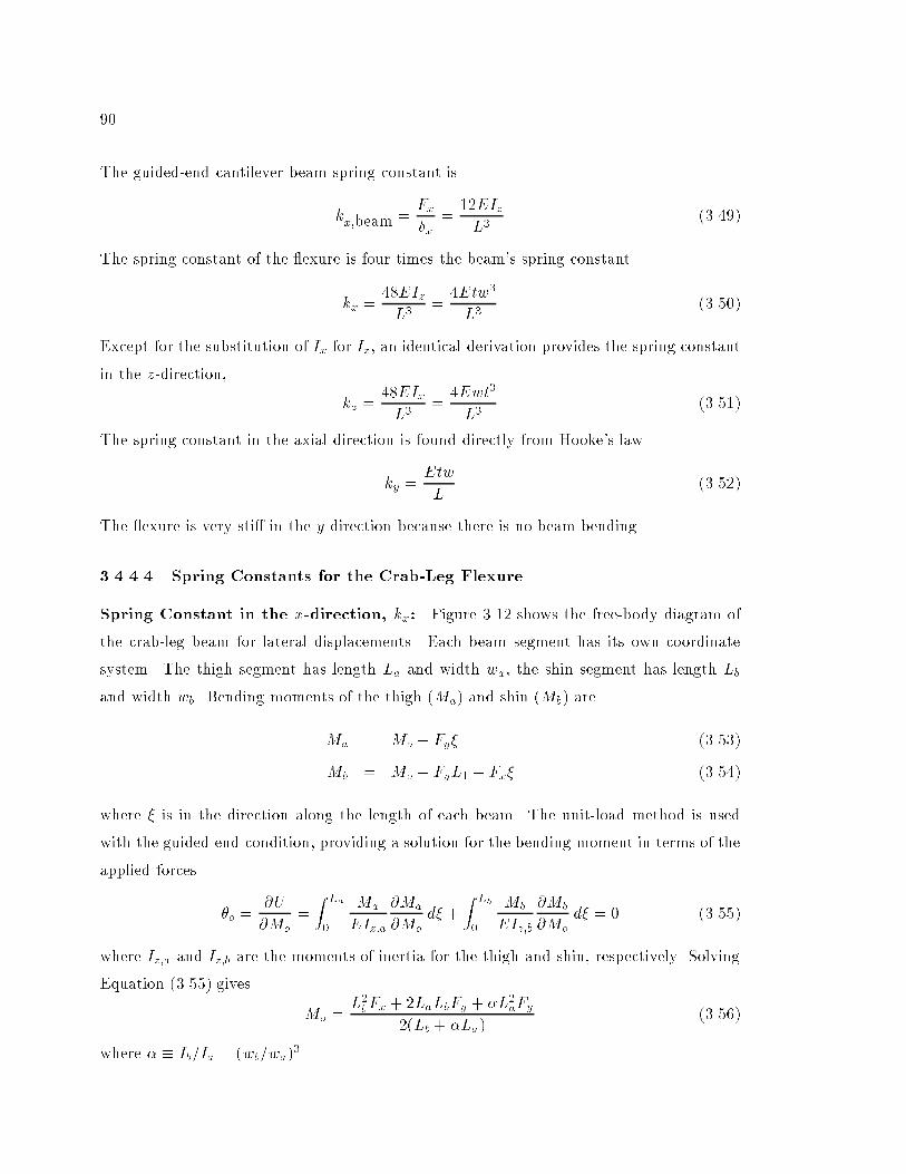
Measured lateral resonant frequency values are given in Table 3.4. Finite-element
resonant frequency values are within 13 % of the average measured values for all resonators
except for the A resonator. An estimation of resonant frequency, tabulated in the last
column of Table 3.4, is calculated using
fr =1
2
skxm
(3.144)
where m is the shuttle mass and kx is taken from Table 3.2. These analytic resonant
frequency values are 1030% larger than the nite-element values because the eect of
spring mass on resonant frequency is neglected. More accurate expressions for resonant
frequency can be determined by substituting an eective mass for m in Equation (3.144)
to account for inertial eects of the springs. Neglecting the spring mass is a particularly
114
label measured fr nite analytic fr =left center bottom avg std dev element fr
pkx=m=2
[Hz] [Hz] [Hz] [Hz] [Hz] [Hz] [Hz]
A 2810 2485 2795 2697 183 3032 3866
B 3230 3165 3120 3172 55 3137 3920
C 7870 7180 7595 7548 347 7376 8614
D 8430 7760 8210 8133 342 7635 8791
E 4260 2770 3015 3348 799 2899 3887
F 3095 2780 2980 2952 159 2947 3843
G 7520 6800 7320 7213 372 7053 8546
H 7625 6905 7445 7325 375 7243 8589
I 18395 16910 18305 17870 833 17029 18780
L 18290 16935 18055 17760 724 17130 19058
Table 3.4: Measured lateral resonant frequency of serpentine microresonators.
bad approximation for resonators A, B, E, and F, where the total spring length is greater
than 0.5 mm. Residual stress in the lm has less than 1 % eect on the spring constants
or resonant frequency of these structures, based on nite-element simulations. Accurate
measurement of spring constants can be done using a static force versus displacement test,
or using a resonant frequency test with models that include the eects of spring mass.

115
+q −q
−−−
−−+
+++
+
V+ −
x
FeFe
Figure 3.24: Schematic of two charged conductors, where V is the voltage between theconductors, q is the amount of dierential charge on each conductor, x is the relativedisplacement, and Fe is the electrostatic force acting on the conductors.
3.5 Electrostatic Actuators
3.5.1 Electrostatic Force
Electrostatic force between two charged conductors, shown in Figure 3.24, can be
determined from conservation of power of the system [75]:
d
dtWe(q; x)| z
rate of change of
stored energy
= Vdq
dt| z electric
power
Fe
dx
dt| z mechanical
work
(3.145)
where We(q; x) is the stored electrical energy, V is the voltage between the conductors, q
is the amount of dierential charge on each conductor, x is the relative displacement, and
Fe is the electrostatic force acting on the conductors. Multiplying Equation (3.145) by dt
gives the dierential energy-balance relation11,
dWe = V dq Fedx (3.147)
11For a general system of n + 1 conductors (one of the conductors is the ground reference) and p forces,the dierential energy balance is
dWe =
nXi=1
Vi dqi
pXj=1
Fe;jdxj (3.146)
where Vi and qi are the respective voltages and charges associated with the ith conductor, and Fe;j, and xjare the respective generalized forces and relative displacements associated with the jth conductor.

116
V’
V
F =0e
W’e
x x’
q(x,V’)
(x,V)
Figure 3.25: Path of integration in the x-V variable space used to calculate coenergy.
Balance of energy can be alternatively expressed in terms of V and x as the independent
variables, by
dW 0
e = q dV + Fedx (3.148)
where the coenergy, W 0
e(V; x), is dened as
W 0
e = q V We (3.149)
We can integrate Equation (3.148) along an arbitrary path in the variable space xV ; we
choose the path shown in Figure 3.25 to nd the coenergy,
W 0
e =Z x
0Fe(x
0; V = 0) dx0| z = 0
+Z V
0q(x; V 0) dV 0
=Z V
0C(x)V 0 dV 0 =
1
2C(x)V 2 (3.150)
where C(x) is the capacitance between the conductors12. Our choice of integrating over x
with V xed at zero has simplied the evaluation by eliminating the rst term in Equa-
tion (3.150).
The electrostatic force is found by taking the partial derivative with respect to x
in Equation (3.148). After rearranging terms, we nd
Fe =@W 0
e
@x q
@V
@x| z = 0
(3.151)
12The chargevoltage relationship is linear for a pair of conductors in air. Therefore, q = C V , where C isthe capacitance.

117
(a)
(b)
Si substrate
substrate electrode
zo
x
y z
z
y x
A
A’A
A’suspendedmovable structure
x
L
Figure 3.26: Parallel-plate microactuator. (a) Top view. (b) Side view.
where the second term is zero because V is constant. Substituting Equation (3.150)
into (3.151), we obtain
Fe =1
2
dC(x)
dxV 2 (3.152)
Equation (3.152) can be used to calculate the electrostatic force of any two-conductor sys-
tem, given the capacitance as a function of position. We will revisit the energy-method
derivation of electrostatic force for a system with three conductors in section 3.5.3.
3.5.2 Parallel-Plate Actuators
The parallel-plate microactuator, shown schematically in Figure 3.26, produces
electrostatic force in the x and z directions. The parallel-plate area has a xed dimension,
L, and a variable dimension, x. Neglecting fringing elds, the parallel-plate capacitance is
C =o Lx
z(3.153)

118
where o is the permittivity of air13, and z is the vertical air-gap spacing. Application of
Equation (3.152) gives the forces that act on the movable plate.
Fe;x =o L
2 zV 2 (3.154)
Fe;z = o Lx
2 z2V 2 (3.155)
A second-order correction to Equation (3.155) includes the eect of fringing ca-
pacitance from the edge of the movable plate to the lower electrode, and has been used
to model electrostatically deformed beams and diaphragms [76]. Analytic approximations
to parallel-plate edge-fringe capacitance can be found in texts on microstrip transmission
lines [7779]. Plates that are perforated with holes will have a smaller capacitance than that
of a solid plate. The edge-fringe and hole-fringe capacitances change with vertical position,
and, therefore, aect the value of electrostatic force.
We have used two-dimensional nite-element analysis to model specic parallel-
plate-capacitor geometries. In system-level simulations, we use the following approximate
relation for vertical parallel-plate electrostatic force:
Fe;z '
1 (z=zo)2V 2 (3.156)
where is a form factor that includes the fringe-eld eects, and z is a vertical displace-
ment about the nominal air gap, zo.
3.5.3 Comb-Finger Actuators
The comb-nger microactuator (comb-drive), shown schematically in Figure 3.27,
was rst used by Tang [20] in a laterally driven polysilicon resonator. Two sets of engaged
comb ngers, one movable set (rotor) and one stationary set (stator), are patterned from a
single polysilicon lm. A ground plane is located under the comb ngers, and is normally
electrically connected to the rotor to eliminate electrostatic pull-down force to the substrate.
We will use the subscripts s, r, and p to denote variables relating to the stator ngers, rotor
ngers, and underlying plane, respectively.
3.5.3.1 Comb-Drive Lateral Force
In Figure 3.28, a comb-nger cross section illustrates the partitioning of capac-
itance per unit length into the stator-to-rotor capacitance, Crs, the rotor-to-plane capac-
13The permittivity of air is approximately equal to that of a vacuum, 8.854 1012 F/m.

119
x
y z
z
y x
A A’
A A’
Si substrate
stationary, stator fingers (s)
movable, rotor fingers (r)
ground plane (p)
Figure 3.27: Electrostatic comb drive (a) Top view. (b) Side view.
itance, Crp, and the stator-to-plane capacitance, Csp14. Extension of the analysis of sec-
tion 3.5.1 to three conductors yields the dierential coenergy of the comb-drive,
dW 0
e = qsdVs + qrdVr + fe;xdx (3.157)
where fe;x is the x-directed force per unit length. We integrate Equation (3.157) along the
path shown in Figure 3.29 and obtain
W 0
e =
Z x
0fe(x
0; Vs = 0; Vr = 0) dx0| z = 0
+ (3.158)
Z Vs
0qs(x; V
0
s ; Vr = 0) dV 0
s +
Z Vr
0qr(x; Vs; V
0
r) dV0
r
=1
2Csp(x)V
2s +
1
2Crp(x)V
2r +
1
2Crs(x) (Vs Vr)
2 (3.159)
where charges per unit length associated with the stator and rotor ngers are
qs = (Csp + Crs)Vs CrsVr (3.160)
qr = CrsVs + (Crp + Crs)Vr (3.161)
We apply Equation (3.151) to get the comb-drive electrostatic force,
14In the two-dimensional analysis, the coenergy, charge, and capacitance are expressed per unit length ofthe comb nger. We use the symbol C for capacitance per unit length, and fe for force per unit length.We retain the symbols for charge (q) and coenergy (We) when discussing per-unit-length quantities; whichdenition is used will be apparent in the context.

120
ground plane (p)
rotor (r)
stator (s)
z Crs1
2 Crs1
2
Csp1
2Crp−
+Vs
+
−Csp
1
2Vr
Figure 3.28: Cross-section of one rotor nger between two stator ngers, showing the par-titioning of capacitance for comb-drive force evaluation.
F =0e
Vs
V’s
x’x
Vr
V’r W’e Vs ,Vr )(x,
Vs ,qr rV’ )(x,
,qs(x, rV =0)sV’
Figure 3.29: Path of integration in the x-Vs-Vr variable space used to calculate the comb-drive coenergy.

121
(b) (c)
ground plane
statorstator
−
+VsC
1
2 sp,uC1
2 sp,u
x
y z
L
L
x
z
xy
region 2
region 1
region 3
(a)
rotor
stator
ground plane
rotor statorstatorCrs
1
2 Crs1
2
Crp−
+Vs
+
−C
1
2 sp,e C1
2 sp,erV
Figure 3.30: Comb-drive schematics for evaluation of lateral force. (a) Comb-drive layout,showing the three comb-nger regions: 1. unengaged rotor ngers, 2. engaged ngers, and3. unengaged stator ngers. (b) Cross section of engaged comb ngers. (c) Cross section ofunengaged stator ngers.
Fe;x =1
2
dCsp
dxV 2
s +1
2
dCrp
dxV 2
r +1
2
dCrs
dx(Vs Vr)
2 (3.162)
where we have switched from per-unit-length capacitances to total capacitances. When the
ground plane is electrically connected to the rotor (Vr = 0), Equation (3.162) reduces to
Fe;x =1
2
d
dx(Csp + Crs)V
2
s (3.163)
To nd the total change in comb-nger capacitances with x, we can evaluate comb-
drive cross sections where the ngers are engaged and unengaged, as shown in Figure 3.30.
Since we assume that Vr = 0, there is no energy storage in region 1 (unengaged rotor ngers
in Figure 3.30(a)) and we can ignore its capacitance contribution. Region 2 (engaged ngers)
and region 3 (unengaged stator ngers) correspond to the cross sections in Figures 3.30(b)
and (c), respectively. Then, the total rotor-to-stator and stator-to-plane capacitances are
Crs = N Crsx (3.164)
Csp = N [Csp;ex+ Csp;u(L x)] (3.165)

122
where N is the number of rotor comb ngers15, L is the comb-nger length, x is the
nger overlap, and Csp;e and Csp;u are the capacitances per unit length of the engaged and
unengaged ngers, respectively. Using Equation (3.163), we nd the lateral comb-nger
force,
Fe;x =N
2(Crs + Csp;e Csp;u)V
2
s (3.166)
The lateral force is independent of the x position, if three-dimensional fringe elds are
neglected. In system-level simulations, we express the lateral comb-drive force in terms of
the parallel-plate, rotor-to-stator nger capacitance ( = 2oNt=g), giving
Fe;x = oN t
gV 2 (3.167)
where t is the comb nger thickness, g is the gap between the comb ngers, and is a form
factor that includes the fringe-eld eects.
Plots of the capacitances and lateral force versus vertical displacement of the rotor
comb ngers are given in Figure 3.31(b), for the comb-drive geometry in Figure 3.31(a).
Values are generated with the MaxwellTM electrostatic nite-element software [52]. For
z = 0, the lateral force is 10.1 pN/V2/nger, corresponding to a form factor ( in
Equation (3.167)) of 1.14. The force varies with the rotor's vertical displacement, hav-
ing a maximum value at around z = +1 m. The stator-to-plane capacitance terms
in Equation (3.166) (Csp;e and Csp;u) were not included in an initial analysis of the comb
drive [54]. Neglecting these terms results in a 2045 % overestimate16 of the lateral force
since Csp;u > Csp;e.
3.5.3.2 Comb-Drive Levitation Force
The relation for comb-drive levitation (z-directed) force is analogous to Equa-
tion (3.162) for lateral force, and given by
Fe;z =1
2
dCsp
dzV 2
s +1
2
dCrp
dzV 2
r +1
2
dCrs
dz(Vs Vr)
2 (3.168)
If we neglect fringing elds and assume Vr = 0, the vertical force relation reduces to
Fe;z =1
2N x
d
dz(Csp + Crs)V
2
s (3.169)
15We assume that the capacitance at the outside edge of the rst and last stator comb ngers does notchange with x and can be ignored.
16For z = 0, the calculation of lateral force using fe;x = 0:5CrsV2 gives 14.6 pN/V2/nger, which is a
44 % overestimate of the actual value.

123
−1.5
Force
−1 0 1 2
Crs
Vertical displacement of rotor, m]µz[∆(b)
(a)
ground plane
rotorstatorstator
z
xyzo
t g
w
z∆
zow = t = g = mµ= 2
0
5
10
15
20
25
30
Cap
acita
nce
[pF
/m]
35
40
45
50
0
5
10
15
20
25
30
35
40
45
50
[pN
/V2
Late
ral f
orce
/fing
er]Crp
0.5 1.5−0.5
Csp,u
Csp,e
Crs + Csp,e
Figure 3.31: Finite-element calculations of capacitance and lateral force for a common comb-drive geometry. (a) Cross section of comb-nger geometry with w = t = g = zo = 2 m.(w is the nger width, and zo is the stator nger spacing above the substrate.) (b) Plots ofcapacitance and lateral force versus the rotor's vertical displacement, z.

124
−1.5−1.0
−0.50.0
0.51.0
1.52.0
2.53.0
3.5
−1 0 1 2
2Le
vita
tion
forc
e[u
N/m
/V/fi
nger
]
Vertical displacement of rotor, m]µz[∆
∆ze
Figure 3.32: Plot of vertical force, fe;z , versus the rotor's vertical displacement, z, for thecomb-drive geometry of Figure 3.31(a), where w = t = g = zo = 2 m.
where Csp and Crs are independent of lateral position.
In Figure 3.32, the levitation force is plotted as a function of the rotor's vertical
displacement for the comb-drive geometry of Figure 3.31(a). Again, values are calculated
using the Maxwell nite-element analysis software. The force is proportional to the slope
of the Csp + Crs curve in Figure 3.31(b) and is positive for displacements less than z =
ze 1 m. Since the force is approximately linear with displacement, it can be modeled
with an electrical spring constant, ke, by the relation [80]
Fe;z = ke (ze z) (3.170)
For the comb-drive geometry in Figure 3.31(a), ke corresponds to about 1.7 N/m2/V2
per comb nger. If the rotor suspension has spring constant kz , then the equilibrium
displacement is
z =ke
kz + keze (3.171)
At this displacement, the electrostatic levitation force equals the spring's restoring force.

125
z
Aarea,
uppermovableplate
crab−legbeam
C
Cpp
Cpu
C
B B’
B’B
substrate
oxide
Cf1 f2
lower plateanchorplane
(a)
(b)
pl
Figure 3.33: Schematic views of a micromechanical parallel-plate capacitor. (a) Top view.(b) Side view.
3.6 Capacitive Position Sensing
Sensing the position of a micromechanical structure is a key part of many micro-
systems. For polysilicon surface microsystems, capacitive sensing is a robust method of
determining position, having low sensitivity to temperature and stress. A limitless number
of capacitor geometries can be formed with surface-micromachined structures, however, we
will concentrate on the parallel-plate arrangement commonly used to detect vertical dis-
placement of a movable plate. Most of the concepts outlined here are applicable to other
micromechanical capacitors.
A movable air-gap capacitor is shown schematically in Figure 3.33. Four crab-leg
beams suspend the movable plate above a lower electrode by a distance, z. The sensor
capacitance has a parallel-plate component and fringing components given by
Cs =oA
z+ Cf1 + Cf2 (3.172)
where A is the lower electrode area. Contributions to the fringing capacitance come from
electric elds between the upper and lower plates (Cf1) and from elds between the lower

126
Cpp
substrate
lower plate
Cpl
upper plate
Cf1
Cpu
Cf2
Figure 3.34: Equivalent circuit of the micromechanical capacitor.
plate and anchor plane (Cf2). The sensor capacitance varies nonlinearly with position,
and the sensitivity, dC=dz, varies as 1/z2, approximately. Nonlinearity is a drawback for
position control, but does not aect closed-loop sensors where the position is nulled17.
Other, parasitic capacitance exists between each plate to the substrate, which is
assumed to be an ac ground. Both the lower plate parasitic capacitance, Cpl, and the
upper-plate parasitic capacitance, Cpu, can be much larger than the sensor capacitance,
because the oxide dielectric constant is higher than air and the oxide thickness is typically
smaller than the air gap. If a depletion capacitance to the substrate is present, then Cpl is
a function of the lower plate voltage.
The equivalent circuit for the capacitive element is given in Figure 3.34. Capaci-
tance associated with the air gap is variable, but the fringe capacitance to the anchor plane
is approximated as constant.
We will discuss two approaches to measurement of the sensor capacitance (and,
hence, vertical position): voltage sensing using a unity-gain buer and current sensing using
a transresistance amplier. Another important capacitance sensing method using charge-
redistribution sense techniques has been developed in a pressure sensor [81,82].
3.6.1 Capacitive Position Sensing Using a Unity-Gain Buer
One way to measure capacitance involves driving voltage on one node of the ca-
pacitor and sensing voltage on the other node. We will rst describe a sensor made from a
single micromechanical capacitor, then improve the circuit by connecting another capacitor
to form a voltage divider. Then, we analyze the unity-gain buer circuit used in our sensors.
17However, capacitive sensing produces a nonlinear vertical force that can aect sensor stability. Eectsof feedback-force nonlinearity are discussed in section 5.5.4.

127
Cpu
substrate
lower plate
Cpl
upper plate
Cs
+
−
mV
sV
= 1Go
Figure 3.35: Capacitive divider circuit using a single micromechanical capacitor.
Last, experimental results for the buer are presented.
3.6.1.1 Single-Capacitor Sensor
The micromechanical sense capacitor in Figure 3.33 forms an ac voltage divider
when one plate is driven by an ac voltage source. In the circuit of Figure 3.35, the upper
plate is connected to the ac modulation source, Vm, and the lower plate becomes the high-
impedance divider output node. A unity-gain buer senses the voltage on the lower plate,
providing a low-impedance output, Vs, where
Vs = GoVm
Cs
Cs + Cpl
!(3.173)
where the buer gain, Go, is 1 nominally. Since the upper plate is a low-impedance node,
the upper-plate parasitic capacitance to ground has no eect on the circuit. The roles of
the plates can be switched, with the lower plate driven; such upper-plate sensing has been
used in a surface-micromachined accelerometer [64]. Then, the upper-plate capacitance to
ground replaces Cpl in the denominator of Equation (3.173). The dc bias for the high-
impedance node can be set with a large resistor or a back-biased diode that leaks charge to
ground.
For small-signal calculations, it is convenient to separate the sense capacitance
into a xed part, Csf , and a variable part, Csv , instead of using a parallel-plate and fringe
decomposition.
Cs = Csf + Csv = Csf +Csvo
1 +z=zo(3.174)
where a small displacement around an operating point is dened such that z = zo+z. For
simplicity, we assume that the all of the fringing capacitance is xed, so Csvo=oA=zo Sub-
stitution of Equation (3.174) into Equation (3.173) leads to the linearized relation between
128
displacement and sensor output voltage.
Vs = GoVmCso
Cso + Cp
"1 +
Csf
Cso
Csf + Cp
Cso + Cp
!z
zo
#(3.175)
where Cso = Csjz=0 = Csf + Csvo, and Cp is the parasitic capacitance from the high-
impedance node to ground (Cp=Cpl, for the present conguration). The sensor gauge factor,
@Vs=@z, approaches zero in the limit of very small or very large parasitic capacitance, and
is maximized when Cp=Csvo.
There are two objections to using this single air-gap capacitor as a position sensor.
First, the parasitic capacitance can be relatively large, yielding unacceptably low sensitivity.
If the lower electrode is the high-impedance node, the parasitic capacitance is typically
around 16 times the sensor capacitance, assuming a 2 m air-gap and 5000 A of oxide under
the lower plate. Thicker oxide lms can be used, but this solution may cause processing
problems. If the upper plate is used as the high-impedance node, the anchors represent
a large parasitic capacitance (Cpu in Figure 3.33). Interconnect from the capacitor to
the buer also adds to the parasitic capacitance. The second objection to single air-gap
capacitive sensors is the large, common-mode component of the sensor gain. In order to
amplify the displacement signal, the common-mode component must rst be subtracted
from the overall output.
3.6.1.2 Balanced Capacitive Divider With Driven Shield
Parasitic capacitance to ground can be greatly reduced by incorporating an extra
shield electrode around the high-impedance node, as shown in the cross-section of Fig-
ure 3.3618. An extra layer of polysilicon is located under the lower sensor plate, shielding
electric eld lines from the substrate. If the buer drives the shield at the same potential as
the high-impedance node, then the eective parasitic capacitance is reduced to nearly zero.
An improved position detector circuit, including the shield, is shown in Figure 3.37.
The lower plates of two air-gap capacitors are connected to form a voltage divider. One of
the capacitors has a clamped upper plate and serves as a reference, with a xed air-gap. In
some applications [64], fully-dierential capacitive bridges can be made; however, we will
restrict our discussion to the divider circuit with a xed reference capacitor. The two ac
18For simplicity, we schematically represent the variable (Csv) and xed (Csf) components of the sensorcapacitance as lumped elements in Figure 3.36.

129
z
C
C
Cpu
C
substrate
oxide
lower plate
anchorplane
driven shield
Cg
sfsv
pl
Figure 3.36: Schematic cross-section of a micromechanical parallel-plate sense capacitorwith a driven shield. The sense capacitor is connected in series with an identically sizedreference capacitor (not shown) to form a capacitive voltage divider.
+
Cpu
C
Cs−
mVsV
Cpu
substrate
C
CmV
+
−
+
−r
g
p
sense upper plate
reference upper plate
lower plates
shield
= 1GoVin
Figure 3.37: Balanced capacitive divider circuit.

130
modulation voltages that drive the upper plates are generated by sine-wave or square-wave
sources that are 180 out of phase with each other.
Parasitic capacitance directly to ground is eliminated, because the shield termi-
nates electric elds from the lower plates. The buer circuit drives the voltage across Cp to
nearly zero, with the resulting eective capacitance to ground19 given by
C0
p = (1Go)Cp (3.176)
and the sensor output voltage is
Vs = GoVm
Cr Cs
Cr + Cs + C0
p
!(3.177)
By substituting Equation (3.174) into Equation (3.177), the relation between sensor output
and displacement is derived.
Vs = GoVm
Cr Cso
Cr + Cso + C0
p
!266641 +
Cr Csf
Cr Cso
zzo
1 +
Cr + Csf + C0
p
Cr + Cso + C0
p
zzo
37775 (3.178)
If the sense and reference capacitors are matched (Cr=Cso), Equation (3.178)
reduces to
Vs = GoVm
Csvo
Cr + Cso + C0
p
!26664 z=zo
1 +
Cr + Csf + C0
p
Cr + Cso + C0
p
zzo
37775 GoVm
Csvo
Cr + Cso + C0
p
!z
zo
(3.179)
Notice that the drawbacks associated with the single-capacitor sensor are remedied with
the shielded, matched-capacitor divider. The sensitivity is not impacted by the parasitic
capacitance, as long as C0
pCso. The xed term of Equation (3.175) has no counterpart in
Equation (3.179); the balanced modulation combined with the matched divider cancels out
the common-mode components.
3.6.1.3 Unity-Gain Buer
Buer Description
19Any parasitic capacitance that cannot be shielded, such as buer input capacitance, is added directlyto C 0
p to give the total eective parasitic capacitance to ground.

131
M1 M2
M3 M4100
4100
4
1004
2 X100
42 X
1004
2 X
Vdd
Vss
= 4.0 V
1004
2 X
= −2.5 V
(external)20kΩ
M5 M6
M7M8
42 X
50
M9
42 X
50
Voff−chip
µ80 AIB=CL
M10
1008
1008
D1Vin
+
−
Vout
+
−
+
−
Vss
Vdd
Figure 3.38: CMOS unity-gain buer circuit.
The capacitive sense circuits described above require a buer with gain close to
unity for eective shielding of the parasitic capacitance to ground. We use the CMOS
unity-gain buer circuit, shown in Figure 3.38, which is an improved version of a previous
design [83, 64]. Gate width to length ratios (W=L) are given next to each transistor, with
paralleled (2) transistors noted. The single-stage design has a moderate open-loop voltage
gain, but is stable even when driving large capacitive loads. Unity-gain feedback is achieved
by connecting the output node (M2 drain) to the negative input node (M2 gate) of the
dierential pair. The diode, D1, sets the input dc bias to ground, and a 20 k external
resistor supplies bias current for the circuit. Load current in each branch is matched with
the p-channel current mirror (M5M6). The dierential stage drives a substantial on-chip
load capacitance, CL, which comes from the interconnect and shield, while a source follower
(M9M10) drives the even larger, o-chip capacitance.

132
For micromechanical capacitive sensing applications, a key design issue is mini-
mization of buer input capacitance, which adds directly to parasitic capacitance on the
high-impedance node and decreases the output sensitivity. The requirement of a reason-
able open-loop gain value dictates that the input transistor size cannot be made arbitrarily
small. There are three contributors to capacitance at the gate of M1: gate-to-source capac-
itance (Cgs), gate-to-drain capacitance (Cgd), and gate-to-body capacitance (Cgb). Buer
input capacitance can be reduced by forcing the source, drain, and body voltages to track
the gate voltage. The small-signal gate-to-source voltage of M1 is approximately inversely
proportional to the open-loop voltage gain of the dierential stage, providing the desired
reduction in the Cgs component of input capacitance. Since a p-well CMOS process is used,
we can connect the input transistor well and source together, thereby reducing the eect of
Cgb on input capacitance. Transistors M3 and M4 are included to mirror the output voltage
to the drain of M1. Thus, because the drain and gate voltage track, the eect of Cgd on
input capacitance is reduced. In our analysis, both Cgb and Cgd can be added to the ca-
pacitance to ground, Cp; however, the addition should not be necessary, since interconnect
capacitance will be the dominant component of the parasitic capacitance.
Buer Circuit Analysis
Using the low-frequency, small-signal equivalent circuit shown in Figure 3.39, we
can determine the buer performance specications: gain transfer function (G(s)), input
impedance (Zi(s)), output resistance (Ro), and bandwidth (fo). The resulting equations
are
G(s) =
1 +
1
gm;M1ro;M6
+sCL
gm;M1
!1
(3.180)
Zi(s) =
"sCgs;M1
2gm;M1
1
ro;M7
+1
ro;M6
+ sCL
!#1
(3.181)
Ro =1
gm;M1
(3.182)
fo =gm;M1
2CL(3.183)
where gm is the transconductance and ro is the output resistance of a transistor. Only rst-
order eects are included, where the gain of each transistor is assumed to be much greater
than one. We have also assumed that Cgs is much larger than Cgd and Cgb. The input
impedance is capacitive at lower frequencies, and has a resistive component that becomes

133
1/gm,M5
1/gm,M2
1/gm,M4
+
−
o,M3rv3
v3gm,M3
+
v6ro,M6
−
v6gm,M6
ro,M7
gm,M1v1 ro,M1
+
−
v1
+
−
vi
+
−
vo
LC
Figure 3.39: Low-frequency, small-signal model of buer circuit.

134
dominant above 230 kHz. Compared to the previous buer design (which omitted M5 and
tied the drain of M3 to Vdd), the dc gain error is reduced by a factor of 4, and the input
capacitance is reduced by a factor of 2.
Further improvement of the gain can be made by using a cascode p-channel current
mirror in place of the M5M6 mirror. Notice that the output resistance of the n-channel
mirror, M7M8, does not aect the gain. Input capacitance can be reduced by increas-
ing the output resistance of both n- and p-channel current mirrors. The resistive input
impedance can be reduced by minimizing load capacitance. The input gate length should
be of minimum size, since input capacitance (Ci) scales as20 L3=2W 1=2.
Values for Buer Specications
To obtain values for the buer specications, we must rst dene the MOS eld-
eect-transistor (FET) parameters, then calculate values of transconductance and output
resistance for the buer-circuit transistors. MOSFET drain current, transconductance,
output resistance, and gate-to-source capacitance in the saturation region are given by [84]
Id =k0
2
W
L(Vgs Vt)
2(1 + Vds) (3.184)
gm =q2k0Id(W=L) (3.185)
ro =1
Id(3.186)
Cgs =2
3CoxWL (3.187)
where Vt is the threshold voltage, Cox is the gate oxide capacitance per unit area, k0 is the
intrinsic transconductance factor21 and is the channel length modulation factor. These
are all treated as constant parameters, dependent on the fabrication process. The body
and source are connected for all transistors in the circuit, so there is no body eect on the
threshold voltage. Parameters for our 3-m p-well CMOS technology are, for n-channel
devices:
k0n = 33A/V2
n = 0:043 V1
Vtn = 0:56 V
20The input capacitance, Ci, is proportional to Cgs=(gmro), where gm ro, and Cgs are given by Equa-tions (3.185) through (3.187). Therefore, Ci / CoxIdL
p2k0
nIdW L.21In theory, k0 = Cox, where is the carrier mobility. In practice, k0 is determined experimentally from
transistor IV measurements.

135
Cox = 0:69 fF/m2
Ld = 0:22 m
and for p-channel devices:
k0p = 17A/V2
p = 0:023 V1 (L = 8 m)
Vtp = 0:56 V
Cox = 0:69 fF/m2
Ld = 0:16 m
where Ld is the source/drain lateral diusion distance. These process parameters are used
in Equations (3.185)(3.187) to obtain values for selected device parameters.
gm;M1 = 0:385 mS
ro;M6 = 1:09 M
ro;M7 = 291 k
Cgs;M1 = 552 fF
Cgo;M1 = 150 fF
The last parameter is the total overlap capacitance, Cgo, between the gate to the source,
drain, and substrate, which is specied as a process parameter. We add the overlap ca-
pacitance directly to Cgs when calculating the input capacitance of the buer. The buer
specications are calculated from Equations (3.180)(3.183). We assume a load capaci-
tance of 3 pF, re ecting the size of the shield-to-ground capacitance in our experimental
test structures. Table 3.5 lists the analytical values of buer specications alongside values
determined using the HSPICE [3] simulation program. The HSPICE simulations use the
specication symbol analytic HSPICE
dc gain Go 0.991 A/V 0.9965 A/V
input capacitance Ci 3.97 fF 4.32 fF
output resistance Ro 2.60 k 2.80 k
bandwidth fo 20.4 MHz 20.2 MHz
Table 3.5: Values of buer performance specications, calculated from analytic analysis andHSPICE [3] simulation.
input deck in appendix B.1. Source/drain junction and overlap capacitance are included in
the transistor models. Analytic and simulated results are in reasonable agreement.

136
Diode Capacitance
The input diode has junction capacitance to ground that must be included in the
total input capacitance. Assuming a step junction, capacitance per unit area of the p-n
diode is given by [68]
Cj =
24 qs
2
1Na
+ 1Nd
(i Va)
351
(3.188)
where the terms in the equation are
electronic charge: q = 1:602 1019 C
permittivity of silicon: s = 1:04 1010 F/m
acceptor (p-type) dopant concentration: Na = 2 1016 cm3
donor (n-type) dopant concentration: Nd = 2 1018 cm3
built-in junction voltage: i = 0.6 V
forward bias voltage across diode: Va = 0 V
Diode D1 has an n+ diusion area of 135 m2. Plugging numbers into Equation (3.188), we
arrive at a diode capacitance value of 71 fF, much larger than the buer input capacitance
value of 3 fF.
When the diode is exposed to light, minority carriers are generated, producing
a reverse current. This photocurrent is balanced in steady-state by a forward bias across
the junction. Equation (3.188) is only valid for forward-bias voltages up to about 0.3 V.
For greater forward-bias voltages up to about 0.6 V, the junction capacitance increases
to about 23 its zero-bias value, but remains nite [85]. Future designs should consider
other means of dc biasing the buer, since the diode junction capacitance dominates the
eective parasitic capacitance to ground. An undoped polysilicon resistor or a long-channel
transistor may provide a high-resistance dc path to ground with lower capacitance than the
diode.
Buer Noise
MOS transistor noise is modeled by an equivalent, input-referred voltage source
with thermal noise and icker noise (1/f noise) components [84].
v2eq = 4kBT
2
3gm
f +
Kf
CoxWLff (3.189)
where kB is Boltzmann's constant, T is temperature, Kf is the icker noise coecient, and
f is a small bandwidth. v2eq denotes the mean-square of the equivalent noise distribution.

137
Csensor
M1 M2
M3 M4100
4100
4
1004
2 X100
42 X
Vdd
Vss
M5 M6
IB
1008
1008
D1 Vout
+
−
v2eq1 v2
eq2
v2eq5 v2
eq6
2id1
−
Vin
+
Figure 3.40: Noise model of buer circuit.
Shot noise and icker noise are present in pn diodes, which are modeled by an equivalent
current source, i2d.
i2d = 2qIdf +KdIdff (3.190)
where q is the electronic charge, Id is the diode current, and Kd is the icker noise coecient
for the diode.
Buer input-referred noise is determined using the equivalent circuit shown in
Figure 3.40. Noise contributions come from transistors M1, M2, M5, and M6, and diode
D1. The bias-current transistors (M7 and M8) only aect the common-mode current, and
transistors M3 and M4 are cascoded, so none of these devices add to the output noise.
Noise from the source-follower stage will be ignored, but extra thermal noise is contributed
from transistors M8, M9, and M10. Interconnect thermal noise will be ignored for now, but

138
will be reconsidered when calculating the minimum detectable displacement of the position
sensor, in section 3.6.3. The total equivalent input-referred noise voltage, v2b , is given by
v2b = v2eq1 + v2eq2 +
gm;M6
gm;M1
!2 v2eq5 + v2eq6
+ v2eq,d1 (3.191)
where v2eq,d1
is the equivalent noise voltage of the diode, discussed next.
In steady-state and assuming the circuit is in darkness, the dc diode current is
zero; however, an ac current of amplitude 2fCjVin ows across the diode junction. The
noise current can be expressed as an equivalent noise voltage, v2eq,d1, assuming the buer is
connected to the capacitive divider sensing circuit. This gives
v2eq,d1 =
2q +
Kd
f
Cj
2f(Cj + Ci + Csensor)2
qV 2in f (3.192)
where Csensor is the total eective sensor capacitance22, andqV 2in is the root-mean-square
(rms) buer input voltage. Notice that the diode shot noise current produces a 1/f depen-
dence in the input-referred noise voltage.
Substituting Equation (3.189) and (3.192) into Equation (3.191), we arrive at
v2b = 4kBT
4
3gm;M1
!0@1 +sk0p(W=L)M6
k0n(W=L)M1
1Af +
2Kp
Cox(WL)M1f
1 +
Kpk0
pL2M1
Knk0nL2M6
!f +
Cj
2f(Cj + Ci + Csensor)2
2q +
Kd
f
qV 2in f (3.194)
where Kn and Kp are the icker coecients for the n-channel and p-channel transistors,
respectively. The rst term in Equation (3.194) is from transistor thermal noise, the re-
maining terms are from icker and shot noise. We now plug the transistor parameter values
into Equation (3.194) and obtain
v2bf
= 7:7 1017V2 +1:3 107V/s
f
qV 2in +
1:3 104V/s2
f2
qV 2in (3.195)
where we have used typical values for the icker coecients, Kn=Kp=31024 V2-F and
Kd=31016A, and the total sensor capacitance is assumed to be 90 fF. A plot of the input-
referred noise voltage spectral density is shown in Figure 3.41 for a 0.1 mV-rms input signal.
For this level of input signal, the input-referred transistor icker noise and diode shot noise
22For the balanced capacitive divider,
Csensor = Cs + Cr +C 0
p (3.193)

139
frequency [Hz]
v2i
∆ f
10−12
10−14
10−16
100 10 k 1 M 100 M10 1 k 10 M100k10−17
10−15
10−13
10−11
−1010
thermalnoise
diode shot noiseand transistorflicker noise (1/f)
(1/f )2diode flickernoise
Figure 3.41: Typical buer noise voltage spectral density.
are approximately equal and are the dominant contributors to noise voltage between 470 Hz
and 350 kHz. Larger input signals, or the presence of diode photocurrent, will make the
shot noise dominate over the transistor noise. Below 470 Hz, the diode icker noise voltage
becomes the largest noise component, while thermal noise dominates above 350 kHz.
In position-sensing applications, the buer signal of interest may only span a lim-
ited bandwidth. Noise at frequencies outside of the signal band can then be ltered, thus
reducing the total noise voltage. As an example, we can calculate the equivalent noise volt-
age of the position-sensor circuit in Figure 3.37, using the CMOS unity-gain buer. The
balanced modulation driving the capacitor divider produces an amplitude-modulated out-
put signal. If we assume a modulation frequency of 100 kHz, a lter bandwidth of 50 kHz,
and an input signal level of 0.1 mV rms, the total noise is 4.6 V rms. The total noise rises
to 81 V rms when the input signal is increased to 100 mV rms. The diode noise is a large
portion of the total noise, providing more motivation (in addition to parasitic capacitance
reduction) to eliminate the diode from the buer circuit.
3.6.1.4 Buer Test Circuit
In order to test the balanced capacitive sensor and the unity-gain buer design, we
fabricated the test circuit shown schematically in Figure 3.42. The divider is made of eight
identical capacitors which can be disconnected from the circuit by cutting microbridge fuses.

140
V
VD1
Vin
shielded sensecapacitors
unshielded sensecapacitors
= 1Go
m−
m+
+
−
Vout
source−follower
+
−
Voff−chip
unity−gain buffer
fuses
#1 #5
#2 #6#3
#4
#7
#8
Figure 3.42: Schematic of the capacitive position-sense test circuit with a unity-gain buer.
Six capacitors have driven shields to reduce parasitic capacitance; the other two capacitors
do not have shields so we can experimentally compare sensing with and without shielding.
The completed test circuit is shown in Figure 3.43. The eight square, parallel-
plate capacitors, located above the circuitry in the micrograph, are 100 m on a side with a
2 m air gap, giving a capacitance value of 44 fF. The two unshielded capacitors have some
extra fringing capacitance, which increases their capacitance value to 47 fF. Each capacitor
is suspended by eight, 3-meander serpentine springs, which provide a sti support. The
springs are included to relieve any residual stress that might cause the upper plates to
buckle, and to allow verication that the plates are released by pushing them with a probe
tip. Tungsten interconnect from the capacitors to the buer is shielded using the underlying
gate-polysilicon layer. A shielded test pad is included to access the buer input. Other
bondpads are labeled for power, ground, bias current, modulation voltages, and outputs.
The pad labeled \OUT" is the on-chip buer output, and the \OUT+" pad is the o-chip
output. We had room on the chip to provide a large output driver, so the source-follower
transistors were increased in size to W=L=500/4.
A plot of the buer output voltages (Vout and Vo-chip) versus input voltage is
shown in Figure 3.44. Originally, we planned to use symmetric 2.5 V power supplies, but
the output saturated for input voltages above 0 V (dashed line). Instead, a larger Vdd value
of 4 V allows at least 0.5 V of input swing without degrading the output. The dc gain is
0.983, and the oset voltage is 3.9 mV. The source-follower dc gain is 0.994, and the o-chip

141
source−follower
#1
shielded sense capacitors unshielded sense capacitors
unity−gain buffer
Vin
diode
#2#3
#4#5
#6#7
#8
fuses
Figure 3.43: SEM of the capacitive position-sense test circuit with a unity-gain buer.

142
0.4
0.0
−0.4
−0.8
−1.2
−0.4 −0.2 0.0 0.2 0.4Vin [V]
Vout
Vout
Voff−chip
(Vdd = 2.5V)bu
ffer
outp
ut v
olta
ges
[V]
Figure 3.44: Plot of unity-gain buer output voltages versus input voltage.
# conguration Vppdescription [mV]
#0 no fuses cut +0:6
#1 #1 fuse cut +41:2
#2 #1,#2 fuses cut +0:3
#3 #1,#2,#3 fuses cut 65:6
#4 #1,#2,#3,#4 fuses cut 0:3
#5 #1,#2,#3,#4,#5 fuses cut +85:3
#6 #1,#2,#3,#4,#5,#6 fuses cut 0:6
Table 3.6: Description of each capacitive divider conguration and corresponding measuredpeak-to-peak output voltage, Vpp, for the waveforms in Figure 3.45.
signal has a dc oset of 0:81 V.
To verify operation of the sensor, we measured the buer output response to bal-
anced square-wave modulation across the divider. The modulation-voltage sources23, Vm+
and Vm, have a peak-to-peak amplitude of 0.606 V, as shown in Figure 3.45(a). Output
voltage waveforms are presented in Figure 3.45(b) for seven congurations of the capacitor
divider. A description of the divider congurations and the corresponding measured peak-
to-peak output voltages are given in Table 3.6. The fuse numbering (and corresponding
capacitor numbering) is dened in Figure 3.42. Fuses were cut in succession, starting with
23A circuit schematic of the modulation-voltage sources is given in appendix A.2.1.

143
0 5 10 15 20s]µtime [
mod
ulat
ion
volta
ges
[mV
]
0
−300
300Vm− Vm+
(a)
0 5 10 15 20s]µtime [
−180
−160
−140
−100
−120
buffe
r ou
tput
vol
tage
[mV
]
#0
#1
#3
#2,#4,#6
#5
(b)
Figure 3.45: Measured voltage waveforms from the position-sense test-circuit. (a) Modula-tion voltages. (b) Buer output voltage for seven dierent capacitor divider congurations.
fuse #1 and ending with fuse #6, and measurements were made after each cut. When the
divider is balanced (congurations #0, #2, #4, and #6), the peak-to-peak output is nearly
zero, re ecting the good matching of capacitance in the layout. There is more capacitance
in series with Vm+ than Vm for congurations #1 and #5, so the output voltage is in
phase with Vm+. In conguration #3, the divider weighting is reversed and the output
voltage is in phase with Vm. For the unbalanced cases, the peak-to-peak voltage increases
as fewer capacitors are left in the circuit, because the capacitance dierence becomes a
larger percentage of the total divider capacitance.
The output waveforms have a dc oset between 140 mV and 164 mV, arising
from ambient light generating a forward-bias across the diode. A darker ambient (room
lights o) results in dc osets between 0 V and 27 mV, which is in the range of the buer
oset. The asymmetric current-voltage diode characteristic is responsible for the positive
output dc-bias shift with increasing signal amplitude. The measured buer bandwidth is
about 2.8 MHz, corresponding to a 22 pF load that includes wiring to an external buer
amplier. This external buer amplier drives several feet of coaxial cable and is responsible
for the slower signal risetime of 1.3 s.
An expression for the eective parasitic capacitance in terms of known parameters
is obtained by inverting Equation (3.177).
C0
p =Go jVmj(Cr Cs)
jVsj Cr Cs (3.196)
where jVmj is the modulation amplitude, jVsj is the output amplitude, Cr is the capac-

144
itance in series with Vm+, and Cs is the capacitance in series with Vm. The parasitic
capacitance is separated into three components: eective parasitic capacitance associated
with a shielded capacitor, C0p(shielded), parasitic capacitance associated with an unshielded
capacitor, Cp(unshielded), and other parasitic capacitance associated with the diode and
interconnect, Cp(other). Using Equation (3.196) and the measured data in Table 3.6, we
extract the following values:
C0p(shielded) = 3 fF 1 fF
Cp(unshielded) = 197 fF 1 fF
Cp(other) = 172 fF 1 fF
Note the large reduction in eective parasitic capacitance due to the shield under the capac-
itors. The measured capacitance reduction corresponds to an approximate buer gain24 of
0.985, which is close to the measured buer gain (0.983). The substantial parasitic capaci-
tance associated with the diode and interconnect is mostly attributed to the diode junction
capacitance, since the interconnect is shielded. This capacitance falls within the predicted
range of values, and is about 2.5 times larger than the zero-bias junction capacitance value
of 71 fF.
3.6.2 Capacitive Position Sensing Using a Transresistance Amplier
3.6.2.1 Balanced Capacitive Divider
An alternate way to measure capacitance involves driving voltage across the ca-
pacitor and sensing the resulting displacement current. The same capacitive divider shown
in Figure 3.37 can be used with a transresistance amplier to sense the dierential dis-
placement current in the divider; the resulting schematic is shown in Figure 3.46. We have
swapped the connections of the sense and reference capacitors to reverse the sign of the
sensor output. The lower plates of the capacitive divider are forced to ground potential by
the operational amplier. A driven shield to reduce parasitic capacitance is unnecessary,
since the underlying substrate is an incremental ground.
24The buer gain is estimated from the shielded and unshielded parasitic capacitances by inverting Equa-tion (3.176)), giving Go = 1 C 0
p=Cp. However, because of dierences in the divider layout, the unshieldedplate's parasitic capacitance to ground is somewhat smaller than the shielded plate's capacitance to theshield. Considering the uncertainty in our measurement of the C 0
p(shielded), we can only make a roughcheck against the measured buer gain.

145
+
Cpu
−
mV sV
Cpu
substrate
mV
+
−
+
−
Cp
sense upper plate
reference upper plate
lower plates
+
−
Rf
transresistance amplifier
Cs
Cr
is
ir
iin
Figure 3.46: Balanced capacitive divider circuit with displacement current-sense using atransresistance amplier.
The displacement current, is, through the sense capacitor is given by
is =d
dt(CsVm) (Csvo + Csf )
dVmdt
+ Csvo
z
zo
dVmdt
+
CsvoVm
zo
dz
dt(3.197)
where we assume small displacements in the linear approximation. The rst term in Equa-
tion (3.197) is equal to the displacement current, ir, in the reference capacitor, with the
dierence between the currents given by
iin Csvo
z
zo
dVmdt
+
CsvoVm
zo
dz
dt(3.198)
This input current ows through the feedback resistor, Rf , and is converted to the output
voltage, where
Vs = Rf iin (3.199)
assuming an ideal operational amplier.
The balanced sinusoidal modulation voltage is
Vm = jVmj sin(2fmt) (3.200)
where jVmj and fm are the modulation amplitude and frequency, respectively. In contrast
to the voltage-sense method, a square-wave modulation source cannot be used, because
displacement current would only ow during the switching transient. The modulation fre-
quency must be at least twice the bandwidth of the displacement signal, to avoid aliasing at
the sensor output; however, fm is usually chosen to be much larger to ease the demodulation

146
lter requirements. In our analysis, we will assume that the modulation frequency is much
larger than the displacement signal bandwidth, so the second term in Equation (3.198) can
be neglected. Then,
iin Csvo
z
zo
dVmdt
(3.201)
A Laplace transform for the input current can be dened where the s parameter is a function
of the modulation frequency. Taking the transform of Equation (3.201), we obtain
Iin(s) ' sjVmjCsvo
z
zo
(3.202)
where s=j2fm.
The limited gain and bandwidth of the transresistance amplier produces a non-
ideal output response, which we will now explore. The output voltage Laplace transform is
given by
Vs(s) = sRf (Cs Cr)jVmj
1 +
1
Av(s)+
sRf (Cr + Cs + Cp)
Av(s)
1(3.203)
where Av(s) is the transform of the operational-amplier's open-loop gain. For large open-
loop gain, the small-signal output voltage transform is
Vs(s) ' sRfCsvojVmj
z
zo
(3.204)
We can increase feedback resistance or the modulation frequency and voltage to increase
the sensor gain. However, modulation voltage should be as small as possible to reduce
the eects of electrostatic force on the structure, modulation frequency is limited by the
bandwidth of the operational amplier, and feedback resistance is limited by available die
area. A reasonable set of values are jVmj=0.3 V, fm=1 MHz, Rf=200 k, Csvo=44 fF, and
zo=2 m, giving a sensitivity of 8.2 mV/m.
3.6.2.2 Transresistance Amplier
Circuit Description
We have implemented the transresistance amplier using a conventional two-stage
CMOS operational amplier. A circuit schematic of the transresistance amplier is shown
in Figure 3.47. The dierential input stage is followed by a common-source second stage.
A complementary source-follower output stage is used to drive the signal o-chip.

147
M2 M1
M3 M4
1004
1004
2004
2004
M5200
4
2004
M6
M10
2004
2004
2004
2004M7
M9
M8
M12
M11
2004
2004
Vdd= 4.0 V
Vss = −2.5 V
(external)20kΩ
µ80 AIB=
Vin
+
−
Vout
+
−
200kΩRf =
6.5pF=Cc 12kΩR =c
Figure 3.47: Transresistance amplier circuit schematic.
LCgm,M1v1
+
−
vin
+
−
ro,M1
−
vo
+
RccC
ro,M4 ro,M7
differential input stage second gain stage source−follower output stage
vag vm,M10 a ro,M10
+ −vb
g vm,M11 b g vm,M12 b
Figure 3.48: Low-frequency, small-signal equivalent circuit of the two-stage CMOS opera-tional amplier, where Cc sets the dominant pole.

148
Transresistance Amplier Gain and Bandwidth
A low-frequency, small-signal equivalent circuit is shown in Figure 3.48. The
operational-amplier open-loop gain is modeled with a two-pole transfer function given
by
Av(s) =Avo
(1 + s=p1)(1 + s=p2)(3.205)
where the low-frequency open-loop gain, Avo, is
Avo =
gm;M1
go;M1 + go;M4
! gm;M10
go;M7 + go;M10
!(3.206)
The transistor output conductance go 1=ro. The dominant pole, p1, in the gain transfer
function is set by the compensation capacitor, Cc, and is approximately equal to
p1 = 2f1 =(go;M1 + go;M4)(go;M7 + go;M10)
gm;M10Cc
(3.207)
Neglecting the non-dominant pole, p2, the gain-bandwidth product, GBW, is
GBW = Avof1 =gm;M1
2Cc
(3.208)
Values for the amplier dc gain and gain-bandwidth product are determined using the
transistor parameter values from section 3.6.1.3, yielding Avo=5800, and GBW=9.4 MHz.
For a large capacitive load, CL, at the output, the non-dominant pole is approxi-
mately given by
p2 =gm;M11 + gm;M12
CL
(3.209)
where we have neglected the body eect in the p-channel transistor, M12. Thus, an ap-
proximate stability criterion for the amplier is
CL
gm;M11 + gm;M12
gm;M1
!Cc (3.210)
Substituting Equation (3.205) into (3.203) and neglecting p2, we nd the position-
sensor output voltage transform to be
Vs(s) =sRfCsvojVmj
(1 + s=p+)(1 + s=p)
z
zo
(3.211)
where the poles, p+ and p, are located at
p =p1 + pf
2
"1
s1 4(Avo + 1)
p1pf(p1 + pf )2
#(3.212)

149
modulation frequency [Hz]10k 100k 1M 10M
1
10
100
0.1
µ m]
sens
or g
ain
[mV
/
1000
R Ωf =1M
R Ωf =200k
Figure 3.49: Plot of position-sensor gain versus modulation frequency for two values offeedback resistance, Rf=200 k and 1 M.
and where pf [Rf(Cr + Cs + Cp)]1. If we assume that the poles are complex pairs,
which will be the case using typical parameter values, then Equation (3.212) simplies to
p =p1 + pf
2 j
qGBW pf (3.213)
Using Rf=200 k and Cp=3 pF, the poles are located at p=130 kHz j1.6 MHz.
Position-sensor gain, Vs=z, is plotted as a function of the modulation frequency
in Figure 3.49 for two values of feedback resistance, 200 k and 1 M. The complex-pole
pair causes the gain to peak around a modulation frequency of 1.6 MHz. Higher values
of modulation frequency produce a roll-o in the gain. The usable range of modulation
frequency values can be extended by increasing the gain-bandwidth product of the opera-
tional amplier, or by reducing the parasitic capacitance to ground. Increasing the feedback
resistor value increases the low-frequency sensor gain, reduces the complex-pole frequency,
and increases the peak value of the gain. Eventually, when the complex-poles are located
below the modulation frequency, increasing the feedback resistance will cause a decrease in
sensor gain.
Transresistance Amplier Noise
Noise models for the transresistance amplier are shown in Figure 3.50. Transistors
M1 through M4 in the dierential input stage contribute to the equivalent noise voltage of

150
+
−
sV
+
−
Rf
v2eq,a
2iR
inI
+
−
sV
+
−
Rf
inI
(a) (b)
2i i
Figure 3.50: Noise models of the transresistance amplier. (a) Model including equivalentnoise voltage of the transresistance amplier. (b) Equivalent input-referred noise currentmodel.
the operational amplier, v2eq,a.
v2eq,a = v2eq1 + v2eq2 +
gm;M4
gm;M1
!2 v2eq3 + v2eq4
(3.214)
where v2eq for individual transistors is given by Equation (3.189). Transistor noise voltage
from the other stages are neglected, since the input-referred noise is reduced by the rst-
stage gain. As in the buer noise analysis, interconnect thermal noise is ignored, but will
be considered in section 3.6.3, when we calculate the sensor noise position.
The equivalent input-referred noise current, i2i , shown in Figure 3.50(b), has com-
ponents from v2eq,a and from the feedback resistor.
i2i = 4kBT
1
Rf
!f +
v2eq,aR2f
!f (3.215)
Most of the input-referred noise current is generated by the feedback resistor, assuming
gmRf 1 (where gm represents any of the transistor transconductance values). For the
circuit in Figure 3.47,
i2if
= 8:5 1026A2 +4:5 1022A2/s
f(3.216)

151
#1
shielded sense capacitors unshielded sense capacitors
#2#3
#4#5
#6#7
#8
fuses
inI
cC
fR
Rc
inputstage
outputstage
Figure 3.51: SEM of the capacitive position-sense test circuit with a transresistanceamplier.
where the feedback resistor contributes 97 % of the thermal input-referred noise current.
Thermal noise dominates icker noise at frequencies above about 5.3 kHz.
3.6.2.3 Transresistance Amplier Test Circuit
We used the capacitive divider design in Figure 3.42 in conjunction with the tran-
sresistance amplier to test the displacement-current sensing method. The fabricated test
circuit is shown in Figure 3.51.
When the transresistance amplier output node is connected to a coaxial cable, the
output voltage oscillates with a frequency of around 1 MHz. The load capacitance due to the
cabling is much larger than the 6.5 pF compensation capacitor, making the circuit unstable.
After lowering the load capacitance, the output stabilizes; however, we do not see a sensor

152
signal when we apply the modulation voltages to the capacitive divider. Unfortunately,
the sensor gain is much smaller than anticipated because the measured feedback resistor
value of 34 k is much lower than the design value of 200 k. We designed the resistor
using the sheet resistance value of the sensor \ground-plane" polysilicon layer, 197 /2;
however, the resistor is formed from the gate polysilicon layer, which has a lower sheet
resistance of 12.5 /2. The two polysilicon lms are deposited using the same recipe, but
in dierent reactors, giving an order of magnitude dierence in sheet resistance. We made
sheet resistance measurements on several runs showing a consistent dierence between the
two lms. No further testing was done on the transresistance amplier test circuit.
3.6.3 Sensor Noise and Minimum Detectable Signal
We will derive the minimum detectable displacement for both the voltage-sensing
and current-sensing methods by referring noise to the position input. Thermal noise from
the sensor interconnect can contribute a signicant fraction of the total sensor noise and,
thus, will be added to the analysis. Noise performance of the two detection methods can be
compared by calculating the ratio of the voltage-sensing-method input-referred noise posi-
tion, z2v , to the current-sensing-method input-referred noise position, z2i . We then compare
the electronic noise with Brownian (thermal) noise position of the micromechanical sensor
mass and discuss how the position-sensitivity limit can be increased.
3.6.3.1 Interconnect Noise
Interconnect to the capacitive divider is commonly formed from resistive polysil-
icon layers. An especially large resistance often exists in series with the micromechanical
upper plate, since electrical connection must be made through the slender beams of the
polysilicon suspension. This resistance, Rm, is illustrated in the equivalent circuit models
of Figure 3.52, where we have lumped the resistance on one side of the divider. Also, a
substantial resistance Rp may exist between the high-impedance node of the divider and
input of the buer or transresistance amplier. For the voltage-sensing case, the equivalent
interconnect noise voltage, referred to the buer input, is
v2R = 4kBT
Cso
Cr + Cso + C0
p
!2
Rmf + 4kBTRpf (3.217)

153
(a) (b)
+
Cs−
mVsV
mV
+
−
+
−Cr
pR
v2RmRm
v2Rp
+
C
−
mV sV
mV
+
−
+
−C
Cp
pRG = 1
s
rpC’
2Rpi
+
−
v2RmRm
Rf
Figure 3.52: Equivalent circuit models, illustrating interconnect noise sources. (a) Unity-gain-buer sensor. (b) Transresistance-amplier sensor.
Both Rm and Rp directly contribute to the input-referred noise voltage and should be in-
cluded when determining the total sensor noise. For the current-sensing case, the equivalent
interconnect noise current, referred to the transresistance-amplier input, is
i2R =4kBT
Rm
(!RmCso)2
(!RmCso)2 + 1
!f +
4kBT
Rp
[!Rp(Cr + Cso + Cp)]
2
[!Rp(Cr + Cso + Cp)]2 + 1
!f (3.218)
where ! = 2f . The input-referred noise current is pushed to high frequencies, becoming
constant above the 1=RC pole locations. Even though Rm and Cp can be large, the time
constants RpCp and RmCso are usually below 10 ns and the interconnect noise can be
neglected. However, some care should be taken to keep Rp small.
3.6.3.2 Electronic Sensor Noise
Relations between the displacement and sensor output voltage are needed to de-
termine the input-referred noise position. The voltage-sensing-method position-sensor gain
is found by rearranging Equation (3.179) to give
jVsjz
GojVmjzo
Csvo
Cr + Cso + C0
p
!(3.219)

154
where jVsj is the output amplitude. By scaling the buer noise voltage by the gain25, we
nd the input-referred noise position,
z2v
zojVmj
2 Cr + Cso + C0
p
Csvo
!2 v2b + v2R
(3.220)
where v2b is the buer noise voltage, given by Equation (3.194). Additionally, if we assume
that the frequencies of interest are suciently large such that 1/f noise can be neglected,
then
z2v 4kBT
zojVmj
2 Cr + Cso + C0
p
Csvo
!2 4
3gm;M1
1 +
gm;M6
gm;M1
!+Rp
!f +
4kBT
zojVmj
2Rmf (3.221)
For the voltage-sense method, the minimum detectable displacement can be improved by
decreasing the air gap or parasitic capacitance, or by increasing the modulation amplitude
or the transconductance of the buer input transistors. The input-referred noise position
is 0.0045 A/pHz for the capacitive divider and buer in section 3.6.1, where Cr= Cso=
Csvo=44 fF, C0
p=100 fF, zo=2 m, jVmj=0.3 V, Rm= Rp=10 k, andqv2b=8.8 nV/
pHz.
The interconnect thermal noise represents 45% of the total value.
The sensor application dictates the noise bandwidth of the system. In accelerom-
eter applications, the signal bandwidth of interest is usually very low | around dc to
1 kHz | but in position-control applications, a high signal bandwidth is desirable. The
noise position value given above corresponds to a minimum detectable signal of 0.14 A in
a 1 kHz bandwidth, which is equivalent to a change in the sense capacitance of 0.3 aF
(1 aF 1018F), or about a 0.6-electron average dierence on the plates (out of about
82000 electrons).
Similarly, the current-sensing-method position-sensor gain is found directly from
Equation (3.203) and restated as
jVsjz
' 2fmRfCsvojVmjzo
(3.222)
where we have neglected the eects of gain peaking. For our noise calculations, we will
assume the optimum modulation frequency to achieve the maximum sensor gain. From
25The buer noise voltage is already referred to the buer input, so the factor of Go is not included whenreferring back to the position input.

155
Equation (3.213), this maximum modulation frequency, fmm, is approximately
fmm s
GBW
2Rf(Cr + Cso + Cp)(3.223)
We nd the relation between the transresistance-amplier input current, iin, and displace-
ment by substituting Equation (3.223) into (3.222) and using iin ' Vs/Rf .
jiinjz
' CsvojVmjzo
s2 GBW
Rf (Cr + Cso + Cp)(3.224)
Input-referred noise position is
z2i =
z
jiinj2
i2i + i2R
'
zoCsvojVmj
2 Rf(Cr + Cso + Cp)
2 GBW
i2i + i2R
(3.225)
where i2i is the transresistance-amplier noise current, given by Equation (3.215). If we
assume the feedback resistor's thermal noise is dominant, the input-referred noise position
becomes
z2i '
zoCsvojVmj
2 4kBT (Cr + Cso + Cp)
2 GBWf (3.226)
The minimum detectable displacement can be improved by decreasing the air gap or par-
asitic capacitance, or by increasing the amplier bandwidth or modulation amplitude.
Changing the feedback resistance does not aect the minimum detectable displacement,
however, the modulation frequency must then compensate for the change in transresistance-
amplier gain. For the capacitive divider and transresistance amplier in section 3.6.2, the
input-referred noise position is 0.045 A/pHz, where Cr= Cso= Csvo=44 fF, Cp=3 pF,
zo=2 m, jVmj=0.3 V, and GBW=9.4 MHz. Addition of the interconnect noise, using re-
sistance values Rm= Rp=10 k, increases the input-referred noise position to 0.064 A/pHz
at the modulation frequency of 1.5 MHz. In this case, the minimum detectable signal in a
1 kHz bandwidth is about 2 A.
The ratio of input-referred noise position for the two sensing methods is found by
dividing Equation (3.221) by (3.226), yielding
z2v
z2i"2 GBW (Cr + Cso + C0
p)2
(Cr + Cso + Cp)
# 4
3gm;M1
! 1 +
gm;M6
gm;M1
!(3.227)
For simplicity, we have ignored the interconnect noise. Using values from the two sensor
designs, we nd that the voltage-sensing method is about 18 times more sensitive than the
current-sensing method.

156
3.6.3.3 Brownian Noise
Air molecules impinging on the micromechanical plate gives rise to a Brownian
noise force, f2n, which is related to the damping associated with the plate by [86]
f2n = 4kBTB f (3.228)
where B is the damping coecient. For a micromechanical mass-spring-damper system,
like the sensor plate, the external force is given by Equation (3.14), and has a velocity-
proportional damping force equal to
FB = Bdx
dt(3.229)
The damping coecient can be expressed in terms of the damping factor, z, by matching
velocity terms in Equations (3.14) and (3.229), giving
B = 2zm!z (3.230)
or, for underdamped systems, it can be expressed in terms of quality factor, Q, by
B ' m!zQ
(3.231)
Substituting Equation (3.230) into (3.228), we arrive at
f2z = 4kBT (2zm!z)f (3.232)
The Brownian noise force can be referred to the plate position; for open-loop systems,
z2eq = 4kBT
2zm!3
z
1
(1 !2=!2z )
2 + (2z!=!z)2f (3.233)
where the noise spectral density has the same frequency response as the mechanical mass-
spring-damper. A resonance peak will occur in the equivalent noise position of underdamped
systems. In force-feedback systems, the Brownian noise force can be detected and nulled at
frequencies below the electrical bandwidth of the system. Therefore, equivalent Brownian
noise position is much lower in closed-loop systems.
In our open-loop position-sensor test circuits, the extremely sti plate suspension
of the capacitors produces a large resonant frequency, a large Brownian noise force, and
a very small equivalent Brownian noise position. Mechanical parameter values for these
capacitors are m=47 ng, z=0.15, and !n=1.1 MHz; the resulting value for low-frequency

157
equivalent Brownian noise position is 5106 A/pHz. Thus, for our position-sensor test
circuits, the minimum detectable signal is limited by the electronic noise. Compliant mi-
crostructures will have a much larger equivalent Brownian noise position in open-loop op-
eration.
For accelerometers, Brownian noise is usually referred to an external acceleration
input instead of position. Brownian noise acceleration is given by
a2eq,z = 4kBT
2z!zm
f (3.234)
Unlike the noise position, the noise acceleration has a constant spectral density. By reducing
the damping or increasing the proof mass26, minimum detectable acceleration can be pushed
lower. A large micromechanical plate is usually overdamped in air. Quality factor can be
increased by reducing the ambient pressure. Micromechanical quality factors up to 80000
have been reported [87], which translates into greater than a 300-fold decrease in Brownian
noise.
A high-performance accelerometer would have a larger mass and a lower resonant
frequency than our position-sense test structures. Mechanical parameter values for a high-Q
accelerometer design are m=500 ng, Q=80000, and !n=1 kHz, corresponding to an equiv-
alent Brownian noise acceleration of 1.6 G/pHz. (1 G 9.8 m/s2). In comparison, the
unity-gain-buer equivalent noise contribution27 of 18 G/pHz is about 125 times larger
(in noise power) than the Brownian noise. Therefore, electronic noise from the unity-gain
buer limits the minimum detectable acceleration to 560 G in a 1 kHz signal bandwidth.
Further improvements in acceleration sensitivity require noise reduction in the buer elec-
tronics. Eventually, Brownian noise will limit the minimum detectable acceleration to 51 G
in a 1 kHz bandwidth.
If the current-sense method is used, the mean-square transresistance-amplier
noise contribution is about 25000 times larger (in noise power) than the Brownian noise.
Thus, the transresistance amplier is a poor choice for position sensing of high-Q accelerom-
eters.
26A larger proof mass gives a larger Brownian noise force, but also increases the external force signal. Thenet result is a decrease in equivalent noise acceleration
27Equivalent noise acceleration of the unity-gain buer isqa2eq,v = !
2z
pz2v = 42(1 kHz)2(0.0045 A/
pHz) = 18 G/
pHz:


![q% - Le blog Féerie Cake · E> FHEER =fl\kk\q c\j f\l]j \k c\ jlZi\ g\e[Xek \em`ife ('$(, d`elk\j £ m`k\jj\ dfp\ee\ KXd`j\q cX ]Xi`e\ Xm\Z cX c\mli\% M\ij\q \e gclj`\lij](https://static.fdocuments.net/doc/165x107/5c09431609d3f29a3a8b62da/q-le-blog-feerie-cake-e-fheer-flkkq-cj-flj-k-c-jlzi-gexek-emife.jpg)


![Using Bayesian Causal Forest Models to Examine Treatment ...y ij = j + (x ij)+[ (w ij)+ j] z ij + ij Coloring outside the lines: Multilevel Bayesian Causal Forests We replace linear](https://static.fdocuments.net/doc/165x107/6043fc95e860f968ce356f89/using-bayesian-causal-forest-models-to-examine-treatment-y-ij-j-x-ij.jpg)

