LTC4000-1 - High Voltage High Current Controller for ... · to Greater than 98% Typical applicaTion...
40
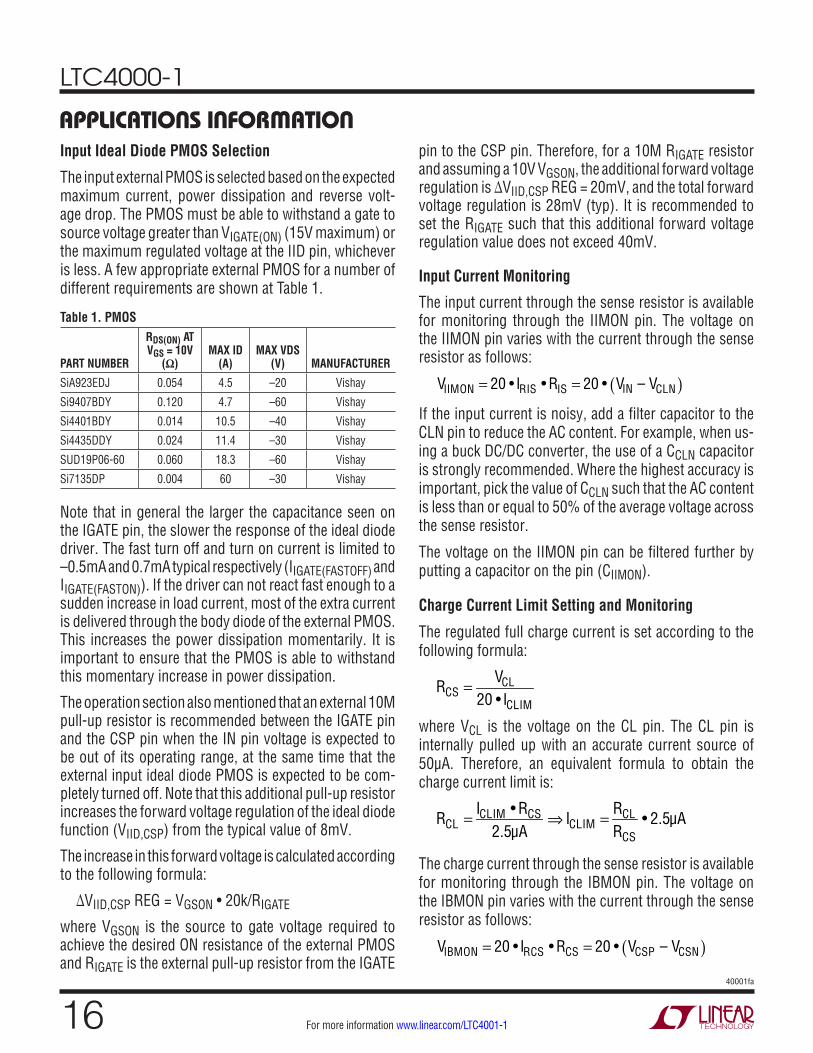
LTC4000-1 1 40001fa For more information www.linear.com/LTC4001-1 Solar Panel Input Regulation, Achieves Max Power Point to Greater than 98% TYPICAL APPLICATION FEATURES DESCRIPTION High Voltage High Current Controller for Battery Charging with Maximum Power Point Control The LTC ® 4000-1 is a high voltage, high performance controller that converts many externally compensated DC/DC power supplies into full-featured battery chargers with maximum power point control. In contrast to the LTC4000, the LTC4000-1 has an input voltage regulation loop instead of the input current regulation loop. Features of the LTC4000-1’s battery charger include: accurate (±0.25%) programmable float voltage, select- able timer or current termination, temperature qualified charging using an NTC thermistor, automatic recharge, C/10 trickle charge for deeply discharged cells, bad battery detection and status indicator outputs. The battery charger also includes precision current sensing that allows lower sense voltages for high current applications. The LTC4000-1 supports intelligent PowerPath control. An external PFET provides low loss reverse current protec- tion. Another external PFET provides low loss charging or discharging of the battery. This second PFET also facilitates an instant-on feature that provides immediate downstream system power even when connected to a heavily discharged or shorted battery. The LTC4000-1 is available in a low profile 28-lead 4mm × 5mm QFN and SSOP packages. 10.8V at 10A Charger for Three LiFePO 4 Cells with a Solar Panel Input APPLICATIONS n Maximum Power Control: Solar Panel Input Compatible n Complete High Performance Battery Charger When Paired with a DC/DC Converter n Wide Input and Output Voltage Range: 3V to 60V n Input Ideal Diode for Low Loss Reverse Blocking and Load Sharing n Output Ideal Diode for Low Loss PowerPath™ and Load Sharing with the Battery n Programmable Charge Current: ±1% Accuracy n ±0.25% Accurate Programmable Float Voltage n Programmable C/X or Timer Based Charge Termination n NTC Input for Temperature Qualified Charging n 28-Lead 4mm × 5mm QFN or SSOP Packages n Solar Powered Battery Charger Systems n Battery Charger with High Impedance Input Source, e.g., Fuel Cell or Wind Turbine n Battery Equipped Industrial or Portable Military Equipments L, LT, LTC, LTM, Linear Technology and the Linear logo are registered trademarks and PowerPath is a trademark of Linear Technology Corporation. All other trademarks are the property of their respective owners. 1.13M 14.7k 127k 10k 10k 3-CELL LiFePO 4 BATTERY PACK V BAT 10.8V FLOAT 10A MAX CHARGE CURRENT 1.15M 47nF 5mΩ V OUT 12V, 15A SOLAR PANEL INPUT <60V OPEN CIRCUIT VOLTAGE 17.6V PEAK POWER VOLTAGE Si7135DP 133k CSN CSP BGATE IGATE BAT OFB FBG BFB NTC CX LTC4000-1 ITH CC IID 5mΩ LT3845A 100μF OUT V C IN CLN IN IFB 22.1k TMR IIMON GND BIAS CL 24.9k 1μF 3V 332k 20k 1μF 10nF 40001 TA01a Si7135DP 0.1μF CHARGER OUTPUT CURRENT: I RCS (A) 1 10 INPUT REGULATION VOLTAGE: V INREG (V) 12 16 14 18 20 5 6 7 8 9 40001 TA01b 10 2 3 4 T A = 25°C 98% TO 95% PEAK POWER 100% TO 98% PEAK POWER
Transcript of LTC4000-1 - High Voltage High Current Controller for ... · to Greater than 98% Typical applicaTion...

LTC4000-1
140001fa
For more information www.linear.com/LTC4001-1
Solar Panel Input Regulation, Achieves Max Power Point
to Greater than 98%
Typical applicaTion
FeaTures DescripTion
High Voltage High Current Controller for Battery Charging with
Maximum Power Point Control
The LTC®4000-1 is a high voltage, high performance controller that converts many externally compensated DC/DC power supplies into full-featured battery chargers with maximum power point control. In contrast to the LTC4000, the LTC4000-1 has an input voltage regulation loop instead of the input current regulation loop.
Features of the LTC4000-1’s battery charger include: accurate (±0.25%) programmable float voltage, select-able timer or current termination, temperature qualified charging using an NTC thermistor, automatic recharge, C/10 trickle charge for deeply discharged cells, bad battery detection and status indicator outputs. The battery charger also includes precision current sensing that allows lower sense voltages for high current applications.
The LTC4000-1 supports intelligent PowerPath control. An external PFET provides low loss reverse current protec-tion. Another external PFET provides low loss charging or discharging of the battery. This second PFET also facilitates an instant-on feature that provides immediate downstream system power even when connected to a heavily discharged or shorted battery.
The LTC4000-1 is available in a low profile 28-lead 4mm × 5mm QFN and SSOP packages.
10.8V at 10A Charger for Three LiFePO4 Cells with a Solar Panel Input
applicaTions
n Maximum Power Control: Solar Panel Input Compatible
n Complete High Performance Battery Charger When Paired with a DC/DC Converter
n Wide Input and Output Voltage Range: 3V to 60Vn Input Ideal Diode for Low Loss Reverse Blocking
and Load Sharingn Output Ideal Diode for Low Loss PowerPath™ and
Load Sharing with the Batteryn Programmable Charge Current: ±1% Accuracyn ±0.25% Accurate Programmable Float Voltagen Programmable C/X or Timer Based Charge
Terminationn NTC Input for Temperature Qualified Chargingn 28-Lead 4mm × 5mm QFN or SSOP Packages
n Solar Powered Battery Charger Systemsn Battery Charger with High Impedance Input Source,
e.g., Fuel Cell or Wind Turbinen Battery Equipped Industrial or Portable Military
EquipmentsL, LT, LTC, LTM, Linear Technology and the Linear logo are registered trademarks and PowerPath is a trademark of Linear Technology Corporation. All other trademarks are the property of their respective owners.
1.13M
14.7k
127k
10k10k 3-CELL LiFePO4
BATTERY PACK
VBAT10.8V FLOAT10A MAX CHARGECURRENT
1.15M47nF
5mΩ
VOUT12V, 15ASOLAR PANEL INPUT
<60V OPEN CIRCUIT VOLTAGE
17.6V PEAK POWER VOLTAGE
Si7135DP
133k
CSNCSP
BGATE
IGATE
BAT
OFB
FBG
BFB
NTC
CX
LTC4000-1
ITH CC IID
5mΩ
LT3845A
100µF
OUTVC
IN
CLNIN
IFB
22.1k
TMRIIMON GND BIASCL
24.9k
1µF
3V
332k
20k
1µF10nF
40001 TA01a
Si7135DP
0.1µF
CHARGER OUTPUT CURRENT: IRCS (A)1
10
INPU
T RE
GULA
TION
VOL
TAGE
: VIN
REG
(V)
12
16
14
18
20
5 6 7 8 9
40001 TA01b
102 3 4
TA = 25°C
98% TO 95% PEAK POWER
100% TO 98% PEAK POWER

LTC4000-1
240001fa
For more information www.linear.com/LTC4001-1
absoluTe MaxiMuM raTings
IN, CLN, IID, CSP, CSN, BAT ....................... –0.3V to 62VIN-CLN, CSP-CSN ............................................–1V to 1VOFB, BFB, FBG ........................................... –0.3V to 62VFBG ............................................................–1mA to 2mA IGATE ...........Max (VIID, VCSP) – 10V to Max (VIID, VCSP)BGATE .......Max (VBAT, VCSN) – 10V to Max (VBAT, VCSN)ENC, CX, NTC, VM ...................................–0.3V to VBIASIFB, CL, TMR, IIMON, CC .........................–0.3V to VBIASBIAS .............................................–0.3V to Min (6V, VIN)
IBMON ..................................–0.3V to Min (VBIAS, VCSP)ITH ............................................................... –0.3V to 6VCHRG, FLT, RST .......................................... –0.3V to 62VCHRG, FLT, RST ..........................................–1mA to 2mAOperating Junction Temperature Range (Note 2) ................................................................. 125°CLead Temperature (Soldering, 10 sec) SSOP Package .................................................. 300°CStorage Temperature Range .................. –65°C to 150°C
(Note 1)
9 10
TOP VIEW
UFD PACKAGE28-LEAD (4mm × 5mm) PLASTIC QFN
11 12 13
28
29GND
27 26 25 24
14
23
6
5
4
3
2
1VM
RST
IIMON
IFB
ENC
IBMON
CX
CL
IGATE
OFB
CSP
CSN
BGATE
BAT
BFB
FBG
GND
IN CLN
CC ITH
IID
TMR
GND
FLT
CHRG
BIAS NT
C
7
17
18
19
20
21
22
16
8 15
TJMAX = 125°C, θJA = 43°C/W, θJC = 4°C/W
EXPOSED PAD (PIN 29) IS GND, MUST BE SOLDERED TO PCB
1
2
3
4
5
6
7
8
9
10
11
12
13
14
TOP VIEW
GN PACKAGE28-LEAD PLASTIC SSOP
28
27
26
25
24
23
22
21
20
19
18
17
16
15
ENC
IBMON
CX
CL
TMR
GND
FLT
CHRG
BIAS
NTC
FBG
BFB
BAT
BGATE
IFB
IIMON
RST
VM
GND
IN
CLN
CC
ITH
IID
IGATE
OFB
CSP
CSN
TJMAX = 125°C, θJA = 80°C/W, θJC = 25°C/W
pin conFiguraTion
orDer inForMaTionLEAD FREE FINISH TAPE AND REEL PART MARKING* PACKAGE DESCRIPTION TEMPERATURE RANGE
LTC4000EUFD-1#PBF LTC4000EUFD-1#TRPBF 40001 28-Lead (4mm × 5mm) Plastic QFN –40°C to 125°C
LTC4000IUFD-1#PBF LTC4000IUFD-1#TRPBF 40001 28-Lead (4mm × 5mm) Plastic QFN –40°C to 125°C
LTC4000EGN-1#PBF LTC4000EGN-1#TRPBF LTC4000GN-1 28-Lead Plastic SSOP –40°C to 125°C
LTC4000IGN-1#PBF LTC4000IGN-1#TRPBF LTC4000GN-1 28-Lead Plastic SSOP –40°C to 125°C
Consult LTC Marketing for parts specified with wider operating temperature ranges. *The temperature grade is identified by a label on the shipping container. Consult LTC Marketing for information on non-standard lead based finish parts.For more information on lead free part marking, go to: http://www.linear.com/leadfree/ For more information on tape and reel specifications, go to: http://www.linear.com/tapeandreel/
LTC4000-1
340001fa
For more information www.linear.com/LTC4001-1
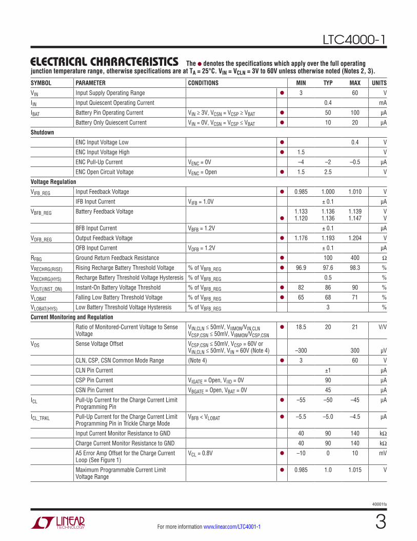
elecTrical characTerisTics The l denotes the specifications which apply over the full operating junction temperature range, otherwise specifications are at TA = 25°C. VIN = VCLN = 3V to 60V unless otherwise noted (Notes 2, 3).
SYMBOL PARAMETER CONDITIONS MIN TYP MAX UNITS
VIN Input Supply Operating Range l 3 60 V
IIN Input Quiescent Operating Current 0.4 mA
IBAT Battery Pin Operating Current VIN ≥ 3V, VCSN = VCSP ≥ VBAT l 50 100 µA
Battery Only Quiescent Current VIN = 0V, VCSN = VCSP ≤ VBAT l 10 20 μA
Shutdown
ENC Input Voltage Low l 0.4 V
ENC Input Voltage High l 1.5 V
ENC Pull-Up Current VENC = 0V –4 –2 –0.5 µA
ENC Open Circuit Voltage VENC = Open l 1.5 2.5 V
Voltage Regulation
VIFB_REG Input Feedback Voltage l 0.985 1.000 1.010 V
IFB Input Current VIFB = 1.0V ± 0.1 µA
VBFB_REG Battery Feedback Voltage
l
1.133 1.120
1.136 1.136
1.139 1.147
V V
BFB Input Current VBFB = 1.2V ± 0.1 µA
VOFB_REG Output Feedback Voltage l 1.176 1.193 1.204 V
OFB Input Current VOFB = 1.2V ± 0.1 µA
RFBG Ground Return Feedback Resistance l 100 400 Ω
VRECHRG(RISE) Rising Recharge Battery Threshold Voltage % of VBFB_REG l 96.9 97.6 98.3 %
VRECHRG(HYS) Recharge Battery Threshold Voltage Hysteresis % of VBFB_REG 0.5 %
VOUT(INST_ON) Instant-On Battery Voltage Threshold % of VBFB_REG l 82 86 90 %
VLOBAT Falling Low Battery Threshold Voltage % of VBFB_REG l 65 68 71 %
VLOBAT(HYS) Low Battery Threshold Voltage Hysteresis % of VBFB_REG 3 %
Current Monitoring and Regulation
Ratio of Monitored-Current Voltage to Sense Voltage
VIN,CLN ≤ 50mV, VIIMON/VIN,CLN VCSP,CSN ≤ 50mV, VIBMON/VCSP,CSN
l 18.5 20 21 V/V
VOS Sense Voltage Offset VCSP,CSN ≤ 50mV, VCSP = 60V or VIN,CLN ≤ 50mV, VIN = 60V (Note 4)
–300
300
µV
CLN, CSP, CSN Common Mode Range (Note 4) l 3 60 V
CLN Pin Current ±1 µA
CSP Pin Current VIGATE = Open, VIID = 0V 90 μA
CSN Pin Current VBGATE = Open, VBAT = 0V 45 μA
ICL Pull-Up Current for the Charge Current Limit Programming Pin
l –55 –50 –45 μA
ICL_TRKL Pull-Up Current for the Charge Current Limit Programming Pin in Trickle Charge Mode
VBFB < VLOBAT l –5.5 –5.0 –4.5 μA
Input Current Monitor Resistance to GND 40 90 140 kΩ
Charge Current Monitor Resistance to GND 40 90 140 kΩ
A5 Error Amp Offset for the Charge Current Loop (See Figure 1)
VCL = 0.8V l –10 0 10 mV
Maximum Programmable Current Limit Voltage Range
l 0.985 1.0 1.015 V
LTC4000-1
440001fa
For more information www.linear.com/LTC4001-1
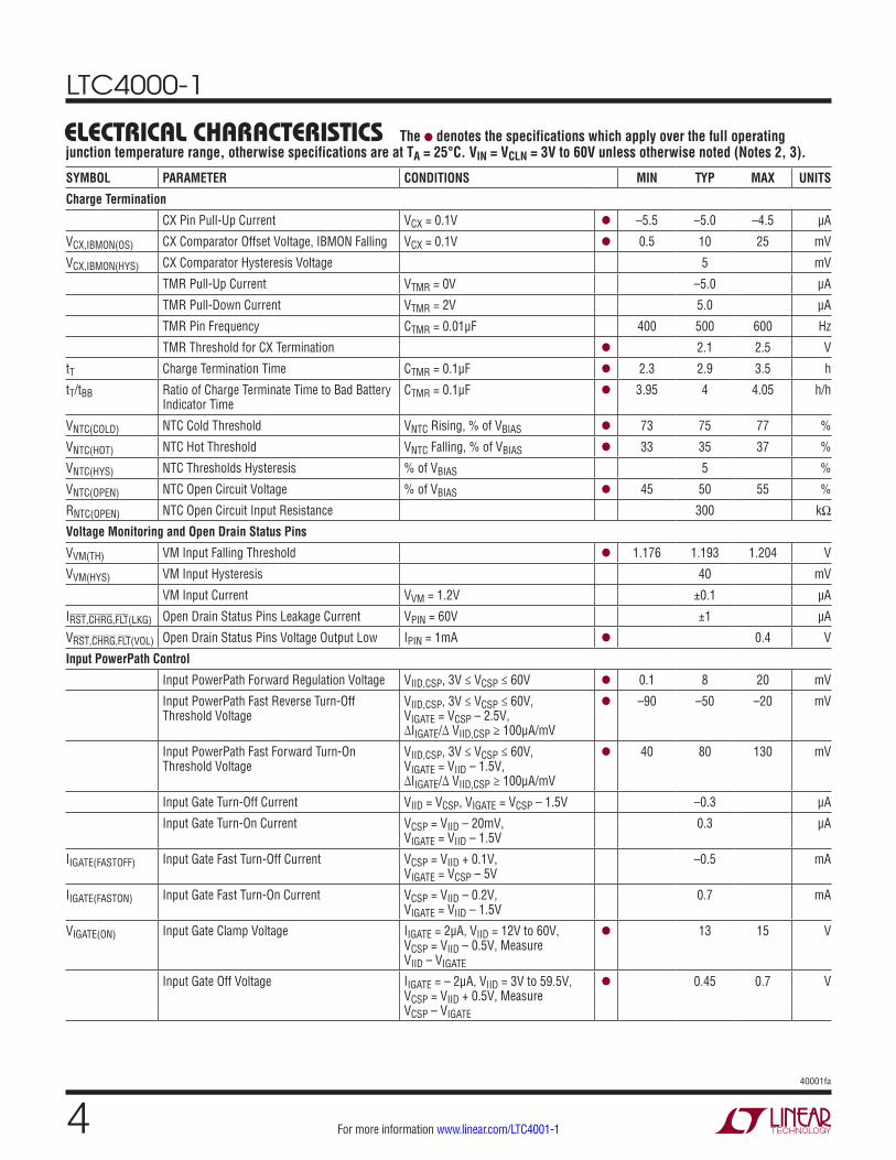
elecTrical characTerisTics The l denotes the specifications which apply over the full operating junction temperature range, otherwise specifications are at TA = 25°C. VIN = VCLN = 3V to 60V unless otherwise noted (Notes 2, 3).
SYMBOL PARAMETER CONDITIONS MIN TYP MAX UNITS
Charge Termination
CX Pin Pull-Up Current VCX = 0.1V l –5.5 –5.0 –4.5 µA
VCX,IBMON(OS) CX Comparator Offset Voltage, IBMON Falling VCX = 0.1V l 0.5 10 25 mV
VCX,IBMON(HYS) CX Comparator Hysteresis Voltage 5 mV
TMR Pull-Up Current VTMR = 0V –5.0 μA
TMR Pull-Down Current VTMR = 2V 5.0 μA
TMR Pin Frequency CTMR = 0.01μF 400 500 600 Hz
TMR Threshold for CX Termination l 2.1 2.5 V
tT Charge Termination Time CTMR = 0.1μF l 2.3 2.9 3.5 h
tT/tBB Ratio of Charge Terminate Time to Bad Battery Indicator Time
CTMR = 0.1μF l 3.95 4 4.05 h/h
VNTC(COLD) NTC Cold Threshold VNTC Rising, % of VBIAS l 73 75 77 %
VNTC(HOT) NTC Hot Threshold VNTC Falling, % of VBIAS l 33 35 37 %
VNTC(HYS) NTC Thresholds Hysteresis % of VBIAS 5 %
VNTC(OPEN) NTC Open Circuit Voltage % of VBIAS l 45 50 55 %
RNTC(OPEN) NTC Open Circuit Input Resistance 300 kΩ
Voltage Monitoring and Open Drain Status Pins
VVM(TH) VM Input Falling Threshold l 1.176 1.193 1.204 V
VVM(HYS) VM Input Hysteresis 40 mV
VM Input Current VVM = 1.2V ±0.1 µA
IRST,CHRG,FLT(LKG) Open Drain Status Pins Leakage Current VPIN = 60V ±1 µA
VRST,CHRG,FLT(VOL) Open Drain Status Pins Voltage Output Low IPIN = 1mA l 0.4 V
Input PowerPath Control
Input PowerPath Forward Regulation Voltage VIID,CSP, 3V ≤ VCSP ≤ 60V l 0.1 8 20 mV
Input PowerPath Fast Reverse Turn-Off Threshold Voltage
VIID,CSP, 3V ≤ VCSP ≤ 60V, VIGATE = VCSP – 2.5V, ∆IIGATE/∆ VIID,CSP ≥ 100μA/mV
l –90 –50 –20 mV
Input PowerPath Fast Forward Turn-On Threshold Voltage
VIID,CSP, 3V ≤ VCSP ≤ 60V, VIGATE = VIID – 1.5V, ∆IIGATE/∆ VIID,CSP ≥ 100μA/mV
l 40 80 130 mV
Input Gate Turn-Off Current VIID = VCSP, VIGATE = VCSP – 1.5V –0.3 μA
Input Gate Turn-On Current VCSP = VIID – 20mV, VIGATE = VIID – 1.5V
0.3 μA
IIGATE(FASTOFF) Input Gate Fast Turn-Off Current VCSP = VIID + 0.1V, VIGATE = VCSP – 5V
–0.5 mA
IIGATE(FASTON) Input Gate Fast Turn-On Current VCSP = VIID – 0.2V, VIGATE = VIID – 1.5V
0.7 mA
VIGATE(ON) Input Gate Clamp Voltage IIGATE = 2µA, VIID = 12V to 60V, VCSP = VIID – 0.5V, Measure VIID – VIGATE
l 13 15 V
Input Gate Off Voltage IIGATE = – 2μA, VIID = 3V to 59.5V, VCSP = VIID + 0.5V, Measure VCSP – VIGATE
l 0.45 0.7 V

LTC4000-1
540001fa
For more information www.linear.com/LTC4001-1
Note 1: Stresses beyond those listed under Absolute Maximum Ratings may cause permanent damage to the device. Exposure to any Absolute Maximum Rating condition for extended periods may affect device reliability and lifetime.Note 2: The LTC4000-1 is tested under conditions such that TJ ≈ TA. The LTC4000E-1 is guaranteed to meet specifications from 0°C to 85°C junction temperature. Specifications over the –40°C to 125°C operating junction temperature range are assured by design, characterization and correlation with statistical process controls. The LTC4000I-1 is guaranteed over the full –40°C to 125°C operating junction temperature range. Note that the maximum ambient temperature consistent with
elecTrical characTerisTics The l denotes the specifications which apply over the full operating junction temperature range, otherwise specifications are at TA = 25°C. VIN = VCLN = 3V to 60V unless otherwise noted (Notes 2, 3).
SYMBOL PARAMETER CONDITIONS MIN TYP MAX UNITS
Battery PowerPath Control
Battery Discharge PowerPath Forward Regulation Voltage
VBAT,CSN, 2.8V ≤ VBAT ≤ 60V l 0.1 8 20 mV
Battery PowerPath Fast Reverse Turn-Off Threshold Voltage
VBAT,CSN, 2.8V ≤ VBAT ≤ 60V, Not Charging, VBGATE = VCSN – 2.5V, ∆IBGATE/∆VBAT,CSN ≥ 100μA/mV
l –90 –50 –20 mV
Battery PowerPath Fast Forward Turn-On Threshold Voltage
VBAT,CSN, 2.8V ≤ VCSN ≤ 60V, VBGATE = VBAT – 1.5V, ∆IBGATE/∆ VBAT,CSN ≥ 100μA/mV
l 40 80 130 mV
Battery Gate Turn-Off Current VBGATE = VCSN – 1.5V, VCSN ≥ VBAT, VOFB < VOUT(INST_ON) and Charging in Progress, or VCSN = VBAT and Not Charging
–0.3 μA
Battery Gate Turn-On Current VBGATE = VBAT – 1.5V, VCSN ≥ VBAT, VOFB > VOUT(INST_ON) and Charging in Progress, or VCSN = VBAT – 20mV
0.3 μA
IBGATE(FASTOFF) Battery Gate Fast Turn-Off Current VCSN = VBAT + 0.1V and Not Charging, VBGATE = VCSN – 5V
–0.5 mA
IBGATE(FASTON) Battery Gate Fast Turn-On Current VCSN = VBAT – 0.2V, VBGATE = VBAT – 1.5V
0.7 mA
VBGATE(ON) Battery Gate Clamp Voltage IBGATE = 2μA, VBAT = 12V to 60V, VCSN = VBAT – 0.5V, Measure VBAT – VBGATE
l 13 15 V
Battery Gate Off Voltage IBGATE = – 2μA, VBAT = 2.8V to 59.5V, VCSN = VBAT + 0.5V and not Charging, Measure VCSN – VBGATE
l 0.45 0.7 V
BIAS Regulator Output and Control Pins
VBIAS BIAS Output Voltage No Load l 2.4 2.9 3.5 V
∆VBIAS BIAS Output Voltage Load Regulation IBIAS = – 0.5mA –0.5 –10 %
BIAS Output Short-Circuit Current VBIAS = 0V –20 mA
Transconductance of Error Amp CC = 1V 0.5 mA/V
Open Loop DC Voltage Gain of Error Amp CC = Open 80 dB
IITH(PULL_UP) Pull-Up Current on the ITH Pin VITH = 0V, CC = 0V –6 –5 –4 μA
IITH(PULL_DOWN) Pull-Down Current on the ITH Pin VITH = 0.4V, CC = Open l 0.5 1 mA
Open Loop DC Voltage Gain of ITH Driver ITH = Open 60 dB
these specifications is determined by specific operating conditions in conjunction with board layout, the rated package thermal impedance and other environmental factors. The junction temperature (TJ, in °C) is calculated from the ambient temperature (TA, in °C) and power dissipation (PD, in Watts) according to the following formula: TJ = TA + (PD • θJA), where θJA (in °C/W) is the package thermal impedance.Note 3: All currents into pins are positive; all voltages are referenced to GND unless otherwise noted.Note 4: These parameters are guaranteed by design and are not 100% tested.
LTC4000-1
640001fa
For more information www.linear.com/LTC4001-1
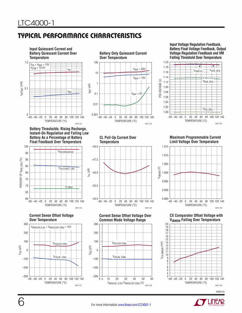
Typical perForMance characTerisTics
Battery Thresholds: Rising Recharge, Instant-On Regulation and Falling Low Battery As a Percentage of Battery Float Feedback Over Temperature
CL Pull-Up Current Over Temperature
Maximum Programmable Current Limit Voltage Over Temperature
Input Quiescent Current and Battery Quiescent Current Over Temperature
Battery Only Quiescent Current Over Temperature
Input Voltage Regulation Feedback, Battery Float Voltage Feedback, Output Voltage Regulation Feedback and VM Falling Threshold Over Temperature
TEMPERATURE (°C)–60
I BAT
(µA)
100
0.1
0.01
10
1
0.00110020
40001 G02
14040 60 80–20 0–40 120
VBAT = 3V
VBAT = 60V
VBAT = 15V
TEMPERATURE (°C)–60
PIN
VOLT
AGE
(V)
1.20
1.12
1.18
1.16
1.14
1.00
1.02
1.08
1.06
1.04
1.00
10020
40001 G03
14040 60 80–20 0–40 120
VBFB_REG
VIFB_REG
VVM(TH) VOFB_REG
TEMPERATURE (°C)–60
V IBM
ON (V
)
1.015
1.010
0.995
1.000
0.990
1.005
0.98510020
40001 G06
14040 60 80–20 0–40 120TEMPERATURE (°C)
–60
PERC
ENT
OF V
BFB_
REG
(%)
100
85
95
90
65
75
80
70
6010020
40001 G04
14040 60 80–20 0–40 120
VLOBAT
VRECHRG(RISE)
VOUT(INST_ON)
TEMPERATURE (°C)–60
I CL
(µA)
–45.0
–47.5
–52.5
–50.0
–55.010020
40001 G05
14040 60 80–20 0–40 120
TEMPERATURE (°C)–60 –20–40
I IN/I B
AT (m
A)
1.0
0.1
080 10020 40
40001 G01
140600 120
IIN
IBAT
VIN = VBAT = 15VVCSN = 15.5V
CX Comparator Offset Voltage with VIBMON Falling Over Temperature
TEMPERATURE (°C)–60
V OS
(µV)
300
200
–100
0
–200
100
–30010020
40001 G07
14040 60 80–20 0–40 120
VOS(CSP, CSN)
VOS(IN, CSN)
VMAX(IN,CLN) = VMAX(CSP, CSN) = 15V
Current Sense Offset Voltage Over Common Mode Voltage Range
Current Sense Offset Voltage Over Temperature
VMAX(IN, CLN)/VMAX(CSP, CSN) (V)0
V OS
(µV)
300
200
–100
0
–200
100
–300
40001 G08
6030 40 5020103
VOS(CSP, CSN)
VOS(IN, CSN)
TEMPERATURE (°C)–60
V CX,
IBM
ON (m
V)
2019
567
4
910
8
1817161514131211
310020
40001 G09
14040 60 80–20 0–40 120
LTC4000-1
740001fa
For more information www.linear.com/LTC4001-1
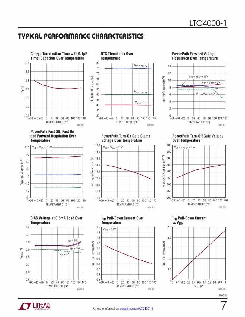
Typical perForMance characTerisTics
PowerPath Forward Voltage Regulation Over Temperature
Charge Termination Time with 0.1µF Timer Capacitor Over Temperature
NTC Thresholds Over Temperature
TEMPERATURE (°C)–60
T T (h
)
3.5
3.3
3.1
2.9
2.7
2.5
2.310020
40001 G10
14040 60 80–20 0–40 120TEMPERATURE (°C)
–60
PERC
ENT
OF V
BIAS
(%)
80
65
75
70
45
55
60
50
40
35
3010020
40001 G11
14040 60 80–20 0–40 120
VNTC(OPEN)
VNTC(HOT)
VNTC(COLD)
TEMPERATURE (°C)–60
V IID
,CSP
/VBA
T,CSN
(mV)
14
6
10
12
8
4
2
010020
40001 G12
14040 60 80–20 0–40 120
VIID = VBAT = 60V
VIID = VBAT = 3V
VIID = VBAT = 15V
PowerPath Turn-Off Gate Voltage Over Temperature
BIAS Voltage at 0.5mA Load Over Temperature
ITH Pull-Down Current Over Temperature
PowerPath Fast Off, Fast On and Forward Regulation Over Temperature
PowerPath Turn-On Gate Clamp Voltage Over Temperature
TEMPERATURE (°C)–60
V IID
,CSP
/VBA
T,CSN
(mV)
120
0
60
90
30
–30
–60
–9010020
40001 G13
14040 60 80–20 0–40 120
VIID = VBAT = 15V
TEMPERATURE (°C)–60
V IGA
TE(O
N)/V
BGAT
E(ON
) (V)
15.0
12.5
13.5
14.5
14.0
13.0
12.0
11.5
11.010020
40001 G14
14040 60 80–20 0–40 120
VIID = VBAT = 15V
TEMPERATURE (°C)–60
V CSP
,IGAT
E/V C
SN,B
GATE
(mV)
600
350
450
550
500
400
300
250
20010020
40001 G15
14040 60 80–20 0–40 120
VCSP = VCSN = 15V
TEMPERATURE (°C)–60
V BIA
S (V
)
3.2
2.8
3.0
3.1
2.9
2.7
2.6
2.510020
40001 G16
14040 60 80–20 0–40 120
VIN = 60V
VIN = 15V
VIN = 3V
TEMPERATURE (°C)–60
I ITH(
PULL
-DOW
N) (m
A)
1.5
0.8
1.0
1.1
1.2
1.3
1.4
0.9
0.7
0.6
0.510020
40001 G17
14040 60 80–20 0–40 120
VITH = 0.4V
ITH Pull-Down Current vs VITH
VITH (V)0
I ITH(
PULL
-DOW
N) (m
A)
2.5
1.5
2.0
1.0
0.5
00.80.4
40001 G18
10.5 0.6 0.70.2 0.30.1 0.9

LTC4000-1
840001fa
For more information www.linear.com/LTC4001-1
pin FuncTionsVM (Pin 1/Pin 25): Voltage Monitor Input. High impedance input to an accurate comparator with a 1.193V threshold (typical). This pin controls the state of the RST output pin. Connect a resistor divider (RVM1, RVM2) between the monitored voltage and GND, with the center tap point con-nected to this pin. The falling threshold of the monitored voltage is calculated as follows:
VVM _RST = RVM1 +RVM2
RVM2• 1.193V
where RVM2 is the bottom resistor between the VM pin and GND. Tie to the BIAS pin if voltage monitoring func-tion is not used.
RST (Pin 2/Pin 26): High Voltage Open Drain Reset Output. When the voltage at the VM pin is below 1.193V, this status pin is pulled low. When driven low, this pin can disable a DC/DC converter when connected to the converter’s enable pin. This pin can also drive an LED to provide a visual status indicator of a monitored voltage. Short this pin to GND when not used.
IIMON (Pin 3/Pin 27): Input Current Monitor. The voltage on this pin is 20 times (typical) the sense voltage (VIN,CLN) across the input current sense resistor(RIS), therefore providing a voltage proportional to the input current. Connect an appropriate capacitor to this pin to obtain a voltage representation of the time-average input current. Leave this pin open when input current monitoring func-tion is not needed.
IFB (Pin 4/Pin 28): Input Voltage Feedback Pin. This pin is a high impedance input pin used to sense the input voltage level. In regulation, the input voltage loop sets the voltage on this feedback pin to 1.000V. When the input feedback voltage drops below 1.000V, the ITH pin is pulled down to reduce the load on the input source. Connect this pin to the center node of a resistor divider between the IN pin and GND to set the input voltage regulation level. This regulation level can then be obtained as follows:
VIN _REG =
ROFB1ROFB2
+ 1
• 1.000V
If the input voltage regulation feature is not used, connect the IFB pin to the BIAS pin.
ENC (Pin 5/Pin 1): Enable Charging Pin. High impedance digital input pin. Pull this pin above 1.5V to enable charg-ing and below 0.5V to disable charging. Leaving this pin open causes the internal 2µA pull-up current to pull the pin to 2.5V (typical).
IBMON (Pin 6/Pin 2): Battery Charge Current Monitor. The voltage on this pin is 20 times (typical) the sense voltage (VCSP,CSN) across the battery current sense resistor (RCS), therefore providing a voltage proportional to the battery charge current. Connect an appropriate capacitor to this pin to obtain a voltage representation of the time-average battery charge current. Short this pin to GND to disable charge current limit feature.
CX (Pin 7/Pin 3): Charge Current Termination Pro-gramming. Connect the charge current termination pro-gramming resistor (RCX) to this pin. This pin is a high impedance input to a comparator and sources 5μA of current. When the voltage on this pin is greater than the charge current monitor voltage (VIBMON), the CHRG pin turns high impedance indicating that the CX threshold is reached. When this occurs, the charge current is imme-diately terminated if the TMR pin is shorted to the BIAS pin, otherwise charging continues until the charge termi-nation timer expires. The charge current termination value is determined using the following formula:
IC/X =
0.25µA • RCX( ) − 0.5mV
RCS
Where RCS is the sense resistor connected to the CSP and the CSN pins. Note that if RCX = RCL ≤ 19.1kΩ, where RCL is the charge current programming resistor, then the charge current termination value is one tenth the full charge current, more familiarly known as C/10. Short this pin to GND to disable CX termination.
CL (Pin 8/Pin 4): Charge Current Limit Programming. Con-nect the charge current programming resistor (RCL) to this pin. This pin sources 50µA of current. The regulation loop compares the voltage on this pin with the charge current monitor voltage (VIBMON), and drives the ITH pin accord-ingly to ensure that the programmed charge current limit
(QFN/SSOP)

LTC4000-1
940001fa
For more information www.linear.com/LTC4001-1
pin FuncTions (QFN/SSOP)
is not exceeded. The charge current limit is determined using the following formula:
ICLIM = 2.5µA •
RCL
RCS
Where RCS is the sense resistor connected to the CSP and the CSN pins. Leave the pin open for the maximum charge current limit of 50mV/RCS.
TMR (Pin 9/Pin 5): Charge Timer. Attach 1nF of external capacitance (CTMR) to GND for each 104 seconds of charge termination time and 26 seconds of bad battery indicator time. Short to GND to prevent bad battery indicator time and charge termination time from expiring – allowing a continuous trickle charge and top off float voltage regula-tion charge. Short to BIAS to disable bad battery detect and enable C/X charging termination.
GND (Pins 10, 28, 29/Pins 6, 24): Device Ground Pins. Connect the ground pins to a suitable PCB copper ground plane for proper electrical operation. The QFN package exposed pad must be soldered to PCB ground for rated thermal performance.
FLT, CHRG (Pin 11, Pin 12/Pin 7, Pin 8): Charge Status Indicator Pins. These pins are high voltage open drain pull down pins. The FLT pin pulls down when there is an under or over temperature condition during charging or when the voltage on the BFB pin stays below the low battery threshold during charging for a period longer than the bad battery indicator time. The CHRG pin pulls down during a charging cycle. Please refer to the application informa-tion section for details on specific modes indicated by the combination of the states of these two pins. Pull up each of these pins with an LED in series with a resistor to a voltage source to provide a visual status indicator. Short these pins to GND when not used.
BIAS (Pin 13/Pin 9): 2.9V Regulator Output. Connect a capacitor of at least 470nF to bypass this 2.9V regulated voltage output. Use this pin to bias the resistor divider to set up the voltage at the NTC pin.
NTC (Pin 14/Pin 10): Thermistor Input. Connect a ther-mistor from NTC to GND, and a corresponding resistor from BIAS to NTC. The voltage level on this pin determines
if the battery temperature is safe for charging. The charge current and charge timer are suspended if the thermistor indicates a temperature that is unsafe for charging. Once the temperature returns to the safe region, charging resumes. Leave the pin open or connected to a capacitor to disable the temperature qualified charging function.
FBG (Pin 15/Pin 11): Feedback Ground Pin. This is the ground return pin for the resistor dividers connected to the BFB and OFB pins. As soon as the voltage at IN is valid (>3V typical), this pin has a 100Ω resistance to GND. When the voltage at IN is not valid, this pin is disconnected from GND to ensure that the resistor dividers connected to the BFB and OFB pins do not continue to drain the battery when the battery is the only available power source.
BFB (Pin 16/Pin 12): Battery Feedback Voltage Pin. This pin is a high impedance input pin used to sense the battery voltage level. In regulation, the battery float voltage loop sets the voltage on this pin to 1.136V (typical). Connect this pin to the center node of a resistor divider between the BAT pin and the FBG pin to set the battery float voltage. The battery float voltage can then be obtained as follows:
VFLOAT = RBFB2 +RBFB1
RBFB2• 1.136V
BAT (Pin 17/Pin 13): Battery Pack Connection. Connect the battery to this pin. This pin is the anode of the battery ideal diode driver (the cathode is the CSN pin).
BGATE (Pin 18/Pin 14): External Battery PMOS Gate Drive Output. When not charging, the BGATE pin drives the external PMOS to behave as an ideal diode from the BAT pin (anode) to the CSN pin (cathode). This allows efficient delivery of any required additional power from the battery to the downstream system connected to the CSN pin.
When charging a heavily discharged battery, the BGATE pin is regulated to set the output feedback voltage (OFB pin) to 86% of the battery float voltage (0.974V typical). This allows the instant-on feature, providing an immediate valid voltage level at the output when the LTC4000-1 is charging a heavily discharged battery. Once the voltage on the OFB pin is above the 0.974V typical value, then the BGATE pin is driven low to ensure an efficient charging path from the CSN pin to the BAT pin.

LTC4000-1
1040001fa
For more information www.linear.com/LTC4001-1
CSN (Pin 19/Pin 15): Charge Current Sense Negative Input and Battery Ideal Diode Cathode. Connect a sense resistor between this pin and the CSP pin. The LTC4000-1 senses the voltage across this sense resistor and regulates it to a voltage equal to 1/20th (typical) of the voltage set at the CL pin. The maximum regulated sense voltage is 50mV. The CSN pin is also the cathode input of the battery ideal diode driver (the anode input is the BAT pin). Tie this pin to the CSP pin if no charge current limit is desired. Refer to the Applications Information section for complete details.
CSP (Pin 20/Pin 16): Charge Current Sense Positive Input and Input Ideal Diode Cathode. Connect a sense resis-tor between this pin and the CSN pin for charge current sensing and regulation. This input should be tied to CSN to disable the charge current regulation function. This pin is also the cathode of the input ideal diode driver (the anode is the IID pin).
OFB (Pin 21/Pin 17): Output Feedback Voltage Pin. This pin is a high impedance input pin used to sense the output voltage level. In regulation, the output voltage loop sets the voltage on this feedback pin to 1.193V. Connect this pin to the center node of a resistor divider between the CSP pin and the FBG pin to set the output voltage when battery charging is terminated and all the output load current is provided from the input. The output voltage can then be obtained as follows:
VOUT = ROFB2 +ROFB1
ROFB2• 1.193V
When charging a heavily discharged battery (such that VOFB < VOUT(INST_ON)), the battery PowerPath PMOS connected to BGATE is regulated to set the voltage on this feedback pin to 0.974V (approximately 86% of the battery float voltage). The instant-on output voltage is then as follows:
VOUT(INST _ ON) = ROFB2 +ROFB1
ROFB2• 0.974V
IGATE (Pin 22/Pin 18): Input PMOS Gate Drive Output. The IGATE pin drives the external PMOS to behave as an ideal diode from the IID pin (anode) to the CSP pin (cathode) when the voltage at the IN pin is within its operating range
(3V to 60V). To ensure that the input PMOS is turned off when the IN pin voltage is not within its operating range, connect a 10M resistor from this pin to the CSP pin.
IID (Pin 23/Pin 19): Input Ideal Diode Anode. This pin is the anode of the input ideal diode driver (the cathode is the CSP pin).
ITH (Pin 24/Pin 20): High Impedance Control Voltage Pin. When any of the regulation loops (input voltage, charge current, battery float voltage or the output voltage) indicate that its limit is reached, the ITH pin will sink current (up to 1mA) to regulate that particular loop at the limit. In many applications, this ITH pin is connected to the control/compensation node of a DC/DC converter. Without any external pull-up, the operating voltage range on this pin is GND to 2.5V. With an external pull-up, the voltage on this pin can be pulled up to 6V. Note that the impedance connected to this pin affects the overall loop gain. For details, refer to the Applications Information section.
CC (Pin 25/Pin 21): Converter Compensation Pin. Connect an R-C network from this pin to the ITH pin to provide a suitable loop compensation for the converter used. Refer to the Applications Information section for discussion and procedure on choosing an appropriate R-C network for a particular DC/DC converter.
CLN (Pin 26/Pin 22): Input Current Sense Negative Input. Connect a sense resistor between this pin and the IN pin. The LTC4000-1 senses the voltage across this sense resistor and sets the voltage on the IIMON pin equal to 20 times this voltage. Tie this pin to the IN pin if the input current monitoring feature is not used. Refer to the Applications Information section for complete details.
IN (Pin 27/Pin 23): Input Supply Voltage: 3V to 60V. Supplies power to the internal circuitry and the BIAS pin. Connect the power source to the downstream system and the battery charger to this pin. This pin is also the positive sense pin for the input current monitor. Connect a sense resistor between this pin and the CLN pin. Tie this pin to CLN if the input current monitoring feature is not used. A local 0.1µF bypass capacitor to ground is recommended on this pin.
pin FuncTions (QFN/SSOP)
LTC4000-1
1140001fa
For more information www.linear.com/LTC4001-1
RC
RNTC
BATTERY PACK
RCL
CC
RCS
SYSTEMLOAD
IN
CSN
BGATE
IGATE
CL
A2 LINEARGATE
DRIVERAND
VOLTAGECLAMP
ENABLECHARGING
A1
BATTERY IDEAL DIODEAND INSTANT-ON DRIVER
INPUT IDEALDIODE DRIVER
ITH AND CC DRIVER
OFBOFBA7
A4
CP1
1.193V
1V
BFB
FBG
BAT
CX
ITHRSTCLN CC IID
ROFB2
ROFB1
RBFB2
RBFB1
RISDC/DC CONVERTER
IN
CIID
VM
BIAS
TMR
FLTCHRG
CINCCLN CL
CBAT
CTMR
RVM1
RVM2
CIBMON
40001 BD
ENCGND
IBMON
OUT
CSP
RCX
R3
+–
+
–
1V
–+
–+
BIAS
2µA
BIAS
5µA/50µA
CIIMON
IIMON
IFB
IN
A8gm = 0.33m
A9gm = 0.33m
A11
0.974V
gm
BFBA6
1.136V
A10
1.193V
CP5 +
–
1.109V
CP6
+
– 0.771V
CP2
+
–BIAS
5µA
10mV
A5
60k8mV
CBIAS
OSCILLATOR
LOGIC
CP3+
–
+
–
CP4
TOO HOT
NTC FAULT
TOO COLD
NTC
LDO,BG,REF REF
+–
–
–+–
+–
gm
gm
–+gm
gm
gm
8mV
+–
+–
+–
60k
RIFB2
RIFB1
10M
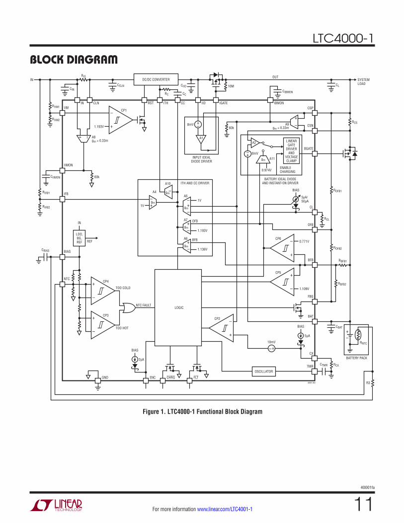
block DiagraM
Figure 1. LTC4000-1 Functional Block Diagram
LTC4000-1
1240001fa
For more information www.linear.com/LTC4001-1
operaTionOverview
The LTC4000-1 is designed to simplify the conversion of any externally compensated DC/DC converter into a high performance battery charger with PowerPath control. It only requires the DC/DC converter to have a control or external-compensation pin (usually named VC or ITH) whose voltage level varies in a positive monotonic way with its output. The output variable can be either output voltage or output current. For the following discussion, refer to the Block Diagram in Figure 1.
The LTC4000-1 includes four different regulation loops: input voltage, charge current, battery float voltage and output voltage (A4-A7). Whichever loop requires the low-est voltage on the ITH pin for its regulation controls the external DC/DC converter.
The input voltage regulation loop ensures that the input voltage level does not drop below the programmed level. The charge current regulation loop ensures that the pro-grammed battery charge current limit (using a resistor at CL) is not exceeded. The float voltage regulation loop ensures that the programmed battery stack voltage (us-ing a resistor divider from BAT to FBG via BFB) is not exceeded. The output voltage regulation loop ensures that the programmed system output voltage (using a resistor divider from CSP to FBG via OFB) is not exceeded. The LTC4000-1 also provides monitoring pins for the input current and charge current at the IIMON and IBMON pins respectively.
The LTC4000-1 features an ideal diode controller at the input from the IID pin to the CSP pin and a PowerPath controller at the output from the BAT pin to the CSN pin. The output PowerPath controller behaves as an ideal diode controller when not charging. When charging, the output PowerPath controller has two modes of operation. If VOFB is greater than VOUT(INST_ON), BGATE is driven low. When VOFB is less than VOUT(INST_ON), a linear regulator implements the instant-on feature. This feature provides regulation of the BGATE pin so that a valid voltage level is immediately available at the output when the LTC4000-1 is charging an over-discharged, dead or short faulted battery.
The state of the ENC pin determines whether charging is enabled. When ENC is grounded, charging is disabled and
the battery float voltage loop is disabled. Charging is enabled when the ENC pin is left floating or pulled high (≥1.5V)
The LTC4000-1 offers several user configurable battery charge termination schemes. The TMR pin can be config-ured for either C/X termination, charge timer termination or no termination. After a particular charge cycle terminates, the LTC4000-1 features an automatic recharge cycle if the battery voltage drops below 97.6% of the programmed float voltage.
Trickle charge mode drops the charge current to one tenth of the normal charge current (programmed using a resistor from the CL pin to GND) when charging into an over discharged or dead battery. When trickle charging, a capacitor on the TMR pin can be used to program a time out period. When this bad battery timer expires and the battery voltage fails to charge above the low battery threshold (VLOBAT), the LTC4000-1 will terminate charging and indicate a bad battery condition through the status pins (FLT and CHRG).
The LTC4000-1 also includes an NTC pin, which provides temperature qualified charging when connected to an NTC thermistor thermally coupled to the battery pack. To enable this feature, connect the thermistor between the NTC and the GND pins, and a corresponding resistor from the BIAS pin to the NTC pin. The LTC4000-1 also provides a charg-ing status indicator through the FLT and the CHRG pins.
Aside from biasing the thermistor-resistor network, the BIAS pin can also be used for a convenient pull up voltage. This pin is the output of a low dropout voltage regulator that is capable of providing up to 0.5mA of current. The regulated voltage on the BIAS pin is available as soon as the IN pin is within its operating range (≥3V).
Input Ideal Diode
The input ideal diode feature provides low loss conduction and reverse blocking from the IID pin to the CSP pin. This reverse blocking prevents reverse current from the output (CSP pin) to the input (IID pin) which causes unneces-sary drain on the battery and in some cases may result in unexpected DC/DC converter behavior.
The ideal diode behavior is achieved by controlling an external PMOS connected to the IID pin (drain) and the
LTC4000-1
1340001fa
For more information www.linear.com/LTC4001-1
operaTionCSP pin (source). The controller (A1) regulates the external PMOS by driving the gate of the PMOS device such that the voltage drop across IID and CSP is 8mV (typical). When the external PMOS ability to deliver a particular current with an 8mV drop across its source and drain is exceeded, the voltage at the gate clamps at VIGATE(ON) and the PMOS behaves like a fixed value resistor (RDS(ON)).
Note that this input ideal diode function is only enabled when the voltage at the IN pin is within its operating range (3V to 60V). To ensure that the external PMOS is turned off when the voltage at the IN pin is not within is operating range, a 10M pull-up resistor between the IGATE and the CSP pin is recommended.
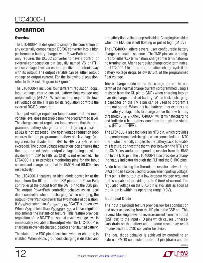
Input Voltage Regulation
One of the loops driving the ITH and CC pins is the input voltage regulation loop (Figure 2). This loop prevents the input voltage from dropping below the programmed level.
When a battery charge cycle begins, the battery charger first determines if the battery is over-discharged. If the battery feedback voltage is below VLOBAT, an automatic trickle charge feature uses the charge current regulation loop to set the battery charge current to 10% of the pro-grammed full-scale value. If the TMR pin is connected to a capacitor or open, the bad battery detection timer is enabled. When this bad battery detection timer expires and the battery voltage is still below VLOBAT, the battery charger automatically terminates and indicates, via the FLT and CHRG pins, that the battery was unresponsive to charge current.
Once the battery voltage is above VLOBAT, the charge current regulation loop begins charging in full power constant-current mode. In this case, the programmed full charge current is set with a resistor on the CL pin.
Depending on available input power and external load conditions, the battery charger may not be able to charge at the full programmed rate. The external load is always prioritized over the battery charge current. The input volt-age programming is always observed, and only additional power is available to charge the battery. When system loads are light, battery charge current is maximized.
Once the float voltage is achieved, the battery float volt-age regulation loop takes over from the charge current regulation loop and initiates constant voltage charging. In constant voltage charging, charge current slowly declines.
Charge termination can be configured with the TMR pin in several ways. If the TMR pin is tied to the BIAS pin, C/X termination is selected. In this case, charging is terminated when constant voltage charging reduces the charge current to the C/X level programmed at the CX pin. Connecting a capacitor to the TMR pin selects the charge timer termination and a charge termination timer is started at the beginning of constant voltage charging. Charging terminates when the termination timer expires. When continuous charging at the float voltage is desired, tie the TMR pin to GND to disable termination.
Upon charge termination, the PMOS connected to BGATE behaves as an ideal diode from BAT to CSN. The diode function prevents charge current but provides current to the system load as needed. If the system load can be completely supplied from the input, the battery PMOS turns
Figure 2. Input Voltage Regulation Loop
IN
CC
1VITH
LTC4000-1IN CLN
RISDC/DC INPUT
CCLN(OPTIONAL)
IFB
CIN
–+
–+
CC
TO DC/DC
40001 FO2
RC
A4RIFB2
RIFB1
When the input source is high impedance, the input volt-age drops as the load current increases. In that case there exists a voltage level at which the available power from the input is maximum. For example, solar panels often specify VMP, corresponding to the panel voltage at which maximum power is achieved. With the LTC4000-1 input voltage regulation, this maximum power voltage level can be programmed at the IFB pin. The input voltage regulation loop regulates ITH to ensure that the input voltage level does not drop below this programmed level.
Battery Charger Overview
In addition to the input voltage regulation loop, the LTC4000-1 regulates charge current, battery voltage and output voltage.
LTC4000-1
1440001fa
For more information www.linear.com/LTC4001-1
operaTionoff. While terminated, if the input voltage loop is not in regulation, the output voltage regulation loop takes over to ensure that the output voltage at CSP remains in control. The output voltage regulation loop regulates the voltage at the CSP pin such that the output feedback voltage at the OFB pin is 1.193V.
If the system load requires more power than is available from the input, the battery ideal diode controller provides supplemental power from the battery. When the battery voltage discharges below 97.1% of the float voltage (VBFB < VRECHRG(FALL)), the automatic recharge feature initiates a new charge cycle.
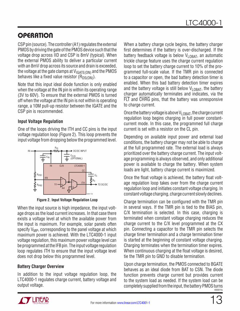
Charge Current Regulation
The first loop involved in a normal charging cycle is the charge current regulation loop (Figure 3). This loop drives the ITH and CC pins. This loop ensures that the charge current sensed through the charge current sense resistor (RCS) does not exceed the programmed full charge current.
tor divider does not consume battery current when the battery is the only available power source. For VIN ≥ 3V, the typical resistance from the FBG pin to GND is 100Ω.
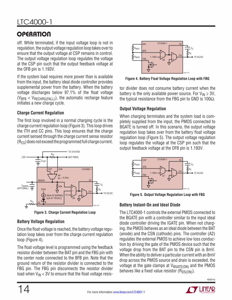
Output Voltage Regulation
When charging terminates and the system load is com-pletely supplied from the input, the PMOS connected to BGATE is turned off. In this scenario, the output voltage regulation loop takes over from the battery float voltage regulation loop (Figure 5). The output voltage regulation loop regulates the voltage at the CSP pin such that the output feedback voltage at the OFB pin is 1.193V.
Figure 3. Charge Current Regulation Loop
Figure 4. Battery Float Voltage Regulation Loop with FBG
Figure 5. Output Voltage Regulation Loop with FBG
CSP
CC
1VA5
ITH
LTC4000-1CSP CSN
RISBAT PMOS
TO SYSTEM
IBMON
CL
CIBMON(OPTIONAL)
CCSP
+ –
–+
+––
CC
TO DC/DC
40001 FO3
RC
60k
50µA AT NORMAL5µA AT TRICKLE
BIAS
A9gm = 0.33m
RCL
CC
1.136VITH
LTC4000-1
BFB
BAT
FBG
–+
CC
TO DC/DC
40001 FO4
RC
RBFB2
RBFB1
A6
+–
CC
1.193VITH
LTC4000-1
OFB
CSP
FBG
–+
CC
TO DC/DC
40001 FO5
RC
ROFB2
ROFB1
A7
+–
Battery Voltage Regulation
Once the float voltage is reached, the battery voltage regu-lation loop takes over from the charge current regulation loop (Figure 4).
The float voltage level is programmed using the feedback resistor divider between the BAT pin and the FBG pin with the center node connected to the BFB pin. Note that the ground return of the resistor divider is connected to the FBG pin. The FBG pin disconnects the resistor divider load when VIN < 3V to ensure that the float voltage resis-
Battery Instant-On and Ideal Diode
The LTC4000-1 controls the external PMOS connected to the BGATE pin with a controller similar to the input ideal diode controller driving the IGATE pin. When not charg-ing, the PMOS behaves as an ideal diode between the BAT (anode) and the CSN (cathode) pins. The controller (A2) regulates the external PMOS to achieve low loss conduc-tion by driving the gate of the PMOS device such that the voltage drop from the BAT pin to the CSN pin is 8mV. When the ability to deliver a particular current with an 8mV drop across the PMOS source and drain is exceeded, the voltage at the gate clamps at VBGATE(ON) and the PMOS behaves like a fixed value resistor (RDS(ON)).

LTC4000-1
1540001fa
For more information www.linear.com/LTC4001-1
operaTionThe ideal diode behavior allows the battery to provide cur-rent to the load when the input supply is in current limit or the DC/DC converter is slow to react to an immediate load increase at the output. In addition to the ideal diode behavior, BGATE also allows current to flow from the CSN pin to the BAT pin during charging.
There are two regions of operation when current is flowing from the CSN pin to the BAT pin. The first is when charging into a battery whose voltage is below the instant-on threshold (VOFB < VOUT(INST_ON)). In this region of operation, the controller regulates the voltage at the CSP pin to be approximately 86% of the final float voltage level (VOUT(INST_ON)). This feature provides a CSP voltage significantly higher than the battery voltage when charging into a heavily discharged battery. This instant-on feature allows the LTC4000-1 to provide sufficient voltage at the output (CSP pin), independent of the battery voltage.
The second region of operation is when the battery feedback voltage is greater than or equal to the instant-on threshold (VOUT(INST_ON)). In this region, the BGATE pin is driven low and clamped at VBGATE(ON) to allow the PMOS to turn completely on, reducing any power dissipation due to the charge current.
Battery Temperature Qualified Charging
The battery temperature is measured by placing a nega-tive temperature coefficient (NTC) thermistor close to the battery pack. The comparators CP3 and CP4 implement the temperature detection as shown in the Block Diagram in Figure 1. The rising threshold of CP4 is set at 75% of VBIAS (cold threshold) and the falling threshold of CP3 is set at 35% of VBIAS (hot threshold). When the voltage at the NTC pin is above 75% of VBIAS or below 35% of VBIAS then the LTC4000-1 pauses any charge cycle in progress. When the voltage at the NTC pin returns to the range of 40% to 70% of VBIAS, charging resumes.
When charging is paused, the external charging PMOS turns off and charge current drops to zero. If the LTC4000-1 is charging in the constant voltage mode and the charge termination timer is enabled, the timer pauses until the thermistor indicates a return to a valid temperature. If the battery charger is in the trickle charge mode and the bad battery detection timer is enabled, the bad battery timer
pauses until the thermistor indicates a return to a valid temperature.
Input UVLO and Voltage Monitoring
The regulated voltage on the BIAS pin is available as soon as VIN ≥ 3V. When VIN ≥ 3V, the FBG pin is pulled low to GND with a typical resistance of 100Ω and the rest of the chip functionality is enabled.
When the IN pin is high impedance and a battery is con-nected to the BAT pin, the BGATE pin is pulled down with a 2μA (typical) current source to hold the battery PMOS gate voltage at VBGATE(ON) below VBAT. This allows the battery to power the output. The total quiescent current consumed by LTC4000-1 from the battery when IN is not valid is typically ≤ 10µA.
When the IN pin is high impedance, the input ideal diode function for the external FET connected to the IGATE pin is disabled. To ensure that this FET is completely turned off when the voltage at the IN pin is not within its operating range, connect a 10M pull-up resistor between the IGATE pin and the CSP pin.
Besides the internal input UVLO, the LTC4000-1 also pro-vides voltage monitoring through the VM pin. The RST pin is pulled low when the voltage on the VM pin falls below 1.193V (typical). On the other hand, when the voltage on the VM pin rises above 1.233V (typical), the RST pin is high impedance.
One common use of this voltage monitoring feature is to ensure that the converter is turned off when the voltage at the input is below a certain level. In this case, connect the RST pin to the DC/DC converter chip select or enable pin (see Figure 6).
Figure 6. Input Voltage Monitoring with RST Connected to the EN Pin of the DC/DC Converter
IN
CP1
LTC4000-1
IN CLN RST
RIS
VM
40001 FO6
RVM2
RVM1
1.193V +
–
INDC/DC
CONVERTEREN
LTC4000-1
1640001fa
For more information www.linear.com/LTC4001-1
Input Ideal Diode PMOS Selection
The input external PMOS is selected based on the expected maximum current, power dissipation and reverse volt-age drop. The PMOS must be able to withstand a gate to source voltage greater than VIGATE(ON) (15V maximum) or the maximum regulated voltage at the IID pin, whichever is less. A few appropriate external PMOS for a number of different requirements are shown at Table 1.
Table 1. PMOS
PART NUMBER
RDS(ON) AT VGS = 10V
(Ω)MAX ID
(A)MAX VDS
(V) MANUFACTURER
SiA923EDJ 0.054 4.5 –20 Vishay
Si9407BDY 0.120 4.7 –60 Vishay
Si4401BDY 0.014 10.5 –40 Vishay
Si4435DDY 0.024 11.4 –30 Vishay
SUD19P06-60 0.060 18.3 –60 Vishay
Si7135DP 0.004 60 –30 Vishay
Note that in general the larger the capacitance seen on the IGATE pin, the slower the response of the ideal diode driver. The fast turn off and turn on current is limited to –0.5mA and 0.7mA typical respectively (IIGATE(FASTOFF) and IIGATE(FASTON)). If the driver can not react fast enough to a sudden increase in load current, most of the extra current is delivered through the body diode of the external PMOS. This increases the power dissipation momentarily. It is important to ensure that the PMOS is able to withstand this momentary increase in power dissipation.
The operation section also mentioned that an external 10M pull-up resistor is recommended between the IGATE pin and the CSP pin when the IN pin voltage is expected to be out of its operating range, at the same time that the external input ideal diode PMOS is expected to be com-pletely turned off. Note that this additional pull-up resistor increases the forward voltage regulation of the ideal diode function (VIID,CSP) from the typical value of 8mV.
The increase in this forward voltage is calculated according to the following formula:
∆VIID,CSP REG = VGSON • 20k/RIGATE
where VGSON is the source to gate voltage required to achieve the desired ON resistance of the external PMOS and RIGATE is the external pull-up resistor from the IGATE
applicaTions inForMaTionpin to the CSP pin. Therefore, for a 10M RIGATE resistor and assuming a 10V VGSON, the additional forward voltage regulation is ∆VIID,CSP REG = 20mV, and the total forward voltage regulation is 28mV (typ). It is recommended to set the RIGATE such that this additional forward voltage regulation value does not exceed 40mV.
Input Current Monitoring
The input current through the sense resistor is available for monitoring through the IIMON pin. The voltage on the IIMON pin varies with the current through the sense resistor as follows:
VIIMON = 20 • IRIS • RIS = 20 • VIN – VCLN( )If the input current is noisy, add a filter capacitor to the CLN pin to reduce the AC content. For example, when us-ing a buck DC/DC converter, the use of a CCLN capacitor is strongly recommended. Where the highest accuracy is important, pick the value of CCLN such that the AC content is less than or equal to 50% of the average voltage across the sense resistor.
The voltage on the IIMON pin can be filtered further by putting a capacitor on the pin (CIIMON).
Charge Current Limit Setting and Monitoring
The regulated full charge current is set according to the following formula:
RCS = VCL
20 • ICLIM
where VCL is the voltage on the CL pin. The CL pin is internally pulled up with an accurate current source of 50µA. Therefore, an equivalent formula to obtain the charge current limit is:
RCL = ICLIM • RCS
2.5µA⇒ ICLIM = RCL
RCS• 2.5µA
The charge current through the sense resistor is available for monitoring through the IBMON pin. The voltage on the IBMON pin varies with the current through the sense resistor as follows:
VIBMON = 20 • IRCS • RCS = 20 • VCSP – VCSN( )
LTC4000-1
1740001fa
For more information www.linear.com/LTC4001-1
The regulation voltage level at the IBMON pin is clamped at 1V with an accurate internal reference. At 1V on the IBMON pin, the charge current limit is regulated to the following value:
ICLIM(MAX)(A) = 0.050V
RCS(Ω)
When this maximum charge current limit is desired, leave the CL pin open or set it to a voltage >1.05V such that amplifier A5 can regulate the IBMON pin voltage accurately to the internal reference of 1V.
When the output current waveform of the DC/DC converter or the system load current is noisy, it is recommended that a capacitor is connected to the CSP pin (CCSP). This is to reduce the AC content of the current through the sense resistor (RCS). Where the highest accuracy is important, pick the value of CCSP such that the AC content is less than or equal to 50% of the average voltage across the sense resistor. Similar to the IIMON pin, the voltage on the IBMON pin is filtered further by putting a capacitor on the pin (CIBMON). This filter capacitor should not be arbitrarily large as it will slow down the overall compensated charge current regulation loop. For details on the loop compensa-tion, refer to the Compensation section.
Battery Float Voltage Programming
When the value of RBFB1 is much larger than 100Ω, the final float voltage is determined using the following formula:
RBFB1 = VFLOAT
1.136V–1
RBFB2
When higher accuracy is important, a slightly more ac-curate final float voltage can be determined using the following formula:
VFLOAT = RBFB1+RBFB2
RBFB2•1.136V
–RBFB1RBFB2
• VFBG
where VFBG is the voltage at the FBG pin during float voltage regulation, which accounts for all the current from all resistor dividers that are connected to this pin (RFBG = 100Ω typical).
applicaTions inForMaTionLow Battery Trickle Charge Programming and Bad Battery Detection
When charging into an over-discharged or dead battery (VBFB < VLOBAT), the pull-up current at the CL pin is reduced to 10% of the normal pull-up current. Therefore, the trickle charge current is set using the following formula:
RCL =
ICLIM(TRKL) • RCS
0.25µA⇒ ICLIM(TRKL) = 0.25µA •
RCL
RCS
Therefore, when 50µA•RCL is less than 1V, the following relation is true:
ICLIM(TRKL) = ICLIM
10
Once the battery voltage rises above the low battery voltage threshold, the charge current level rises from the trickle charge current level to the full charge current level.
The LTC4000-1 also features bad battery detection. This detection is disabled if the TMR pin is grounded or tied to BIAS. However, when a capacitor is connected to the TMR pin, a bad battery detection timer is started as soon as trickle charging starts. If at the end of the bad battery detection time the battery voltage is still lower than the low battery threshold, charging is terminated and the part indicates a bad battery condition by pulling the FLT pin low and leaving the CHRG pin high impedance.
The bad battery detection time can be programmed ac-cording to the following formula:
CTMR(nF) = tBADBAT(h) • 138.5
Note that once a bad battery condition is detected, the condition is latched. In order to re-enable charging, re-move the battery and connect a new battery whose voltage causes BFB to rise above the recharge battery threshold (VRECHRG(RISE)). Alternatively toggle the ENC pin or remove and reapply power to IN.
C/X Detection, Charge Termination and Automatic Recharge
Once the constant voltage charging is reached, there are two ways in which charging can terminate. If the TMR pin is tied to BIAS, the battery charger terminates as soon as
LTC4000-1
1840001fa
For more information www.linear.com/LTC4001-1
applicaTions inForMaTionthe charge current drops to the level programmed by the CX pin. The C/X current termination level is programmed according to the following formula:
RCX =
IC/X •RCS( ) + 0.5mV0.25µA
⇒ IC/X =0.25µA •RCX( ) − 0.5mV
RCS
where RCS is the charge current sense resistor connected between the CSP and the CSN pins.
When the voltage at BFB is higher than the recharge threshold (97.6% of float), the C/X comparator is enabled. In order to ensure proper C/X termination coming out of a paused charging condition, connect a capacitor on the CX pin according to the following formula:
CCX = 100CBGATE
where CBGATE is the total capacitance connected to the BGATE pin.
For example, a typical capacitance of 1nF requires a capaci-tor greater than 100nF connected to the CX pin to ensure proper C/X termination behavior.
If a capacitor is connected to the TMR pin, as soon as the constant voltage charging is achieved, a charge termina-tion timer is started. When the charge termination timer expires, the charge cycle terminates. The total charge termination time can be programmed according to the following formula:
CTMR(nF) = tTERMINATE(h) • 34.6
If the TMR pin is grounded, charging never terminates and the battery voltage is held at the float voltage. Note that regardless of which termination behavior is selected, the CHRG and FLT pins will both assume a high impedance state as soon as the charge current falls below the pro-grammed C/X level.
After the charger terminates, the LTC4000-1 automatically restarts another charge cycle if the battery feedback voltage drops below 97.1% of the programmed final float voltage (VRECHRG(FALL)). When charging restarts, the CHRG pin pulls low and the FLT pin remains high impedance.
Output Voltage Regulation Programming
The output voltage regulation level is determined using the following formula:
ROFB1 = VOUT
1.193− 1
• ROFB2
As in the battery float voltage calculation, when higher accuracy is important, a slightly more accurate output is determined using the following formula:
VOUT = ROFB1 +ROFB2
ROFB2• 1.193V
–
ROFB1
ROFB2• VFBG
where VFBG is the voltage at the FBG pin during output voltage regulation, which accounts for all the current from all resistor dividers that are connected to this pin.
Battery Instant-On and Ideal Diode External PMOS Consideration
The instant-on voltage level is determined using the fol-lowing formula:
VOUT(INST _ ON) = ROFB1 +ROFB2
ROFB2• 0.974V
Note that ROFB1 and ROFB2 are the same resistors that program the output voltage regulation level. Therefore, the output voltage regulation level is always 122.5% of the instant-on voltage level.
During instant-on operation, it is critical to consider the charging PMOS power dissipation. When the battery volt-age is below the low battery threshold (VLOBAT), the power dissipation in the PMOS can be calculated as follows:
PTRKL = 0.86 • VFLOAT – VBAT[ ] • ICLIM(TRKL)
where ICLIM(TRKL) is the trickle charge current limit.
On the other hand, when the battery voltage is above the low battery threshold but still below the instant-on thresh-old, the power dissipation can be calculated as follows:
PINST _ ON = 0.86 • VFLOAT – VBAT[ ] • ICLIM
where ICLIM is the full scale charge current limit.
For example, when charging a 3-cell Lithium Ion battery with a programmed full charged current of 1A, the float voltage is 12.6V, the bad battery voltage level is 8.55V and the instant-on voltage level is 10.8V. During instant-on operation and in the trickle charge mode, the worst case
LTC4000-1
1940001fa
For more information www.linear.com/LTC4001-1
maximum power dissipation in the PMOS is 1.08W. When the battery voltage is above the bad battery voltage level, then the worst case maximum power dissipation is 2.25W.
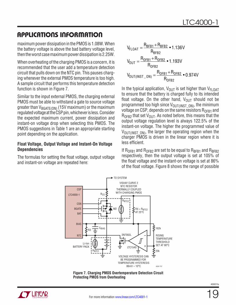
When overheating of the charging PMOS is a concern, it is recommended that the user add a temperature detection circuit that pulls down on the NTC pin. This pauses charg-ing whenever the external PMOS temperature is too high. A sample circuit that performs this temperature detection function is shown in Figure 7.
Similar to the input external PMOS, the charging external PMOS must be able to withstand a gate to source voltage greater than VBGATE(ON) (15V maximum) or the maximum regulated voltage at the CSP pin, whichever is less. Consider the expected maximum current, power dissipation and instant-on voltage drop when selecting this PMOS. The PMOS suggestions in Table 1 are an appropriate starting point depending on the application.
Float Voltage, Output Voltage and Instant-On Voltage Dependencies
The formulas for setting the float voltage, output voltage and instant-on voltage are repeated here:
Figure 7. Charging PMOS Overtemperature Detection Circuit Protecting PMOS from Overheating
applicaTions inForMaTion
VFLOAT = RBFB1 +RBFB2
RBFB2• 1.136V
VOUT = ROFB1 +ROFB2
ROFB2• 1.193V
VOUT(INST _ ON) = ROFB1 +ROFB2
ROFB2• 0.974V
In the typical application, VOUT is set higher than VFLOAT to ensure that the battery is charged fully to its intended float voltage. On the other hand, VOUT should not be programmed too high since VOUT(INST_ON), the minimum voltage on CSP, depends on the same resistors ROFB1 and ROFB2 that set VOUT. As noted before, this means that the output voltage regulation level is always 122.5% of the instant-on voltage. The higher the programmed value of VOUT(INST_ON), the larger the operating region when the charger PMOS is driven in the linear region where it is less efficient.
If ROFB1 and ROFB2 are set to be equal to RBFB1 and RBFB2 respectively, then the output voltage is set at 105% of the float voltage and the instant-on voltage is set at 86% of the float voltage. Figure 8 shows the range of possible
Li-IonBATTERY PACK
RCS
M2
RNTC1
TO SYSTEM
RISING TEMPERATURETHRESHOLD SET AT 90°C
VISHAY CURVE 2NTC RESISTOR
THERMALLY COUPLEDWITH CHARGING PMOS
VOLTAGE HYSTERESIS CANBE PROGRAMMED FOR
TEMPERATURE HYSTERESIS86mV ≈ 10°C
CSN
BGATE
BAT
CSP
BIAS
NTC
LTC4000-1
162k
20k
R3
R4 = RNTC2AT 25°C
40001 F07
CBIAS
RNTC2
LTC1540 +
–2N7002L
LTC4000-1
2040001fa
For more information www.linear.com/LTC4001-1
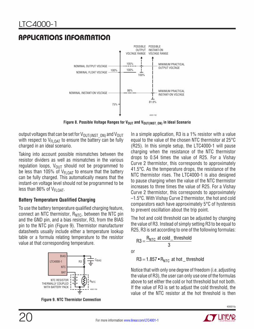
Figure 8. Possible Voltage Ranges for VOUT and VOUT(INST_ON) in Ideal Scenario
NOMINAL OUTPUT VOLTAGE
POSSIBLEOUTPUT
VOLTAGE RANGE
75%
86%
40001 F08
POSSIBLEINSTANT-ONVOLTAGE RANGE
105%
100%
100%
81.6%
NOMINAL FLOAT VOLTAGE100%
NOMINAL INSTANT-ON VOLTAGE
MINIMUM PRACTICALOUTPUT VOLTAGE
MINIMUM PRACTICALINSTANT-ON VOLTAGE
applicaTions inForMaTion
output voltages that can be set for VOUT(INST_ON) and VOUT with respect to VFLOAT to ensure the battery can be fully charged in an ideal scenario.
Taking into account possible mismatches between the resistor dividers as well as mismatches in the various regulation loops, VOUT should not be programmed to be less than 105% of VFLOAT to ensure that the battery can be fully charged. This automatically means that the instant-on voltage level should not be programmed to be less than 86% of VFLOAT.
Battery Temperature Qualified Charging
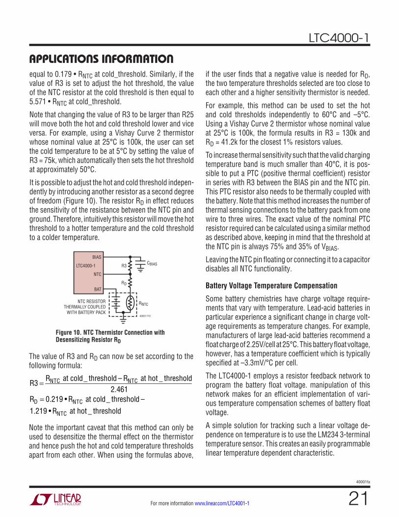
To use the battery temperature qualified charging feature, connect an NTC thermistor, RNTC, between the NTC pin and the GND pin, and a bias resistor, R3, from the BIAS pin to the NTC pin (Figure 9). Thermistor manufacturer datasheets usually include either a temperature lookup table or a formula relating temperature to the resistor value at that corresponding temperature.
Figure 9. NTC Thermistor Connection
NTC RESISTORTHERMALLY COUPLED
WITH BATTERY PACK
R3
RNTC
NTC
BIAS
BAT
LTC4000-1
40001 F09
CBIAS
In a simple application, R3 is a 1% resistor with a value equal to the value of the chosen NTC thermistor at 25°C (R25). In this simple setup, the LTC4000-1 will pause charging when the resistance of the NTC thermistor drops to 0.54 times the value of R25. For a Vishay Curve 2 thermistor, this corresponds to approximately 41.5°C. As the temperature drops, the resistance of the NTC thermistor rises. The LTC4000-1 is also designed to pause charging when the value of the NTC thermistor increases to three times the value of R25. For a Vishay Curve 2 thermistor, this corresponds to approximately –1.5°C. With Vishay Curve 2 thermistor, the hot and cold comparators each have approximately 5°C of hysteresis to prevent oscillation about the trip point.
The hot and cold threshold can be adjusted by changing the value of R3. Instead of simply setting R3 to be equal to R25, R3 is set according to one of the following formulas:
R3 = RNTC at cold_ threshold
3or
R3 = 1.857 • RNTC at hot _ threshold
Notice that with only one degree of freedom (i.e. adjusting the value of R3), the user can only use one of the formulas above to set either the cold or hot threshold but not both. If the value of R3 is set to adjust the cold threshold, the value of the NTC resistor at the hot threshold is then
LTC4000-1
2140001fa
For more information www.linear.com/LTC4001-1
applicaTions inForMaTionif the user finds that a negative value is needed for RD, the two temperature thresholds selected are too close to each other and a higher sensitivity thermistor is needed.
For example, this method can be used to set the hot and cold thresholds independently to 60°C and –5°C. Using a Vishay Curve 2 thermistor whose nominal value at 25°C is 100k, the formula results in R3 = 130k and RD = 41.2k for the closest 1% resistors values.
To increase thermal sensitivity such that the valid charging temperature band is much smaller than 40°C, it is pos-sible to put a PTC (positive thermal coefficient) resistor in series with R3 between the BIAS pin and the NTC pin. This PTC resistor also needs to be thermally coupled with the battery. Note that this method increases the number of thermal sensing connections to the battery pack from one wire to three wires. The exact value of the nominal PTC resistor required can be calculated using a similar method as described above, keeping in mind that the threshold at the NTC pin is always 75% and 35% of VBIAS.
Leaving the NTC pin floating or connecting it to a capacitor disables all NTC functionality.
Battery Voltage Temperature Compensation
Some battery chemistries have charge voltage require-ments that vary with temperature. Lead-acid batteries in particular experience a significant change in charge volt-age requirements as temperature changes. For example, manufacturers of large lead-acid batteries recommend a float charge of 2.25V/cell at 25°C. This battery float voltage, however, has a temperature coefficient which is typically specified at –3.3mV/°C per cell.
The LTC4000-1 employs a resistor feedback network to program the battery float voltage. manipulation of this network makes for an efficient implementation of vari-ous temperature compensation schemes of battery float voltage.
A simple solution for tracking such a linear voltage de-pendence on temperature is to use the LM234 3-terminal temperature sensor. This creates an easily programmable linear temperature dependent characteristic.
equal to 0.179 • RNTC at cold_threshold. Similarly, if the value of R3 is set to adjust the hot threshold, the value of the NTC resistor at the cold threshold is then equal to 5.571 • RNTC at cold_threshold.
Note that changing the value of R3 to be larger than R25 will move both the hot and cold threshold lower and vice versa. For example, using a Vishay Curve 2 thermistor whose nominal value at 25°C is 100k, the user can set the cold temperature to be at 5°C by setting the value of R3 = 75k, which automatically then sets the hot threshold at approximately 50°C.
It is possible to adjust the hot and cold threshold indepen-dently by introducing another resistor as a second degree of freedom (Figure 10). The resistor RD in effect reduces the sensitivity of the resistance between the NTC pin and ground. Therefore, intuitively this resistor will move the hot threshold to a hotter temperature and the cold threshold to a colder temperature.
Figure 10. NTC Thermistor Connection with Desensitizing Resistor RD
NTC RESISTORTHERMALLY COUPLED
WITH BATTERY PACK
R3
RNTC
NTC
BIAS
BAT
LTC4000-1
RD
40001 F10
CBIAS
The value of R3 and RD can now be set according to the following formula:
R3 = RNTC at cold_ threshold – RNTC at hot _ threshold2.461
RD = 0.219 • RNTC at cold_ threshold –1.219 • RNTC at hot _ threshold
Note the important caveat that this method can only be used to desensitize the thermal effect on the thermistor and hence push the hot and cold temperature thresholds apart from each other. When using the formulas above,
LTC4000-1
2240001fa
For more information www.linear.com/LTC4001-1
applicaTions inForMaTion
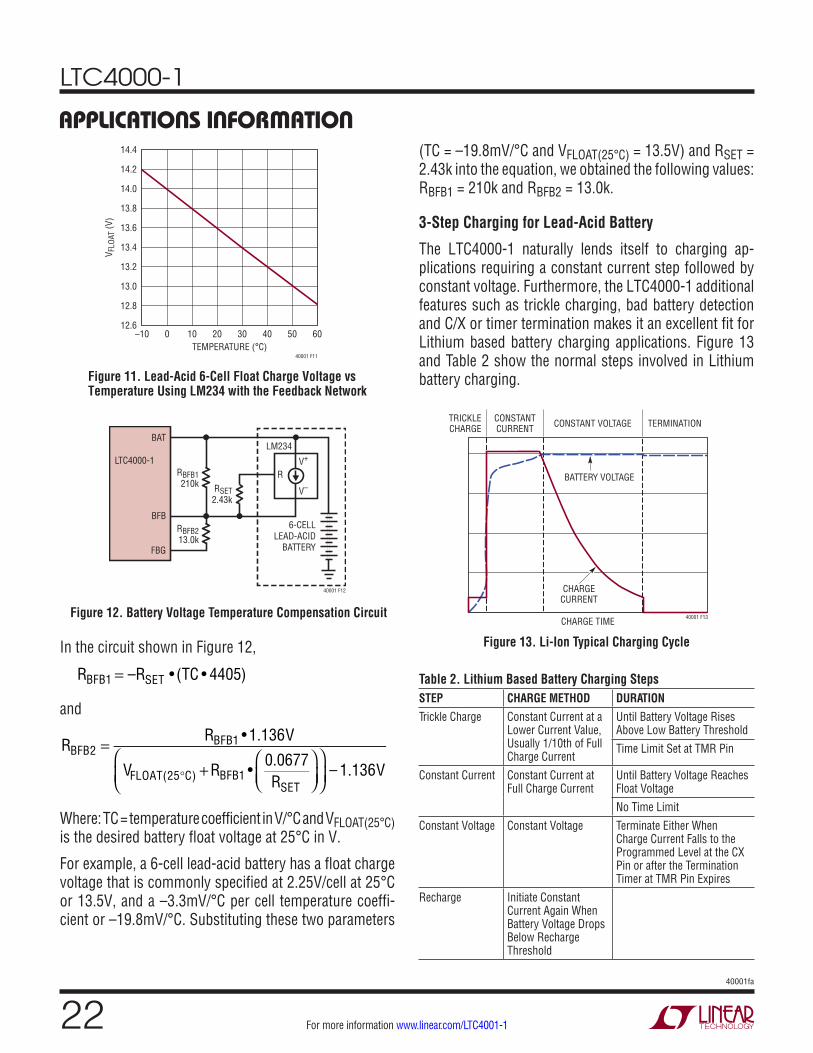
In the circuit shown in Figure 12,
RBFB1 = –RSET • (TC • 4405)
and
RBFB2 = RBFB1 • 1.136V
VFLOAT(25°C) + RBFB1 •0.0677RSET
– 1.136V
Where: TC = temperature coefficient in V/°C and VFLOAT(25°C) is the desired battery float voltage at 25°C in V.
For example, a 6-cell lead-acid battery has a float charge voltage that is commonly specified at 2.25V/cell at 25°C or 13.5V, and a –3.3mV/°C per cell temperature coeffi-cient or –19.8mV/°C. Substituting these two parameters
(TC = –19.8mV/°C and VFLOAT(25°C) = 13.5V) and RSET = 2.43k into the equation, we obtained the following values: RBFB1 = 210k and RBFB2 = 13.0k.
3-Step Charging for Lead-Acid Battery
The LTC4000-1 naturally lends itself to charging ap-plications requiring a constant current step followed by constant voltage. Furthermore, the LTC4000-1 additional features such as trickle charging, bad battery detection and C/X or timer termination makes it an excellent fit for Lithium based battery charging applications. Figure 13 and Table 2 show the normal steps involved in Lithium battery charging.
Figure 13. Li-Ion Typical Charging Cycle
CHARGE TIME 40001 F13
CONSTANT VOLTAGECONSTANTCURRENT
TRICKLECHARGE
CHARGECURRENT
BATTERY VOLTAGE
TERMINATION
Figure 12. Battery Voltage Temperature Compensation Circuit
Figure 11. Lead-Acid 6-Cell Float Charge Voltage vs Temperature Using LM234 with the Feedback Network
TEMPERATURE (°C)–10
V FLO
AT (V
)
14.4
14.2
13.8
13.4
13.0
14.0
13.6
13.2
12.8
12.63010 50
40001 F11
60200 40
RBFB1210k
RBFB213.0k
BFB
R
LM234
V+
V–
BAT
FBG
LTC4000-1
RSET2.43k
40001 F12
6-CELLLEAD-ACID
BATTERY
Table 2. Lithium Based Battery Charging StepsSTEP CHARGE METHOD DURATIONTrickle Charge Constant Current at a
Lower Current Value, Usually 1/10th of Full Charge Current
Until Battery Voltage Rises Above Low Battery Threshold
Time Limit Set at TMR Pin
Constant Current Constant Current at Full Charge Current
Until Battery Voltage Reaches Float Voltage
No Time Limit
Constant Voltage Constant Voltage Terminate Either When Charge Current Falls to the Programmed Level at the CX Pin or after the Termination Timer at TMR Pin Expires
Recharge Initiate Constant Current Again When Battery Voltage Drops Below Recharge Threshold
LTC4000-1
2340001fa
For more information www.linear.com/LTC4001-1
applicaTions inForMaTionOn the other hand, the LTC4000-1 is also easily configu-rable to handle lead-acid based battery charging. One of the common methods used in lead-acid battery charging is called 3-step charging (Bulk, Absorption and Float). Figure 14 and Table 3 summarize the normal steps involved in a typical 3-step charging of a lead-acid battery.
Figure 14. Lead-Acid 3-Step Charging Cycle
Figure 15. 3-Step Lead-Acid Circuit Configuration
CHARGE TIME 40001 F14
FLOAT(STORAGE)
BULKCHARGE
CHARGECURRENT
BATTERY VOLTAGE
ABSORPTION
RBFB2
RBFB3
BFB
CSP
CX CHRG
FBG
LTC4000-1
CSN
BAT
RCS
RCX
CL
RCL
RBFB1
40001 F15
LEAD-ACIDBATTERY
FROM DC/DCOUTPUT
When a charging cycle is initiated, the CHRG pin is pulled low. The charger first enters the bulk charge step, charg-ing the battery with a constant current programmed at the CL pin:
ICLIM =
MIN 50mV, 2.5µA •RCL( )RCS
When the battery voltage rises to the Absorption voltage level:
VABSRP =
RBFB1 RBFB2 + RBFB3( )RBFB2RBFB3
+ 1
• 1.136V
the charger enters the Absorption step, charging the bat-tery at a constant voltage at this absorption voltage level.
As the charge current drops to the C/X level:
ICLIM =
0.25µA •RCX( ) – 0.5mVRCS
the CHRG pin turns high impedance and now the charger enters the Float (Storage) step, charging the battery volt-age at the constant float voltage level:
VFLOAT = RBFB1
RBFB2+ 1
• 1.136V
Table 3. Lead-Acid Battery Charging StepsSTEP CHARGE METHOD DURATION
Bulk Charge Constant Current Until Battery Voltage Reaches Absorption Voltage
No Time Limit
Absorption Constant Voltage at the Absorption Voltage Level
Terminate When Charge Current Falls to the Programmed Level at the CX Pin
Float (Storage) Constant Voltage at the Lower Float Voltage Level (Float Voltage Is Lower than the Absorption Voltage)
Indefinite
Recharge Initiate Bulk Charge Again When Battery Voltage Drops Below Recharge Threshold
Figure 15 shows the configuration needed to implement this 3-step lead-acid battery charging with the LTC4000-1.

LTC4000-1
2440001fa
For more information www.linear.com/LTC4001-1
applicaTions inForMaTionNote that in this configuration, the recharge threshold is 97.6% of the float voltage level. When the battery voltage drops below this level, the whole 3-step charging cycle is reinitiated starting with the bulk charge.
Some systems require trickle charging of an over dis-charged lead-acid battery. This feature can be included using the CL pin of the LTC4000-1. In the configuration shown in Figure 15, when the battery voltage is lower than 68% of the Absorption level, the pull-up current on the CL pin is reduced to 10% of the normal pull-up cur-rent. Therefore, the trickle charge current can be set at the following level:
ICLIM =
MIN 50mV, 0.25µA •RCL( )RCS
If this feature is not desired, leave the CL pin open to set the regulation voltage across the charge current sense resistor (RCS) always at 50mV.
The FLT and CHRG Indicator Pins
The FLT and CHRG pins in the LTC4000-1 provide status indicators. Table 4 summarizes the mapping of the pin states to the part status.
Table 4. FLT and CHRG Status IndicatorFLT CHRG STATUS
0 0 NTC Over Ranged – Charging Paused
1 0 Charging Normally
0 1 Charging Terminated and Bad Battery Detected
1 1 VIBMON < (VC/X – 10mV)
where 1 indicates a high impedance state and 0 indicates a low impedance pull-down state.
Note that VIBMON < (VCX – 10mV) corresponds to charge termination only if the C/X termination is selected. If the charger timer termination is selected, constant voltage charging may continue for the remaining charger timer period even after the indicator pins indicate that VIBMON < (VCX – 10mV). This is also true when no termination is selected, constant voltage charging will continue even after the indicator pins indicate that VIBMON < (VCX – 10mV).
The BIAS Pin
For ease of use the LTC4000-1 provides a low dropout voltage regulator output on the BIAS pin. Designed to provide up to 0.5mA of current at 2.9V, this pin requires at least 470nF of low ESR bypass capacitance for stability.
Use the BIAS pin as the pull-up source for the NTC resis-tor networks, since the internal reference for the NTC circuitry is based on a ratio of the voltage on the BIAS pin. Furthermore, various 100k pull-up resistors can be conveniently connected to the BIAS pin.
Setting the Input Voltage Monitoring Resistor Divider
The falling threshold voltage level for this monitoring function can be calculated as follows:
RVM1 =
VVM _RST
1.193V– 1
• RVM2
where RVM1 and RVM2 form a resistor divider connected between the monitored voltage and GND, with the center tap point connected to the VM pin as shown in Figure 6. The rising threshold voltage level can be calculated similarly.
Input Voltage Programming
Connecting a resistor divider from VIN to the IFB pin en-ables programming of a minimum input supply voltage. This feature is typically used to program the peak power voltage for a high impedance input source. Referring to Figure 2, the input voltage regulation level is determined using the following formula:
RIFB1 =
VIN _REG
1V– 1
RIFB2
Where VIN_REG is the minimum regulation input voltage level, below which the current draw from the input source is reduced.
Combining the Input Voltage Programming and the Input Voltage Monitoring Resistor Divider
When connected to the same input voltage node, the input voltage monitoring and the input voltage regulation resistor divider can be combined (see Figure 16).
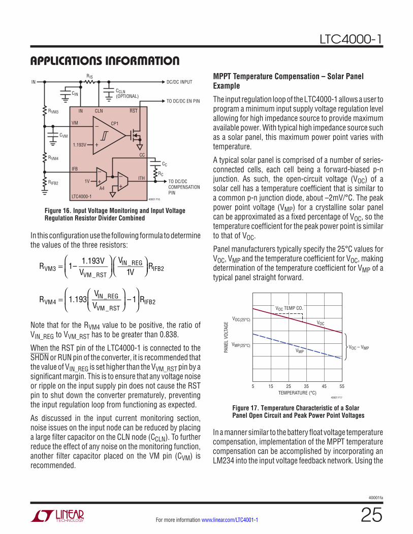
LTC4000-1
2540001fa
For more information www.linear.com/LTC4001-1
In this configuration use the following formula to determine the values of the three resistors:
RVM3 = 1–
1.193VVVM _RST
VIN _REG
1V
RIFB2
RVM4 = 1.193
VIN _REG
VVM _RST
– 1
RIFB2
Note that for the RVM4 value to be positive, the ratio of VIN_REG to VVM_RST has to be greater than 0.838.
When the RST pin of the LTC4000-1 is connected to the SHDN or RUN pin of the converter, it is recommended that the value of VIN_REG is set higher than the VVM_RST pin by a significant margin. This is to ensure that any voltage noise or ripple on the input supply pin does not cause the RST pin to shut down the converter prematurely, preventing the input regulation loop from functioning as expected.
As discussed in the input current monitoring section, noise issues on the input node can be reduced by placing a large filter capacitor on the CLN node (CCLN). To further reduce the effect of any noise on the monitoring function, another filter capacitor placed on the VM pin (CVM) is recommended.
MPPT Temperature Compensation – Solar Panel Example
The input regulation loop of the LTC4000-1 allows a user to program a minimum input supply voltage regulation level allowing for high impedance source to provide maximum available power. With typical high impedance source such as a solar panel, this maximum power point varies with temperature.
A typical solar panel is comprised of a number of series-connected cells, each cell being a forward-biased p-n junction. As such, the open-circuit voltage (VOC) of a solar cell has a temperature coefficient that is similar to a common p-n junction diode, about –2mV/°C. The peak power point voltage (VMP) for a crystalline solar panel can be approximated as a fixed percentage of VOC, so the temperature coefficient for the peak power point is similar to that of VOC.
Panel manufacturers typically specify the 25°C values for VOC, VMP and the temperature coefficient for VOC, making determination of the temperature coefficient for VMP of a typical panel straight forward.
applicaTions inForMaTion
IN
CC
1VITH
LTC4000-1
IN CLN RST
RISDC/DC INPUT
TO DC/DC EN PIN
CCLN(OPTIONAL)
CVM
IFB
VM
CIN
–+
–+
CC
TO DC/DCCOMPENSATIONPIN
40001 F16
RC
A4RIFB2
RVM4
RVM3
CP1
+
–
1.193V
Figure 16. Input Voltage Monitoring and Input Voltage Regulation Resistor Divider Combined
Figure 17. Temperature Characteristic of a Solar Panel Open Circuit and Peak Power Point Voltages
TEMPERATURE (°C)5
PANE
L VO
LTAG
E
VOC(25°C)
VOC – VMPVMP(25°C)
4525
40001 F17
553515
VMP
VOC
VOC TEMP CO.
In a manner similar to the battery float voltage temperature compensation, implementation of the MPPT temperature compensation can be accomplished by incorporating an LM234 into the input voltage feedback network. Using the

LTC4000-1
2640001fa
For more information www.linear.com/LTC4001-1
feedback network in Figure 18, a similar set of equations can be used to determine the resistor values:
RIFB1 = –RSET • (TC • 4405)
and
RIFB2 = RIFB1 • 1V
VMP(25°C) + RIFB1 •0.0677RSET
– 1V
Where: TC = temperature coefficient in V/°C, and VMP(25°C) = maximum power point voltage at 25°C in V.
typical sinking capability of the LTC4000-1 at the ITH pin is 1mA at 0.4V with a maximum voltage range of 0V to 6V.
It is imperative that the local feedback of the DC/DC con-verter be set up such that during regulation of any of the LTC4000-1 loops this local loop is out of regulation and sources as much current as possible from its ITH/VC pin. For example for a DC/DC converter regulating its output voltage, it is recommended that the converter feedback divider is programmed to be greater than 110% of the output voltage regulation level programmed at the OFB pin.
There are four feedback loops to consider when setting up the compensation for the LTC4000-1. As mentioned before these loops are: the input voltage loop, the charge current loop, the float voltage loop and the output volt-age loop. All of these loops have an error amp (A4-A7) followed by another amplifier (A10) with the intermediate node driving the CC pin and the output of A10 driving the ITH pin as shown in Figure 19. The most common com-pensation network of a series capacitor (CC) and resistor (RC) between the CC pin and the ITH pin is shown here.
Each of the loops has slightly different dynamics due to differences in the feedback signal path. The analytic de-scription of the input voltage regulation loop is included in the Appendix section. Please refer to the LTC4000 data sheet for the analytic description of the other three loops. In most situations, an alternative empirical approach to compensation, as described here, is more practical.
applicaTions inForMaTion
Figure 18. Maximum Power Point Voltage Temperature Compensation Feedback Network
RIFB1348k
RIFB28.66k
IFB
R
LM234
V+
V–
INVIN
LTC4000-1
RSET1k
40001 F18
Figure 19. Error Amplifier Followed by Output Amplifier Driving CC and ITH Pins
CC
ITH
LTC4000-1
–+
CC
40001 F11
RC
A4-A7gm4-7 = 0.2m A10
gm10 = 0.1m+–
RO4-7RO10
For example, given a common 36-cell solar panel that has the following specified characteristics:
Open circuit voltage (VOC) = 21.7V
Maximum power voltage (VMP) = 17.6V
Open-circuit voltage temperature coefficient (VOC) = –78mV/°C
As the temperature coefficient for VMP is similar to that of VOC, the specified temperature coefficient for VOC (TC) of –78mV/°C and the specified peak power voltage (VMP(25°C)) of 17.6V can be inserted into the equations to calculate the appropriate resistor values for the temperature compensa-tion network in Figure 18. With RSET equal to 1kΩ, then:
RSET = 1kΩ, RIFB1 = 348kΩ, RIFB2 = 8.66kΩ.
Compensation
In order for the LTC4000-1 to control the external DC/DC converter, it has to be able to overcome the sourcing bias current of the ITH or VC pin of the DC/DC converter. The
Empirical Loop Compensation
Based on the analytical expressions and the transfer function from the ITH pin to the input and output current of the external DC/DC converter, the user can analytically

LTC4000-1
2740001fa
For more information www.linear.com/LTC4001-1
applicaTions inForMaTiondetermine the complete loop transfer function of each of the loops. Once these are obtained, it is a matter of analyz-ing the gain and phase bode plots to ensure that there is enough phase and gain margin at unity crossover with the selected values of RC and CC for all operating conditions.
Even though it is clear that an analytical compensation method is possible, sometimes certain complications render this method difficult to tackle. These complica-tions include the lack of easy availability of the switching converter transfer function from the ITH or VC control node to its input or output current, and the variability of parameter values of the components such as the ESR of the output capacitor or the RDS(ON) of the external PFETs.
Therefore a simpler and more practical way to compensate the LTC4000-1 is provided here. This empirical method involves injecting an AC signal into the loop, observing the loop transient response and adjusting the CC and RC values to quickly iterate towards the final values. Much of the detail of this method is derived from Application Note 19 which can be found at www.linear.com using AN19 in the search box.
Figure 20 shows the recommended setup to inject an AC-coupled output load variation into the loop. A function generator with 50Ω output impedance is coupled through a 50Ω/1000µF series RC network to the regulator output. Generator frequency is set at 50Hz. Lower frequencies
may cause a blinking scope display and higher frequen-cies may not allow sufficient settling time for the output transient. Amplitude of the generator output is typically set at 5VP-P to generate a 100mAP-P load variation. For lightly loaded outputs (IOUT < 100mA), this level may be too high for small signal response. If the positive and negative transition settling waveforms are significantly different, amplitude should be reduced. Actual amplitude is not particularly important because it is the shape of the resulting regulator output waveform which indicates loop stability.
A 2-pole oscilloscope filter with f = 10kHz is used to block switching frequencies. Regulators without added LC output filters have switching frequency signals at their outputs which may be much higher amplitude than the low frequency settling waveform to be studied. The filter frequency is high enough for most applications to pass the settling waveform with no distortion.
Oscilloscope and generator connections should be made exactly as shown in Figure 20 to prevent ground loop er-rors. The oscilloscope is synced by connecting the chan-nel B probe to the generator output, with the ground clip of the second probe connected to exactly the same place as channel A ground. The standard 50Ω BNC sync output of the generator should not be used because of ground loop errors. It may also be necessary to isolate either the generator or oscilloscope from its third wire (earth
Figure 20. Empirical Loop Compensation Setup
IOUT
VIN
CSN
CSP
IN
CLN
BATGND
LTC4000-1
50Ω1W
50ΩGENERATORf = 50Hz
RCITHGND
SWITCHINGCONVERTER
40001 F20
BGATE
ITH CC
CC
1000µF(OBSERVEPOLARITY)
SCOPEGROUNDCLIP
10k A1k
1500pF0.015µF
B
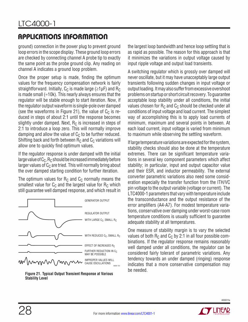
LTC4000-1
2840001fa
For more information www.linear.com/LTC4001-1
applicaTions inForMaTionground) connection in the power plug to prevent ground loop errors in the scope display. These ground loop errors are checked by connecting channel A probe tip to exactly the same point as the probe ground clip. Any reading on channel A indicates a ground loop problem.
Once the proper setup is made, finding the optimum values for the frequency compensation network is fairly straightforward. Initially, CC is made large (≥1μF) and RC is made small (≈10k). This nearly always ensures that the regulator will be stable enough to start iteration. Now, if the regulator output waveform is single-pole over damped (see the waveforms in Figure 21), the value of CC is re-duced in steps of about 2:1 until the response becomes slightly under damped. Next, RC is increased in steps of 2:1 to introduce a loop zero. This will normally improve damping and allow the value of CC to be further reduced. Shifting back and forth between RC and CC variations will allow one to quickly find optimum values.
If the regulator response is under damped with the initial large value of CC, RC should be increased immediately before larger values of CC are tried. This will normally bring about the over damped starting condition for further iteration.
The optimum values for RC and CC normally means the smallest value for CC and the largest value for RC which still guarantee well damped response, and which result in
the largest loop bandwidth and hence loop settling that is as rapid as possible. The reason for this approach is that it minimizes the variations in output voltage caused by input ripple voltage and output load transients.
A switching regulator which is grossly over damped will never oscillate, but it may have unacceptably large output transients following sudden changes in input voltage or output loading. It may also suffer from excessive overshoot problems on startup or short circuit recovery. To guarantee acceptable loop stability under all conditions, the initial values chosen for RC and CC should be checked under all conditions of input voltage and load current. The simplest way of accomplishing this is to apply load currents of minimum, maximum and several points in between. At each load current, input voltage is varied from minimum to maximum while observing the settling waveform.
If large temperature variations are expected for the system, stability checks should also be done at the temperature extremes. There can be significant temperature varia-tions in several key component parameters which affect stability; in particular, input and output capacitor value and their ESR, and inductor permeability. The external converter parametric variations also need some consid-eration especially the transfer function from the ITH/VC pin voltage to the output variable (voltage or current). The LTC4000-1 parameters that vary with temperature include the transconductance and the output resistance of the error amplifiers (A4-A7). For modest temperature varia-tions, conservative over damping under worst-case room temperature conditions is usually sufficient to guarantee adequate stability at all temperatures.
One measure of stability margin is to vary the selected values of both RC and CC by 2:1 in all four possible com-binations. If the regulator response remains reasonably well damped under all conditions, the regulator can be considered fairly tolerant of parametric variations. Any tendency towards an under damped (ringing) response indicates that a more conservative compensation may be needed.
Figure 21. Typical Output Transient Response at Various Stability Level
GENERATOR OUTPUT
REGULATOR OUTPUT
WITH LARGE CC, SMALL RC
WITH REDUCED CC, SMALL RC
FURTHER REDUCTION IN CC MAY BE POSSIBLE
IMPROPER VALUES WILL CAUSE OSCILLATIONS
EFFECT OF INCREASED RC
40001 F21

LTC4000-1
2940001fa
For more information www.linear.com/LTC4001-1
applicaTions inForMaTionDESIGN EXAMPLE
In this design example, the LTC4000-1 is paired with the LT3845A buck converter to create a 10A, 3-cell LiFePO4 battery charger. The circuit is shown on the front page and is repeated here in Figure 22.
• With RIFB2 set at 20k, the input voltage monitoring falling threshold is set at 15V and the input voltage regulation level is set at 17.6V according to the following formulas:
RVM3 = 1− 1.193V
15V
17.6V1V
20kΩ = 324kΩ
RVM4 = 1.193V
17.6V15V
− 1
20kΩ = 8.06kΩ
• The input current sense resistor is set at 5mΩ. There-fore, the voltage at the IIMON pin is related to the input current according to the following formula:
VIIMON = (0.1Ω) • IRIS
• RCL is set at 24.9kΩ such that the voltage at the CL pin is 1.25V. Similar to the IIMON pin, the regulation voltage on the IBMON pin is clamped at 1V with an accurate internal reference. Therefore, the charge current limit is set at 10A according to the following formula:
ICLIM(MAX) = 0.050V
RCS= 0.050V
5mΩ= 10A
• The trickle charge current level is consequently set at 1.25A, according to the following formula:
ICLIM(TRKL) = 0.25µA • 24.9kΩ
5mΩ= 1.25A
• The battery float voltage is set at 10.8V according to the following formula:
RBFB1 = 10.8
1.136− 1
• 133kΩ ≈ 1.13MΩ
Figure 22. 10.8V at 10A Charger for Three LiFePO4 Cells with Solar Panel Input
1.13M
14.7k
127k
10k10k 3-CELL Li-Ion
BATTERY PACK
VBAT10.8V FLOAT10A MAX CHARGECURRENT
NTHS0603N02N1002J
1.15M47nF
5mΩ
VOUT12V, 15A
SOLAR PANEL INPUT<60V OPEN CIRCUIT VOLTAGE17.6V PEAK POWER VOLTAGE
133k
CSNCSP
BGATE
IGATE
BAT
OFB
FBG
BFB
NTC
CX
LTC4000-1
ITH CC IID
5mΩ LT3845A
100µF
OUTVCSHDN
IN
RSTCLNIN
ENCCHRGFLT
VM
22.1k
CLTMRIIMON IBMON
BIAS
GND BIAS
BIAS
24.9k
1µF324k
8.06k
IFB
20k
1µF10nF
40001 F22
Si7135DP
Si7135DP
3.0V
1M
0.1µF
10nF
10M

LTC4000-1
3040001fa
For more information www.linear.com/LTC4001-1
Figure 23. Charge Current Regulation Loop Compensation Setup
LTC4000-1
10k 1k
40001 F23
0.015µF
SQUARE WAVEGENERATORf = 60Hz
IBMON
CL
1500pF
B A
• The bad battery detection time is set at 43 minutes according to the following formula:
CTMR(nF) = tBADBAT(h) • 138.5 = 43
60• 138.5 = 100nF
• The charge termination time is set at 2.9 hours accord-ing to the following formula:
CTMR(nF) = tTERMINATE(h) • 34.6 = 2.9 • 34.6 = 100nF
• The C/X current termination level is programmed at 1A according to the following formula:
RCX =
1A • 5mΩ( ) + 0.5mV0.25µA
≈ 22.1kΩ
Note that in this particular solution, the timer termina-tion is selected since a capacitor connects to the TMR pin. Therefore, this C/X current termination level only applies to the CHRG indicator pin.
• The output voltage regulation level is set at 12V accord-ing to the following formula:
ROFB1 = 12
1.193− 1
• 127kΩ ≈ 1.15MΩ
• The instant-on voltage level is consequently set at 9.79V according to the following formula:
VINST _ ON = 1150kΩ + 127kΩ
127kΩ• 0.974V = 9.79V
The worst-case power dissipation during instant-on operation can be calculated as follows:
• During trickle charging:
PTRKL = 0.86 • VFLOAT – VBAT[ ] • ICLIM _ TRKL
= 0.86 • 10.8[ ] • 1A
= 9.3W
• And beyond trickle charging:
PINST _ ON = 0.86 • VFLOAT – VBAT[ ] • ICLIM
= 0.86 • 10.8 – 7.33[ ] • 10A
= 19.3W
Therefore, depending on the layout and heat sink avail-able to the charging PMOS, the suggested PMOS over temperature detection circuit included in Figure 7 may need to be included.
• The range of valid temperature for charging is set at –1.5°C to 41.5°C by picking a 10k Vishay Curve 2 NTC thermistor that is thermally coupled to the battery, and connecting this in series with a regular 10k resistor to the BIAS pin.
• For compensation, the procedure described in the empirical loop compensation section is followed. As recommended, first a 1µF CC and 10k RC is used, which sets all the loops to be stable. For an example of typical transient responses, the charge current regulation loop when VOFB is regulated to VOUT(INST_ON) is used here. Figure 23 shows the recommended setup to inject a DC-coupled charge current variation into this particular loop. The input to the CL pin is a square wave at 70Hz with the low level set at 120mV and the high level set at 130mV, corresponding to a 1.2A and 1.3A charge current (100mA charge current step). Therefore, in this particular example the trickle charge current regulation stability is examined. Note that the nominal trickle charge current in this example is programmed at 1.25A (RCL = 24.9kΩ).
applicaTions inForMaTion

LTC4000-1
3140001fa
For more information www.linear.com/LTC4001-1
applicaTions inForMaTion With CC = 1µF, RC = 10k at VIN = 20V, VBAT = 7V, VCSP
regulated at 9.8V and a 0.2A output load condition at CSP, the transient response for a 100mA charge current step observed at IBMON is shown in Figure 24.
The transient response now indicates an overall under damped system. As noted in the empirical loop compensa-tion section, the value of RC is now increased iteratively until RC = 20k. The transient response of the same loop with CC = 22nF and RC = 20k is shown in Figure 26.
Figure 24. Transient Response of Charge Current Regulation Loop Observed at IBMON When VOFB is Regulated to VOUT(INST_ON) with CC = 1µF, RC = 10k for a 100mA Charge Current Step
5ms/DIV–20
V IBM
ON (m
V)5m
V/DI
V
15
–10
–5
0
5
10
–15105 15
40001 F24
25200–10 –5–15
The transient response shows a small overshoot with slow settling indicating a fast minor loop within a well damped overall loop. Therefore, the value of CC is reduced iteratively until CC = 22nF. The transient response of the same loop with CC = 22nF and RC = 10k is shown in Figure 25.
Figure 25. Transient Response of Charge Current Regulation Loop Observed at IBMON When VOFB is Regulated to VOUT(INST_ON) with CC = 22nF, RC = 10k for a 100mA Charge Current Step
Figure 26. Transient Response of Charge Current Regulation Loop Observed at IBMON When VOFB is Regulated to VOUT(INST_ON) with CC = 22nF, RC = 20k for a 100mA Charge Current Step
5ms/DIV–20
V IBM
ON (m
V)5m
V/DI
V
15
–10
–5
0
5
10
–15105 15
40001 F25
25200–10 –5–15
5ms/DIV–20
V IBM
ON (m
V)5m
V/DI
V
15
–10
–5
0
5
10
–15105 15
40001 F26
25200–10 –5–15
Note that the transient response is close to optimum with some overshoot and fast settling. If after iteratively increasing the value of RC, the transient response again indicates an over damped system, the step of reducing CC can be repeated. These steps of reducing CC followed by increasing RC can be repeated continuously until one arrives at a stable loop with the smallest value of CC and the largest value of RC. In this particular example, these values are found to be CC = 22nF and RC = 20kΩ.
After arriving at these final values of RC and CC, the stability margin is checked by varying the values of both RC and CC by 2:1 in all four possible combinations. After which the setup condition is varied, including varying the input voltage level and the output load level and the transient response is checked at these different setup conditions. Once the desired responses on all different conditions are obtained, the values of RC and CC are noted.
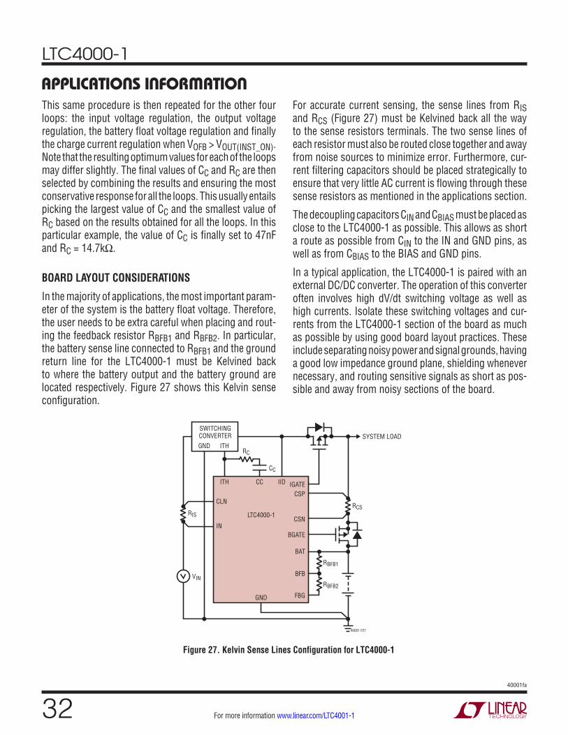
LTC4000-1
3240001fa
For more information www.linear.com/LTC4001-1
applicaTions inForMaTionThis same procedure is then repeated for the other four loops: the input voltage regulation, the output voltage regulation, the battery float voltage regulation and finally the charge current regulation when VOFB > VOUT(INST_ON). Note that the resulting optimum values for each of the loops may differ slightly. The final values of CC and RC are then selected by combining the results and ensuring the most conservative response for all the loops. This usually entails picking the largest value of CC and the smallest value of RC based on the results obtained for all the loops. In this particular example, the value of CC is finally set to 47nF and RC = 14.7kΩ.
BOARD LAYOUT CONSIDERATIONS
In the majority of applications, the most important param-eter of the system is the battery float voltage. Therefore, the user needs to be extra careful when placing and rout-ing the feedback resistor RBFB1 and RBFB2. In particular, the battery sense line connected to RBFB1 and the ground return line for the LTC4000-1 must be Kelvined back to where the battery output and the battery ground are located respectively. Figure 27 shows this Kelvin sense configuration.
For accurate current sensing, the sense lines from RIS and RCS (Figure 27) must be Kelvined back all the way to the sense resistors terminals. The two sense lines of each resistor must also be routed close together and away from noise sources to minimize error. Furthermore, cur-rent filtering capacitors should be placed strategically to ensure that very little AC current is flowing through these sense resistors as mentioned in the applications section.
The decoupling capacitors CIN and CBIAS must be placed as close to the LTC4000-1 as possible. This allows as short a route as possible from CIN to the IN and GND pins, as well as from CBIAS to the BIAS and GND pins.
In a typical application, the LTC4000-1 is paired with an external DC/DC converter. The operation of this converter often involves high dV/dt switching voltage as well as high currents. Isolate these switching voltages and cur-rents from the LTC4000-1 section of the board as much as possible by using good board layout practices. These include separating noisy power and signal grounds, having a good low impedance ground plane, shielding whenever necessary, and routing sensitive signals as short as pos-sible and away from noisy sections of the board.
Figure 27. Kelvin Sense Lines Configuration for LTC4000-1
40001 F27
VIN
CSN
CLN
IN
CSP
BAT
GND
LTC4000-1
RCITHGND
SWITCHINGCONVERTER
BGATE
ITH IIDCC
CC
IGATE
RBFB1
RIS
RCS
RBFB2
BFB
FBG
SYSTEM LOAD
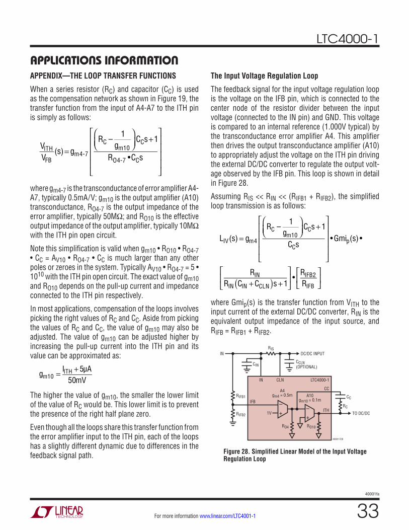
LTC4000-1
3340001fa
For more information www.linear.com/LTC4001-1
applicaTions inForMaTionAPPENDIX—THE LOOP TRANSFER FUNCTIONS
When a series resistor (RC) and capacitor (CC) is used as the compensation network as shown in Figure 19, the transfer function from the input of A4-A7 to the ITH pin is simply as follows:
VITHVFB
(s)= gm4-7
RC –1
gm10
CCs+1
RO4-7 •CCs
where gm4-7 is the transconductance of error amplifier A4-A7, typically 0.5mA/V; gm10 is the output amplifier (A10) transconductance, RO4-7 is the output impedance of the error amplifier, typically 50MΩ; and RO10 is the effective output impedance of the output amplifier, typically 10MΩ with the ITH pin open circuit.
Note this simplification is valid when gm10 • RO10 • RO4-7 • CC = AV10 • RO4-7 • CC is much larger than any other poles or zeroes in the system. Typically AV10 • RO4-7 = 5 • 1010 with the ITH pin open circuit. The exact value of gm10 and RO10 depends on the pull-up current and impedance connected to the ITH pin respectively.
In most applications, compensation of the loops involves picking the right values of RC and CC. Aside from picking the values of RC and CC, the value of gm10 may also be adjusted. The value of gm10 can be adjusted higher by increasing the pull-up current into the ITH pin and its value can be approximated as:
gm10 = IITH + 5µA
50mV
The higher the value of gm10, the smaller the lower limit of the value of RC would be. This lower limit is to prevent the presence of the right half plane zero.
Even though all the loops share this transfer function from the error amplifier input to the ITH pin, each of the loops has a slightly different dynamic due to differences in the feedback signal path.
The Input Voltage Regulation Loop
The feedback signal for the input voltage regulation loop is the voltage on the IFB pin, which is connected to the center node of the resistor divider between the input voltage (connected to the IN pin) and GND. This voltage is compared to an internal reference (1.000V typical) by the transconductance error amplifier A4. This amplifier then drives the output transconductance amplifier (A10) to appropriately adjust the voltage on the ITH pin driving the external DC/DC converter to regulate the output volt-age observed by the IFB pin. This loop is shown in detail in Figure 28.
Assuming RIS << RIN << (RIFB1 + RIFB2), the simplified loop transmission is as follows:
LIV(s) = gm4
RC –1
gm10
CCs + 1
CCs
• Gmip(s) •
RINRIN CIN + CCLN( )s + 1
•
RIFB2RIFB
where Gmip(s) is the transfer function from VITH to the input current of the external DC/DC converter, RIN is the equivalent output impedance of the input source, and RIFB = RIFB1 + RIFB2.
Figure 28. Simplified Linear Model of the Input Voltage Regulation Loop
IN
CC
1VITH
LTC4000-1IN CLN
RISDC/DC INPUT
CCLN(OPTIONAL)
IFB
CIN
–+
–+
CC
TO DC/DC
40001 F28
RC
RIFB2
RIFB1
A4gm4 = 0.5m A10
gm10 = 0.1m
RO4 RO10
LTC4000-1
3440001fa
For more information www.linear.com/LTC4001-1
Typical applicaTions
V–V+
LM23
4R 6-CE
LLLE
AD-A
CID
BATT
ERY
210k
14.7
k
Si71
35DP
47nF
15m
ΩV OUT
13.5
V
BSC1
23NO
8NS3
BAS5
21
1N41
48
B160
0.1µ
F
WÜR
TH E
LEKT
RONI
C74
4355
6110
010
µH
13.0
k
CSN
CSP
BGAT
E
IGAT
E
BAT
OFB
FBG
BFB
NTC
CX
LTC4
000-
1
ITH
BIAS
CCIID
442k
CHRG
2.4k
20m
Ω
3mΩ
LT38
45A SE
NSE+
BURS
T_EN
SENS
E–
33µF ×3
RST
CLN
IN
SW BG
BOOS
T
V CC
ENC
V FB
V CSH
DN
C SS
f SET
FLT
VM IFB
IIMON
IBM
ON
20k
CLTM
RGN
DBI
AS
BIAS
1µF
3.0V
1.10
M
100k
348k
10nF
10nF
10M
1µF
4000
1 F2
9
BSC1
23NO
8NS3
TG
182k
47µF
2.2µ
F
1µF 16
.2k
V IN
1.5n
F
49.9
k
SYNC
SGND
8.66
k
R
LM23
4
V+ V–
SOLA
R PA
NEL
INPU
T<4
0V O
PEN
CIRC
UIT
VOLT
AGE
17.6
V PE
AK P
OWER
VOL
TAGE
1k
Figu
re 2
9. S
olar
Pan
el In
put,
6-Ce
ll Le
ad-A
cid,
3-S
tep
Batte
ry C
harg
er w
ith 3
.3A
Bulk
Cha
rge
Curr
ent,
14.1
V at
25°
C Ab
sorp
tion
Volta
ge a
nd 1
3.5V
at
25°C
Flo
at V
olta
ge. T
empe
ratu
re C
ompe
nsat
ion
of B
atte
ry F
loat
Vol
tage
at –
19.8
mV/
°C. T
empe
ratu
re C
ompe
nsat
ion
of S
olar
Pan
el In
put V
MP
at –
78m
V/°C
w
ith V
MP
= 17
.6V
at 2
5°C

LTC4000-1
3540001fa
For more information www.linear.com/LTC4001-1
Typical applicaTions
Figu
re 3
0. 2
1V a
t 5A
Boos
t Con
verte
r 5-C
ell L
i-Ion
Bat
tery
Cha
rger
for H
igh
Impe
danc
e In
put S
ourc
es
Such
as
Sola
r Cel
l, Fu
el C
ell o
r Win
d Tu
rbin
e Ge
nera
tor
1.87
M
28.7
k
107k
R NTC
5-CE
LL
Li-Io
nBA
TTER
Y PA
CKTE
NERG
YSS
IP P
ACK
3010
4NT
HS06
03N0
2N10
02J
22nF
10m
ΩV OUT
22V,
5A
HIGH
IMPE
DANC
EIN
PUT
SOUR
CE8V
TO
18V
WIT
HPE
AK P
OWER
VOLT
AGE
AT 1
1.7V
BSC0
27N0
4
BAS1
40W
Si71
35DP
BSC0
27N0
4
107k
CSN
CSP
BGAT
E
IGAT
E
BAT
OFB
FBG
BFB
NTC
CX
LTC4
000-
1
ITH
CCIID
1.87
M
232k
3.3m
Ω
LTC3
786
V BIA
S
V FB
22µF ×5 15
0µF
SW BG TG
ITH
GND
SENS
E+SE
NSE–
FREQ
SS
RST
CLN
IN ENC
CHRG
FLT
VM
22.1
k
CLTM
RGN
DBI
AS
22.1
k
1µF
100k
7.5k
IFB
10k
10k
1µF
4000
1 F3
0
BOOS
T
22µF
×415
0µF
INTV
CC
PLLI
NMOD
E
RUN
PGOO
D
4.7µ
F100k
0.1µ
F
0.1µ
F
1nF
100Ω
PA14
94.3
62NL
3.3µ
H2.
5mΩ
100Ω
10µF
10k
INTV
CC
INTV
CC
Si71
35DP
IIMON
IBM
ON
10nF
10nF
10M

LTC4000-1
3640001fa
For more information www.linear.com/LTC4001-1
Typical applicaTions
Figu
re 3
1. 1
8V to
72V
IN to
4.2
V at
2.0
A Is
olat
ed F
lyba
ck S
ingl
e-Ce
ll Li
-Ion
Batte
ry C
harg
er
with
2.9
h Ti
mer
Ter
min
atio
n an
d 0.
22A
Tric
kle
Char
ge C
urre
nt
309k
115k
R NTC
SING
LE-C
ELL
Li-Io
nBA
TTER
Y PA
CK
NTHS
0603
N02N
1002
JV SYS
4.4V
, 2.5
A
SiA9
23ED
J
115k
CSN
CSP
BGAT
E
IGAT
E BAT
OFB
BFB
FBG
NTC
IFB
CX
LTC4
000-
1
IIDCL
NIN
VM
309k
RST
ITH
ENC
CHRG
FLT
CC
22.1
k
CLTM
RGN
DBI
AS
22.1
k1µ
F
4000
1 F3
1
SiA9
23ED
J
25m
Ω
100n
F
IIMON
10nF
IBM
ON
10nF
10k
1µF
• •
•
14.7
k
1.5k
13.6
k
3.01
k
BAS5
16
BAS5
16
MM
BTA4
2
PDZ6
.8B
6.8V
PDS1
040
100n
F
100k
150k
V OUT
V OUT
V CC
0.04
Ω
GATE
FDC2
512
ISEN
SERU
N
SSFL
T
ITH OC
FBGN
DSY
NC
V CC
V IN
18V
TO 7
2V
LTC3
805-
5
FS
150p
F
68Ω
100µ
F×3
0.1µ
F
75k
ISO1
PS28
01-1
-K
15.8
k
221k
221k
1µF68
1ΩV C
C
2.2µ
F×2
20m
Ω
BAS5
1610
nF
TR1
PA12
77NL
10M
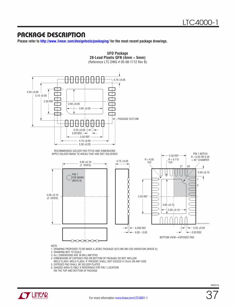
LTC4000-1
3740001fa
For more information www.linear.com/LTC4001-1
package DescripTionPlease refer to http://www.linear.com/designtools/packaging/ for the most recent package drawings.
4.00 ±0.10(2 SIDES)
2.50 REF
5.00 ±0.10(2 SIDES)
NOTE:1. DRAWING PROPOSED TO BE MADE A JEDEC PACKAGE OUTLINE MO-220 VARIATION (WXXX-X).2. DRAWING NOT TO SCALE3. ALL DIMENSIONS ARE IN MILLIMETERS4. DIMENSIONS OF EXPOSED PAD ON BOTTOM OF PACKAGE DO NOT INCLUDE MOLD FLASH. MOLD FLASH, IF PRESENT, SHALL NOT EXCEED 0.15mm ON ANY SIDE5. EXPOSED PAD SHALL BE SOLDER PLATED6. SHADED AREA IS ONLY A REFERENCE FOR PIN 1 LOCATION ON THE TOP AND BOTTOM OF PACKAGE
PIN 1TOP MARK(NOTE 6)
0.40 ±0.10
27 28
1
2
BOTTOM VIEW—EXPOSED PAD
3.50 REF
0.75 ±0.05 R = 0.115TYP
R = 0.05TYP
PIN 1 NOTCHR = 0.20 OR 0.35× 45° CHAMFER
0.25 ±0.05
0.50 BSC
0.200 REF
0.00 – 0.05
(UFD28) QFN 0506 REV B
RECOMMENDED SOLDER PAD PITCH AND DIMENSIONSAPPLY SOLDER MASK TO AREAS THAT ARE NOT SOLDERED
0.70 ±0.05
0.25 ±0.050.50 BSC
2.50 REF
3.50 REF4.10 ±0.055.50 ±0.05
2.65 ±0.05
3.10 ±0.054.50 ±0.05
PACKAGE OUTLINE
2.65 ±0.10
3.65 ±0.10
3.65 ±0.05
UFD Package28-Lead Plastic QFN (4mm × 5mm)
(Reference LTC DWG # 05-08-1712 Rev B)

LTC4000-1
3840001fa
For more information www.linear.com/LTC4001-1
package DescripTionPlease refer to http://www.linear.com/designtools/packaging/ for the most recent package drawings.
.386 – .393*(9.804 – 9.982)
GN28 REV B 0212
1 2 3 4 5 6 7 8 9 10 11 12
.229 – .244(5.817 – 6.198)
.150 – .157**(3.810 – 3.988)
202122232425262728 19 18 17
13 14
1615
.016 – .050(0.406 – 1.270)
.015 ±.004(0.38 ±0.10)
× 45°
0° – 8° TYP.0075 – .0098(0.19 – 0.25)
.0532 – .0688(1.35 – 1.75)
.008 – .012(0.203 – 0.305)
TYP
.004 – .0098(0.102 – 0.249)
.0250(0.635)
BSC
.033(0.838)
REF
.254 MIN
RECOMMENDED SOLDER PAD LAYOUT
.150 – .165
.0250 BSC.0165 ±.0015
.045 ±.005
* DIMENSION DOES NOT INCLUDE MOLD FLASH. MOLD FLASH SHALL NOT EXCEED 0.006" (0.152mm) PER SIDE** DIMENSION DOES NOT INCLUDE INTERLEAD FLASH. INTERLEAD FLASH SHALL NOT EXCEED 0.010" (0.254mm) PER SIDE
INCHES(MILLIMETERS)
NOTE:1. CONTROLLING DIMENSION: INCHES
2. DIMENSIONS ARE IN
3. DRAWING NOT TO SCALE4. PIN 1 CAN BE BEVEL EDGE OR A DIMPLE
GN Package28-Lead Plastic SSOP (Narrow .150 Inch)
(Reference LTC DWG # 05-08-1641 Rev B)
LTC4000-1
3940001fa
For more information www.linear.com/LTC4001-1
Information furnished by Linear Technology Corporation is believed to be accurate and reliable. However, no responsibility is assumed for its use. Linear Technology Corporation makes no representa-tion that the interconnection of its circuits as described herein will not infringe on existing patent rights.
revision hisToryREV DATE DESCRIPTION PAGE NUMBER
A 6/13 Clarified IGATE pin functionalityClarified Input Ideal Diode functionalityClarified Input Ideal Diode PMOS SelectionClarified Input UVLO and Voltage MonitoringRevised RCX C/X detection equationRevised Typical Application circuits (resistors)
1012 to 13
151618
11, 29, 34 to 36, 40
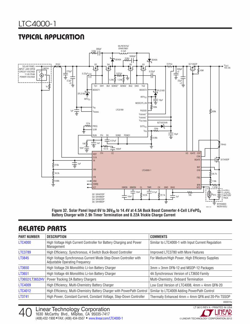
LTC4000-1
4040001fa
For more information www.linear.com/LTC4001-1 LINEAR TECHNOLOGY CORPORATION 2012
LT 0613 REV A • PRINTED IN USALinear Technology Corporation1630 McCarthy Blvd., Milpitas, CA 95035-7417(408) 432-1900 FAX: (408) 434-0507 www.linear.com/LTC4000-1
relaTeD parTs
Typical applicaTion
PART NUMBER DESCRIPTION COMMENTSLTC4000 High Voltage High Current Controller for Battery Charging and Power
ManagementSimilar to LTC4000-1 with Input Current Regulation
LTC3789 High Efficiency, Synchronous, 4 Switch Buck-Boost Controller Improved LTC3780 with More Features
LT3845 High Voltage Synchronous Current Mode Step-Down Controller with Adjustable Operating Frequency
For Medium/High Power, High Efficiency Supplies
LT3650 High Voltage 2A Monolithic Li-Ion Battery Charger 3mm × 3mm DFN-12 and MSOP-12 Packages
LT3651 High Voltage 4A Monolithic Li-Ion Battery Charger 4A Synchronous Version of LT3650 Family
LT3652/LT3652HV Power Tracking 2A Battery Chargers Multi-Chemistry, Onboard Termination
LTC4009 High Efficiency, Multi-Chemistry Battery Charger Low Cost Version of LTC4008, 4mm × 4mm QFN-20
LTC4012 High Efficiency, Multi-Chemistry Battery Charger with PowerPath Control Similar to LTC4009 Adding PowerPath Control
LT3741 High Power, Constant Current, Constant Voltage, Step-Down Controller Thermally Enhanced 4mm × 4mm QFN and 20-Pin TSSOP
Figure 32. Solar Panel Input 6V to 36VIN to 14.4V at 4.5A Buck Boost Converter 4-Cell LiFePO4 Battery Charger with 2.9h Timer Termination and 0.22A Trickle Charge Current
1.37M
14.7k
26.7k
10k RNTC
4-CELL LiFePO4BATTERY PACK
NTHS0603N02N1002J
Q2: SiR422DPQ3: SiR496DPQ4: SiR422DPQ5: SiR496DP
100nF
10mΩ
309k
VOUT15V, 5A
Si7135DP
118k
CSNCSP
BGATE
IGATE
BATOFB
FBG
BFBNTC
LTC4000-1
ITH CC IID
154k
BZT52C5V6
4mΩ 0.01Ω
LTC3789
EXTVCC
VFB
0.22µF
INTVCCINTVCC
BOOST2BOOST1
TG2SW2
MODE/PLLIN
PGOOD
ITHRUN SS SGND PGND1
FREQ
RSTCLNIN
ENCCHRGFLT
VM
1µF210k
16.2k
IFB
8.66k
VOUTSNS
IOSENSE–
IOSENSE+
SENSE–SENSE+
8.06k
100k
10µF
10µF
DFLS160
B240A
DFLS160
40001 F32
270µF
3.3µF×5
330µF×2
22µF×2
VIN
VINSNS1µF
ILIM
121k
Si7343DP
BG2BG1SW1TG1
Q5 Q3Q2 Q4
B240A
0.01µF
0.22µF
1.24k
0.01Ω
1.24k
5.6Ω390pF
IHLP6767GZER4R7M01
4.7µH
3.6Ω1800pF
R
LM234
V+
V–
SOLAR PANELINPUT <40V OPENCIRCUIT VOLTAGE
11.8V PEAKPOWER VOLTAGE
1k
CX
22.1k
CL TMRIIMON IBMON GND BIAS
18.2k1µF10nF
0.1µF10nF
10M
10nF
10k 1nF


![Sin título-1 · gplithwm 02430 gp cr2430 gp cr2430 gp urwum cr2430 super value —super super high voltage (4lr44] 476 a. high voltage high voltage voltage voltage](https://static.fdocuments.net/doc/165x107/5fc9a1e0f8d7c57bb3741c3c/sin-ttulo-1-gplithwm-02430-gp-cr2430-gp-cr2430-gp-urwum-cr2430-super-value-asuper.jpg)