LTC1871 - Wide Input Range, No RSENSE Current Mode …€¦ · LTC1871 3 1871fe ELECTRICAL...
36
LTC1871 1 1871fe TYPICAL APPLICATION FEATURES APPLICATIONS DESCRIPTION Wide Input Range, No R SENSE ™ Current Mode Boost, Flyback and SEPIC Controller The LTC ® 1871 is a wide input range, current mode, boost, flyback or SEPIC controller that drives an N-channel power MOSFET and requires very few external components. In- tended for low to medium power applications, it eliminates the need for a current sense resistor by utilizing the power MOSFET’s on-resistance, thereby maximizing efficiency. The IC’s operating frequency can be set with an external resistor over a 50kHz to 1MHz range, and can be syn- chronized to an external clock using the MODE/SYNC pin. Burst Mode operation at light loads, a low minimum operating supply voltage of 2.5V and a low shutdown quiescent current of 10μA make the LTC1871 ideally suited for battery-operated systems. For applications requiring constant frequency opera- tion, Burst Mode operation can be defeated using the MODE/SYNC pin. Higher output voltage boost, SEPIC and flyback applications are possible with the LTC1871 by connecting the SENSE pin to a resistor in the source of the power MOSFET. The LTC1871 is available in the 10-lead MSOP package. Efficiency of Figure 1 n High Efficiency (No Sense Resistor Required) n Wide Input Voltage Range: 2.5V to 36V n Current Mode Control Provides Excellent Transient Response n High Maximum Duty Cycle (92% Typ) n ±2% RUN Pin Threshold with 100mV Hysteresis n ±1% Internal Voltage Reference n Micropower Shutdown: I Q = 10μA n Programmable Operating Frequency (50kHz to 1MHz) with One External Resistor n Synchronizable to an External Clock Up to 1.3 × f OSC n User-Controlled Pulse Skip or Burst Mode ® Operation n Internal 5.2V Low Dropout Voltage Regulator n Output Overvoltage Protection n Capable of Operating with a Sense Resistor for High Output Voltage Applications n Small 10-Lead MSOP Package n Telecom Power Supplies n Portable Electronic Equipment L, LT, LTC, LTM and Burst Mode are registered trademarks of Linear Technology Corporation. No R SENSE is a trademark of Linear Technology Corporation. All other trademarks are the property of their respective owners. Figure 1. High Efficiency 3.3V Input, 5V Output Boost Converter (Bootstrapped) + RUN I TH FB FREQ MODE/SYNC SENSE V IN INTV CC GATE GND LTC1871 R T 80.6k 1% R2 37.4k 1% R1 12.1k 1% C VCC 4.7μF X5R C IN 22μF 6.3V ×2 M1 D1 L1 1μH R C 22k C C1 6.8nF C C2 47pF C OUT1 150μF 6.3V ×4 V IN 3.3V V OUT 5V 7A (10A PEAK) GND 1871 F01a + C OUT2 22μF 6.3V X5R ×2 C IN : TAIYO YUDEN JMK325BJ226MM C OUT1 : PANASONIC EEFUEOJ151R C OUT2 : TAIYO YUDEN JMK325BJ226MM D1: MBRB2515L L1: SUMIDA CEP125-H 1R0MH M1: FAIRCHILD FDS7760A OUTPUT CURRENT (A) 30 EFFICIENCY (%) 90 100 80 50 70 60 40 0.001 0.1 1 10 1871 F01b 0.01 Burst Mode OPERATION PULSE-SKIP MODE
Transcript of LTC1871 - Wide Input Range, No RSENSE Current Mode …€¦ · LTC1871 3 1871fe ELECTRICAL...

LTC1871
11871fe
TYPICAL APPLICATION
FEATURES
APPLICATIONS
DESCRIPTION
Wide Input Range, No RSENSE™ Current Mode Boost,
Flyback and SEPIC Controller
The LTC®1871 is a wide input range, current mode, boost, fl yback or SEPIC controller that drives an N-channel power MOSFET and requires very few external components. In-tended for low to medium power applications, it eliminates the need for a current sense resistor by utilizing the power MOSFET’s on-resistance, thereby maximizing effi ciency.
The IC’s operating frequency can be set with an external resistor over a 50kHz to 1MHz range, and can be syn-chronized to an external clock using the MODE/SYNC pin. Burst Mode operation at light loads, a low minimum operating supply voltage of 2.5V and a low shutdown quiescent current of 10μA make the LTC1871 ideally suited for battery-operated systems.
For applications requiring constant frequency opera-tion, Burst Mode operation can be defeated using the MODE/SYNC pin. Higher output voltage boost, SEPIC and fl yback applications are possible with the LTC1871 by connecting the SENSE pin to a resistor in the source of the power MOSFET.
The LTC1871 is available in the 10-lead MSOP package.
Effi ciency of Figure 1
n High Effi ciency (No Sense Resistor Required)n Wide Input Voltage Range: 2.5V to 36Vn Current Mode Control Provides Excellent Transient Responsen High Maximum Duty Cycle (92% Typ)n ±2% RUN Pin Threshold with 100mV Hysteresisn ±1% Internal Voltage Referencen Micropower Shutdown: IQ = 10μAn Programmable Operating Frequency (50kHz to 1MHz) with One External Resistorn Synchronizable to an External Clock Up to 1.3 × fOSCn User-Controlled Pulse Skip or Burst Mode® Operationn Internal 5.2V Low Dropout Voltage Regulatorn Output Overvoltage Protectionn Capable of Operating with a Sense Resistor for High Output Voltage Applicationsn Small 10-Lead MSOP Package
n Telecom Power Suppliesn Portable Electronic Equipment
L, LT, LTC, LTM and Burst Mode are registered trademarks of Linear Technology Corporation. No RSENSE is a trademark of Linear Technology Corporation. All other trademarks are the property of their respective owners.
Figure 1. High Effi ciency 3.3V Input, 5V Output Boost Converter (Bootstrapped)
+
RUN
ITH
FB
FREQ
MODE/SYNC
SENSE
VIN
INTVCC
GATE
GND
LTC1871
RT80.6k1%
R237.4k
1%
R112.1k1% CVCC
4.7μFX5R
CIN22μF6.3V×2
M1
D1
L11μH
RC22k
CC16.8nF
CC247pF
COUT1150μF6.3V×4
VIN3.3V
VOUT5V7A(10A PEAK)
GND1871 F01a
+
COUT222μF6.3VX5R×2
CIN: TAIYO YUDEN JMK325BJ226MMCOUT1: PANASONIC EEFUEOJ151RCOUT2: TAIYO YUDEN JMK325BJ226MM
D1: MBRB2515LL1: SUMIDA CEP125-H 1R0MHM1: FAIRCHILD FDS7760A
OUTPUT CURRENT (A)
30
EFF
ICIE
NC
Y (
%)
90
100
80
50
70
60
40
0.001 0.1 1 10
1871 F01b
0.01
Burst ModeOPERATION
PULSE-SKIPMODE

LTC1871
21871fe
PIN CONFIGURATION ABSOLUTE MAXIMUM RATINGS
VIN Voltage ............................................... –0.3V to 36VINTVCC Voltage ............................................ –0.3V to 7VINTVCC Output Current .......................................... 50mAGATE Voltage ............................ –0.3V to VINTVCC + 0.3VITH, FB Voltages ....................................... –0.3V to 2.7VRUN, MODE/SYNC Voltages ....................... –0.3V to 7VFREQ Voltage ............................................ –0.3V to 1.5VSENSE Pin Voltage .................................... –0.3V to 36VOperating Temperature Range (Note 2) LTC1871E ............................................. –40°C to 85°C LTC1871I............................................ –40°C to 125°C LTC1871H .......................................... –40°C to 150°CJunction Temperature (Note 3) LTC1871E/LTC1871I ......................................... 125°C LTC1871H ......................................................... 150°CStorage Temperature Range ................... –65°C to 150°CLead Temperature (Soldering, 10 sec) .................. 300°C
(Note 1)
12345
RUNITHFB
FREQMODE/SYNC
109876
SENSEVININTVCCGATEGND
TOP VIEW
MS PACKAGE10-LEAD PLASTIC MSOP
TJMAX = 125°C, θJA = 120°C/W
ORDER INFORMATIONLEAD FREE FINISH TAPE AND REEL PART MARKING PACKAGE DESCRIPTION TEMPERATURE RANGE
LTC1871EMS#PBF LTC1871EMS#TRPBF LTSX 10-Lead Plastic MSOP –40°C to 85°C
LTC1871IMS#PBF LTC1871IMS#TRPBF LTBFC 10-Lead Plastic MSOP –40°C to 125°C
LTC1871HMS#PBF LTC1871HMS#TRPBF LTCXS 10-Lead Plastic MSOP –40°C to 150°C
LEAD BASED FINISH TAPE AND REEL PART MARKING PACKAGE DESCRIPTION TEMPERATURE RANGE
LTC1871EMS LTC1871EMS#TR LTSX 10-Lead Plastic MSOP –40°C to 85°C
LTC1871IMS LTC1871IMS#TR LTBFC 10-Lead Plastic MSOP –40°C to 125°C
LTC1871HMS LTC1871HMS#TR LTCXS 10-Lead Plastic MSOP –40°C to 150°C
Consult LTC Marketing for parts specifi ed with wider operating temperature ranges.
For more information on lead free part marking, go to: http://www.linear.com/leadfree/ For more information on tape and reel specifi cations, go to: http://www.linear.com/tapeandreel/

LTC1871
31871fe
ELECTRICAL CHARACTERISTICS The l denotes the specifi cations which apply over the full operating temperature range, otherwise specifi cations are at TA = 25°C. VIN = VINTVCC = 5V, VRUN = 1.5V, RFREQ = 80k, VMODE/SYNC = 0V, unless otherwise specifi ed.
SYMBOL PARAMETER CONDITIONS MIN TYP MAX UNITS
Main Control Loop
VIN(MIN) Minimum Input Voltage 2.5 V
I-Grade or H-Grade (Note 2) ● 2.5 V
IQ Input Voltage Supply Current (Note 4)
Continuous Mode VMODE/SYNC = 5V, VFB = 1.4V, VITH = 0.75V 550 1000 μA
VMODE/SYNC = 5V, VFB = 1.4V, VITH = 0.75V,I-Grade or H-Grade (Note 2)
● 550 1000 μA
Burst Mode Operation, No Load VMODE/SYNC = 0V, VITH = 0.2V (Note 5) 250 500 μA
VMODE/SYNC = 0V, VITH = 0.2V (Note 5),I-Grade or H-Grade (Note 2)
● 250 500 μA
Shutdown Mode VRUN = 0V 10 20 μA
VRUN = 0V, I-Grade or H-Grade (Note 2) ● 10 20 μA
VRUN+ Rising RUN Input Threshold Voltage 1.348 V
VRUN– Falling RUN Input Threshold Voltage
●
1.2231.198
1.248 1.2731.298
VV
H-Grade (Note 2) ● 1.179 1.315 V
VRUN(HYST) RUN Pin Input Threshold Hysteresis 50 100 150 mV
I-Grade (Note 2) ● 35 100 175 mV
H-Grade (Note 2) ● 35 300 mV
IRUN RUN Input Current 1 60 nA
VFB Feedback Voltage VITH = 0.2V (Note 5)●
1.2181.212
1.230 1.2421.248
VV
VITH = 0.2V (Note 5), I-Grade or H-Grade (Note 2) ● 1.205 1.255 V
IFB FB Pin Input Current VITH = 0.2V (Note 5) 18 60 nA
ΔVFB
ΔVIN
Line Regulation 2.5V ≤ VIN ≤ 30V 0.002 0.02 %/V
2.5V ≤ VIN ≤ 30V, I-Grade or H-Grade (Note 2) ● 0.002 0.02 %/V
ΔVFB
ΔVITH
Load Regulation VMODE/SYNC = 0V, VITH = 0.5V to 0.9V (Note 5) ● –1 –0.1 %
VMODE/SYNC = 0V, VITH = 0.5V to 0.9V (Note 5)I-Grade or H-Grade (Note 2)
● –1 –0.1 %
ΔVFB(OV) ΔFB Pin, Overvoltage Lockout VFB(OV) – VFB(NOM) in Percent 2.5 6 10 %
gm Error Amplifi er Transconductance ITH Pin Load = ±5μA (Note 5) 650 μmho
VITH(BURST) Burst Mode Operation ITH Pin Voltage Falling ITH Voltage (Note 5) 0.3 V
VSENSE(MAX) Maximum Current Sense Input Threshold Duty Cycle < 20% 120 150 180 mV
Duty Cycle < 20%, I-Grade or H-Grade (Note 2) ● 100 200 mV
ISENSE(ON) SENSE Pin Current (GATE High) VSENSE = 0V 35 50 μA
ISENSE(OFF) SENSE Pin Current (GATE Low) VSENSE = 30V 0.1 5 μA
Oscillator
fOSC Oscillator Frequency RFREQ = 80k 250 300 350 kHz
RFREQ = 80k, I-Grade (Note 2) ● 250 300 350 kHz
RFREQ = 80k, H-Grade (Note 2) ● 240 300 360 kHz
Oscillator Frequency Range 50 1000 kHz
I-Grade or H-Grade (Note 2) ● 50 1000 kHz

LTC1871
41871fe
ELECTRICAL CHARACTERISTICS The l denotes the specifi cations which apply over the full operating temperature range, otherwise specifi cations are at TA = 25°C. VIN = VINTVCC = 5V, VRUN = 1.5V, RFREQ = 80k, VMODE/SYNC = 0V, unless otherwise specifi ed.
SYMBOL PARAMETER CONDITIONS MIN TYP MAX UNITS
DMAX Maximum Duty Cycle 87 92 97 %
I-Grade or H-Grade (Note 2) ● 87 92 97 %
fSYNC/fOSC Recommended Maximum Synchronized Frequency Ratio
fOSC = 300kHz (Note 6) 1.25 1.30
fOSC = 300kHz (Note 6), I-Grade or H-Grade (Note 2) ● 1.25 1.30
tSYNC(MIN) MODE/SYNC Minimum Input Pulse Width VSYNC = 0V to 5V 25 ns
tSYNC(MAX) MODE/SYNC Maximum Input Pulse Width VSYNC = 0V to 5V 0.8/fOSC ns
VIL(MODE) Low Level MODE/SYNC Input Voltage 0.3 V
I-Grade or H-Grade (Note 2) ● 0.3 V
VIH(MODE) High Level MODE/SYNC Input Voltage 1.2 V
I-Grade or H-Grade (Note 2) ● 1.2 V
RMODE/SYNC MODE/SYNC Input Pull-Down Resistance 50 kΩ
VFREQ Nominal FREQ Pin Voltage 0.62 V
Low Dropout Regulator
VINTVCC INTVCC Regulator Output Voltage VIN = 7.5V 5.0 5.2 5.4 V
VIN = 7.5V, I-Grade (Note 2) ● 5.0 5.2 5.4 V
VIN = 7.5V, H-Grade (Note 2) ● 4.95 5.2 5.45 V
ΔVINTVCC
ΔVIN1
INTVCC Regulator Line Regulation 7.5V ≤ VIN ≤ 15V 8 25 mV
ΔVINTVCC
ΔVIN2
INTVCC Regulator Line Regulation 15V ≤ VIN ≤ 30V 70 200 mV
VLDO(LOAD) INTVCC Load Regulation 0 ≤ IINTVCC ≤ 20mA, VIN = 7.5V –2 –0.2 %
VDROPOUT INTVCC Regulator Dropout Voltage VIN = 5V, INTVCC Load = 20mA 280 mV
IINTVCC Bootstrap Mode INTVCC SupplyCurrent in Shutdown
RUN = 0V, SENSE = 5V 10 20 μA
I-Grade (Note 2) ● 30 μA
H-Grade (Note 2) ● 50 μA
GATE Driver
tr GATE Driver Output Rise Time CL = 3300pF (Note 7) 17 100 ns
tf GATE Driver Output Fall Time CL = 3300pF (Note 7) 8 100 ns
Note 1: Stresses beyond those listed under Absolute Maximum Ratings
may cause permanent damage to the device. Exposure to any Absolute
Maximum Rating condition for extended periods may affect device
reliability and lifetime.
Note 2: The LTC1871E is guaranteed to meet performance specifi cations
from 0°C to 85°C operating temperature. Specifi cations over the –40°C to
85°C operating temperature range are assured by design, characterization
and correlation with statistical process controls. The LTC1871I is
guaranteed over the full –40°C to 125°C operating temperature range
and the LTC1871H is guaranteed over the full –40°C to 150°C operating
temperature range.
Note 3: TJ is calculated from the ambient temperature TA and power
dissipation PD according to the following formula:
TJ = TA + (PD • 110°C/W)
Note 4: The dynamic input supply current is higher due to power MOSFET
gate charging (QG • fOSC). See Applications Information.
Note 5: The LTC1871 is tested in a feedback loop which servos VFB to
the reference voltage with the ITH pin forced to the midpoint of its voltage
range (0.3V ≤ VITH ≤ 1.2V, midpoint = 0.75V).
Note 6: In a synchronized application, the internal slope compensation
gain is increased by 25%. Synchronizing to a signifi cantly higher ratio will
reduce the effective amount of slope compensation, which could result in
subharmonic oscillation for duty cycles greater than 50%.
Note 7: Rise and fall times are measured at 10% and 90% levels.

LTC1871
51871fe
TYPICAL PERFORMANCE CHARACTERISTICS
FB Voltage vs Temp FB Voltage Line Regulation FB Pin Current vs Temperature
Shutdown Mode IQ vs VIN Shutdown Mode IQ vs Temperature Burst Mode IQ vs VIN
Burst Mode IQ vs Temperature Dynamic IQ vs FrequencyGate Drive Rise and Fall Time vs CL
TEMPERATURE (°C)
–50
FB V
OLTA
GE (
V)
1.23
1.24
150
1871 G01
1.22
1.210 50 100–25 25 75 125
1.25
VIN (V)
01.229
FB V
OLTA
GE (
V)
1.230
1.231
5 10 15 20
1871 G02
25 30 35
TEMPERATURE (°C)
–500
FB P
IN C
UR
REN
T (
nA
)
10
20
30
40
60
–25 250 50 10075
1871 G03
125 150
50
VIN (V)
00
SH
UTD
OW
N M
OD
E I
Q (
μA
)
10
20
10 20 30 40
1871 G04
30
TEMPERATURE (°C)
–500
SH
UTD
OW
N M
OD
E I
Q (
μA
)
5
10
15
20
–25 0 25 50
1871 G05
75 100 125 150
VIN = 5V
VIN (V)
00
Burs
t M
ode
I Q (
μA
)
100
200
300
400
600
10 20
1871 G06
30 40
500
TEMPERATURE (°C)
–500
Burs
t M
ode
I Q (
μA
)
200
500
0 50 75
1871 G07
100
400
300
–25 25 100 125 150
FREQUENCY (kHz)
00
I Q (
mA
)
2
6
8
10
800
18
1871 G08
4
400 1200600200 1000
12
14
16
CL = 3300pFIQ(TOT) = 550μA + Qg • f
CL (pF)
00
TIM
E (
ns)
10
20
30
40
60
2000 4000 6000 8000
1871 G09
10000 12000
50
RISE TIME
FALL TIME

LTC1871
61871fe
TYPICAL PERFORMANCE CHARACTERISTICS
RUN Thresholds vs VIN RUN Thresholds vs Temperature RT vs Frequency
Frequency vs TemperatureMaximum Sense Threshold vs Temperature
SENSE Pin Current vs Temperature
INTVCC Load Regulation INTVCC Line RegulationINTVCC Dropout Voltagevs Current, Temperature
VIN (V)
01.2
RU
N T
HR
ES
HO
LD
S (
V)
1.3
1.4
10 20 30 40
1871 G10
1.5
TEMPERATURE (°C)
–50
RU
N T
HR
ES
HO
LD
S (
V)
1.30
1.35
150
1871 G11
1.25
1.200 50 100–25 25 75 125
1.40
FREQUENCY (kHz)
100
RT (
kΩ)
300
1000
1871 G12
10
100
200 10009008007006005004000
TEMPERATURE (°C)
–50275
GA
TE F
REQ
UEN
CY
(kH
z)
280
290
295
300
325
310
0 50 75
1871 G13
285
315
320
305
–25 25 100 125 150
TEMPERATURE (°C)
–50140
MA
X S
EN
SE T
HR
ES
HO
LD
(m
V)
145
150
155
160
–25 0 25 50
1871 G14
75 100 125 150
TEMPERATURE (°C)
–5025
SEN
SE P
IN C
UR
REN
T (
μA
)
30
35
0 50 75
1871 G15
–25 25 100 125 150
GATE HIGHVSENSE = 0V
INTVCC LOAD (mA)
0
INTV
CC V
OLTA
GE (
V)
5.2
30 50 80
1871 G16
5.1
5.010 20 40 60 70
VIN = 7.5V
VIN (V)
05.1
INTV
CC V
OLTA
GE (
V)
5.2
5.3
10 20 30 40
1871 G17
5.4
5 15 25 35
INTVCC LOAD (mA)
00
DR
OP
OU
T V
OLTA
GE (
mV
)
50
150
200
250
500
350
5 10
1871 G18
100
400
450
300
15 20
150°C
75°C
125°C
25°C
–50°C
0°C

LTC1871
71871fe
PIN FUNCTIONSRUN (Pin 1): The RUN pin provides the user with an accurate means for sensing the input voltage and pro-gramming the start-up threshold for the converter. The falling RUN pin threshold is nominally 1.248V and the comparator has 100mV of hysteresis for noise immunity. When the RUN pin is below this input threshold, the IC is shut down and the VIN supply current is kept to a low value (typ 10μA). The Absolute Maximum Rating for the voltage on this pin is 7V.
ITH (Pin 2): Error Amplifi er Compensation Pin. The current comparator input threshold increases with this control voltage. Nominal voltage range for this pin is 0V to 1.40V.
FB (Pin 3): Receives the feedback voltage from the external resistor divider across the output. Nominal voltage for this pin in regulation is 1.230V.
FREQ (Pin 4): A resistor from the FREQ pin to ground programs the operating frequency of the chip. The nominal voltage at the FREQ pin is 0.6V.
MODE/SYNC (Pin 5): This input controls the operating mode of the converter and allows for synchronizing the
operating frequency to an external clock. If the MODE/SYNC pin is connected to ground, Burst Mode operation is enabled. If the MODE/SYNC pin is connected to INTVCC, or if an external logic-level synchronization signal is ap-plied to this input, Burst Mode operation is disabled and the IC operates in a continuous mode.
GND (Pin 6): Ground Pin.
GATE (Pin 7): Gate Driver Output.
INTVCC (Pin 8): The Internal 5.20V Regulator Output. The gate driver and control circuits are powered from this voltage. Decouple this pin locally to the IC ground with a minimum of 4.7μF low ESR tantalum or ceramic capacitor.
VIN (Pin 9): Main Supply Pin. Must be closely decoupled to ground.
SENSE (Pin 10): The Current Sense Input for the Control Loop. Connect this pin to the drain of the power MOSFET for VDS sensing and highest effi ciency. Alternatively, the SENSE pin may be connected to a resistor in the source of the power MOSFET. Internal leading edge blanking is provided for both sensing methods.

LTC1871
81871fe
BLOCK DIAGRAM
–
+
–
+
+1.230V
85mVOV
50k
EA
UV
TOSTART-UPCONTROL
BURSTCOMPARATOR
S
RQ
LOGICPWM LATCH
CURRENTCOMPARATOR
0.30V
1.230V
5.2V
–
+2.00V
1.230VSLOPE
1.230V
ILOOP
FB
ITH
–
+
gm
3
MODE/SYNC
5
FREQ
4
2
INTVCC
8 LDO
V-TO-I
OSCV-TO-I
SLOPECOMPENSATION
BIAS ANDSTART-UPCONTROL
VIN
BIAS VREF
IOSC
RLOOP
–
+
–
+
C1
SENSE
10
GND
1871 BD
6
GATE
INTVCC
GND
7
VIN
1.248V
9
RUN
C2
1
0.6V
Main Control Loop
The LTC1871 is a constant frequency, current mode con-troller for DC/DC boost, SEPIC and fl yback converter ap-plications. The LTC1871 is distinguished from conventional current mode controllers because the current control loop can be closed by sensing the voltage drop across the power MOSFET switch instead of across a discrete sense resistor, as shown in Figure 2. This sensing technique improves effi ciency, increases power density, and reduces the cost of the overall solution.
For circuit operation, please refer to the Block Diagram of the IC and Figure 1. In normal operation, the power MOSFET
is turned on when the oscillator sets the PWM latch and is turned off when the current comparator C1 resets the latch. The divided-down output voltage is compared to an internal 1.230V reference by the error amplifi er EA, which outputs an error signal at the ITH pin. The voltage on the ITH pin sets the current comparator C1 input threshold. When the load current increases, a fall in the FB voltage relative to the reference voltage causes the ITH pin to rise, which causes the current comparator C1 to trip at a higher peak inductor current value. The average inductor current will therefore rise until it equals the load current, thereby maintaining output regulation.
OPERATION
LTC1871
91871fe
OPERATION
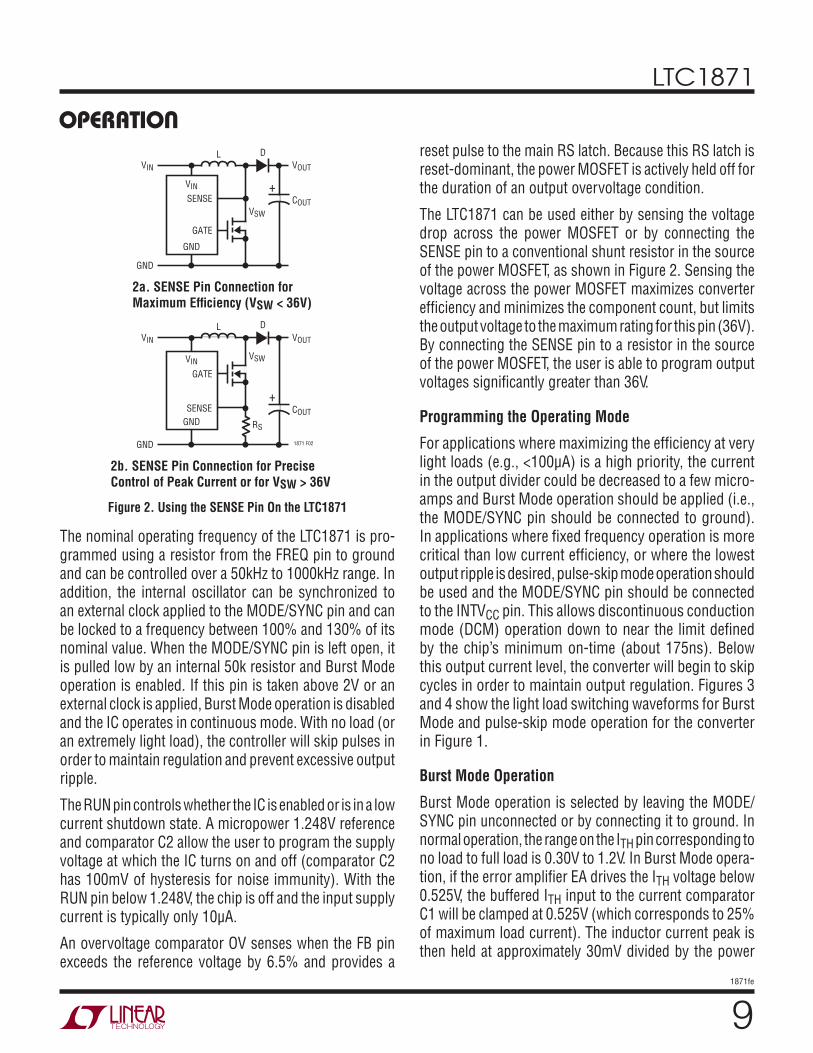
Figure 2. Using the SENSE Pin On the LTC1871
reset pulse to the main RS latch. Because this RS latch is reset-dominant, the power MOSFET is actively held off for the duration of an output overvoltage condition.
The LTC1871 can be used either by sensing the voltage drop across the power MOSFET or by connecting the SENSE pin to a conventional shunt resistor in the source of the power MOSFET, as shown in Figure 2. Sensing the voltage across the power MOSFET maximizes converter effi ciency and minimizes the component count, but limits the output voltage to the maximum rating for this pin (36V). By connecting the SENSE pin to a resistor in the source of the power MOSFET, the user is able to program output voltages signifi cantly greater than 36V.
Programming the Operating Mode
For applications where maximizing the effi ciency at very light loads (e.g., <100μA) is a high priority, the current in the output divider could be decreased to a few micro-amps and Burst Mode operation should be applied (i.e., the MODE/SYNC pin should be connected to ground). In applications where fi xed frequency operation is more critical than low current effi ciency, or where the lowest output ripple is desired, pulse-skip mode operation should be used and the MODE/SYNC pin should be connected to the INTVCC pin. This allows discontinuous conduction mode (DCM) operation down to near the limit defi ned by the chip’s minimum on-time (about 175ns). Below this output current level, the converter will begin to skip cycles in order to maintain output regulation. Figures 3 and 4 show the light load switching waveforms for Burst Mode and pulse-skip mode operation for the converter in Figure 1.
Burst Mode Operation
Burst Mode operation is selected by leaving the MODE/SYNC pin unconnected or by connecting it to ground. In normal operation, the range on the ITH pin corresponding to no load to full load is 0.30V to 1.2V. In Burst Mode opera-tion, if the error amplifi er EA drives the ITH voltage below 0.525V, the buffered ITH input to the current comparator C1 will be clamped at 0.525V (which corresponds to 25% of maximum load current). The inductor current peak is then held at approximately 30mV divided by the power
COUTVSW
VSW
2a. SENSE Pin Connection for
Maximum Efficiency (VSW < 36V)
VOUTVIN
GND
L D
+
COUT
RS
1871 F02
2b. SENSE Pin Connection for Precise
Control of Peak Current or for VSW > 36V
VOUTVIN
GND
L D
+
GATE
GND
VIN
SENSE
GATE
GND
VIN
SENSE
The nominal operating frequency of the LTC1871 is pro-grammed using a resistor from the FREQ pin to ground and can be controlled over a 50kHz to 1000kHz range. In addition, the internal oscillator can be synchronized to an external clock applied to the MODE/SYNC pin and can be locked to a frequency between 100% and 130% of its nominal value. When the MODE/SYNC pin is left open, it is pulled low by an internal 50k resistor and Burst Mode operation is enabled. If this pin is taken above 2V or an external clock is applied, Burst Mode operation is disabled and the IC operates in continuous mode. With no load (or an extremely light load), the controller will skip pulses in order to maintain regulation and prevent excessive output ripple.
The RUN pin controls whether the IC is enabled or is in a low current shutdown state. A micropower 1.248V reference and comparator C2 allow the user to program the supply voltage at which the IC turns on and off (comparator C2 has 100mV of hysteresis for noise immunity). With the RUN pin below 1.248V, the chip is off and the input supply current is typically only 10μA.
An overvoltage comparator OV senses when the FB pin exceeds the reference voltage by 6.5% and provides a

LTC1871
101871fe
MOSFET RDS(ON). If the ITH pin drops below 0.30V, the Burst Mode comparator B1 will turn off the power MOSFET and scale back the quiescent current of the IC to 250μA (sleep mode). In this condition, the load current will be supplied by the output capacitor until the ITH voltage rises above the 50mV hysteresis of the burst comparator. At light loads, short bursts of switching (where the average inductor current is 20% of its maximum value) followed by long periods of sleep will be observed, thereby greatly improving converter effi ciency. Oscilloscope waveforms illustrating Burst Mode operation are shown in Figure 3.
Pulse-Skip Mode Operation
With the MODE/SYNC pin tied to a DC voltage above 2V, Burst Mode operation is disabled. The internal, 0.525V buffered ITH burst clamp is removed, allowing the ITH pin to directly control the current comparator from no load to full load. With no load, the ITH pin is driven below 0.30V, the power MOSFET is turned off and sleep mode is invoked. Oscilloscope waveforms illustrating this mode of operation are shown in Figure 4.
When an external clock signal drives the MODE/SYNC pin at a rate faster than the chip’s internal oscillator, the oscillator will synchronize to it. In this synchronized mode, Burst Mode operation is disabled. The constant frequency associated with synchronized operation provides a more controlled noise spectrum from the converter, at the ex-pense of overall system effi ciency of light loads.
When the oscillator’s internal logic circuitry detects a synchronizing signal on the MODE/SYNC pin, the in-ternal oscillator ramp is terminated early and the slope compensation is increased by approximately 30%. As a result, in applications requiring synchronization, it is recommended that the nominal operating frequency of the IC be programmed to be about 75% of the external clock frequency. Attempting to synchronize to too high an external frequency (above 1.3fO) can result in inadequate slope compensation and possible subharmonic oscillation (or jitter).
The external clock signal must exceed 2V for at least 25ns, and should have a maximum duty cycle of 80%, as shown in Figure 5. The MOSFET turn on will synchronize to the rising edge of the external clock signal.
Figure 3. LTC1871 Burst Mode Operation (MODE/SYNC = 0V) at Low Output Current
Figure 4. LTC1871 Low Output Current Operation with Burst Mode Operation Disabled (MODE/SYNC = INTVCC)
VOUT50mV/DIV
IL5A/DIV
10μs/DIV1871 F03
VIN = 3.3VVOUT = 5VIOUT = 500mA
MODE/SYNC = 0V(Burst Mode OPERATION)
VOUT50mV/DIV
IL5A/DIV
2μs/DIV1871 F04
VIN = 3.3VVOUT = 5VIOUT = 500mA
MODE/SYNC = INTVCC(PULSE-SKIP MODE)
OPERATION
Figure 5. MODE/SYNC Clock Input and Switching Waveforms for Synchronized Operation
1871 F05
2V TO 7VMODE/SYNC
GATE
IL
tMIN = 25ns
0.8T
D = 40%
T T = 1/fO

LTC1871
111871fe
APPLICATIONS INFORMATIONProgramming the Operating Frequency
The choice of operating frequency and inductor value is a tradeoff between effi ciency and component size. Low frequency operation improves effi ciency by reducing MOSFET and diode switching losses. However, lower frequency operation requires more inductance for a given amount of load current.
The LTC1871 uses a constant frequency architecture that can be programmed over a 50kHz to 1000kHz range with a single external resistor from the FREQ pin to ground, as shown in Figure 1. The nominal voltage on the FREQ pin is 0.6V, and the current that fl ows into the FREQ pin is used to charge and discharge an internal oscillator capacitor. A graph for selecting the value of RT for a given operating frequency is shown in Figure 6.
INTVCC Regulator Bypassing and Operation
An internal, P-channel low dropout voltage regulator pro-duces the 5.2V supply which powers the gate driver and logic circuitry within the LTC1871, as shown in Figure 7. The INTVCC regulator can supply up to 50mA and must be bypassed to ground immediately adjacent to the IC pins with a minimum of 4.7μF tantalum or ceramic capacitor. Good bypassing is necessary to supply the high transient currents required by the MOSFET gate driver.
For input voltages that don’t exceed 7V (the absolute maximum rating for this pin), the internal low dropout regulator in the LTC1871 is redundant and the INTVCC pin can be shorted directly to the VIN pin. With the INTVCC pin shorted to VIN, however, the divider that programs the regulated INTVCC voltage will draw 10μA of current from the input supply, even in shutdown mode. For applications that require the lowest shutdown mode input supply cur-rent, do not connect the INTVCC pin to VIN. Regardless of whether the INTVCC pin is shorted to VIN or not, it is always necessary to have the driver circuitry bypassed with a 4.7μF tantalum or low ESR ceramic capacitor to ground immediately adjacent to the INTVCC and GND pins.
In an actual application, most of the IC supply current is used to drive the gate capacitance of the power MOSFET. As a result, high input voltage applications in which a large power MOSFET is being driven at high frequencies can cause the LTC1871 to exceed its maximum junction
Figure 6. Timing Resistor (RT) Value
FREQUENCY (kHz)
100
RT (
kΩ)
300
1000
1871 F06
10
100
200 10009008007006005004000
Figure 7. Bypassing the LDO Regulator and Gate Driver Supply
+
–
+
1.230V
R2 R1
P-CH
5.2V
DRIVERGATE
CVCC4.7μF
CIN
INPUTSUPPLY2.5V TO 30V
GND
PLACE AS CLOSE ASPOSSIBLE TO DEVICE PINS
M1
1871 F07
INTVCC
VIN
GND
LOGIC

LTC1871
121871fe
APPLICATIONS INFORMATIONtemperature rating. The junction temperature can be estimated using the following equations:
IQ(TOT) ≈ IQ + f • QG
PIC = VIN • (IQ + f • QG)
TJ = TA + PIC • RTH(JA)
The total quiescent current IQ(TOT) consists of the static supply current (IQ) and the current required to charge and discharge the gate of the power MOSFET. The 10-pin MSOP package has a thermal resistance of RTH(JA) = 120°C/W.
As an example, consider a power supply with VIN = 5V and VO = 12V at IO = 1A. The switching frequency is 500kHz, and the maximum ambient temperature is 70°C. The power MOSFET chosen is the IRF7805, which has a maximum RDS(ON) of 11mΩ (at room temperature) and a maximum total gate charge of 37nC (the temperature coeffi cient of the gate charge is low).
IQ(TOT) = 600μA + 37nC • 500kHz = 19.1mA
PIC = 5V • 19.1mA = 95mW
TJ = 70°C + 120°C/W • 95mW = 81.4°C
This demonstrates how signifi cant the gate charge current can be when compared to the static quiescent current in the IC.
To prevent the maximum junction temperature from being exceeded, the input supply current must be checked when operating in a continuous mode at high VIN. A tradeoff between the operating frequency and the size of the power MOSFET may need to be made in order to maintain a reliable IC junction temperature. Prior to lowering the operating frequency, however, be sure to check with power MOSFET manufacturers for their latest-and-greatest low QG, low RDS(ON) devices. Power MOSFET manufacturing tech-nologies are continually improving, with newer and better performance devices being introduced almost yearly.
Output Voltage Programming
The output voltage is set by a resistor divider according to the following formula:
VO =1.230V • 1+
R2
R1
The external resistor divider is connected to the output as shown in Figure 1, allowing remote voltage sensing. The resistors R1 and R2 are typically chosen so that the error caused by the current fl owing into the FB pin dur-ing normal operation is less than 1% (this translates to a maximum value of R1 of about 250k).
Programming Turn-On and Turn-Off Thresholds with the RUN Pin
The LTC1871 contains an independent, micropower voltage reference and comparator detection circuit that remains active even when the device is shut down, as shown in Figure 8. This allows users to accurately program an input voltage at which the converter will turn on and off. The falling threshold voltage on the RUN pin is equal to the internal reference voltage of 1.248V. The comparator has 100mV of hysteresis to increase noise immunity.
The turn-on and turn-off input voltage thresholds are programmed using a resistor divider according to the following formulas:
VIN(OFF) =1.248V • 1+R2
R1
VIN(ON) =1.348V • 1+R2
R1
The resistor R1 is typically chosen to be less than 1M.
For applications where the RUN pin is only to be used as a logic input, the user should be aware of the 7V Absolute Maximum Rating for this pin! The RUN pin can be con-nected to the input voltage through an external 1M resistor, as shown in Figure 8c, for “always on” operation.
Application Circuits
A basic LTC1871 application circuit is shown in Figure 1. External component selection is driven by the character-istics of the load and the input supply. The fi rst topology to be analyzed will be the boost converter, followed by SEPIC (single ended primary inductance converter).

LTC1871
131871fe
APPLICATIONS INFORMATION
Figure 8a. Programming the Turn-On and Turn-Off Thresholds Using the RUN Pin
Boost Converter: Duty Cycle Considerations
For a boost converter operating in a continuous conduction mode (CCM), the duty cycle of the main switch is:
D=VO + VD – VIN
VO + VD
where VD is the forward voltage of the boost diode. For converters where the input voltage is close to the output voltage, the duty cycle is low and for converters that develop a high output voltage from a low voltage input supply, the duty cycle is high. The maximum output voltage for a boost converter operating in CCM is:
VO(MAX) =VIN(MIN)
1–DMAX( )– VD
The maximum duty cycle capability of the LTC1871 is typically 92%. This allows the user to obtain high output voltages from low input supply voltages.
Boost Converter: The Peak and Average Input Currents
The control circuit in the LTC1871 is measuring the input current (either by using the RDS(ON) of the power MOSFET or by using a sense resistor in the MOSFET source), so the output current needs to be refl ected back to the input in order to dimension the power MOSFET properly. Based on the fact that, ideally, the output power is equal to the input power, the maximum average input current is:
IIN(MAX) =IO(MAX)
1–DMAX
The peak input current is:
IIN(PEAK) = 1+2
•IO(MAX)
1–DMAX
The maximum duty cycle, DMAX, should be calculated at
minimum VIN.
Figure 8c. External Pull-Up Resistor On RUN Pin for “Always On” Operation
Figure 8b. On/Off Control Using External Logic
–
+
RUNCOMPARATOR
VIN
RUNR2
R1
INPUTSUPPLY OPTIONAL
FILTERCAPACITOR
+
–GND
1871 F8a
BIAS ANDSTART-UPCONTROL
1.248VμPOWER
REFERENCE
6V
–
+
RUNCOMPARATOR
1.248V
1871 F08b
RUN
6VEXTERNAL
LOGIC CONTROL
–
+
RUNCOMPARATOR
VIN
RUN
R21M
INPUTSUPPLY
+
–GND 1.248V
1871 F08c
6V

LTC1871
141871fe
APPLICATIONS INFORMATIONBoost Converter: Ripple Current ΔIL and the ‘χ’ Factor
The constant ‘χ’ in the equation above represents the percentage peak-to-peak ripple current in the inductor, relative to its maximum value. For example, if 30% ripple current is chosen, then χ = 0.30, and the peak current is 15% greater than the average.
For a current mode boost regulator operating in CCM, slope compensation must be added for duty cycles above 50% in order to avoid subharmonic oscillation. For the LTC1871, this ramp compensation is internal. Having an internally fi xed ramp compensation waveform, however, does place some constraints on the value of the inductor and the operating frequency. If too large an inductor is used, the resulting current ramp (ΔIL) will be small relative to the internal ramp compensation (at duty cycles above 50%), and the converter operation will approach voltage mode (ramp compensation reduces the gain of the current loop). If too small an inductor is used, but the converter is still operating in CCM (near critical conduction mode), the internal ramp compensation may be inadequate to prevent subharmonic oscillation. To ensure good current mode gain and avoid subharmonic oscillation, it is recom-mended that the ripple current in the inductor fall in the range of 20% to 40% of the maximum average current. For example, if the maximum average input current is 1A, choose a ΔIL between 0.2A and 0.4A, and a value ‘χ’ between 0.2 and 0.4.
Boost Converter: Inductor Selection
Given an operating input voltage range, and having chosen the operating frequency and ripple current in the inductor, the inductor value can be determined using the following equation:
L =VIN(MIN)
IL • f•DMAX
where:
IL = •IO(MAX)
1–DMAX
Remember that boost converters are not short-circuit protected. Under a shorted output condition, the inductor current is limited only by the input supply capability. For
applications requiring a step-up converter that is short-circuit protected, please refer to the applications section covering SEPIC converters.
The minimum required saturation current of the inductor can be expressed as a function of the duty cycle and the load current, as follows:
IL(SAT) 1+
2•
IO(MAX)
1–DMAX
The saturation current rating for the inductor should be checked at the minimum input voltage (which results in the highest inductor current) and maximum output current.
Boost Converter: Operating in Discontinuous Mode
Discontinuous mode operation occurs when the load cur-rent is low enough to allow the inductor current to run out during the off-time of the switch, as shown in Figure 9. Once the inductor current is near zero, the switch and diode capacitances resonate with the inductance to form damped ringing at 1MHz to 10MHz. If the off-time is long enough, the drain voltage will settle to the input voltage.
Depending on the input voltage and the residual energy in the inductor, this ringing can cause the drain of the power MOSFET to go below ground where it is clamped by the body diode. This ringing is not harmful to the IC and it has not been shown to contribute signifi cantly to EMI. Any attempt to damp it with a snubber will degrade the effi ciency.
Figure 9. Discontinuous Mode Waveforms
MOSFET DRAINVOLTAGE
2V/DIV
INDUCTORCURRENT
2A/DIV
2μs/DIV1871 F09
VIN = 3.3V IOUT = 200mAVOUT = 5V

LTC1871
151871fe
APPLICATIONS INFORMATIONBoost Converter: Inductor Core Selection
Once the value for L is known, the type of inductor must be selected. High effi ciency converters generally cannot afford the core loss found in low cost powdered iron cores, forcing the use of more expensive ferrite, molypermalloy or Kool Mμ® cores. Actual core loss is independent of core size for a fi xed inductor value, but is very dependent on the inductance selected. As inductance increases, core losses go down. Unfortunately, increased inductance requires more turns of wire and therefore, copper losses will increase. Generally, there is a tradeoff between core losses and copper losses that needs to be balanced.
Ferrite designs have very low core losses and are pre-ferred at high switching frequencies, so design goals can concentrate on copper losses and preventing saturation. Ferrite core material saturates “hard,” meaning that the inductance collapses rapidly when the peak design current is exceeded. This results in an abrupt increase in inductor ripple current and consequently, output voltage ripple. Do not allow the core to saturate!
Molypermalloy (from Magnetics, Inc.) is a very good, low cost core material for toroids, but is more expensive than ferrite. A reasonable compromise from the same manufacturer is Kool Mμ.
Boost Converter: Power MOSFET Selection
The power MOSFET serves two purposes in the LTC1871: it represents the main switching element in the power path, and its RDS(ON) represents the current sensing element for the control loop. Important parameters for the power MOSFET include the drain-to-source breakdown voltage (BVDSS), the threshold voltage (VGS(TH)), the on-resistance (RDS(ON)) versus gate-to-source voltage, the gate-to-source and gate-to-drain charges (QGS and QGD, respectively), the maximum drain current (ID(MAX)) and the MOSFET’s thermal resistances (RTH(JC) and RTH(JA)).
The gate drive voltage is set by the 5.2V INTVCC low drop regulator. Consequently, logic-level threshold MOSFETs should be used in most LTC1871 applications. If low input voltage operation is expected (e.g., supplying power from a lithium-ion battery or a 3.3V logic supply), then sublogic-level threshold MOSFETs should be used.
Pay close attention to the BVDSS specifi cations for the MOSFETs relative to the maximum actual switch voltage in the application. Many logic-level devices are limited to 30V or less, and the switch node can ring during the turn-off of the MOSFET due to layout parasitics. Check the switching waveforms of the MOSFET directly across the drain and source terminals using the actual PC board layout (not just on a lab breadboard!) for excessive ringing.
During the switch on-time, the control circuit limits the maximum voltage drop across the power MOSFET to about 150mV (at low duty cycle). The peak inductor current is therefore limited to 150mV/RDS(ON). The relationship between the maximum load current, duty cycle and the RDS(ON) of the power MOSFET is:
RDS(ON) VSENSE(MAX) •1–DMAX
1+2
•IO(MAX) • T
The VSENSE(MAX) term is typically 150mV at low duty cycle, and is reduced to about 100mV at a duty cycle of 92% due to slope compensation, as shown in Figure 10. The ρT term accounts for the temperature coeffi cient of the RDS(ON) of the MOSFET, which is typically 0.4%/°C. Figure 11 illustrates the variation of normalized RDS(ON) over temperature for a typical power MOSFET.
DUTY CYCLE
0
MA
XIM
UM
CU
RR
EN
T S
EN
SE V
OLTA
GE (
mV
)
100
150
0.8
1871 F10
50
00.2 0.4 0.5 1.0
200
Figure 10. Maximum SENSE Threshold Voltage vs Duty Cycle
LTC1871
161871fe
APPLICATIONS INFORMATION
JUNCTION TEMPERATURE (°C)
–50
ρ T N
OR
MA
LIZ
ED
ON
RES
ISTA
NC
E
1.0
1.5
150
1871 F11
0.5
00 50 100
2.0
Figure 11. Normalized RDS(ON) vs Temperature
Another method of choosing which power MOSFET to use is to check what the maximum output current is for a given RDS(ON), since MOSFET on-resistances are available in discrete values.
IO(MAX) = VSENSE(MAX) •1–DMAX
1+2
•RDS(ON) • T
It is worth noting that the 1 – DMAX relationship between IO(MAX) and RDS(ON) can cause boost converters with a wide input range to experience a dramatic range of maxi-mum input and output current. This should be taken into consideration in applications where it is important to limit the maximum current drawn from the input supply.
Calculating Power MOSFET Switching and Conduction Losses and Junction Temperatures
In order to calculate the junction temperature of the power MOSFET, the power dissipated by the device must be known. This power dissipation is a function of the duty cycle, the load current and the junction temperature itself (due to the positive temperature coeffi cient of its RDS(ON)). As a result, some iterative calculation is normally required to determine a reasonably accurate value. Since the controller is using the MOSFET as both a switching and a sensing element, care should be taken to ensure that the converter is capable of delivering the required load current over all operating conditions (line voltage and temperature), and for the worst-case specifi cations for VSENSE(MAX) and the RDS(ON) of the MOSFET listed in the manufacturer’s data sheet.
The power dissipated by the MOSFET in a boost converter is:
PFET =IO(MAX)
1–DMAX
2
• RDS(ON) •DMAX • T
+k • VO1.85 •
IO(MAX)
1–DMAX( )• CRSS • f
The fi rst term in the equation above represents the I2R losses in the device, and the second term, the switching losses. The constant, k = 1.7, is an empirical factor inversely related to the gate drive current and has the dimension of 1/current.
From a known power dissipated in the power MOSFET, its junction temperature can be obtained using the following formula:
TJ = TA + PFET • RTH(JA)
The RTH(JA) to be used in this equation normally includes the RTH(JC) for the device plus the thermal resistance from the case to the ambient temperature (RTH(CA)). This value of TJ can then be compared to the original, assumed value used in the iterative calculation process.
Boost Converter: Output Diode Selection
To maximize effi ciency, a fast switching diode with low forward drop and low reverse leakage is desired. The output diode in a boost converter conducts current during the switch off-time. The peak reverse voltage that the diode must withstand is equal to the regulator output voltage. The average forward current in normal operation is equal to the output current, and the peak current is equal to the peak inductor current.
ID(PEAK) = IL(PEAK) = 1+
2•
IO(MAX)
1–DMAX
The power dissipated by the diode is:
PD = IO(MAX) • VD
and the diode junction temperature is:
TJ = TA + PD • RTH(JA)
The RTH(JA) to be used in this equation normally includes the RTH(JC) for the device plus the thermal resistance from the board to the ambient temperature in the enclosure.
LTC1871
171871fe
APPLICATIONS INFORMATIONRemember to keep the diode lead lengths short and to observe proper switch-node layout (see Board Layout Checklist) to avoid excessive ringing and increased dis-sipation.
Boost Converter: Output Capacitor Selection
Contributions of ESR (equivalent series resistance), ESL (equivalent series inductance) and the bulk capacitance must be considered when choosing the correct component for a given output ripple voltage. The effects of these three parameters (ESR, ESL and bulk C) on the output voltage ripple waveform are illustrated in Figure 12e for a typical boost converter.
The choice of component(s) begins with the maximum acceptable ripple voltage (expressed as a percentage of the output voltage), and how this ripple should be divided between the ESR step and the charging/discharging ΔV. For the purpose of simplicity we will choose 2% for the maximum output ripple, to be divided equally between the ESR step and the charging/discharging ΔV. This percent-age ripple will change, depending on the requirements of the application, and the equations provided below can easily be modifi ed.
For a 1% contribution to the total ripple voltage, the ESR of the output capacitor can be determined using the fol-lowing equation:
ESRCOUT0.01• VO
IIN(PEAK)
where:
IIN(PEAK)= 1+
2•
IO(MAX)
1–DMAX
For the bulk C component, which also contributes 1% to the total ripple:
COUT
IO(MAX)
0.01• VO • f
For many designs it is possible to choose a single capacitor type that satisfi es both the ESR and bulk C requirements for the design. In certain demanding applications, however, the ripple voltage can be improved signifi cantly by con-
necting two or more types of capacitors in parallel. For example, using a low ESR ceramic capacitor can minimize the ESR step, while an electrolytic capacitor can be used to supply the required bulk C.
Once the output capacitor ESR and bulk capacitance have been determined, the overall ripple voltage waveform should be verifi ed on a dedicated PC board (see Board Layout section for more information on component place-ment). Lab breadboards generally suffer from excessive series inductance (due to inter-component wiring), and these parasitics can make the switching waveforms look signifi cantly worse than they would be on a properly designed PC board.
The output capacitor in a boost regulator experiences high RMS ripple currents, as shown in Figure 12. The RMS output capacitor ripple current is:
IRMS(COUT) IO(MAX) •VO – VIN(MIN)
VIN(MIN)
Note that the ripple current ratings from capacitor manu-facturers are often based on only 2000 hours of life. This makes it advisable to further derate the capacitor or to choose a capacitor rated at a higher temperature than required. Several capacitors may also be placed in parallel to meet size or height requirements in the design.
Manufacturers such as Nichicon, United Chemicon and Sanyo should be considered for high performance through-hole capacitors. The OS-CON semiconductor dielectric capacitor available from Sanyo has the lowest product of ESR and size of any aluminum electrolytic, at a somewhat higher price.
In surface mount applications, multiple capacitors may have to be placed in parallel in order to meet the ESR or RMS current handling requirements of the application. Aluminum electrolytic and dry tantalum capacitors are both available in surface mount packages. In the case of tantalum, it is critical that the capacitors have been surge tested for use in switching power supplies. An excellent choice is AVX TPS series of surface mount tantalum. Also, ceramic capacitors are now available with extremely low ESR, ESL and high ripple current ratings.

LTC1871
181871fe
APPLICATIONS INFORMATION
Boost Converter: Input Capacitor Selection
The input capacitor of a boost converter is less critical than the output capacitor, due to the fact that the inductor is in series with the input and the input current waveform is continuous (see Figure 12b). The input voltage source impedance determines the size of the input capacitor, which is typically in the range of 10μF to 100μF. A low ESR capacitor is recommended, although it is not as critical as for the output capacitor.
The RMS input capacitor ripple current for a boost con-verter is:
IRMS(CIN) = 0.3 •
VIN(MIN)
L • f•DMAX
Please note that the input capacitor can see a very high surge current when a battery is suddenly connected to the input of the converter and solid tantalum capacitors can fail catastrophically under these conditions. Be sure to specify surge-tested capacitors!
Burst Mode Operation and Considerations
The choice of MOSFET RDS(ON) and inductor value also determines the load current at which the LTC1871 enters Burst Mode operation. When bursting, the controller clamps the peak inductor current to approximately:
IBURST(PEAK) =30mV
RDS(ON)
which represents about 20% of the maximum 150mV SENSE pin voltage. The corresponding average current depends upon the amount of ripple current. Lower inductor values (higher ΔIL) will reduce the load current at which Burst Mode operations begins, since it is the peak current that is being clamped.
The output voltage ripple can increase during Burst Mode operation if ΔIL is substantially less than IBURST. This can occur if the input voltage is very low or if a very large inductor is chosen. At high duty cycles, a skipped cycle causes the inductor current to quickly decay to zero. However, because ΔIL is small, it takes multiple cycles for the current to ramp back up to IBURST(PEAK). Dur-ing this inductor charging interval, the output capacitor must supply the load current and a signifi cant droop in the output voltage can occur. Generally, it is a good idea to choose a value of inductor ΔIL between 25% and 40% of IIN(MAX). The alternative is to either increase the value of the output capacitor or disable Burst Mode operation using the MODE/SYNC pin.
Burst Mode operation can be defeated by connecting the MODE/SYNC pin to a high logic-level voltage (either with a control input or by connecting this pin to INTVCC). In this mode, the burst clamp is removed, and the chip can operate at constant frequency from continuous conduction mode (CCM) at full load, down into deep discontinuous conduction mode (DCM) at light load. Prior to skipping pulses at very light load (i.e., <5% of full load), the control-ler will operate with a minimum switch on-time in DCM.
VIN
L D
SW
12a. Circuit Diagram
12b. Inductor and Input Currents
COUT
VOUT
RL
IINIL
12c. Switch Current
ISW
tON
12d. Diode and Output Currents
12e. Output Voltage Ripple Waveform
IO
ID
VOUT(AC)
tOFF
ΔVESR
RINGING DUE TOTOTAL INDUCTANCE(BOARD + CAP)
ΔVCOUT
Figure 12. Switching Waveforms for a Boost Converter

LTC1871
191871fe
APPLICATIONS INFORMATIONTable 1. Recommended Component Manufacturers
VENDOR COMPONENTS TELEPHONE WEB ADDRESS
AVX Capacitors (207) 282-5111 avxcorp.com
BH Electronics Inductors, Transformers (952) 894-9590 bhelectronics.com
Coilcraft Inductors (847) 639-6400 coilcraft.com
Coiltronics Inductors (407) 241-7876 coiltronics.com
Diodes, Inc Diodes (805) 446-4800 diodes.com
Fairchild MOSFETs (408) 822-2126 fairchildsemi.com
General Semiconductor Diodes (516) 847-3000 generalsemiconductor.com
International Rectifi er MOSFETs, Diodes (310) 322-3331 irf.com
IRC Sense Resistors (361) 992-7900 irctt.com
Kemet Tantalum Capacitors (408) 986-0424 kemet.com
Magnetics Inc Toroid Cores (800) 245-3984 mag-inc.com
Microsemi Diodes (617) 926-0404 microsemi.com
Murata-Erie Inductors, Capacitors (770) 436-1300 murata.co.jp
Nichicon Capacitors (847) 843-7500 nichicon.com
On Semiconductor Diodes (602) 244-6600 onsemi.com
Panasonic Capacitors (714) 373-7334 panasonic.com
Sanyo Capacitors (619) 661-6835 sanyo.co.jp
Sumida Inductors (847) 956-0667 sumida.com
Taiyo Yuden Capacitors (408) 573-4150 t-yuden.com
TDK Capacitors, Inductors (562) 596-1212 component.tdk.com
Thermalloy Heat Sinks (972) 243-4321 aavidthermalloy.com
Tokin Capacitors (408) 432-8020 nec-tokinamerica.com
Toko Inductors (847) 699-3430 tokoam.com
United Chemicon Capacitors (847) 696-2000 chemi-com.com
Vishay/Dale Resistors (605) 665-9301 vishay.com
Vishay/Siliconix MOSFETs (800) 554-5565 vishay.com
Vishay/Sprague Capacitors (207) 324-4140 vishay.com
Zetex Small-Signal Discretes (631) 543-7100 zetex.com
Pulse skipping prevents a loss of control of the output at very light loads and reduces output voltage ripple.
Effi ciency Considerations: How Much Does VDS Sensing Help?
The effi ciency of a switching regulator is equal to the out-put power divided by the input power (×100%). Percent effi ciency can be expressed as:
% Effi ciency = 100% – (L1 + L2 + L3 + …),
where L1, L2, etc. are the individual loss components as a percentage of the input power. It is often useful to analyze individual losses to determine what is limiting the effi ciency
and which change would produce the most improvement. Although all dissipative elements in the circuit produce losses, four main sources usually account for the majority of the losses in LTC1871 application circuits:
1. The supply current into VIN. The VIN current is the sum of the DC supply current IQ (given in the Electrical Char-acteristics) and the MOSFET driver and control currents. The DC supply current into the VIN pin is typically about 550μA and represents a small power loss (much less than 1%) that increases with VIN. The driver current results from switching the gate capacitance of the power MOSFET; this current is typically much larger than the DC current. Each time the MOSFET is switched on and

LTC1871
201871fe
APPLICATIONS INFORMATIONthen off, a packet of gate charge QG is transferred from INTVCC to ground. The resulting dQ/dt is a current that must be supplied to the INTVCC capacitor through the VIN pin by an external supply. If the IC is operating in CCM:
IQ(TOT) ≈ IQ = f • QG
PIC = VIN • (IQ + f • QG)
2. Power MOSFET switching and conduction losses. The technique of using the voltage drop across the power MOSFET to close the current feedback loop was chosen because of the increased effi ciency that results from not having a sense resistor. The losses in the power MOSFET are equal to:
PFET =IO(MAX)
1–DMAX
2
• RDS(ON) •DMAX • T
+k • VO1.85 •
IO(MAX)
1–DMAX( )• CRSS • f
The I2R power savings that result from not having a discrete sense resistor can be calculated almost by inspection.
PR(SENSE) =
IO(MAX)
1–DMAX
2
•RSENSE •DMAX
To understand the magnitude of the improvement with this VDS sensing technique, consider the 3.3V input, 5V output power supply shown in Figure 1. The maxi-mum load current is 7A (10A peak) and the duty cycle is 39%. Assuming a ripple current of 40%, the peak inductor current is 13.8A and the average is 11.5A. With a maximum sense voltage of about 140mV, the sense resistor value would be 10mΩ, and the power dissipated in this resistor would be 514mW at maxi-mum output current. Assuming an effi ciency of 90%, this sense resistor power dissipation represents 1.3% of the overall input power. In other words, for this ap-plication, the use of VDS sensing would increase the effi ciency by approximately 1.3%.
For more details regarding the various terms in these equations, please refer to the section Boost Converter: Power MOSFET Selection.
3. The losses in the inductor are simply the DC input cur-rent squared times the winding resistance. Expressing this loss as a function of the output current yields:
PR(WINDING) =IO(MAX)
1–DMAX
2
•RW
4. Losses in the boost diode. The power dissipation in the boost diode is:
PDIODE = IO(MAX) • VD
The boost diode can be a major source of power loss in a boost converter. For the 3.3V input, 5V output at 7A example given above, a Schottky diode with a 0.4V forward voltage would dissipate 2.8W, which represents 7% of the input power. Diode losses can become signifi -cant at low output voltages where the forward voltage is a signifi cant percentage of the output voltage.
5. Other losses, including CIN and CO ESR dissipation and inductor core losses, generally account for less than 2% of the total additional loss.
Checking Transient Response
The regulator loop response can be verifi ed by looking at the load transient response. Switching regulators generally take several cycles to respond to an instantaneous step in resistive load current. When the load step occurs, VO immediately shifts by an amount equal to (ΔILOAD)(ESR), and then CO begins to charge or discharge (depending on the direction of the load step) as shown in Figure 13. The regulator feedback loop acts on the resulting error amp output signal to return VO to its steady-state value. During this recovery time, VO can be monitored for overshoot or ringing that would indicate a stability problem.
Figure 13. Load Transient Response for a 3.3V Input, 5V Output Boost Converter Application, 0.7A to 7A Step
IOUT2V/DIV
VOUT (AC)100mV/DIV
100μs/DIV1871 F13
VIN = 3.3VVOUT = 5VMODE/SYNC = INTVCC(PULSE-SKIP MODE)

LTC1871
211871fe
APPLICATIONS INFORMATIONA second, more severe transient can occur when con-necting loads with large (>1μF) supply bypass capacitors. The discharged bypass capacitors are effectively put in parallel with CO, causing a nearly instantaneous drop in VO. No regulator can deliver enough current to prevent this problem if the load switch resistance is low and it is driven quickly. The only solution is to limit the rise time of the switch drive in order to limit the inrush current di/dt to the load.
Boost Converter Design Example
The design example given here will be for the circuit shown in Figure 1. The input voltage is 3.3V, and the output is 5V at a maximum load current of 7A (10A peak).
1. The duty cycle is:
D=VO + VD – VIN
VO + VD=
5+ 0.4 – 3.3
5+ 0.4= 38.9%
2. Pulse-skip operation is chosen so the MODE/SYNC pin is shorted to INTVCC.
3. The operating frequency is chosen to be 300kHz to reduce the size of the inductor. From Figure 5, the resistor from the FREQ pin to ground is 80k.
4. An inductor ripple current of 40% of the maximum load current is chosen, so the peak input current (which is also the minimum saturation current) is:
IIN(PEAK) = 1+
2•
IO(MAX)
1–DMAX=1.2 •
7
1– 0.39= 13.8A
The inductor ripple current is:
IL = •
IO(MAX)
1–DMAX= 0.4 •
7
1– 0.39= 4.6A
And so the inductor value is:
L =
VIN(MIN)
IL • f•DMAX =
3.3V
4.6A • 300kHz• 0.39= 0.93μH
The component chosen is a 1μH inductor made by Sumida (part number CEP125-H 1ROMH) which has a saturation current of greater than 20A.
5. With the input voltage to the IC bootstrapped to the output of the power supply (5V), a logic-level MOSFET
can be used. Because the duty cycle is 39%, the maxi-mum SENSE pin threshold voltage is reduced from its low duty cycle typical value of 150mV to approximately 140mV. Assuming a MOSFET junction temperature of 125°C, the room temperature MOSFET RDS(ON) should be less than:
RDS(ON) VSENSE(MAX) •1–DMAX
1+2
•IO(MAX) • T
= 0.140V •1– 0.39
1+0.4
2• 7A • 1.5
= 6.8m
The MOSFET used was the Fairchild FDS7760A, which has a maximum RDS(ON) of 8mΩ at 4.5V VGS, a BVDSS of greater than 30V, and a gate charge of 37nC at 5V VGS.
6. The diode for this design must handle a maximum DC output current of 10A and be rated for a minimum reverse voltage of VOUT, or 5V. A 25A, 15V diode from On Semiconductor (MBRB2515L) was chosen for its high power dissipation capability.
7. The output capacitor usually consists of a high valued bulk C connected in parallel with a lower valued, low ESR ceramic. Based on a maximum output ripple voltage of 1%, or 50mV, the bulk C needs to be greater than:
COUT
IOUT(MAX)
0.01• VOUT • f=
7A
0.01• 5V • 300kHz= 466μF
The RMS ripple current rating for this capacitor needs
to exceed:
IRMS(COUT) IO(MAX) •VO – VIN(MIN)
VIN(MIN)=
7A •5V – 3.3V
3.3V= 5A
To satisfy this high RMS current demand, four 150μF Panasonic capacitors (EEFUEOJ151R) are required. In parallel with these bulk capacitors, two 22μF, low ESR (X5R) Taiyo Yuden ceramic capacitors

LTC1871
221871fe
APPLICATIONS INFORMATION(JMK325BJ226MM) are added for HF noise reduction. Check the output ripple with a single oscilloscope probe connected directly across the output capacitor terminals, where the HF switching currents fl ow.
8. The choice of an input capacitor for a boost converter depends on the impedance of the source supply and the amount of input ripple the converter will safely tol-erate. For this particular design and lab setup a 100μF Sanyo Poscap (6TPC 100M), in parallel with two 22μF Taiyo Yuden ceramic capacitors (JMK325BJ226MM) is required (the input and return lead lengths are kept to a few inches, but the peak input current is close to 20A!). As with the output node, check the input ripple with a single oscilloscope probe connected across the input capacitor terminals.
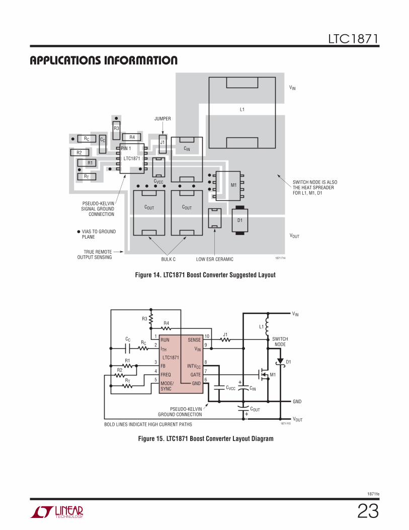
PC Board Layout Checklist
1. In order to minimize switching noise and improve output load regulation, the GND pin of the LTC1871 should be connected directly to 1) the negative terminal of the INTVCC decoupling capacitor, 2) the negative terminal of the output decoupling capacitors, 3) the source of
the power MOSFET or the bottom terminal of the sense
resistor, 4) the negative terminal of the input capacitor
and 5) at least one via to the ground plane immediately
adjacent to Pin 6. The ground trace on the top layer of
the PC board should be as wide and short as possible
to minimize series resistance and inductance.
2. Beware of ground loops in multiple layer PC boards. Try to maintain one central ground node on the board and use the input capacitor to avoid excess input ripple for high output current power supplies. If the ground plane is to be used for high DC currents, choose a path away from the small-signal components.
3. Place the CVCC capacitor immediately adjacent to the INTVCC and GND pins on the IC package. This capaci-tor carries high di/dt MOSFET gate drive currents. A low ESR and ESL 4.7μF ceramic capacitor works well here.
4. The high di/dt loop from the bottom terminal of the output capacitor, through the power MOSFET, through the boost diode and back through the output capacitors
should be kept as tight as possible to reduce inductive ringing. Excess inductance can cause increased stress on the power MOSFET and increase HF noise on the output. If low ESR ceramic capacitors are used on the output to reduce output noise, place these capacitors close to the boost diode in order to keep the series inductance to a minimum.
5. Check the stress on the power MOSFET by measuring its drain-to-source voltage directly across the device terminals (reference the ground of a single scope probe directly to the source pad on the PC board). Beware of inductive ringing which can exceed the maximum specifi ed voltage rating of the MOSFET. If this ringing cannot be avoided and exceeds the maximum rating of the device, either choose a higher voltage device or specify an avalanche-rated power MOSFET. Not all MOSFETs are created equal (some are more equal than others).
6. Place the small-signal components away from high frequency switching nodes. In the layout shown in Figure 14, all of the small-signal components have been placed on one side of the IC and all of the power components have been placed on the other. This also allows the use of a pseudo-Kelvin connection for the signal ground, where high di/dt gate driver currents fl ow out of the IC ground pin in one direction (to the bottom plate of the INTVCC decoupling capacitor) and small-signal currents fl ow in the other direction.
7. If a sense resistor is used in the source of the power MOSFET, minimize the capacitance between the SENSE pin trace and any high frequency switching nodes. The LTC1871 contains an internal leading edge blanking time of approximately 180ns, which should be adequate for most applications.
8. For optimum load regulation and true remote sensing, the top of the output resistor divider should connect independently to the top of the output capacitor (Kelvin connection), staying away from any high dV/dt traces. Place the divider resistors near the LTC1871 in order to keep the high impedance FB node short.
9. For applications with multiple switching power convert-ers connected to the same input supply, make sure
LTC1871
231871fe
APPLICATIONS INFORMATION
Figure 14. LTC1871 Boost Converter Suggested Layout
Figure 15. LTC1871 Boost Converter Layout Diagram
LTC1871
M1
VIN
1871 F14
VOUT
SWITCH NODE IS ALSO THE HEAT SPREADERFOR L1, M1, D1
L1
RT
RC CC
R3
J1
CIN
COUT
CVCC
R1
R2
PSEUDO-KELVINSIGNAL GROUND
CONNECTION
TRUE REMOTEOUTPUT SENSING
VIAS TO GROUND PLANE
R4
PIN 1
COUT
BULK C LOW ESR CERAMIC
JUMPER
D1
RUN
ITH
FB
FREQ
MODE/SYNC
SENSE
VIN
INTVCC
GATE
GND
LTC1871
+
R4
J110
9
8
7
6
1
2
3
4
5
CVCC
PSEUDO-KELVINGROUND CONNECTION
CIN
M1
D1
L1
VIN
GND
1871 F15
VOUT
SWITCHNODE
COUT
RC
R1
RT
BOLD LINES INDICATE HIGH CURRENT PATHS
R2
CC
R3
+
LTC1871
241871fe
APPLICATIONS INFORMATIONthat the input fi lter capacitor for the LTC1871 is not shared with other converters. AC input current from another converter could cause substantial input voltage ripple, and this could interfere with the operation of the LTC1871. A few inches of PC trace or wire (L ≈ 100nH) between the CIN of the LTC1871 and the actual source VIN should be suffi cient to prevent current sharing problems.
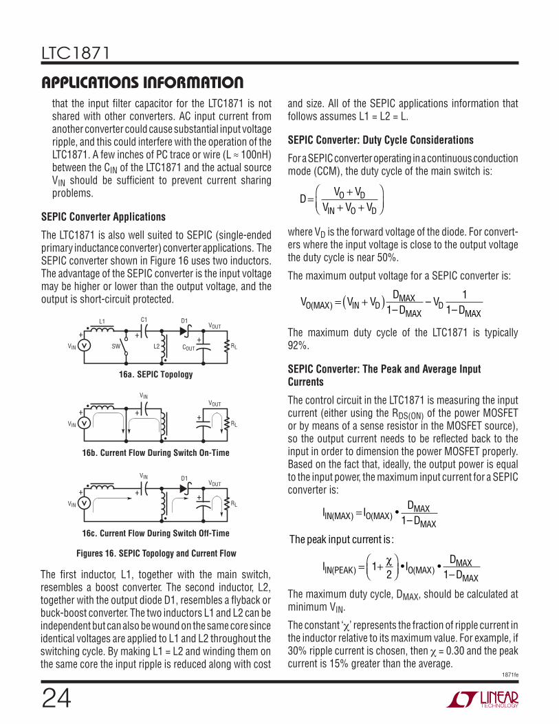
SEPIC Converter Applications
The LTC1871 is also well suited to SEPIC (single-ended primary inductance converter) converter applications. The SEPIC converter shown in Figure 16 uses two inductors. The advantage of the SEPIC converter is the input voltage may be higher or lower than the output voltage, and the output is short-circuit protected.
Figures 16. SEPIC Topology and Current Flow
+
++•
•
•
•
SW L2 COUTRL
VOUT
VIN
C1 D1L1
16a. SEPIC Topology
+
++•
RL
VOUT
VIN
D1
16c. Current Flow During Switch Off-Time
+
++•
RL
VOUT
VIN
VIN
VIN
16b. Current Flow During Switch On-Time
The fi rst inductor, L1, together with the main switch, resembles a boost converter. The second inductor, L2, together with the output diode D1, resembles a fl yback or buck-boost converter. The two inductors L1 and L2 can be independent but can also be wound on the same core since identical voltages are applied to L1 and L2 throughout the switching cycle. By making L1 = L2 and winding them on the same core the input ripple is reduced along with cost
and size. All of the SEPIC applications information that follows assumes L1 = L2 = L.
SEPIC Converter: Duty Cycle Considerations
For a SEPIC converter operating in a continuous conduction mode (CCM), the duty cycle of the main switch is:
D=VO + VD
VIN + VO + VD
where VD is the forward voltage of the diode. For convert-ers where the input voltage is close to the output voltage the duty cycle is near 50%.
The maximum output voltage for a SEPIC converter is:
VO(MAX) = VIN + VD( )
DMAX
1–DMAX– VD
1
1–DMAX
The maximum duty cycle of the LTC1871 is typically 92%.
SEPIC Converter: The Peak and Average Input Currents
The control circuit in the LTC1871 is measuring the input current (either using the RDS(ON) of the power MOSFET or by means of a sense resistor in the MOSFET source), so the output current needs to be refl ected back to the input in order to dimension the power MOSFET properly. Based on the fact that, ideally, the output power is equal to the input power, the maximum input current for a SEPIC converter is:
IIN(MAX) = IO(MAX) •DMAX
1–DMAX
The peak input current is:
IIN(PEAK) = 1+2
•IO(MAX) •DMAX
1–DMAX
The maximum duty cycle, DMAX, should be calculated at minimum VIN.
The constant ‘χ’ represents the fraction of ripple current in the inductor relative to its maximum value. For example, if 30% ripple current is chosen, then χ = 0.30 and the peak current is 15% greater than the average.

LTC1871
251871fe
APPLICATIONS INFORMATIONIt is worth noting here that SEPIC converters that operate at high duty cycles (i.e., that develop a high output volt-age from a low input voltage) can have very high input currents, relative to the output current. Be sure to check that the maximum load current will not overload the input supply.
SEPIC Converter: Inductor Selection
For most SEPIC applications the equal inductor values will fall in the range of 10μH to 100μH. Higher values will reduce the input ripple voltage and reduce the core loss. Lower inductor values are chosen to reduce physical size and improve transient response.
Like the boost converter, the input current of the SEPIC converter is calculated at full load current and minimum input voltage. The peak inductor current can be signifi cantly higher than the output current, especially with smaller in-ductors and lighter loads. The following formulas assume CCM operation and calculate the maximum peak inductor currents at minimum VIN:
IL1(PEAK) = 1+2
•IO(MAX) •VO + VD
VIN(MIN)
IL2(PEAK) = 1+2
•IO(MAX) •VIN(MIN) + VD
VIN(MIN)
The ripple current in the inductor is typically 20% to 40% (i.e., a range of ‘χ’ from 0.20 to 0.40) of the maximum average input current occurring at VIN(MIN) and IO(MAX) and ΔIL1 = ΔIL2. Expressing this ripple current as a function of the output current results in the following equations for calculating the inductor value:
L =VIN(MIN)
IL • f•DMAX
where:
IL = •IO(MAX) •DMAX
1–DMAX
By making L1 = L2 and winding them on the same core, the value of inductance in the equation above is replace by 2L due to mutual inductance. Doing this maintains the same ripple current and energy storage in the inductors. For
example, a Coiltronix CTX10-4 is a 10μH inductor with two windings. With the windings in parallel, 10μH inductance is obtained with a current rating of 4A (the number of turns hasn’t changed, but the wire diameter has doubled). Split-ting the two windings creates two 10μH inductors with a current rating of 2A each. Therefore, substituting 2L yields the following equation for coupled inductors:
L1=L2=
VIN(MIN)
2 • IL • f•DMAX
Specify the maximum inductor current to safely handle IL(PK) specifi ed in the equation above. The saturation current rating for the inductor should be checked at the minimum input voltage (which results in the highest inductor current) and maximum output current.
SEPIC Converter: Power MOSFET Selection
The power MOSFET serves two purposes in the LTC1871: it represents the main switching element in the power path, and its RDS(ON) represents the current sensing element for the control loop. Important parameters for the power MOSFET include the drain-to-source breakdown voltage (BVDSS), the threshold voltage (VGS(TH)), the on-resistance (RDS(ON)) versus gate-to-source voltage, the gate-to-source and gate-to-drain charges (QGS and QGD, respectively), the maximum drain current (ID(MAX)) and the MOSFET’s thermal resistances (RTH(JC) and RTH(JA)).
The gate drive voltage is set by the 5.2V INTVCC low dropout regulator. Consequently, logic-level threshold MOSFETs should be used in most LTC1871 applications. If low input voltage operation is expected (e.g., supplying power from a lithium-ion battery), then sublogic-level threshold MOSFETs should be used.
The maximum voltage that the MOSFET switch must sustain during the off-time in a SEPIC converter is equal to the sum of the input and output voltages (VO + VIN). As a result, careful attention must be paid to the BVDSS specifi cations for the MOSFETs relative to the maximum actual switch voltage in the application. Many logic-level devices are limited to 30V or less. Check the switching waveforms directly across the drain and source terminals of the power MOSFET to ensure the VDS remains below the maximum rating for the device.

LTC1871
261871fe
APPLICATIONS INFORMATIONDuring the MOSFET’s on-time, the control circuit limits the maximum voltage drop across the power MOSFET to about 150mV (at low duty cycle). The peak inductor current is therefore limited to 150mV/RDS(ON). The relationship between the maximum load current, duty cycle and the RDS(ON) of the power MOSFET is:
RDS(ON)
VSENSE(MAX)
IO(MAX)•
1
1+2
• T
•1
VO + VD
VIN(MIN)+1
The VSENSE(MAX) term is typically 150mV at low duty cycle and is reduced to about 100mV at a duty cycle of 92% due to slope compensation, as shown in Figure 8. The constant ‘χ’ in the denominator represents the ripple current in the inductors relative to their maximum current. For example, if 30% ripple current is chosen, then χ = 0.30. The ρT term accounts for the temperature coeffi cient of the RDS(ON) of the MOSFET, which is typically 0.4%/°C. Figure 9 illustrates the variation of normalized RDS(ON) over temperature for a typical power MOSFET.
Another method of choosing which power MOSFET to use is to check what the maximum output current is for a given RDS(ON) since MOSFET on-resistances are available in discrete values.
IO(MAX)
VSENSE(MAX)
RDS(ON)•
1
1+2
• T
•1
VO + VD
VIN(MIN)+1
Calculating Power MOSFET Switching and Conduction Losses and Junction Temperatures
In order to calculate the junction temperature of the power MOSFET, the power dissipated by the device must be known. This power dissipation is a function of the duty cycle, the load current and the junction temperature itself. As a result, some iterative calculation is normally required to determine a reasonably accurate value. Since the controller is using the MOSFET as both a switching and a sensing element, care should be taken to ensure that the converter is capable of delivering the required load current over all operating conditions (load, line and temperature) and for the worst-case specifi cations for VSENSE(MAX) and the RDS(ON) of the MOSFET listed in the manufacturer’s data sheet.
The power dissipated by the MOSFET in a SEPIC converter is:
PFET = IO(MAX) •DMAX
1–DMAX
2
•RDS(ON) •DMAX • T
+ k • VIN(MIN) + VO( )1.85
•IO(MAX) •DMAX
1–DMAX• CRSS • f
The fi rst term in the equation above represents the I2R losses in the device and the second term, the switching losses. The constant k = 1.7 is an empirical factor inversely related to the gate drive current and has the dimension of 1/current.
From a known power dissipated in the power MOSFET, its junction temperature can be obtained using the following formula:
TJ = TA + PFET •RTH(JA)
The RTH(JA) to be used in this equation normally includes the RTH(JC) for the device plus the thermal resistance from the board to the ambient temperature in the enclosure. This value of TJ can then be used to check the original assumption for the junction temperature in the iterative calculation process.
SEPIC Converter: Output Diode Selection
To maximize effi ciency, a fast-switching diode with low forward drop and low reverse leakage is desired. The output diode in a SEPIC converter conducts current during the switch off-time. The peak reverse voltage that the diode must withstand is equal to VIN(MAX) + VO. The average forward current in normal operation is equal to the output current, and the peak current is equal to:
ID(PEAK) = 1+2
•IO(MAX) •VO + VD
VIN(MIN)+1
The power dissipated by the diode is:
PD = IO(MAX) • VD
and the diode junction temperature is:
TJ = TA + PD • RTH(JA)
The RTH(JA) to be used in this equation normally includes the RTH(JC) for the device plus the thermal resistance from the board to the ambient temperature in the enclosure.

LTC1871
271871fe
APPLICATIONS INFORMATIONSEPIC Converter: Output Capacitor Selection
Because of the improved performance of today’s electro-lytic, tantalum and ceramic capacitors, engineers need to consider the contributions of ESR (equivalent series resistance), ESL (equivalent series inductance) and the bulk capacitance when choosing the correct component for a given output ripple voltage. The effects of these three parameters (ESR, ESL, and bulk C) on the output voltage ripple waveform are illustrated in Figure 17 for a typical coupled-inductor SEPIC converter.
The choice of component(s) begins with the maximum acceptable ripple voltage (expressed as a percentage of the output voltage), and how this ripple should be divided between the ESR step and the charging/discharging ΔV. For the purpose of simplicity we will choose 2% for the maximum output ripple, to be divided equally between the ESR step and the charging/discharging ΔV. This percentage ripple will change, depending on the requirements of the application, and the equations provided below can easily be modifi ed.
For a 1% contribution to the total ripple voltage, the ESR of the output capacitor can be determined using the fol-lowing equation:
ESRCOUT0.01• VO
ID(PEAK)
where:
ID(PEAK) = 1+2
•IO(MAX) •VO + VD
VIN(MIN)+1
For the bulk C component, which also contributes 1% to the total ripple:
COUT
IO(MAX)
0.01• VO • f
For many designs it is possible to choose a single capacitor type that satisfi es both the ESR and bulk C requirements for the design. In certain demanding applications, however, the ripple voltage can be improved signifi cantly by con-necting two or more types of capacitors in parallel. For example, using a low ESR ceramic capacitor can minimize the ESR step, while an electrolytic or tantalum capacitor can be used to supply the required bulk C.
Once the output capacitor ESR and bulk capacitance have been determined, the overall ripple voltage waveform should be verifi ed on a dedicated PC board (see Board Layout section for more information on component place-ment). Lab breadboards generally suffer from excessive series inductance (due to inter-component wiring), and these parasitics can make the switching waveforms look signifi cantly worse than they would be on a properly designed PC board.
Figure 17. SEPIC Converter Switching Waveforms
17a. Input Inductor Current
IINIL1
SWON
SWOFF
17b. Output Inductor Current
IOIL2
17c. DC Coupling Capacitor Current
IO
IIN
IC1
17e. Output Ripple Voltage
VOUT(AC)
ΔVESR
RINGING DUE TOTOTAL INDUCTANCE(BOARD + CAP)
ΔVCOUT
17d. Diode Current
IO
ID1

LTC1871
281871fe
APPLICATIONS INFORMATIONThe output capacitor in a SEPIC regulator experiences high RMS ripple currents, as shown in Figure 17. The RMS output capacitor ripple current is:
IRMS(COUT) = IO(MAX) •VO
VIN(MIN)
Note that the ripple current ratings from capacitor manu-facturers are often based on only 2000 hours of life. This makes it advisable to further derate the capacitor or to choose a capacitor rated at a higher temperature than required. Several capacitors may also be placed in parallel to meet size or height requirements in the design.
Manufacturers such as Nichicon, United Chemicon and Sanyo should be considered for high performance through-hole capacitors. The OS-CON semiconductor dielectric capacitor available from Sanyo has the lowest product of ESR and size of any aluminum electrolytic, at a somewhat higher price.
In surface mount applications, multiple capacitors may have to be placed in parallel in order to meet the ESR or RMS current handling requirements of the application. Aluminum electrolytic and dry tantalum capacitors are both available in surface mount packages. In the case of tantalum, it is critical that the capacitors have been surge tested for use in switching power supplies. An excellent choice is AVX TPS series of surface mount tantalum. Also, ceramic capacitors are now available with extremely low ESR, ESL and high ripple current ratings.
SEPIC Converter: Input Capacitor Selection
The input capacitor of a SEPIC converter is less critical than the output capacitor due to the fact that an inductor is in series with the input and the input current waveform is triangular in shape. The input voltage source impedance determines the size of the input capacitor which is typi-cally in the range of 10μF to 100μF. A low ESR capacitor is recommended, although it is not as critical as for the output capacitor.
The RMS input capacitor ripple current for a SEPIC con-verter is:
IRMS(CIN) =
1
12• IL
Please note that the input capacitor can see a very high surge current when a battery is suddenly connected to the input of the converter and solid tantalum capacitors can fail catastrophically under these conditions. Be sure to specify surge-tested capacitors!
SEPIC Converter: Selecting the DC Coupling Capacitor
The coupling capacitor C1 in Figure 16 sees nearly a rectan-gular current waveform as shown in Figure 17. During the switch off-time the current through C1 is IO(VO/VIN) while approximately – IO fl ows during the on-time. This current waveform creates a triangular ripple voltage on C1:
VC1(P P) =
IO(MAX)
C1• f•
VO
VIN + VO + VD
The maximum voltage on C1 is then:
VC1(MAX) = VIN +
VC1(P P)
2
which is typically close to VIN(MAX). The ripple current through C1 is:
IRMS(C1) = IO(MAX) •VO + VD
VIN(MIN)
The value chosen for the DC coupling capacitor normally
starts with the minimum value that will satisfy 1) the RMS
current requirement and 2) the peak voltage requirement
(typically close to VIN). Low ESR ceramic and tantalum
capacitors work well here.
SEPIC Converter Design Example
The design example given here will be for the circuit shown in Figure 18. The input voltage is 5V to 15V and the output is 12V at a maximum load current of 1.5A (2A peak).
1. The duty cycle range is:
D=VO + VD
VIN + VO + VD= 45.5% to 71.4%
2. The operating mode chosen is pulse skipping, so the MODE/SYNC pin is shorted to INTVCC.
LTC1871
291871fe
APPLICATIONS INFORMATION3. The operating frequency is chosen to be 300kHz to
reduce the size of the inductors; the resistor from the FREQ pin to ground is 80k.
4. An inductor ripple current of 40% is chosen, so the peak input current (which is also the minimum saturation current) is:
IL1(PEAK) = 1+2
•IO(MAX) •VO + VD
VIN(MIN)
= 1+0.4
2• 1.5 •
12+ 0.5
5= 4.5A
The inductor ripple current is:
IL = •IO(MAX) •DMAX
1–DMAX
= 0.4 • 1.5 •0.714
1– 0.714=1.5A
And so the inductor value is:
L =
VIN(MIN)
2 • IL • f•DMAX =
5
2 • 1.5 • 300k• 0.714= 4μH
The component chosen is a BH Electronics BH510-1007, which has a saturation current of 8A.
5. With an minimum input voltage of 5V, only logic-level power MOSFETs should be considered. Because the maximum duty cycle is 71.4%, the maximum SENSE pin threshold voltage is reduced from its low duty cycle typical value of 150mV to approximately 120mV. Assuming a MOSFET junction temperature of 125°C, the room temperature MOSFET RDS(ON) should be less than:
RDS(ON)
VSENSE(MAX)
IO(MAX)•
1
1+2
• T
•1
VO + VD
VIN(MIN)+1
=0.12
1.5•
1
1.2 • 1.5•
1
12.5
5+1
=12.7m
For a SEPIC converter, the switch BVDSS rating must be greater than VIN(MAX) + VO, or 27V. This comes close to an IRF7811W, which is rated to 30V, and has a maximum room temperature RDS(ON) of 12mΩ at VGS = 4.5V.
6. The diode for this design must handle a maximum DC output current of 2A and be rated for a minimum reverse voltage of VIN + VOUT, or 27V. A 3A, 40V diode from International Rectifi er (30BQ040) is chosen for its small size, relatively low forward drop and acceptable reverse leakage at high temp.
7. The output capacitor usually consists of a high valued bulk C connected in parallel with a lower valued, low ESR ceramic. Based on a maximum output ripple voltage of 1%, or 120mV, the bulk C needs to be greater than:
COUT
IOUT(MAX)
0.01• VOUT • f=
1.5A
0.01• 12V • 300kHz= 41μF
The RMS ripple current rating for this capacitor needs to exceed:
IRMS(COUT) IO(MAX) •VO
VIN(MIN)=
1.5A •12V
5V= 2.3A
To satisfy this high RMS current demand, two 47μF Kemet capacitors (T495X476K020AS) are required. As a result, the output ripple voltage is a low 50mV to 60mV. In parallel with these tantalums, two 10μF, low ESR (X5R) Taiyo Yuden ceramic capacitors (TMK432BJ106MM) are added for HF noise reduction. Check the output ripple with a single oscilloscope probe connected directly across the output capacitor terminals, where the HF switching currents fl ow.
8. The choice of an input capacitor for a SEPIC converter depends on the impedance of the source supply and the amount of input ripple the converter will safely toler-ate. For this particular design and lab setup, a single 47μF Kemet tantalum capacitor (T495X476K020AS) is adequate. As with the output node, check the input ripple with a single oscilloscope probe connected across the input capacitor terminals. If any HF switching noise is observed it is a good idea to decouple the input with a low ESR, X5R ceramic capacitor as close to the VIN and GND pins as possible.

LTC1871
301871fe
APPLICATIONS INFORMATION9. The DC coupling capacitor in a SEPIC converter is cho-
sen based on its RMS current requirement and must be rated for a minimum voltage of VIN plus the AC ripple voltage. Start with the minimum value which satisfi es the RMS current requirement and then check the ripple voltage to ensure that it doesn’t exceed the DC rating.
IRMS(CI) IO(MAX) •VO + VD
VIN(MIN)
=1.5A •12V + 0.5V
5V= 2.4A
Figure 18a. 4.5V to 15V Input, 12V/2A Output SEPIC Converter
Figure 18b. SEPIC Effi ciency vs Output Current
RUN
ITH
FB
FREQ
MODE/SYNC
SENSE
VIN
INTVCC
GATE
GND
1
2
3
4
5
10
9
8
7
6
LTC1871
RT80.6k1%
R112.1k
1%R2105k
1%
R31M
CVCC4.7μFX5R
CIN47μF
M1
CIN, COUT1: KEMET T495X476K020ASCDC, COUT2: TAIYO YUDEN TMK432BJ106MMD1: INTERNATIONAL RECTIFIER 30BQ040
D1
•
•
L1*
L2*
RC33k
CC16.8nF
CC247pF
COUT147μF20V×2
VIN4.5V to 15V
VOUT12V1.5A(2A PEAK)
GND1871 F018a
+COUT210μF25VX5R×2
L1, L2: BH ELECTRONICS BH510-1007 (*COUPLED INDUCTORS)M1: INTERNATIONAL RECTIFIER IRF7811W
CDC10μF25VX5R
+
OUTPUT CURRENT (A)
50
EFF
ICIE
NC
Y (
%)
55
60
90
85
80
75
70
65
95
0.001 0.1 1 10
1871 F18b
450.01
100
VIN = 4.5V
VIN = 15V
VIN = 12V
VO = 12VMODE = INTVCC
For this design a single 10μF, low ESR (X5R) Taiyo Yuden ceramic capacitor (TMK432BJ106MM) is adequate.

LTC1871
311871fe
APPLICATIONS INFORMATION
Figure 19. LTC1871 SEPIC Converter Load Step Response
VOUT (AC)200mV/DIV
IOUT0.5A/DIV
50μs/DIV1871 F19
VIN = 15VVOUT = 12V
VOUT (AC)200mV/DIV
IOUT0.5A/DIV
50μs/DIV
VIN = 4.5VVOUT = 12V
TYPICAL APPLICATIONS2.5V to 3.3V Input, 5V/2A Output Boost Converter
Output Effi ciency at 2.5V and 3.3V Input
RUN
ITH
FB
FREQ
MODE/SYNC
SENSE
VIN
INTVCC
GATE
GND
1
2
3
4
5
10
9
8
7
6
LTC1871
RT80.6k1%
R112.1k
1%R237.4k
1%
CVCC4.7μFX5R
CIN47μF6.3V
M1
CIN: SANYO POSCAP 6TPA47MCOUT1: SANYO POSCAP 6TPB150MCOUT2: TAIYO YUDEN JMK316BJ106MLCVCC: TAIYO YUDEN LMK316BJ475ML
D1
L11.8μH
RC22k
CC16.8nF
CC247pF
COUT1150μF6.3V×2
VIN2.5V to 3.3V
VOUT5V2A
GND1871 TA01a
+COUT210μF6.3VX5R×2
D1: INTERNATIONAL RECTIFIER 30BQ015L1: TOKO DS104C2 B952AS-1R8NM1: SILICONIX/VISHAY Si9426
+
OUTPUT CURRENT (A)
65
EFF
ICIE
NC
Y (
%)
95
100
60
55
90
75
85
80
70
0.001 0.1 1 10
1871 TA01b
500.01

LTC1871
321871fe
TYPICAL APPLICATIONS18V to 27V Input, 28V Output, 400W 2-Phase, Low Ripple, Synchronized RF Base Station Power Supply (Boost)
5V to 12V Input, ±12V/0.2A Output SEPIC Converter with Undervoltage Lockout
RUN
ITH
FB
FREQ
MODE/SYNC
SENSE
VIN
INTVCC
GATE
GND
1
2
3
4
5
10
9
8
7
6
LTC1871
RT1150k5%
RS10.007Ω1W
EXT CLOCKINPUT (200kHz)
R28.45k1%
CVCC14.7μFX5R
CIN22.2μF35VX5R
M1
D1
L25.6μH
L5*0.3μH
CC147pF
CFB147pF
VIN18V to 27V
GND
VOUT28V14A
1871 TA04
COUT12.2μF35VX5R×3
COUT2330μF50V
CIN1: SANYO 50MV330AX CIN2, 3: TAIYO YUDEN GMK325BJ225MNCOUT2, 4, 5: SANYO 50MV330AXCOUT1, 3, 6: TAIYO YUDEN GMK325BJ225MNCVCC1, 2: TAIYO YUDEN LMK316BJ475ML
L1 TO L4: SUMIDA CEP125-5R6MC-HD L5: SUMIDA CEP125-0R3NC-NDD1, D2: ON SEMICONDUCTOR MBR2045CTM1, M2: INTERNATIONAL RECTIFIER IRLZ44NS
R193.1k
1%
L15.6μH
*L5, COUT5 AND COUT6 ARE ANOPTIONAL SECONDARYFILTER TO REDUCEOUTPUT RIPPLE FROM<500mVP-P TO <100mVP-P
+
COUT5*330μF
50V×4 COUT6*
2.2μF35VX5R
CIN1330μF50V
RUN
ITH
FB
FREQ
MODE/SYNC
SENSE
VIN
INTVCC
GATE
GND
1
2
3
4
5
10
9
8
7
6
LTC1871
RT2150k5%
R312.1k1%
RC22k
R4261k
1%
CVCC24.7μFX5R
CIN32.2μF35VX5R
M2
D2
L45.6μH
CC247pF
CC36.8nF
CFB247pF
COUT32.2μF35VX5R×3
COUT4330μF50V
L35.6μH
+
+
RS20.007Ω1W
+
RUN
ITH
FB
FREQ
MODE/SYNC
SENSE
VIN
INTVCC
GATE
GND
1
2
3
4
5
10
9
8
7
6
LTC1871
RT60.4k1%
RS0.02Ω
R4127Ω
1%
R254.9k1%
R31.10k
1%
CVCC4.7μF10VX5R
CIN11μF16VX5R
M1
D1
L1*
•
RC22k
CC16.8nF
CC2100pF
CDC14.7μF16VX5R
VIN5V to 12V
VOUT112V0.4A
GND
VOUT2–12V0.4A
1871 TA03
COUT14.7μF16VX5R×3
COUT24.7μF16VX5R×3
D1, D2: MBS120T3L1 TO L3: COILTRONICS VP1-0076 (*COUPLED INDUCTORS)M1: SILICONIX/VISHAY Si4840
R1127k
1%
CIN247μF16VAVX
CDC24.7μF
16VX5R
+
L2*
L3*
D2
•
•
NOTE: 1. VIN UVLO+ = 4.47V VIN UVLO– = 4.14V

LTC1871
331871fe
TYPICAL APPLICATIONS4.5V to 28V Input, 5V/2A Output SEPIC Converter with Undervoltage Lockout and Soft-Start
Soft-Start Load Step Response at VIN = 4.5V
Load Step Response at VIN = 28V
RUN
ITH
FB
FREQ
MODE/SYNC
SENSE
VIN
INTVCC
GATE
GND
1
2
3
4
5
10
9
8
7
6
LTC1871
RT162k1%
C21μFX5R
NOTES: 1. VIN UVLO+ = 4.17V VIN UVLO– = 3.86V 2. SOFT-START dVOUT/dt = 5V/6ms
R449.9k
1%R3154k
1%
Q1
R1115k
1%R254.9k1%
CVCC4.7μF10VX5R
CIN12.2μF35VX5R
CIN222μF35V
M1
D1
•
•
L1*
L2*
RC12k
CC18.2nF
C14.7nF
CC247pF
R6750Ω
R5100Ω
COUT1330μF6.3V
VIN4.5V to 28V
VOUT5V2A(3A TO 4A PEAK)
GND1871 TA02a
+
COUT222μF6.3VX5R
CDC2.2μF25VX5R×3
+
CIN1, CDC: TAIYO YUDEN GMK325BJ225MNCIN2: AVX TPSE226M035R0300COUT1: SANYO 6TPB330MCOUT2: TAIYO YUDEN JMK325BJ226MNCVCC: LMK316BJ475ML
D1: INTERNATIONAL RECTIFIER 30BQ040L1, L2: BH ELECTRONICS BH510-1007 (*COUPLED INDUCTORS)M1: SILICONIX/VISHAY Si4840Q1: PHILIPS BC847BF
VOUT1V/DIV
1ms/DIV1871 TA02b
VOUT100mV/DIV
(AC)
2.2A
0.5A
250μs/DIV1871 TA02c
IOUT1A/DIV
(DC)
VOUT100mV/DIV
(AC)
2.2A
0.5A
250μs/DIV1871 TA02d
IOUT1A/DIV
(DC)

LTC1871
341871fe
TYPICAL APPLICATIONS5V to 15V Input, –5V/5A Output Positive-to-Negative Converter with Undervoltage Lockout and Level-Shifted Feedback
RUN
ITH
FB
FREQ
MODE/SYNC
SENSE
VIN
INTVCC
GATE
GND
1
2
3
4
5
10
9
8
7
6
LTC1871
RT80.6k1%
R1154k
1%R2
68.1k1%
C11nF
CVCC4.7μF10VX5R
C210nF
R410k1%
R540.2k1%R3
10k1%
4
3
2
6
1
CIN47μF16VX5R
M1
CIN: TDK C5750X5R1C476MCDC: TDK C5750X7R1E226MCOUT: TDK C5750X5R0J107MCVCC: TAIYO YUDEN LMK316BJ475ML
D1
• •
L1* L2*
RC10k
CC110nF
CC2330pF
VIN5V to 15V
VOUT–5V5A
GND
1871 TA05
COUT100μF6.3VX5R×2
D1: ON SEMICONDUCTOR MBRB2035CTL1, L2: COILTRONICS VP5-0053 (*3 WINDINGS IN PARALLEL FOR THE PRIMARY, 3 IN PARALLEL FOR SECONDARY)M1: INTERNATIONAL RECTIFIER IRF7822
CDC22μF25VX7R
–
+LT1783

LTC1871
351871fe
Information furnished by Linear Technology Corporation is believed to be accurate and reliable. However, no responsibility is assumed for its use. Linear Technology Corporation makes no representa-tion that the interconnection of its circuits as described herein will not infringe on existing patent rights.
PACKAGE DESCRIPTIONMS Package
10-Lead Plastic MSOP(Reference LTC DWG # 05-08-1661 Rev E)
MSOP (MS) 0307 REV E
0.53 ± 0.152(.021 ± .006)
SEATINGPLANE
0.18(.007)
1.10(.043)MAX
0.17 – 0.27(.007 – .011)
TYP
0.86(.034)REF
0.50(.0197)
BSC
1 2 3 4 5
4.90 ± 0.152(.193 ± .006)
0.497 ± 0.076(.0196 ± .003)
REF8910 7 6
3.00 ± 0.102(.118 ± .004)
(NOTE 3)
3.00 ± 0.102(.118 ± .004)
(NOTE 4)
NOTE:1. DIMENSIONS IN MILLIMETER/(INCH)2. DRAWING NOT TO SCALE3. DIMENSION DOES NOT INCLUDE MOLD FLASH, PROTRUSIONS OR GATE BURRS. MOLD FLASH, PROTRUSIONS OR GATE BURRS SHALL NOT EXCEED 0.152mm (.006") PER SIDE4. DIMENSION DOES NOT INCLUDE INTERLEAD FLASH OR PROTRUSIONS. INTERLEAD FLASH OR PROTRUSIONS SHALL NOT EXCEED 0.152mm (.006") PER SIDE5. LEAD COPLANARITY (BOTTOM OF LEADS AFTER FORMING) SHALL BE 0.102mm (.004") MAX
0.254(.010)
0° – 6° TYP
DETAIL “A”
DETAIL “A”
GAUGE PLANE
5.23(.206)MIN
3.20 – 3.45(.126 – .136)
0.889 ± 0.127(.035 ± .005)
RECOMMENDED SOLDER PAD LAYOUT
0.305 ± 0.038(.0120 ± .0015)
TYP
0.50(.0197)
BSC
0.1016 ± 0.0508(.004 ± .002)

LTC1871
361871fe
Linear Technology Corporation1630 McCarthy Blvd., Milpitas, CA 95035-7417 (408) 432-1900 ● FAX: (408) 434-0507 ● www.linear.com © LINEAR TECHNOLOGY CORPORATION 2001
LT 0108 REV E • PRINTED IN USA
RELATED PARTS
TYPICAL APPLICATIONHigh Power SLIC Supply with Undervoltage Lockout
(Also See the LTC3704 Data Sheet)
+
RUN
ITH
FB
FREQ
MODE/SYNC
SENSE
VIN
INTVCC
GATE
GND
LTC1871
RT120k
f = 200kHz
*COILTRONICS VP5-0155 (PRIMARY = 3 WINDINGS IN PARALLEL)
C14.7μFX5R
+ CIN220μF16VTPS
C310μF25VX5R
IRL2910
RS0.012Ω
C80.1μF
D310BQ060
5
•
•
VIN7V TO 12V
T1*1, 2, 3
RC82k
CC11nF
CC2100pF
CR1nF
R149.9k1%
R2150k1%
D410BQ060
6
•
D210BQ060
4
•
C410μF25VX5R
COUT3.3μF100V
GND
VOUT1–24V200mA
VOUT2–72V200mA
C510μF25VX5R
4
3
1871 TA06
2
6
110k
RF110k1%
RF2196k1%
C24.7μF50VX5R
–
+LT1783
PART NUMBER DESCRIPTION COMMENTS
LT®1619 Current Mode PWM Controller 300kHz Fixed Frequency, Boost, SEPIC, Flyback Topology
LTC1624 Current Mode DC/DC Controller SO-8; 300kHz Operating Frequency; Buck, Boost, SEPIC Design;VIN Up to 36V
LTC1700 No RSENSE Synchronous Step-Up Controller Up to 95% Effi ciency, Operation as Low as 0.9V Input
LTC1871-7 Wide Input Range Controller No RSENSE, 7V Gate Drive, Current Mode Control
LTC1872 SOT-23 Boost Controller Delivers Up to 5A, 550kHz Fixed Frequency, Current Mode
LT1930 1.2MHz, SOT-23 Boost Converter Up to 34V Output, 2.6V ≤ VIN ≤ 16V, Miniature Design
LT1931 Inverting 1.2MHz, SOT-23 Converter Positive-to-Negative DC/DC Conversion, Miniature Design
LTC3401/LTC3402 1A/2A 3MHz Synchronous Boost Converters Up to 97% Effi ciency, Very Small Solution, 0.5V ≤ VIN ≤ 5V
LTC3704 Positive-to-Negative DC/DC Controller No RSENSE, Current Mode Control, 50kHz to 1MHz
LT3782 2-Phase Step-Up DC/DC Controller 6V ≤ VIN ≤ 40V; 4A Gate Drive, 150kHz to 500kHz