LT1933 Switching Regulator in SOT-23 and DFN Packages...
20
LT1933 1 1933fe TYPICAL APPLICATION FEATURES APPLICATIONS DESCRIPTION 600mA, 500kHz Step-Down Switching Regulator in SOT-23 and DFN Packages The LT ® 1933 is a current mode PWM step-down DC/DC converter with an internal 0.75A power switch, packaged in a tiny 6-lead SOT-23. The wide input range of 3.6V to 36V makes the LT1933 suitable for regulating power from a wide variety of sources, including unregulated wall transformers, 24V industrial supplies and automotive batteries. Its high operating frequency allows the use of tiny, low cost inductors and ceramic capacitors, resulting in low, predictable output ripple. Cycle-by-cycle current limit provides protection against shorted outputs, and soft-start eliminates input current surge during start up. The low current (<2μA) shutdown provides output disconnect, enabling easy power manage- ment in battery-powered systems. L, LT, LTC, LTM, Linear Technology and the Linear logo are registered trademarks of Linear Technology Corporation. ThinSOT is a trademark of Linear Technology Corporation. All other trademarks are the property of their respective owners. 3.3V Step-Down Converter n Wide Input Range: 3.6V to 36V n 5V at 600mA from 16V to 36V Input n 3.3V at 600mA from 12V to 36V Input n 5V at 500mA from 6.3V to 36V Input n 3.3V at 500mA from 4.5V to 36V Input n Fixed Frequency 500kHz Operation n Uses Tiny Capacitors and Inductors n Soft-Start n Internally Compensated n Low Shutdown Current: <2μA n Output Adjustable Down to 1.25V n Low Profile (1mm) SOT-23 (ThinSOT™) and (2mm × 3mm × 0.75mm) 6-Pin DFN Packages n Automotive Battery Regulation n Industrial Control Supplies n Wall Transformer Regulation n Distributed Supply Regulation n Battery-Powered Equipment Efficiency V IN 4.5V TO 36V OFF ON 0.1μF 22μH 1N4148 MBRM140 10k 16.5k 22μF 1933 TA01a 2.2μF V OUT 3.3V/500mA V IN BOOST GND FB SHDN SW LT1933 LOAD CURRENT (mA) 0 90 95 300 400 1933 TA01b 85 80 100 200 600 500 75 70 65 EFFICIENCY (%) V IN = 12V V OUT = 5V V OUT = 3.3V Downloaded from Elcodis.com electronic components distributor
Transcript of LT1933 Switching Regulator in SOT-23 and DFN Packages...

LT1933
11933fe
TYPICAL APPLICATION
FEATURES
APPLICATIONS
DESCRIPTION
600mA, 500kHz Step-Down Switching Regulator in
SOT-23 and DFN Packages
The LT®1933 is a current mode PWM step-down DC/DC converter with an internal 0.75A power switch, packaged in a tiny 6-lead SOT-23. The wide input range of 3.6V to 36V makes the LT1933 suitable for regulating power from a wide variety of sources, including unregulated wall transformers, 24V industrial supplies and automotive batteries. Its high operating frequency allows the use of tiny, low cost inductors and ceramic capacitors, resulting in low, predictable output ripple.
Cycle-by-cycle current limit provides protection against shorted outputs, and soft-start eliminates input current surge during start up. The low current (<2μA) shutdown provides output disconnect, enabling easy power manage-ment in battery-powered systems.L, LT, LTC, LTM, Linear Technology and the Linear logo are registered trademarks of Linear Technology Corporation. ThinSOT is a trademark of Linear Technology Corporation. All other trademarks are the property of their respective owners.
3.3V Step-Down Converter
n Wide Input Range: 3.6V to 36Vn 5V at 600mA from 16V to 36V Inputn 3.3V at 600mA from 12V to 36V Inputn 5V at 500mA from 6.3V to 36V Inputn 3.3V at 500mA from 4.5V to 36V Inputn Fixed Frequency 500kHz Operationn Uses Tiny Capacitors and Inductorsn Soft-Startn Internally Compensatedn Low Shutdown Current: <2μAn Output Adjustable Down to 1.25Vn Low Profi le (1mm) SOT-23 (ThinSOT™) and
(2mm × 3mm × 0.75mm) 6-Pin DFN Packages
n Automotive Battery Regulationn Industrial Control Suppliesn Wall Transformer Regulationn Distributed Supply Regulationn Battery-Powered Equipment
Effi ciency
VIN4.5V TO 36V
OFF ON
0.1μF22μH
1N4148
MBRM140
10k
16.5k
22μF
1933 TA01a
2.2μF
VOUT3.3V/500mA
VIN BOOST
GND FB
SHDN SW
LT1933
LOAD CURRENT (mA)
0
90
95
300 400
1933 TA01b
85
80
100 200 600500
75
70
65
EFF
ICIE
NC
Y (
%)
VIN = 12V
VOUT = 5V
VOUT = 3.3V
Downloaded from Elcodis.com electronic components distributor
LT1933
21933fe
ABSOLUTE MAXIMUM RATINGS
Input Voltage (VIN) ..................................... –0.4V to 36VBOOST Pin Voltage ...................................................43VBOOST Pin Above SW Pin .........................................20VSHDN Pin ................................................... –0.4V to 36VFB Voltage .................................................... –0.4V to 6VOperating Temperature Range (Note 2)LT1933E ...................................................–40°C to 85°C
(Note 1)
TOP VIEW
FB
GND
SHDN
BOOST
VIN
SW
DCB PACKAGE6-LEAD (2mm × 3mm) PLASTIC DFN
4
57
6
3
2
1
θJA = 73.5°C/W, θJC = 12°C/WEXPOSED PAD (PIN 7) IS GND, MUST BE SOLDERED TO PCB
BOOST 1
GND 2
FB 3
6 SW
5 VIN
4 SHDN
TOP VIEW
S6 PACKAGE6-LEAD PLASTIC TSOT-23
θJA = 165°C/W, θJC = 102°C/W
PIN CONFIGURATION
ORDER INFORMATIONLEAD FREE FINISH TAPE AND REEL PART MARKING PACKAGE DESCRIPTION TEMPERATURE RANGE
LT1933IDCB#PBF LT1933IDCB#TRPBF LCGM 6-Lead (2mm × 3mm) Plastic DFN –40°C to 125°C
LT1933HDCB#PBF LT1933HDCB#TRPBF LCGN 6-Lead (2mm × 3mm) Plastic DFN –40°C to 150°C
LT1933ES6#PBF LT1933ES6#TRPBF LTAGN 6-Lead Plastic TSOT-23 –40°C to 85°C
LT1933IS6#PBF LT1933IS6#TRPBF LTAGP 6-Lead Plastic TSOT-23 –40°C to 125°C
LT1933HS6#PBF LT1933HS6#TRPBF LTDDQ 6-Lead Plastic TSOT-23 –40°C to 150°C
LEAD BASED FINISH TAPE AND REEL PART MARKING PACKAGE DESCRIPTION TEMPERATURE RANGE
LT1933IDCB LT1933IDCB#TR LCGM 6-Lead (2mm × 3mm) Plastic DFN –40°C to 125°C
LT1933HDCB LT1933HDCB#TR LCGN 6-Lead (2mm × 3mm) Plastic DFN –40°C to 150°C
LT1933ES6 LT1933ES6#TR LTAGN 6-Lead Plastic TSOT-23 –40°C to 85°C
LT1933IS6 LT1933IS6#TR LTAGP 6-Lead Plastic TSOT-23 –40°C to 125°C
LT1933HS6 LT1933HS6#TR LTDDQ 6-Lead Plastic TSOT-23 –40°C to 150°C
Consult LTC Marketing for parts specifi ed with wider operating temperature ranges.
For more information on lead free part marking, go to: http://www.linear.com/leadfree/ For more information on tape and reel specifi cations, go to: http://www.linear.com/tapeandreel/
LT1933I .................................................. –40°C to 125°CLT1933H ................................................ –40°C to 150°CMaximum Junction TemperatureLT1933E, LT1933I ................................................. 125°CLT1933H ............................................................... 150°CStorage Temperature Range .................. –65°C to 150°CLead Temperature, S6 Package
(Soldering, 10 sec) ............................................ 300°C
Downloaded from Elcodis.com electronic components distributor
LT1933
31933fe
ELECTRICAL CHARACTERISTICS
Note 1: Stresses beyond those listed under Absolute Maximum Ratings
may cause permanent damage to the device. Exposure to any Absolute
Maximum Rating condition for extended periods may affect device
reliability and lifetime.
Note 2: The LT1933E is guaranteed to meet performance specifi cations
from 0°C to 70°C. Specifi cations over the –40°C to 85°C operating
temperature range are assured by design, characterization and correlation
with statistical process controls. The LT1933I specifi cations are
PARAMETER CONDITIONS MIN TYP MAX UNITS
Undervoltage Lockout 3.35 3.6 V
Feedback Voltage l 1.225 1.245 1.265 V
FB Pin Bias Current VFB = Measured VREF + 10mV (Note 4) l 40 120 nA
Quiescent Current Not Switching 1.6 2.5 mA
Quiescent Current in Shutdown VSHDN = 0V 0.01 2 μA
Reference Line Regulation VIN = 5V to 36V 0.01 %/V
Switching Frequency VFB = 1.1V 400 500 600 kHz
VFB = 0V 55 kHz
Maximum Duty Cycle l 88 94 %
Switch Current Limit (Note 3) 0.75 1.05 A
Switch VCESAT ISW = 400mA, S6 PackageISW = 400mA, DCB6 Package
370370
500 mVmV
Switch Leakage Current 2 μA
Minimum Boost Voltage Above Switch ISW = 400mA 1.9 2.3 V
BOOST Pin Current ISW = 400mA 18 25 mA
SHDN Input Voltage High 2.3 V
SHDN Input Voltage Low 0.3 V
SHDN Bias Current VSHDN = 2.3V (Note 5)VSHDN = 0V
340.01
500.1
μAμA
The l denotes the specifi cations which apply over the full operating temperature range, otherwise specifi cations are at TA = 25°C. VIN = 12V, VBOOST = 17V, unless otherwise noted. (Note 2)
guaranteed over the –40°C to 125°C temperature range. The LT1933H
specifi cations are guaranteed over the –40°C to 150°C temperature range.
Note 3: Current limit guaranteed by design and/or correlation to static test.
Slope compensation reduces current limit at higher duty cycle.
Note 4: Current fl ows out of pin.
Note 5: Current fl ows into pin.
Downloaded from Elcodis.com electronic components distributor

LT1933
41933fe
TYPICAL PERFORMANCE CHARACTERISTICS
Effi ciency, VOUT = 5V Effi ciency, VOUT = 3.3V Switch Current Limit
Maximum Load Current Maximum Load Current Switch Voltage Drop
Feedback Voltage Undervoltage Lockout Switching Frequency
LOAD CURRENT (mA)
0
80
90
100
300 400
1933 G01
70
100 200 60050060
EFF
ICIE
NC
Y (
%)
VIN = 24V
VIN = 12V
TA = 25°CVOUT = 5V
D1 = MBRM140L1 = Toko D53LCB 33μH
LOAD CURRENT (mA)
0
80
90
100
300 400
1933 G02
70
100 200 60050060
EFF
ICIE
NC
Y (
%)
VIN = 24V
VIN = 12V
VIN = 5V
TA = 25°CVOUT = 3.3V
D1 = MBRM140L1 = Toko D53LCB 22μH
DUTY CYCLE (%)
0
SW
ITC
H C
UR
REN
T L
IMIT
(m
A)
600
800
1200
1000
80
1933 G03
400
200
020 40 60 100
MINIMUM
TYPICAL
TA = 25°C
INPUT VOLTAGE (V)
0
LO
AD
CU
RR
EN
T (
mA
)
600
700
20
1933 G04
500
4005 10 15 3025
800
L = 22μH
L = 33μH
TA = 25°CVOUT = 5V
INPUT VOLTAGE (V)
0
LO
AD
CU
RR
EN
T (
mA
)
600
700
20
1933 G05
500
4005 10 15 3025
800
L = 22μH
L = 15μH
TA = 25°CVOUT = 3.3V
SWITCH CURRENT (A)
00
SW
ITC
H V
OLT
AG
E (
mV
)
100
200
300
400
600
500
0.2 0.4
1933 G06
0.60.1 0.3 0.5
TA = 85°C
TA = 25°C
TA = –40°C
TEMPERATURE (°C)
FEED
BA
CK
VO
LTA
GE (
V)
1.260
1.255
1.250
1.240
1.230
1.245
1.235
1933 G07
–50 –25 0 25 50 75 100 150125
TEMPERATURE (°C)
UV
LO
(V
)
3.8
3.6
3.4
3.2
3.0
1933 G08
–50 –25 0 25 50 75 100 150125
TEMPERATURE (°C)
SW
ITC
HIN
G F
REQ
UEN
CY
(kH
z)
600
550
500
450
400
1933 G09
–50 –25 0 25 50 75 100 150125
Downloaded from Elcodis.com electronic components distributor
LT1933
51933fe
TYPICAL PERFORMANCE CHARACTERISTICS
Frequency Foldback Soft-Start SHDN Pin Current
Typical Minimum Input Voltage Typical Minimum Input Voltage Switch Current Limit
Operating WaveformsOperating Waveforms, Discontinuous Mode
FB PIN VOLTAGE (V)
0.0
SW
ITC
HIN
G F
REQ
UEN
CY
(kH
z)
700
600
300
100
400
500
200
00.5
1933 G10
1.0 1.5
TA = 25°C
SHDN PIN VOLTAGE (V)
0
SW
ITC
H C
UR
REN
T L
IMIT
(A
)
1.4
1.2
0.6
0.2
0.8
1.0
0.4
01
1933 G11
2 3 4
TA = 25°CDC = 30%
0
SHDN
PIN
CU
RR
EN
T (
μA
)
200
150
50
100
04
1933 G12
8 12 16
SHDN PIN VOLTAGE (V)
TA = 25°C
LOAD CURRENT (mA)
5
INP
UT V
OLTA
GE (
V)
6
7
8
1933 G13
4
VOUT = 5VTA = 25°CL = 33μH
TO START
TO RUN
1 10 100
LOAD CURRENT (mA)
4.5
INP
UT V
OLTA
GE (
V)
5.0
5.5
6.0
1933 G14
3.0
3.5
4.0
VOUT = 3.3VTA = 25°CL = 22μH
TO START
TO RUN
1 10 100
TEMPERATURE (°C)
–50
SW
ITC
H C
UR
REN
T L
IMIT
(A
)
1.4
1.2
1.0
0.6
0
0.2
0.8
0.4
–25 0 25
1933 G15
50 75 100 150125
VIN = 12V, VOUT = 3.3V, IOUT = 400mA,L = 22μH, COUT = 22μF
1933 G16
VOUT 10mV/DIV
IL 200mA/DIV
VOUT11.8V
VOUT21.2V
VSW 10V/DIV
VIN = 12V, VOUT = 3.3V, IOUT = 20mA,L = 22μH, COUT = 22μF
1933 G17
VOUT 10mV/DIV
IL 200mA/DIV
VOUT11.8V
VOUT21.2V
VSW 10V/DIV
Downloaded from Elcodis.com electronic components distributor

LT1933
61933fe
PIN FUNCTIONSBOOST (Pin 1): The BOOST pin is used to provide a drive voltage, higher than the input voltage, to the internal bipolar NPN power switch.
GND (Pin 2/Pin 5 and Exposed Pad, Pin 7): Tie the GND pin to a local ground plane below the LT1933 and the circuit components. Return the feedback divider to this pin.
FB (Pin 3/Pin 6): The LT1933 regulates its feedback pin to 1.245V. Connect the feedback resistor divider tap to this pin. Set the output voltage according to VOUT = 1.245V (1 + R1/R2). A good value for R2 is 10k.
SHDN (Pin 4): The SHDN pin is used to put the LT1933 in shutdown mode. Tie to ground to shut down the LT1933. Tie to 2.3V or more for normal operation. If the shutdown feature is not used, tie this pin to the VIN pin. SHDN also provides a soft-start function; see the Applications Infor-mation section.
VIN (Pin 5/Pin 2): The VIN pin supplies current to the LT1933’s internal regulator and to the internal power switch. This pin must be locally bypassed.
SW (Pin 6): The SW pin is the output of the internal power switch. Connect this pin to the inductor, catch diode and boost capacitor.
(SOT-23/DFN)
BLOCK DIAGRAM
ΣR
DRIVER Q1S
OSC
SLOPECOMP
FREQUENCYFOLDBACK
INT REGANDUVLO
VCgm
1.245V
1933 BD
Q
Q
BOOST
SW
FB
R2 R1
VOUT
L1
D2
C3
C1D1
VIN
C2
VIN
ON OFF
GND
C4
R3
SHDN
Downloaded from Elcodis.com electronic components distributor
LT1933
71933fe
OPERATION (Refer to Block Diagram)
The LT1933 is a constant frequency, current mode step down regulator. A 500kHz oscillator enables an RS fl ip-fl op, turning on the internal 750mA power switch Q1. An amplifi er and comparator monitor the current fl owing between the VIN and SW pins, turning the switch off when this current reaches a level determined by the voltage at VC. An error amplifi er measures the output voltage through an external resistor divider tied to the FB pin and servos the VC node. If the error amplifi er’s output increases, more current is delivered to the output; if it decreases, less cur-rent is delivered. An active clamp (not shown) on the VC node provides current limit. The VC node is also clamped to the voltage on the SHDN pin; soft-start is implemented by generating a voltage ramp at the SHDN pin using an external resistor and capacitor.
An internal regulator provides power to the control cir-cuitry. This regulator includes an undervoltage lockout to prevent switching when VIN is less than ~3.35V. The SHDN pin is used to place the LT1933 in shutdown, dis-connecting the output and reducing the input current to less than 2μA.
The switch driver operates from either the input or from the BOOST pin. An external capacitor and diode are used to generate a voltage at the BOOST pin that is higher than the input supply. This allows the driver to fully saturate the internal bipolar NPN power switch for effi cient opera-tion.
The oscillator reduces the LT1933’s operating frequency when the voltage at the FB pin is low. This frequency foldback helps to control the output current during startup and overload.
APPLICATIONS INFORMATIONFB Resistor Network
The output voltage is programmed with a resistor divider between the output and the FB pin. Choose the 1% resis-tors according to:
R1 = R2(VOUT/1.245 – 1)
R2 should be 20k or less to avoid bias current errors. Reference designators refer to the Block Diagram.
Input Voltage Range
The input voltage range for LT1933 applications depends on the output voltage and on the absolute maximum rat-ings of the VIN and BOOST pins.
The minimum input voltage is determined by either the LT1933’s minimum operating voltage of ~3.35V, or by its maximum duty cycle. The duty cycle is the fraction of time that the internal switch is on and is determined by the input and output voltages:
DC = (VOUT + VD)/(VIN – VSW + VD)
where VD is the forward voltage drop of the catch diode (~0.4V) and VSW is the voltage drop of the internal switch
(~0.4V at maximum load). This leads to a minimum input voltage of:
VIN(MIN) = (VOUT + VD)/DCMAX – VD + VSW
with DCMAX = 0.88
The maximum input voltage is determined by the absolute maximum ratings of the VIN and BOOST pins and by the minimum duty cycle DCMIN = 0.08 (corresponding to a minimum on time of 130ns):
VIN(MAX) = (VOUT + VD)/DCMIN – VD + VSW
Note that this is a restriction on the operating input voltage; the circuit will tolerate transient inputs up to the absolute maximum ratings of the VIN and BOOST pins.
Inductor Selection and Maximum Output Current
A good fi rst choice for the inductor value is:
L = 5 (VOUT + VD)
where VD is the voltage drop of the catch diode (~0.4V) and L is in μH. With this value the maximum load current will be above 500mA. The inductor’s RMS current rating must be greater than your maximum load current and its
Downloaded from Elcodis.com electronic components distributor
LT1933
81933fe
APPLICATIONS INFORMATION
Table 1.Inductor Vendors
Vendor URL Part Series Inductance Range (μH) Size (mm)
Coilcraft www.coilcraft.com D01608C 10 to 22 2.9 × 4.5 × 6.6
MSS5131 10 to 22 3.1 × 5.1 × 5.1
MSS6122 10 to 33 2.2 × 6.1 × 6.1
Sumida www.sumida.com CR43 10 to 22 3.5 × 4.3 × 4.8
CDRH4D28 10 to 33 3.0 × 5.0 × 5.0
CDRH5D28 22 to 47 3.0 × 5.7 × 5.7
Toko www.toko.com D52LC 10 to 22 2.0 × 5.0 × 5.0
D53LC 22 to 47 3.0 × 5.0 × 5.0
Würth Elektronik www.we-online.com WE-TPC MH 10 to 22 2.8 × 4.8 × 4.8
WE-PD4 S 10 to 22 2.9 × 4.5 × 6.6
WE-PD2 S 10 to 47 3.2 × 4.0 × 4.5
saturation current should be about 30% higher. For robust operation in fault conditions the saturation current should be ~1A. To keep effi ciency high, the series resistance (DCR) should be less than 0.2Ω. Table 1 lists several vendors and types that are suitable.
Of course, such a simple design guide will not always re-sult in the optimum inductor for your application. A larger value provides a slightly higher maximum load current, and will reduce the output voltage ripple. If your load is lower than 500mA, then you can decrease the value of the inductor and operate with higher ripple current. This allows you to use a physically smaller inductor, or one with a lower DCR resulting in higher effi ciency. There are several graphs in the Typical Performance Characteristics section of this data sheet that show the maximum load current as a function of input voltage and inductor value for several popular output voltages. Low inductance may result in discontinuous mode operation, which is OK, but further reduces maximum load current. For details of maximum output current and discontinuous mode opera-tion, see Linear Technology Application Note 44. Finally, for duty cycles greater than 50% (VOUT/VIN > 0.5), there is a minimum inductance required to avoid subharmonic oscillations. Choosing L greater than 3(VOUT + VD) μH prevents subharmonic oscillations at all duty cycles.
Catch Diode
A 0.5A or 1A Schottky diode is recommended for the catch diode, D1. The diode must have a reverse voltage rating equal to or greater than the maximum input voltage. The ON Semiconductor MBR0540 is a good choice; it is rated for 0.5A forward current and a maximum reverse voltage of 40V. The MBRM140 provides better effi ciency, and will handle extended overload conditions.
Input Capacitor
Bypass the input of the LT1933 circuit with a 2.2μF or higher value ceramic capacitor of X7R or X5R type. Y5V types have poor performance over temperature and ap-plied voltage, and should not be used. A 2.2μF ceramic is adequate to bypass the LT1933 and will easily handle the ripple current. However, if the input power source has high impedance, or there is signifi cant inductance due to long wires or cables, additional bulk capacitance may be necessary. This can be provided with a low performance electrolytic capacitor.
Step-down regulators draw current from the input sup-ply in pulses with very fast rise and fall times. The input capacitor is required to reduce the resulting voltage ripple at the LT1933 and to force this very high frequency
Downloaded from Elcodis.com electronic components distributor
LT1933
91933fe
APPLICATIONS INFORMATIONswitching current into a tight local loop, minimizing EMI. A 2.2μF capacitor is capable of this task, but only if it is placed close to the LT1933 and the catch diode; see the PCB Layout section. A second precaution regarding the ceramic input capacitor concerns the maximum input voltage rating of the LT1933. A ceramic input capacitor combined with trace or cable inductance forms a high quality (under damped) tank circuit. If the LT1933 circuit is plugged into a live supply, the input voltage can ring to twice its nominal value, possibly exceeding the LT1933’s voltage rating. This situation is easily avoided; see the Hot Plugging Safely section.
Output Capacitor
The output capacitor has two essential functions. Along with the inductor, it fi lters the square wave generated by the LT1933 to produce the DC output. In this role it determines the output ripple, and low impedance at the switching frequency is important. The second function is to store energy in order to satisfy transient loads and stabilize the LT1933’s control loop.
Ceramic capacitors have very low equivalent series re-sistance (ESR) and provide the best ripple performance. A good value is
COUT = 60/VOUT
where COUT is in μF. Use X5R or X7R types, and keep in mind that a ceramic capacitor biased with VOUT will have less than its nominal capacitance. This choice will provide low output ripple and good transient response. Transient performance can be improved with a high value capacitor, but a phase lead capacitor across the feedback resistor R1 may be required to get the full benefi t (see the Compensation section).
High performance electrolytic capacitors can be used for the output capacitor. Low ESR is important, so choose one that is intended for use in switching regulators. The ESR should be specifi ed by the supplier, and should be 0.1Ω or less. Such a capacitor will be larger than a ceramic capacitor and will have a larger capacitance, because the capacitor must be large to achieve low ESR. Table 2 lists several capacitor vendors.
Table 2.Inductor Vendors
Vendor Phone URL Part Series Comments
Panasonic (714) 373-7366 www.panasonic.com Ceramic,Polymer,Tantalum
EEF Series
Kemet (864) 963-6300 www.kemet.com Ceramic,Tantalum T494, T495
Sanyo (408) 749-9714 www.sanyovideo.com Ceramic,Polymer,Tantalum
POSCAP
Murata (404)436-1300 www.murata.com Ceramic
AVX www.avxcorp.com Ceramic,Tantalum TPS Series
Taiyo Yuden (864)963-6300 www.taiyo-yuden.com Ceramic
Downloaded from Elcodis.com electronic components distributor

LT1933
101933fe
APPLICATIONS INFORMATIONFigure 1 shows the transient response of the LT1933 with several output capacitor choices. The output is 3.3V. The load current is stepped from 100mA to 400mA and back to 100mA, and the oscilloscope traces show the output volt-age. The upper photo shows the recommended value. The second photo shows the improved response (less voltage
drop) resulting from a larger output capacitor and a phase lead capacitor. The last photo shows the response to a high performance electrolytic capacitor. Transient performance is improved due to the large output capacitance, but output ripple (as shown by the broad trace) has increased because of the higher ESR of this capacitor.
Figure 1. Transient Load Response of the LT1933 with Different Output Capacitors as the Load Current is Stepped from 100mA to 400mA. VIN = 12V, VOUT = 3.3V, L = 22μH.
22μFFB
16.5k
10k
VOUT
1933 F01a
VOUT50mV/DIV
IOUT200mA/DIV
VOUT50mV/DIV
IOUT200mA/DIV
FB
VOUT
1933 F01b
16.5k
10k
22μF2x
470pF
VOUT50mV/DIV
IOUT200mA/DIV
SANYO4TPB100M
FB
1933 F01c
VOUT
+16.5k
10k
100μF
Downloaded from Elcodis.com electronic components distributor
LT1933
111933fe
APPLICATIONS INFORMATIONBOOST Pin Considerations
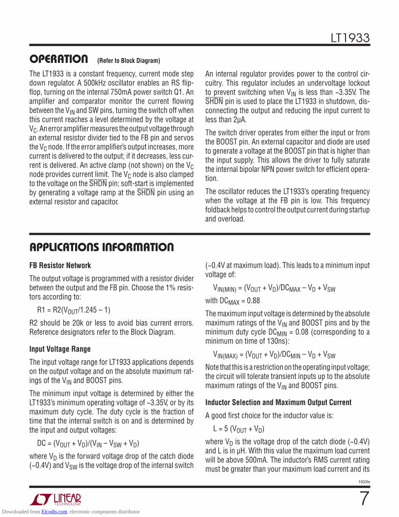
Capacitor C3 and diode D2 are used to generate a boost voltage that is higher than the input voltage. In most cases a 0.1μF capacitor and fast switching diode (such as the 1N4148 or 1N914) will work well. Figure 2 shows two ways to arrange the boost circuit. The BOOST pin must be at least 2.3V above the SW pin for best effi ciency. For outputs of 3V and above, the standard circuit (Figure 2a) is best. For outputs between 2.5V and 3V, use a 0.47μF capacitor and a small Schottky diode (such as the BAT-54). For lower output voltages the boost diode can be tied to the input (Figure 2b). The circuit in Figure 2a is more ef-fi cient because the BOOST pin current comes from a lower voltage source. You must also be sure that the maximum voltage rating of the BOOST pin is not exceeded.
The minimum operating voltage of an LT1933 application is limited by the undervoltage lockout (~3.35V) and by the maximum duty cycle as outlined above. For proper startup, the minimum input voltage is also limited by the boost circuit. If the input voltage is ramped slowly, or the LT1933 is turned on with its SHDN pin when the output is already in regulation, then the boost capacitor may not be fully charged. Because the boost capacitor is charged with the energy stored in the inductor, the circuit will rely on some minimum load current to get the boost circuit running properly. This minimum load will depend on input and output voltages, and on the arrangement of the boost circuit. The minimum load generally goes to zero once the circuit has started. Figure 3 shows a plot of minimum load to start and to run as a function of input voltage. In many
Figure 2. Two Circuits for Generating the Boost Voltage
Figure 3. The Minimum Input Voltage Depends on Output Voltage, Load Current and Boost Circuit
VIN
BOOST
GND
SWVIN
LT1933
(2a)
D2
1933 F02a
VOUT
C3
VBOOST – VSW ≅ VOUTMAX VBOOST ≅ VIN + VOUT
VIN
BOOST
GND
SWVIN
LT1933
(2b)
D2
1933 F02b
VOUT
C3
VBOOST – VSW ≅ VINMAX VBOOST ≅ 2VIN
LOAD CURRENT (mA)
4.5
INP
UT V
OLT
AG
E (
V)
5.0
5.5
6.0
1933 F03a
3.0
3.5
4.0
VOUT = 3.3VTA = 25°CL = 22μH
TO START
TO RUN
1 10 100
LOAD CURRENT (mA)
5
INP
UT V
OLTA
GE (
V)
6
7
8
1933 F03b
4
VOUT = 5VTA = 25°CL = 33μH
TO START
TO RUN
1 10 100
Minimum Input Voltage VOUT = 3.3V Minimum Input Voltage VOUT = 5V
Downloaded from Elcodis.com electronic components distributor
LT1933
121933fe
APPLICATIONS INFORMATIONcases the discharged output capacitor will present a load to the switcher which will allow it to start. The plots show the worst-case situation where VIN is ramping very slowly. For lower start-up voltage, the boost diode can be tied to VIN; however, this restricts the input range to one-half of the absolute maximum rating of the BOOST pin.
At light loads, the inductor current becomes discontinu-ous and the effective duty cycle can be very high. This reduces the minimum input voltage to approximately 300mV above VOUT. At higher load currents, the inductor current is continuous and the duty cycle is limited by the maximum duty cycle of the LT1933, requiring a higher input voltage to maintain regulation.
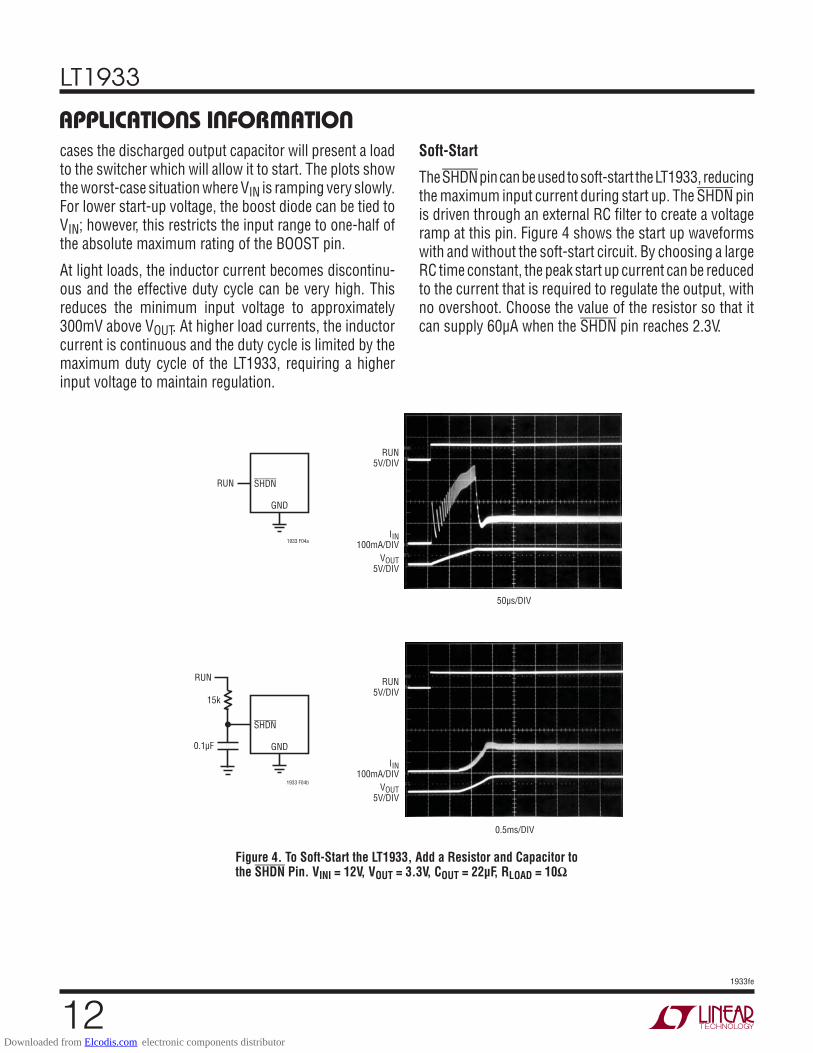
Soft-Start
The SHDN pin can be used to soft-start the LT1933, reducing the maximum input current during start up. The SHDN pin is driven through an external RC fi lter to create a voltage ramp at this pin. Figure 4 shows the start up waveforms with and without the soft-start circuit. By choosing a large RC time constant, the peak start up current can be reduced to the current that is required to regulate the output, with no overshoot. Choose the value of the resistor so that it can supply 60μA when the SHDN pin reaches 2.3V.
Figure 4. To Soft-Start the LT1933, Add a Resistor and Capacitor to the SHDN Pin. VINI = 12V, VOUT = 3.3V, COUT = 22μF, RLOAD = 10Ω
RUN5V/DIV
VOUT5V/DIV
IIN100mA/DIV
RUN SHDN
GND
1933 F04a
50μs/DIV
RUN5V/DIV
VOUT5V/DIV
IIN100mA/DIV
RUN
15k
0.1μF
SHDN
GND
1933 F04b
0.5ms/DIV
Downloaded from Elcodis.com electronic components distributor

LT1933
131933fe
APPLICATIONS INFORMATIONShorted and Reversed Input Protection
If the inductor is chosen so that it won’t saturate exces-sively, an LT1933 buck regulator will tolerate a shorted output. There is another situation to consider in systems where the output will be held high when the input to the LT1933 is absent. This may occur in battery charging ap-plications or in battery backup systems where a battery or some other supply is diode OR-ed with the LT1933’s output. If the VIN pin is allowed to fl oat and the SHDN pin is held high (either by a logic signal or because it is tied to VIN), then the LT1933’s internal circuitry will pull its quiescent current through its SW pin. This is fi ne if your system can tolerate a few mA in this state. If you ground the SHDN pin, the SW pin current will drop to essentially zero. However, if the VIN pin is grounded while the output is held high, then parasitic diodes inside the LT1933 can pull large currents from the output through the SW pin
and the VIN pin. Figure 5 shows a circuit that will run only when the input voltage is present and that protects against a shorted or reversed input.
Hot Plugging Safely
The small size, robustness and low impedance of ceramic capacitors make them an attractive option for the input bypass capacitor of LT1933 circuits. However, these capaci-tors can cause problems if the LT1933 is plugged into a live supply (see Linear Technology Application Note 88 for a complete discussion). The low loss ceramic capacitor combined with stray inductance in series with the power source forms an under damped tank circuit, and the voltage at the VIN pin of the LT1933 can ring to twice the nominal input voltage, possibly exceeding the LT1933’s rating and damaging the part. If the input supply is poorly controlled or the user will be plugging the LT1933 into an energized supply, the input network should be designed to prevent this overshoot.
Figure 5. Diode D4 Prevents a Shorted Input from Discharging a Backup Battery Tied to the Output; It Also Protects the Circuit from a Reversed Input. The LT1933 Rns Only When the Input is Present
VIN BOOST
GND FB
SHDN SW
D4
VIN
LT1933
1933 F05
VOUT
BACKUP
D4: MBR0540
Downloaded from Elcodis.com electronic components distributor

LT1933
141933fe
APPLICATIONS INFORMATION
Figure 6. A Well Chosen Input Network Prevents Input Voltage Overshoot and Ensures Reliable Operation When the LT1933 is Connected to a Live Supply
+
+LT1933
2.2μF
VIN20V/DIV
IIN5A/DIV
20μs/DIV
VIN
CLOSING SWITCHSIMULATES HOT PLUG
IIN
(6a)
(6b)
(6c)
LOWIMPEDANCEENERGIZED24V SUPPLY
STRAYINDUCTANCEDUE TO 6 FEET(2 METERS) OFTWISTED PAIR
+
+LT1933
2.2μF10μF35V
AI.EI.
LT1933
2.2μF0.1μF
1Ω
1933 F06
VIN20V/DIV
IIN5A/DIV
20μs/DIV
VIN20V/DIV
IIN5A/DIV
20μs/DIV
DANGER!
RINGING VIN MAY EXCEEDABSOLUTE MAXIMUMRATING OF THE LT1933
Downloaded from Elcodis.com electronic components distributor

LT1933
151933fe
APPLICATIONS INFORMATIONFigure 6 shows the waveforms that result when an LT1933 circuit is connected to a 24V supply through six feet of 24-gauge twisted pair. The fi rst plot is the response with a 2.2μF ceramic capacitor at the input. The input voltage rings as high as 35V and the input current peaks at 20A. One method of damping the tank circuit is to add another capacitor with a series resistor to the circuit. In Figure 6b an aluminum electrolytic capacitor has been added. This capacitor’s high equivalent series resistance damps the circuit and eliminates the voltage overshoot. The extra capacitor improves low frequency ripple fi ltering and can slightly improve the effi ciency of the circuit, though it is likely to be the largest component in the circuit. An alterna-tive solution is shown in Figure 6c. A 1Ω resistor is added in series with the input to eliminate the voltage overshoot (it also reduces the peak input current). A 0.1μF capacitor improves high frequency fi ltering. This solution is smaller and less expensive than the electrolytic capacitor. For high input voltages its impact on effi ciency is minor, reducing effi ciency less than one half percent for a 5V output at full load operating from 24V.
Frequency Compensation
The LT1933 uses current mode control to regulate the output. This simplifi es loop compensation. In particular, the LT1933 does not require the ESR of the output capaci-tor for stability allowing the use of ceramic capacitors to achieve low output ripple and small circuit size.
Figure 7 shows an equivalent circuit for the LT1933 control loop. The error amp is a transconductance amplifi er with fi nite output impedance. The power section, consisting of the modulator, power switch and inductor, is modeled as a transconductance amplifi er generating an output cur-rent proportional to the voltage at the VC node. Note that the output capacitor integrates this current, and that the capacitor on the VC node (CC) integrates the error ampli-fi er output current, resulting in two poles in the loop. RC provides a zero. With the recommended output capacitor, the loop crossover occurs above the RCCC zero. This simple model works well as long as the value of the inductor is not too high and the loop crossover frequency is much lower than the switching frequency. With a larger ceramic capacitor (very low ESR), crossover may be lower and a phase lead capacitor (CPL) across the feedback divider may improve the phase margin and transient response. Large electrolytic capacitors may have an ESR large enough to create an additional zero, and the phase lead may not be necessary.
If the output capacitor is different than the recommended capacitor, stability should be checked across all operating conditions, including load current, input voltage and tem-perature. The LT1375 data sheet contains a more thorough discussion of loop compensation and describes how to test the stability using a transient load.
Figure 7. Model for Loop Response
–
+
–
+
1.245V
SW
VC
LT1933
GND
1933 F07
R1
OUT
ESR
ERRORAMPLIFIER
CURRENT MODEPOWER STAGE
FB
R2
500k
RC100k
CC80pF
C1
C1
gm =150μmhos
gm
+
CPL
0.7V
1.1mho
Downloaded from Elcodis.com electronic components distributor

LT1933
161933fe
APPLICATIONS INFORMATIONPCB Layout
For proper operation and minimum EMI, care must be taken during printed circuit board layout. Figure 8 shows the recommended component placement with trace, ground plane and via locations. Note that large, switched currents fl ow in the LT1933’s VIN and SW pins, the catch diode (D1) and the input capacitor (C2). The loop formed by these components should be as small as possible and tied to system ground in only one place. These components, along with the inductor and output capacitor, should be placed on the same side of the circuit board, and their connections should be made on that layer. Place a local,
unbroken ground plane below these components, and tie this ground plane to system ground at one location, ideally at the ground terminal of the output capacitor C1. The SW and BOOST nodes should be as small as possible. Finally, keep the FB node small so that the ground pin and ground traces will shield it from the SW and BOOST nodes. Include two vias near the GND pin of the LT1933 to help remove heat from the LT1933 to the ground plane.
Figure 8a shows the layout for the DFN package. Vias near and under the exposed die attach paddle minimize the thermal resistance of the LT1933.
Figure 8. A Good PCB Layout Ensures Proper, Low EMI Operation
GND
VOUT
VIAS
VIN
1933 F08a
D1C1 C2
SHUTDOWN
VIAS
OUTLINE OF LOCAL GROUND PLANE
VIN
VOUT
1933 F08b
SYSTEMGROUND
C2 D1
C1
(8a)DFN Package
(8b)SOT-23 Package
Downloaded from Elcodis.com electronic components distributor

LT1933
171933fe
TYPICAL APPLICATIONS
3.3V Step-Down Converter
12V Step-Down Converter
VIN4.5V TO
36V
OFF ON
C30.1μF
D2
L122μH
R210k
R116.5k
C122μF6.3V
1933 TA02b
C22.2μF
VOUT3.3V/500mA
VIN BOOST
GND FB
SHDN SW
LT1933
D1
VIN14.5V TO
36V
OFF ON
C30.1μF
D3, 6V
D1
L147μH
R210k
R186.6k
C110μF
1933 TA02d
C22.2μF
VOUT12V/450mA
D2
VIN BOOST
GND FB
SHDN SW
LT1933
Downloaded from Elcodis.com electronic components distributor
LT1933
181933fe
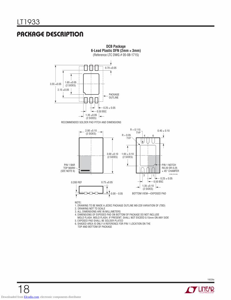
PACKAGE DESCRIPTION
DCB Package6-Lead Plastic DFN (2mm × 3mm)
(Reference LTC DWG # 05-08-1715)
3.00 ±0.10(2 SIDES)
2.00 ±0.10(2 SIDES)
NOTE:1. DRAWING TO BE MADE A JEDEC PACKAGE OUTLINE M0-229 VARIATION OF (TBD)2. DRAWING NOT TO SCALE3. ALL DIMENSIONS ARE IN MILLIMETERS4. DIMENSIONS OF EXPOSED PAD ON BOTTOM OF PACKAGE DO NOT INCLUDE MOLD FLASH. MOLD FLASH, IF PRESENT, SHALL NOT EXCEED 0.15mm ON ANY SIDE5. EXPOSED PAD SHALL BE SOLDER PLATED 6. SHADED AREA IS ONLY A REFERENCE FOR PIN 1 LOCATION ON THE TOP AND BOTTOM OF PACKAGE
0.40 ± 0.10
BOTTOM VIEW—EXPOSED PAD
1.65 ± 0.10(2 SIDES)
0.75 ±0.05
R = 0.115TYP
R = 0.05TYP
1.35 ±0.10(2 SIDES)
13
64
PIN 1 BARTOP MARK
(SEE NOTE 6)
0.200 REF
0.00 – 0.05
(DCB6) DFN 0405
0.25 ± 0.050.50 BSC
PIN 1 NOTCHR0.20 OR 0.25 × 45° CHAMFER
0.25 ± 0.05
1.35 ±0.05(2 SIDES)
RECOMMENDED SOLDER PAD PITCH AND DIMENSIONS
1.65 ±0.05(2 SIDES)
2.15 ±0.05
0.70 ±0.05
3.55 ±0.05
PACKAGEOUTLINE
0.50 BSC
Downloaded from Elcodis.com electronic components distributor
LT1933
191933fe
Information furnished by Linear Technology Corporation is believed to be accurate and reliable. However, no responsibility is assumed for its use. Linear Technology Corporation makes no representa-tion that the interconnection of its circuits as described herein will not infringe on existing patent rights.
PACKAGE DESCRIPTION
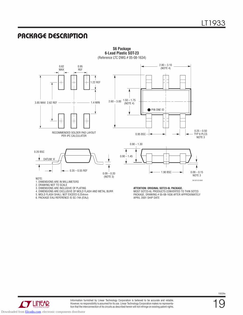
S6 Package6-Lead Plastic SOT-23
(Reference LTC DWG # 05-08-1634)
1.50 – 1.75(NOTE 4)
2.60 – 3.00
0.25 – 0.50TYP 6 PLCS
NOTE 3
DATUM ‘A’
0.09 – 0.20(NOTE 3)
S6 SOT-23 0502
2.80 – 3.10(NOTE 4)
0.95 BSC
1.90 BSC
0.90 – 1.30
0.90 – 1.45
0.09 – 0.15NOTE 3
0.20 BSC
0.35 – 0.55 REF
PIN ONE ID
NOTE:1. DIMENSIONS ARE IN MILLIMETERS2. DRAWING NOT TO SCALE3. DIMENSIONS ARE INCLUSIVE OF PLATING4. DIMENSIONS ARE EXCLUSIVE OF MOLD FLASH AND METAL BURR5. MOLD FLASH SHALL NOT EXCEED 0.254mm6. PACKAGE EIAJ REFERENCE IS SC-74A (EIAJ)
ATTENTION: ORIGINAL SOT23-6L PACKAGE.MOST SOT23-6L PRODUCTS CONVERTED TO THIN SOT23PACKAGE, DRAWING # 05-08-1636 AFTER APPROXIMATELYAPRIL 2001 SHIP DATE
3.85 MAX
0.62MAX
0.95REF
RECOMMENDED SOLDER PAD LAYOUTPER IPC CALCULATOR
1.4 MIN2.62 REF
1.22 REF
Downloaded from Elcodis.com electronic components distributor
LT1933
201933fe
Linear Technology Corporation1630 McCarthy Blvd., Milpitas, CA 95035-7417 (408) 432-1900 ● FAX: (408) 434-0507 ● www.linear.com © LINEAR TECHNOLOGY CORPORATION 2007
LT 0409 REV E • PRINTED IN USA
RELATED PARTS
TYPICAL APPLICATION
PART NUMBER DESCRIPTION COMMENTS
LT1074/LT1074HV 4.4A IOUT, 100kHz, High Effi ciency Step-Down DC/DC Converter
VIN: 7.3V to 45V/64V, VOUT(MIN) = 2.21V, IQ = 8.5mA, ISD = 10μA, DD-5/DD-7, TO220-5/TO220-7 Packages
LT1076/LT1076HV 1.6A IOUT, 100kHz, High Effi ciency Step-Down DC/DC Converter
VIN: 7.3V to 45V/64V, VOUT(MIN) = 2.21V, IQ = 8.5mA, ISD = 10μA, DD-5/DD-7, TO220-5/TO220-7 Packages
LT1676 60V, 440mA IOUT, 100kHz, High Effi ciency Step-Down DC/DC Converter
VIN: 7.4V to 60V, VOUT(MIN) = 1.24V, IQ = 3.2mA, ISD = 2.5μA, S8 Package
LT1765 25V, 2.75mA IOUT, 1.25MHz, High Effi ciency Step-Down DC/DC Converter
VIN: 3V to 25V, VOUT(MIN) = 1.2V, IQ = 1mA, ISD = 15μA, S8, TSSOP16E Packages
LT1766 60V, 1.2A IOUT, 200kHz, High Effi ciency Step-Down DC/DC Converter
VIN: 5.5V to 60V, VOUT(MIN) = 1.2V, IQ = 2.5mA, ISD = 25μA, S8, TSSOP16/TSSOP16E Packages
LT1767 25V, 1.2A IOUT, 1.25MHz, High Effi ciency Step-Down DC/DC Converter
VIN: 3V to 25V, VOUT(MIN) = 1.2V, IQ = 1mA, ISD = 6μA, S8, MS8/MS8E Packages
LT1776 40V, 550mA IOUT, 200kHz, High Effi ciency Step-Down DC/DC Converter
VIN: 7.4V to 40V, VOUT(MIN) = 1.24V, IQ = 3.2mA, ISD = 30μA, S8, N8, S8 Packages
LT1940 25V, Dual 1.4A IOUT, 1.1MHz, High Effi ciency Step-Down DC/DC Converter
VIN: 3.6V to 25V, VOUT(MIN) = 1.25V, IQ = 3.8mA, ISD < 30μA, TSSOP16E Package
LT1956 60V, Dual 1.2A IOUT, 500kHz, High Effi ciency Step-Down DC/DC Converter
VIN: 5.5V to 60V, VOUT(MIN) = 1.2V, IQ = 2.5mA, ISD = 25μA, TSSOP16/TSSOP16E Packages
LT1976 60V, Dual 1.2A IOUT, 200kHz, High Effi ciency Step-Down DC/DC Converter with Burst Mode®
VIN: 3.3V to 60V, VOUT(MIN) = 1.2V, IQ = 100μA, ISD < 1μA, TSSOP16E Package
LT3010 80V, 50mA, Low Noise Linear Regulator VIN: 1.5V to 80V, VOUT(MIN) = 1.28V, IQ = 30μA, ISD < 1μA, MS8E Package
LT3407 Dual 600mA IOUT, 1.5MHz, Synchronous Step-Down DC/DC Converter
VIN: 2.5V to 5.5V, VOUT(MIN) = 0.6V, IQ = 40μA, ISD < 1μA, MS10E Package
LT3412 2.5A IOUT, 4MHz, Synchronous Step-Down DC/DC Converter
VIN: 2.5V to 5.5V, VOUT(MIN) = 0.8V, IQ = 60μA, ISD < 1μA, TSSOP16E Package
LTC3414 4A IOUT, 4MHz, Synchronous Step-Down DC/DC Converter VIN: 2.3V to 5.5V, VOUT(MIN) = 0.8V, IQ = 64μA, ISD < 1μA, TSSOP20E Package
LT3430/LT3431 60V, 2.75A IOUT, 200kHz/500kHz, Synchronous Step-Down DC/DC Converter
VIN: 5.5V to 60V, VOUT(MIN) = 1.2V, IQ = 2.5mA, ISD = 30μA, TSSOP16E Package
Burst Mode is a registered trademark of Linear Technology Corporation.
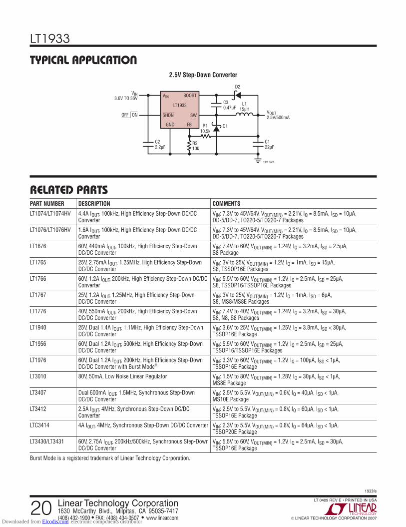
2.5V Step-Down Converter
VIN3.6V TO 36V
OFF ON
C30.47μF
D2
L115μH
R210k
R110.5k
C122μF
1933 TA03
C22.2μF
VOUT2.5V/500mA
VIN BOOST
GND FB
SHDN SW
LT1933
D1
Downloaded from Elcodis.com electronic components distributor