LT1228 - 100MHz Current Feedback Amplifier with …cds.linear.com/docs/en/datasheet/1228fd.pdfLT1228...
22
LT1228 1 1228fd TYPICAL APPLICATION FEATURES DESCRIPTION 100MHz Current Feedback Amplifier with DC Gain Control The LT ® 1228 makes it easy to electronically control the gain of signals from DC to video frequencies. The LT1228 implements gain control with a transconductance ampli- fier (voltage to current) whose gain is proportional to an externally controlled current. A resistor is typically used to convert the output current to a voltage, which is then amplified with a current feedback amplifier. The LT1228 combines both amplifiers into an 8-pin package, and oper- ates on any supply voltage from 4V (±2V) to 30V (±15V). A complete differential input, gain controlled amplifier can be implemented with the LT1228 and just a few resistors. The LT1228 transconductance amplifier has a high imped- ance differential input and a current source output with wide output voltage compliance. The transconductance, g m , is set by the current that flows into Pin 5, I SET . The small signal g m is equal to ten times the value of I SET and this relationship holds over several decades of set current. The voltage at Pin 5 is two diode drops above the negative supply, Pin 4. The LT1228 current feedback amplifier has very high input impedance and therefore it is an excellent buffer for the out- put of the transconductance amplifier. The current feedback amplifier maintains its wide bandwidth over a wide range of voltage gains making it easy to interface the transconduc- tance amplifier output to other circuitry. The current feed- back amplifier is designed to drive low impedance loads, such as cables, with excellent linearity at high frequencies. APPLICATIONS n Very Fast Transconductance Amplifier Bandwidth: 75MHz g m = 10 × I SET Low THD: 0.2% at 30mV RMS Input Wide I SET Range: 1µA to 1mA n Very Fast Current Feedback Amplifier Bandwidth: 100MHz Slew Rate: 1000V/µs Output Drive Current: 30mA Differential Gain: 0.04% Differential Phase: 0.1° High Input Impedance: 25MΩ, 6pF n Wide Supply Range: ±2V to ±15V n Inputs Common Mode to Within 1.5V of Supplies n Outputs Swing Within 0.8V of Supplies n Supply Current: 7mA n Available in 8-Lead PDIP and SO Packages n Video DC Restore (Clamp) Circuits n Video Differential Input Amplifiers n Video Keyer/Fader Amplifiers n AGC Amplifiers n Tunable Filters n Oscillators L, LT, LTC, LTM, Linear Technology and the Linear logo are registered trademarks of Linear Technology Corporation. All other trademarks are the property of their respective owners. LT1228 • TA01 – + – + + + R3A 10k R2A 10k R3 100Ω R2 100Ω 4.7μF R4 1.24k R6 6.19k R5 10k I SET R1 270Ω R G 10Ω R F 470Ω 4.7μF 15V g m CFA V OUT 1 8 6 3 2 7 5 4 –15V + – V IN HIGH INPUT RESISTANCE EVEN WHEN POWER IS OFF –18dB < GAIN < 2dB V IN ≤ 3V RMS FREQUENCY (Hz) 100k –24 GAIN (dB) –15 –3 3 6 1M 10M 100M LT1228 • TA02 0 –6 –9 –12 –18 –21 I SET = 100μA V S = ±15V R L = 100Ω I SET = 1mA I SET = 300μA Differential Input Variable Gain Amp Frequency Response
Transcript of LT1228 - 100MHz Current Feedback Amplifier with …cds.linear.com/docs/en/datasheet/1228fd.pdfLT1228...

LT1228
11228fd
TYPICAL APPLICATION
FEATURES DESCRIPTION
100MHz Current Feedback Amplifier with DC Gain Control
The LT®1228 makes it easy to electronically control the gain of signals from DC to video frequencies. The LT1228 implements gain control with a transconductance ampli-fier (voltage to current) whose gain is proportional to an externally controlled current. A resistor is typically used to convert the output current to a voltage, which is then amplified with a current feedback amplifier. The LT1228 combines both amplifiers into an 8-pin package, and oper-ates on any supply voltage from 4V (±2V) to 30V (±15V). A complete differential input, gain controlled amplifier can be implemented with the LT1228 and just a few resistors.
The LT1228 transconductance amplifier has a high imped-ance differential input and a current source output with wide output voltage compliance. The transconductance, gm, is set by the current that flows into Pin 5, ISET. The small signal gm is equal to ten times the value of ISET and this relationship holds over several decades of set current. The voltage at Pin 5 is two diode drops above the negative supply, Pin 4.
The LT1228 current feedback amplifier has very high input impedance and therefore it is an excellent buffer for the out-put of the transconductance amplifier. The current feedback amplifier maintains its wide bandwidth over a wide range of voltage gains making it easy to interface the transconduc-tance amplifier output to other circuitry. The current feed-back amplifier is designed to drive low impedance loads, such as cables, with excellent linearity at high frequencies.
APPLICATIONS
n Very Fast Transconductance Amplifier Bandwidth: 75MHz gm = 10 × ISET Low THD: 0.2% at 30mVRMS Input Wide ISET Range: 1µA to 1mAn Very Fast Current Feedback Amplifier Bandwidth: 100MHz Slew Rate: 1000V/µs Output Drive Current: 30mA Differential Gain: 0.04% Differential Phase: 0.1° High Input Impedance: 25MΩ, 6pFn Wide Supply Range: ±2V to ±15Vn Inputs Common Mode to Within 1.5V of Suppliesn Outputs Swing Within 0.8V of Suppliesn Supply Current: 7mAn Available in 8-Lead PDIP and SO Packages
n Video DC Restore (Clamp) Circuitsn Video Differential Input Amplifiersn Video Keyer/Fader Amplifiersn AGC Amplifiersn Tunable Filtersn OscillatorsL, LT, LTC, LTM, Linear Technology and the Linear logo are registered trademarks of Linear Technology Corporation. All other trademarks are the property of their respective owners.
LT1228 • TA01
–
+–
+
+
+
R3A10k
R2A10k
R3100Ω
R2100Ω
4.7µFR41.24k
R66.19k
R510k
ISET
R1270Ω
RG10Ω
RF470Ω
4.7µF15V
gm
CFA VOUT
1
8
6
3
2
7
54
–15V
+
–VIN
HIGH INPUT RESISTANCEEVEN WHEN POWER IS OFF–18dB < GAIN < 2dBVIN ≤ 3VRMS
FREQUENCY (Hz)
100k–24
GAIN
(dB)
–15
–3
3
6
1M 10M 100M
LT1228 • TA02
0
–6
–9
–12
–18
–21ISET = 100µA
VS = ±15VRL = 100Ω
ISET = 1mA
ISET = 300µA
Differential Input Variable Gain AmpFrequency Response

LT1228
21228fd
PIN CONFIGURATIONABSOLUTE MAXIMUM RATINGS(Note 1)
ORDER INFORMATIONLEAD FREE FINISH TAPE AND REEL PART MARKING PACKAGE DESCRIPTION TEMPERATURE RANGE
LT1228CN8#PBF LT1228CN8#TRPBF LT1228CN8 8-Lead Plastic DIP 0°C to 70°C
LT1228IN8#PBF LT1228IN8#TRPBF LT1228IN8 8-Lead Plastic DIP –40°C to 85°C
LT1228CS8#PBF LT1228CS8#TRPBF 1228 8-Lead Plastic SO 0°C to 70°C
LT1228IS8#PBF LT1228IS8#TRPBF 1228I 8-Lead Plastic SO –40°C to 85°C
OBSOLETE PACKAGE
LT1228MJ8 LT1228MJ8#TRPBF LT1228MJ8 8-Lead CERDIP –55°C to 125°C
LT1228CJ8 LT1228CJ8#TRPBF LT1228CJ8 8-Lead CERDIP 0°C to 70°C
Consult LTC Marketing for parts specified with wider operating temperature ranges. Consult LTC Marketing for information on nonstandard lead based finish parts.For more information on lead free part marking, go to: http://www.linear.com/leadfree/ For more information on tape and reel specifications, go to: http://www.linear.com/tapeandreel/
ELECTRICAL CHARACTERISTICS The l denotes the specifications which apply over the full operating temperature range, otherwise specifications are at TA = 25°C. Current Feedback Amplifier, Pins 1, 6, 8. ±5V ≤ VS ≤ ±15V, ISET = 0µA, VCM = 0V unless otherwise noted.
8
7
6
54
3
2
1IOUT
–IN
+IN
V– ISET
VOUT
V+
GAIN
TOP VIEW
N8 PACKAGE8-LEAD PDIP
S8 PACKAGE8-LEAD PLASTIC SO
+ –gm
TJMAX = 150°C, θJA = 100°C/W (N)TJMAX = 150°C, θJA = 150°C/W (N)
J8 PACKAGE8-LEAD CERDIP
TJMAX = 175°C, θJA = 100°C/W (J)
OBSOLETE PACKAGE
SYMBOL PARAMETER CONDITIONS MIN TYP MAX UNITS
VOS Input Offset Voltage TA = 25°C
l
±3 ±10 ±15
mV mV
Input Offset Voltage Drift l 10 µV/°C
IIN+ Noninverting Input Current TA = 25°C
l
±0.3 ±3 ±10
µA µA
IIN– Inverting Input Current TA = 25°C
l
±10 ±65 ±100
µA µA
en Input Noise Voltage Density f = 1kHz, RF = 1k, RG = 10Ω, RS = 0Ω 6 nV/√Hz
in Input Noise Current Density f = 1kHz, RF = 1k, RG = 10Ω, RS = 10k 1.4 pV/√Hz
Supply Voltage ....................................................... ±18VInput Current, Pins 1, 2, 3, 5, 8 (Note 8) ..............±15mAOutput Short Circuit Duration (Note 2) .........ContinuousOperating Temperature Range LT1228C ...................................................0°C to 70°C LT1228I ................................................–40°C to 85°C LT1228M (OBSOLETE) ...................... –55°C to 125°CStorage Temperature Range ..................–65°C to 150°CJunction Temperature Plastic Package ................................................. 150°C Ceramic Package (OBSOLETE) ......................... 175°CLead Temperature (Soldering, 10 sec) ...................300°C

LT1228
31228fd
ELECTRICAL CHARACTERISTICS The l denotes the specifications which apply over the full operating temperature range, otherwise specifications are at TA = 25°C. Current Feedback Amplifier, Pins 1, 6, 8. ±5V ≤ VS ≤ ±15V, ISET = 0µA, VCM = 0V unless otherwise noted.
SYMBOL PARAMETER CONDITIONS MIN TYP MAX UNITS
RIN Input Resistance VIN = ±13V, VS = ±15V VIN = ±3V, VS = ±5V
l
l
2 2
25 25
MΩ MΩ
CIN Input Capacitance (Note 3) VS = ±5V 6 pF
Input Voltage Range VS = ±15V, TA = 25°C
l
±13 ±12
±13.5 V V
VS = ±5V, TA = 25°C
l
±3 ±2
±3.5 V V
CMRR Common Mode Rejection Ratio VS = ±15V, VCM = ±13V, TA = 25°C VS = ±15V, VCM = ±12V VS = ±5V, VCM = ±3V, TA = 25°C VS = ±5V, VCM = ±2V
l
l
55 55 55 55
69
69
dB dB dB dB
Inverting Input Current Common Mode Rejection
VS = ±15V, VCM = ±13V, TA = 25°C VS = ±15V, VCM = ±12V VS = ±5V, VCM = ±3V, TA = 25°C VS = ±5V, VCM = ±2V
l
l
2.5
2.5
10 10 10 10
µA/V µA/V µA/V µA/V
PSRR Power Supply Rejection Ratio VS = ±2V to ±15V, TA = 25°C VS = ±3V to ±15V
l
60 60
80 dB dB
Noninverting Input Current Power Supply Rejection
VS = ±2V to ±15V, TA = 25°C VS = ±3V to ±15V
l
10 50 50
nA/V nA/V
Inverting Input Current Power Supply Rejection
VS = ±2V to ±15V, TA = 25°C VS = ±3V to ±15V
l
0.1 5 5
µA/V µA/V
AV Large-Signal Voltage Gain VS = ±15V, VOUT = ±10V, RLOAD = 1k VS = ±5V, VOUT = ±2V, RLOAD = 150Ω
l
l
55 55
65 65
dB dB
ROL Transresistance, ∆VOUT/∆IIN– VS = ±15V, VOUT = ±10V, RLOAD = 1k VS = ±5V, VOUT = ±2V, RLOAD = 150Ω
l
l
100 100
200 200
kΩ kΩ
VOUT Maximum Output Voltage Swing VS = ±15V, RLOAD = 400Ω, TA = 25°C
l
±12 ±10
±13.5 V V
VS = ±5V, RLOAD = 150Ω, TA = 25°C
l
±3 ±2.5
±3.7 V V
IOUT Maximum Output Current RLOAD = 0Ω, TA = 25°C
l
30 25
65 125 125
mA mA
IS Supply Current VOUT = 0V, ISET = 0V l 6 11 mA
SR Slew Rate (Notes 4 and 6) TA = 25°C 300 500 V/µs
SR Slew Rate VS = ±15V, RF = 750Ω, RG = 750Ω, RL = 400Ω 3500 V/µs
tr Rise Time (Notes 5 and 6) TA = 25°C 10 20 ns
BW Small-Signal Bandwidth VS = ±15V, RF = 750Ω, RG = 750Ω, RL = 100Ω 100 MHz
tr Small-Signal Rise Time VS = ±15V, RF = 750Ω, RG = 750Ω, RL = 100Ω 3.5 ns
Propagation Delay VS = ±15V, RF = 750Ω, RG = 750Ω, RL = 100Ω 3.5 ns
Small-Signal Overshoot VS = ±15V, RF = 750Ω, RG = 750Ω, RL = 100Ω 15 %
tS Settling Time 0.1%, VOUT = 10V, RF =1k, RG = 1k, RL =1k 45 ns
Differential Gain (Note 7) VS = ±15V, RF = 750Ω, RG = 750Ω, RL = 1k 0.01 %
Differential Phase (Note 7) VS = ±15V, RF = 750Ω, RG = 750Ω, RL = 1k 0.01 DEG
Differential Gain (Note 7) VS = ±15V, RF = 750Ω, RG = 750Ω, RL = 150Ω 0.04 %
Differential Phase (Note 7) VS = ±15V, RF = 750Ω, RG = 750Ω, RL = 150Ω 0.1 DEG
LT1228
41228fd
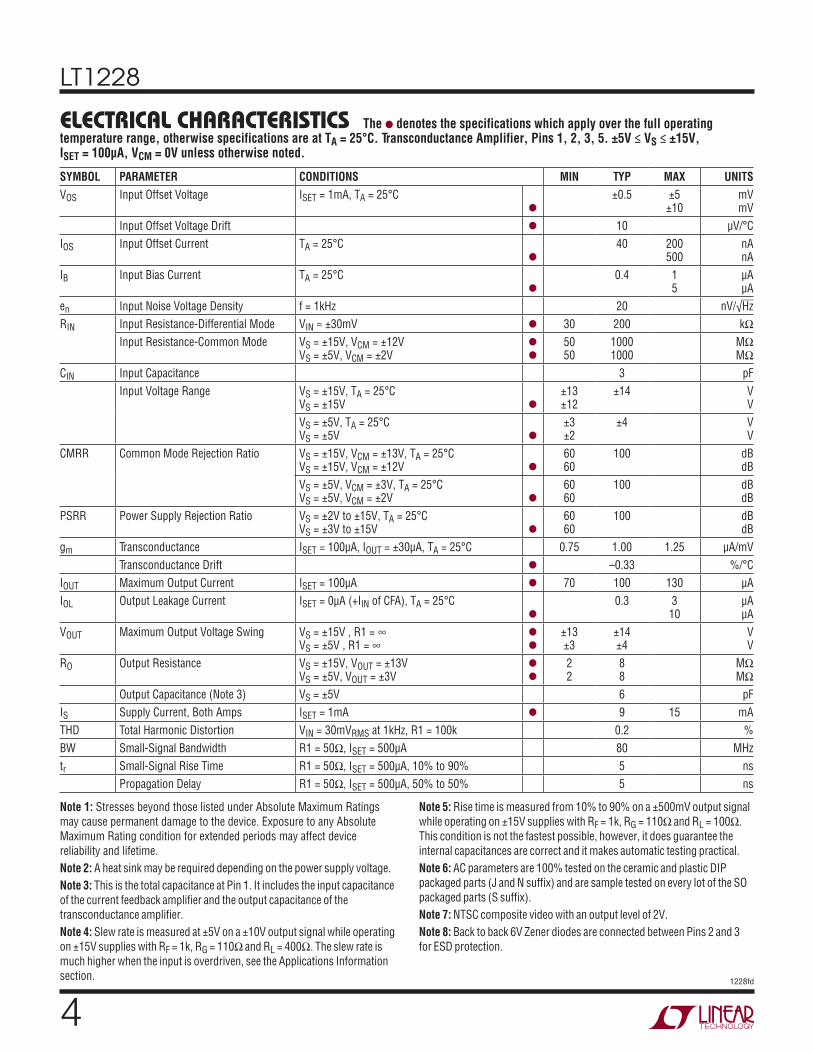
ELECTRICAL CHARACTERISTICS The l denotes the specifications which apply over the full operating temperature range, otherwise specifications are at TA = 25°C. Transconductance Amplifier, Pins 1, 2, 3, 5. ±5V ≤ VS ≤ ±15V, ISET = 100µA, VCM = 0V unless otherwise noted.
SYMBOL PARAMETER CONDITIONS MIN TYP MAX UNITSVOS Input Offset Voltage ISET = 1mA, TA = 25°C
l
±0.5 ±5 ±10
mV mV
Input Offset Voltage Drift l 10 µV/°CIOS Input Offset Current TA = 25°C
l
40 200 500
nA nA
IB Input Bias Current TA = 25°C
l
0.4 1 5
µA µA
en Input Noise Voltage Density f = 1kHz 20 nV/√HzRIN Input Resistance-Differential Mode VIN ≈ ±30mV l 30 200 kΩ
Input Resistance-Common Mode VS = ±15V, VCM = ±12V VS = ±5V, VCM = ±2V
l
l
50 50
1000 1000
MΩ MΩ
CIN Input Capacitance 3 pFInput Voltage Range VS = ±15V, TA = 25°C
VS = ±15V
l
±13 ±12
±14 V V
VS = ±5V, TA = 25°C VS = ±5V
l
±3 ±2
±4 V V
CMRR Common Mode Rejection Ratio VS = ±15V, VCM = ±13V, TA = 25°C VS = ±15V, VCM = ±12V
l
60 60
100 dB dB
VS = ±5V, VCM = ±3V, TA = 25°C VS = ±5V, VCM = ±2V
l
60 60
100 dB dB
PSRR Power Supply Rejection Ratio VS = ±2V to ±15V, TA = 25°C VS = ±3V to ±15V
l
60 60
100 dB dB
gm Transconductance ISET = 100µA, IOUT = ±30µA, TA = 25°C 0.75 1.00 1.25 µA/mVTransconductance Drift l –0.33 %/°C
IOUT Maximum Output Current ISET = 100µA l 70 100 130 µAIOL Output Leakage Current ISET = 0µA (+IIN of CFA), TA = 25°C
l
0.3 3 10
µA µA
VOUT Maximum Output Voltage Swing VS = ±15V , R1 = ∞ VS = ±5V , R1 = ∞
l
l
±13 ±3
±14 ±4
V V
RO Output Resistance VS = ±15V, VOUT = ±13V VS = ±5V, VOUT = ±3V
l
l
2 2
8 8
MΩ MΩ
Output Capacitance (Note 3) VS = ±5V 6 pFIS Supply Current, Both Amps ISET = 1mA l 9 15 mATHD Total Harmonic Distortion VIN = 30mVRMS at 1kHz, R1 = 100k 0.2 %BW Small-Signal Bandwidth R1 = 50Ω, ISET = 500µA 80 MHztr Small-Signal Rise Time R1 = 50Ω, ISET = 500µA, 10% to 90% 5 ns
Propagation Delay R1 = 50Ω, ISET = 500µA, 50% to 50% 5 ns
Note 1: Stresses beyond those listed under Absolute Maximum Ratings may cause permanent damage to the device. Exposure to any Absolute Maximum Rating condition for extended periods may affect device reliability and lifetime.Note 2: A heat sink may be required depending on the power supply voltage.Note 3: This is the total capacitance at Pin 1. It includes the input capacitance of the current feedback amplifier and the output capacitance of the transconductance amplifier.Note 4: Slew rate is measured at ±5V on a ±10V output signal while operating on ±15V supplies with RF = 1k, RG = 110Ω and RL = 400Ω. The slew rate is much higher when the input is overdriven, see the Applications Information section.
Note 5: Rise time is measured from 10% to 90% on a ±500mV output signal while operating on ±15V supplies with RF = 1k, RG = 110Ω and RL = 100Ω. This condition is not the fastest possible, however, it does guarantee the internal capacitances are correct and it makes automatic testing practical.Note 6: AC parameters are 100% tested on the ceramic and plastic DIP packaged parts (J and N suffix) and are sample tested on every lot of the SO packaged parts (S suffix).Note 7: NTSC composite video with an output level of 2V.Note 8: Back to back 6V Zener diodes are connected between Pins 2 and 3 for ESD protection.

LT1228
51228fd
TYPICAL PERFORMANCE CHARACTERISTICS
Total Harmonic Distortion vs Input Voltage
Spot Output Noise Current vs Frequency
Input Common Mode Limit vs Temperature
Small-Signal Control Path Bandwidth vs Set Current
Small-Signal Control Path Gain vs Input Voltage
Output Saturation Voltage vs Temperature
Small-Signal Bandwidth vs Set Current
Small-Signal Transconductance and Set Current vs Bias Voltage
Small-Signal Transconductance vs DC Input Voltage
Transconductance Amplifier, Pins 1, 2, 3, 5
SET CURRENT (µA)
100.1
–3dB
BAN
DWID
TH (M
Hz)
1
10
100
100 1000
LT1228 • TPC01
R1 = 100k
R1 = 10k
R1 = 1k
R1 = 100ΩVS = ±15V
BIAS VOLTAGE, PIN 5 TO 4, (V)
0.01TRAN
SCON
DUCT
ANCE
(µA/
mV)
0.1
1
10
100
0.9 1.2 1.3 1.5
LT1228 • TPC02
0.0011.0 1.1 1.4
VS = ±2V TO ±15VTA = 25°C
1.0
10
100
1000
10000
0.1
SET CURRENT (µA)
INPUT VOLTAGE (mVDC)
–2000
TRAN
SCON
DUCT
ANCE
(µA/
mV)
0.2
0.4
1.4
2.0
–150 –100 –50 200
LT1228 • TPC03
0 100 150
1.8
1.6
1.2
0.6
0.8
–55°C
VS = ±2V TO ±15VISET = 100µA
50
1.025°C
125°C
INPUT VOLTAGE (mVP–P)
10.01
OUTP
UT D
ISTO
RTIO
N (%
)
0.1
1
10
10 1000
LT1228 • TPC04
ISET = 100µA
VS = ±15V
ISET = 1mA
100
FREQUENCY (Hz)
1010
SPOT
NOI
SE (p
A/√H
z)
100
1000
1k 100k
LT1228 • TPC05
VS = ±2V TO ±15VTA = 25°C
100 10k
ISET = 1mA
ISET = 100µA
TEMPERATURE (°C)
–50V–
COM
MON
MOD
E RA
NGE
(V)
0.5
1.0
–1.5
V+
–25 0 25 125
LT1228 • TPC06
50 75 100
–0.5
–1.0
–2.0
1.5
2.0
V– = –2V TO –15V
V+ = 2V TO 15V
SET CURRENT (µA)
101
–3dB
BAN
DWID
TH (M
Hz)
10
100
100 1000
LT1228 • TPC07
VS = ±2V TO ±15VVIN = 200mV(PIN 2 TO 3)
∆IOUT∆ISET
INPUT VOLTAGE, PIN 2 TO 3, (mVDC)
00
CONT
ROL
PATH
GAI
N (µ
A/µA
)
1.0
120 200
LT1228 • TPC08
∆IOUT∆ISET
40 80 160
0.2
0.4
0.6
0.8
0.9
0.7
0.5
0.3
0.1
TEMPERATURE (°C)
–50V–
OUTP
UT S
ATUR
ATIO
N VO
LTAG
E (V
)
+0.5
+1.0
–1.0
V+
–25 0 25 125
LT1228 • TPC09
50 75 100
–0.5
±2V ≤ VS ≤ ±15VR1 = ∞

LT1228
61228fd
TYPICAL PERFORMANCE CHARACTERISTICS
Voltage Gain and Phase vs Frequency, Gain = 20dB
–3dB Bandwidth vs Supply Voltage, Gain = 10, RL = 100Ω
–3dB Bandwidth vs Supply Voltage, Gain = 10, RL = 1k
Voltage Gain and Phase vs Frequency, Gain = 40dB
–3dB Bandwidth vs Supply Voltage, Gain = 100, RL = 100Ω
–3dB Bandwidth vs Supply Voltage, Gain = 100, RL = 1k
Voltage Gain and Phase vs Frequency, Gain = 6dB
–3dB Bandwidth vs Supply Voltage, Gain = 2, RL = 100Ω
–3dB Bandwidth vs Supply Voltage, Gain = 2, RL = 1k
Transconductance Amplifier, Pins 1, 6, 8
FREQUENCY (MHz)
0
VOLT
AGE
GAIN
(dB)
2
4
6
8
0.1 10 100
LT1228 • TPC10
–21
7
5
3
1
–1
PHASE SHIFT (DEG)
180
90
0
45
135
225
PHASE
GAIN
VS = ±15VRL = 100ΩRF = 750Ω
SUPPLY VOLTAGE (±V)
2
–3dB
BAN
DWID
TH (M
Hz)
40
100
120
12 16
LT1228 • TPC11
40 6 8 10 14 180
20
60
140
160
180
RF = 500Ω
80
PEAKING ≤ 0.5dBPEAKING ≤ 5dB
RF = 750Ω
RF = 1k
RF = 2k
SUPPLY VOLTAGE (±V)
2
–3dB
BAN
DWID
TH (M
Hz)
40
100
120
12 16
LT1228 • TPC12
40 6 8 10 14 180
20
60
140
160
180
80PEAKING ≤ 0.5dBPEAKING ≤ 5dB
RF = 750Ω
RF = 1k RF = 2k
RF = 500Ω
FREQUENCY (MHz)
14
VOLT
AGE
GAIN
(dB)
16
18
20
22
0.1 10 100
LT1228 • TPC13
121
21
19
17
15
13
PHASE SHIFT (DEG)
180
90
0
45
135
225
PHASE
GAIN
VS = ±15VRL = 100ΩRF = 750Ω
SUPPLY VOLTAGE (±V)
2
–3dB
BAN
DWID
TH (M
Hz)
40
100
120
12 16
LT1228 • TPC14
40 6 8 10 14 180
20
60
140
160
180
RF = 500Ω80
PEAKING ≤ 0.5dBPEAKING ≤ 5dB
RF = 750Ω
RF = 1k
RF = 2k
RF = 250Ω
SUPPLY VOLTAGE (±V)
2
–3dB
BAN
DWID
TH (M
Hz)
40
100
120
12 16
LT1228 • TPC15
40 6 8 10 14 180
20
60
140
160
180
RF = 500Ω
80
PEAKING ≤ 0.5dBPEAKING ≤ 5dB
RF = 750Ω
RF = 1k
RF = 2k
RF = 250Ω
FREQUENCY (MHz)
34
VOLT
AGE
GAIN
(dB)
36
38
40
42
0.1 10 100
LT1228 • TPC16
321
41
39
37
35
33
PHASE SHIFT (DEG)
180
90
0
45
135
225
PHASE
GAIN
VS = ±15VRL = 100ΩRF = 750Ω
SUPPLY VOLTAGE (±V)
2
–3dB
BAN
DWID
TH (M
Hz)
4
10
12
12 16
LT1228 • TPC17
40 6 8 10 14 180
2
6
14
16
18
RF = 500Ω
8RF = 1k
RF = 2k
SUPPLY VOLTAGE (±V)
2
–3dB
BAN
DWID
TH (M
Hz)
4
10
12
12 16
LT1228 • TPC18
40 6 8 10 14 180
2
6
14
16
18
RF = 500Ω
8
RF = 1k
RF = 2k

LT1228
71228fd
TYPICAL PERFORMANCE CHARACTERISTICS
Input Common Mode Limit vs Temperature
Output Saturation Voltage vs Temperature
Output Short-Circuit Current vs Temperature
Spot Noise Voltage and Current vs Frequency
Power Supply Rejection vs Frequency Output Impedance vs Frequency
Maximum Capacitive Load vs Feedback Resistor
Total Harmonic Distortion vs Frequency
2nd and 3rd Harmonic Distortion vs Frequency
Transconductance Amplifier, Pins 1, 6, 8
FEEDBACK RESISTOR (kΩ)
10CAPA
CITI
VE L
OAD
(pF)
100
1k
10k
0 2 3
LT1228 • TPC19
11
VS = ±5V
VS = ±15V
RL = 1kPEAKING ≤ 5dBGAIN = 2
FREQUENCY (Hz)
TOTA
L HA
RMON
IC D
ISTO
RTIO
N (%
)
0.01
0.10
10 1k 10k 100k
LT1228 • TPC20
0.001100
VS = ±15VRL = 400ΩRF = RG = 750Ω
VO = 7VRMS
VO = 1VRMS
FREQUENCY (MHz)
1–70
DIST
ORTI
ON (d
Bc)
–60
–50
–40
–30
–20
10 100
LT1228 • TPC21
VS = ±15VVO = 2VP–PRL = 100ΩRF = 750ΩAV = 10dB 2nd
3rd
TEMPERATURE (°C)
COM
MON
MOD
E RA
NGE
(V)
2.0
V+
–50 25 75 125
LT1228 • TPC22
V–
0
1.0
–1.0
–2.0
–0.5
–1.5
1.5
0.5
–25 50 100
V+ = 2V TO 15V
V– = –2V TO –15V
TEMPERATURE (°C)
OUTP
UT S
ATUR
ATIO
N VO
LTAG
E (V
)
V+
–50 25 75 125
LT1228 • TPC23
V–
0
1.0
–1.0
–0.5
0.5
–25 50 100
RL = ∞±2V ≤ VS ≤ 15V
TEMPERATURE (°C)
–25
OUTP
UT S
HORT
-CIR
CUIT
CUR
RENT
(mA)
40
60
100 150
LT1228 • TPC24
0–50 25 50 75 125 17530
70
50
FREQUENCY (Hz)
SPOT
NOI
SE (n
V/√H
z OR
pA/
√Hz)
10
100
10 1k 10k 100k
LT1228 • TPC25
1100
en
+in
–in
FREQUENCY (Hz)
POW
ER S
UPPL
Y RE
JECT
ION
(dB)
40
80
10k 1M 10M 100M
LT1228 • TPC26
0100k
VS = ±15VRL = 100ΩRF = RG = 750Ω
NEGATIVE20
60POSITIVE
FREQUENCY (Hz)
OUTP
UT IM
PEDA
NCE
(Ω)
0.1
100
10k 1M 10M 100M
LT1228 • TPC27
0.001100k
0.01
10
VS = ±15V
1.0RF = RG = 2k
RF = RG = 750Ω

LT1228
81228fd
TYPICAL PERFORMANCE CHARACTERISTICS
SIMPLIFIED SCHEMATIC
Current Feedback Amplifier, Pins 1, 6, 8
Setting Time to 10mV vs Output Step
Setting Time to 1mV vs Output Step Supply Current vs Supply Voltage
SETTLING TIME (ns)
OUTP
UT S
TEP
(V)
60
LT1228 • TPC28
200 40 80 100–10
10
0
–8
–6
–4
–2
2
4
6
8 NONINVERTING
INVERTING
VS = ±15VRF = RG = 1k
INVERTING
NONINVERTING
SETTLING TIME (µs)
OUTP
UT S
TEP
(V)
12
LT1228 • TPC29
40 8 16 20–10
10
0
–8
–6
–4
–2
2
4
6
8 NONINVERTING
INVERTING
VS = ±15VRF = RG = 1k
NONINVERTING
INVERTING
SUPPLY VOLTAGE (±V)
SUPP
LY C
URRE
NT (m
A)
12
LT1228 • TPC30
40 8 160
10
5
1
2
3
4
6
7
8
9
2 6 10 14 18
–55°C
25°C
125°C
175°C
LT1228 • TA03
IOUT GAIN VOUT
V+
V–
–IN+IN
ISET
BIAS
123
5
6
4
7
8
LT1228
91228fd
APPLICATIONS INFORMATIONThe LT1228 contains two amplifiers, a transconductance amplifier (voltage-to-current) and a current feedback ampli-fier (voltage-to-voltage). The gain of the transconductance amplifier is proportional to the current that is externally programmed into Pin 5. Both amplifiers are designed to operate on almost any available supply voltage from 4V (±2V) to 30V (±15V). The output of the transconductance amplifier is connected to the noninverting input of the current feedback amplifier so that both fit into an eight pin package.
TRANSCONDUCTANCE AMPLIFIER
The LT1228 transconductance amplifier has a high imped-ance differential input (Pins 2 and 3) and a current source output (Pin 1) with wide output voltage compliance. The voltage to current gain or transconductance (gm) is set by the current that flows into Pin 5, ISET. The voltage at Pin 5 is two forward biased diode drops above the nega-tive supply, Pin 4. Therefore the voltage at Pin 5 (with respect to V–) is about 1.2V and changes with the log of the set current (120mV/decade), see the characteristic curves. The temperature coefficient of this voltage is about –4mV/°C (–3300ppm/°C) and the temperature coefficient of the logging characteristic is 3300ppm/°C. It is important that the current into Pin 5 be limited to less than 15mA. THE LT1228 WILL BE DESTROYED IF PIN 5 IS SHORTED TO GROUND OR TO THE POSITIVE SUPPLY. A limiting resistor (2k or so) should be used to prevent more than 15mA from flowing into Pin 5.
The small-signal transconductance (gm) is given as gm = 10 • ISET, with gm in (A/V) and ISET in (A).This rela-tionship holds over many decades of set current (see the characteristic curves). The transconductance is inversely proportional to absolute temperature (–3300ppm/°C). The input stage of the transconductance amplifier has been designed to operate with much larger signals than is pos-sible with an ordinary diff-amp. The transconductance of the input stage varies much less than 1% for differential input signals over a ±30 mV range (see the characteristic curve Small-Signal Transconductance vs DC Input Voltage).
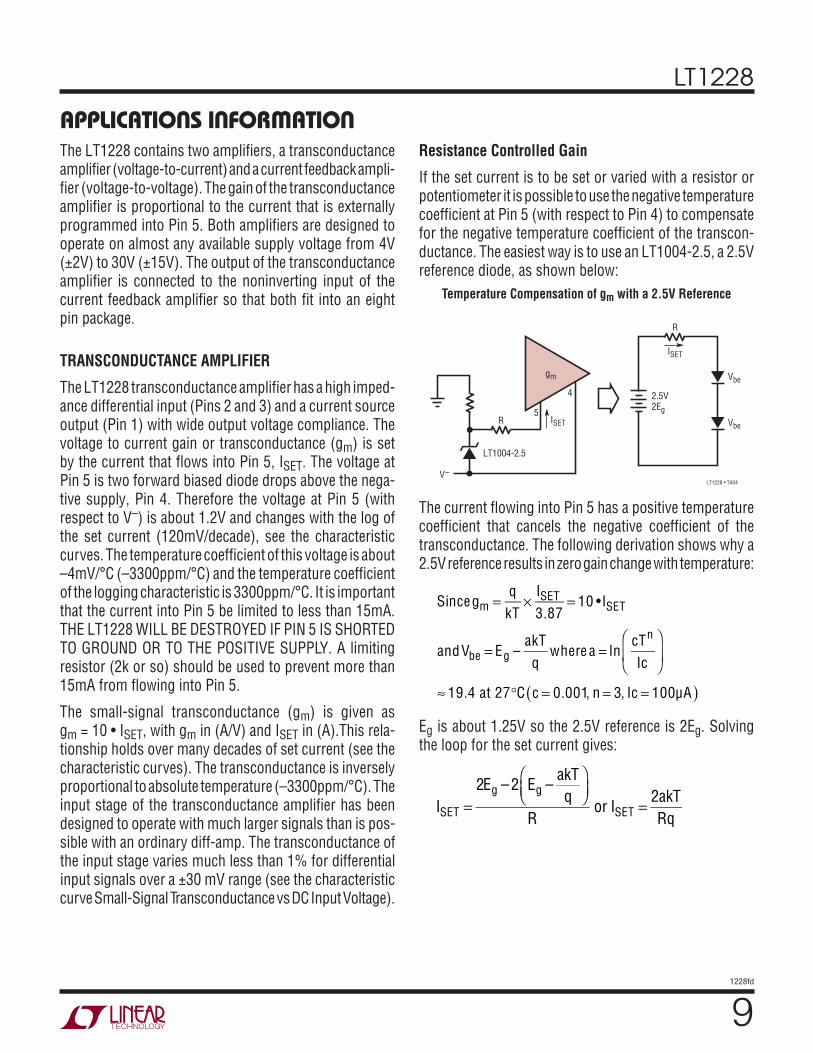
Resistance Controlled Gain
If the set current is to be set or varied with a resistor or potentiometer it is possible to use the negative temperature coefficient at Pin 5 (with respect to Pin 4) to compensate for the negative temperature coefficient of the transcon-ductance. The easiest way is to use an LT1004-2.5, a 2.5V reference diode, as shown below:
Temperature Compensation of gm with a 2.5V Reference
LT1228 • TA04
LT1004-2.5
V–
gm
5
4
R ISET
ISET
R
Vbe
Vbe
2.5V2Eg
The current flowing into Pin 5 has a positive temperature coefficient that cancels the negative coefficient of the transconductance. The following derivation shows why a 2.5V reference results in zero gain change with temperature:
Sincegm =q
kT×
ISET3.87
= 10 •ISET
and Vbe = Eg –akTq
where a = IncTn
Ic
≈ 19.4 at 27°C c = 0.001, n = 3, Ic = 100µA( )
Eg is about 1.25V so the 2.5V reference is 2Eg. Solving the loop for the set current gives:
ISET =
2Eg – 2 Eg –akTq
Ror ISET = 2akT
Rq

LT1228
101228fd
APPLICATIONS INFORMATIONSubstituting into the equation for transconductance gives:
gm = a
1.94R= 10
R
The temperature variation in the term “a” can be ignored since it is much less than that of the term “T” in the equa-tion for Vbe. Using a 2.5V source this way will maintain the gain constant within 1% over the full temperature range of –55°C to 125°C. If the 2.5V source is off by 10%, the gain will vary only about ±6% over the same temperature range.
We can also temperature compensate the transconductance without using a 2.5V reference if the negative power supply is regulated. A Thevenin equivalent of 2.5V is generated from two resistors to replace the reference. The two resis-tors also determine the maximum set current, approxi-mately 1.1V/RTH. By rearranging the Thevenin equations to solve for R4 and R6 we get the following equations in terms of RTH and the negative supply, VEE.
R4 = RTH
1–2.5VVEE
and R6 = RTHVEE2.5V
Temperature Compensation of gm with a Thevenin Voltage
diode drops above the negative supply, a single resistor from the control voltage source to Pin 5 will suffice in many applications. The control voltage is referenced to the negative supply and has an offset of about 900mV. The conversion will be monotonic, but the linearity is determined by the change in the voltage at Pin 5 (120mV per decade of current). The characteristic is very repeat-able since the voltage at Pin 5 will vary less than ±5% from part to part. The voltage at Pin 5 also has a negative temperature coefficient as described in the previous sec-tion. When the gain of several LT1228s are to be varied together, the current can be split equally by using equal value resistors to each Pin 5.
For more accurate (and linear) control, a voltage-to-current converter circuit using one op amp can be used. The fol-lowing circuit has several advantages. The input no longer has to be referenced to the negative supply and the input can be either polarity (or differential). This circuit works on both single and split supplies since the input voltage and the Pin 5 voltage are independent of each other. The temperature coefficient of the output current is set by R5.
LT1228 • TA05
R41.24kΩ
–15V
gm
5
4
R' ISET
ISET
1.03k
Vbe
Vbe
VTH = 2.5V
R'
R66.19kΩ
Voltage Controlled Gain
To use a voltage to control the gain of the transconductance amplifier requires converting the voltage into a current that flows into Pin 5. Because the voltage at Pin 5 is two
LT1228 • TA19
R51k
R11M
V1
V2
IOUTTO PIN 5OF LT1228
50pF
R1 = R2R3 = R4
IOUT = • = 1mA/V
–
+R21M
R31M
R41M
(V1 – V2)R5
R3R1
LT1006
Digital control of the transconductance amplifier gain is done by converting the output of a DAC to a current flow-ing into Pin 5. Unfortunately most current output DACs sink rather than source current and do not have output

LT1228
111228fd
APPLICATIONS INFORMATIONcompliance compatible with Pin 5 of the LT1228. There-fore, the easiest way to digitally control the set current is to use a voltage output DAC and a voltage-to-current circuit. The previous voltage-to-current converter will take the output of any voltage output DAC and drive Pin 5 with a proportional current. The R, 2R CMOS multiplying DACs operating in the voltage switching mode work well on both single and split supplies with the above circuit.
Logarithmic control is often easier to use than linear control. A simple circuit that doubles the set current for each additional volt of input is shown in the voltage controlled state variable filter application near the end of this data sheet.
Transconductance Amplifier Frequency Response
The bandwidth of the transconductance amplifier is a function of the set current as shown in the characteristic curves. At set currents below 100µA, the bandwidth is approximately:
–3dB bandwidth = 3 • 1011 ISET
The peak bandwidth is about 80MHz at 500µA. When a resistor is used to convert the output current to a volt-age, the capacitance at the output forms a pole with the resistor. The best case output capacitance is about 5pF with ±15V supplies and 6pF with ±5V supplies. You must add any PC board or socket capacitance to these values to get the total output capacitance. When using a 1k resistor at the output of the transconductance amp, the output capacitance limits the bandwidth to about 25MHz.
The output slew rate of the transconductance amplifier is the set current divided by the output capacitance, which is 6pF plus board and socket capacitance. For example with the set current at 1mA, the slew rate would be over 100V/µs.
Transconductance Amp Small-Signal ResponseISET = 500µA, R1 = 50Ω
CURRENT FEEDBACK AMPLIFIER
The LT1228 current feedback amplifier has very high noninverting input impedance and is therefore an excellent buffer for the output of the transconductance amplifier. The noninverting input is at Pin 1, the inverting input at Pin 8 and the output at Pin 6. The current feedback ampli-fier maintains its wide bandwidth for almost all voltage gains making it easy to interface the output levels of the transconductance amplifier to other circuitry. The cur-rent feedback amplifier is designed to drive low imped-ance loads such as cables with excellent linearity at high frequencies.
Feedback Resistor Selection
The small-signal bandwidth of the LT1228 current feedback amplifier is set by the external feedback resistors and the internal junction capacitors. As a result, the bandwidth is a function of the supply voltage, the value of the feedback resistor, the closed-loop gain and load resistor. The char-acteristic curves of bandwidth versus supply voltage are done with a heavy load (100Ω) and a light load (1k) to

LT1228
121228fd
APPLICATIONS INFORMATIONshow the effect of loading. These graphs also show the family of curves that result from various values of the feedback resistor. These curves use a solid line when the response has less than 0.5dB of peaking and a dashed line for the response with 0.5dB to 5dB of peaking. The curves stop where the response has more than 5dB of peaking.
Current Feedback Amp Small-Signal ResponseVS = ±15V, RF = RG = 750Ω, RL = 100Ω
Capacitance on the Inverting Input
Current feedback amplifiers want resistive feedback from the output to the inverting input for stable operation. Take care to minimize the stray capacitance between the output and the inverting input. Capacitance on the inverting input to ground will cause peaking in the frequency response (and overshoot in the transient response), but it does not degrade the stability of the amplifier. The amount of capacitance that is necessary to cause peaking is a func-tion of the closed-loop gain taken. The higher the gain, the more capacitance is required to cause peaking. For example, in a gain of 100 application, the bandwidth can be increased from 10MHz to 17MHz by adding a 2200pF capacitor, as shown below. CG must have very low series resistance, such as silver mica.
At a gain of two, on ±15V supplies with a 750Ω feedback resistor, the bandwidth into a light load is over 160MHz without peaking, but into a heavy load the bandwidth re-duces to 100MHz. The loading has so much effect because there is a mild resonance in the output stage that enhances the bandwidth at light loads but has its Q reduced by the heavy load. This enhancement is only useful at low gain settings, at a gain of ten it does not boost the bandwidth. At unity gain, the enhancement is so effective the value of the feedback resistor has very little effect on the bandwidth. At very high closed-loop gains, the bandwidth is limited by the gain-bandwidth product of about 1GHz. The curves show that the bandwidth at a closed-loop gain of 100 is 10MHz, only one tenth what it is at a gain of two.
LT1228 • TA08
–
+
CGRG5.1Ω
RF510Ω
VOUTCFA
VIN6
1
8
Boosting Bandwidth of High Gain Amplifierwith Capacitance On Inverting Input
FREQUENCY (MHz)
119
GAIN
(dB)
22
25
28
31
46
49
10 100
LT1228 • TA09
34
37
40
43CG = 4700pF
CG = 2200pF
CG = 0

LT1228
131228fd
APPLICATIONS INFORMATIONCapacitive Loads
The LT1228 current feedback amplifier can drive capacitive loads directly when the proper value of feedback resistor is used. The graph of Maximum Capacitive Load vs Feedback Resistor should be used to select the appropriate value. The value shown is for 5dB peaking when driving a 1k load, at a gain of 2. This is a worst case condition, the amplifier is more stable at higher gains, and driving heavier loads. Alternatively, a small resistor (10Ω to 20Ω) can be put in series with the output to isolate the capacitive load from the amplifier output. This has the advantage that the amplifier bandwidth is only reduced when the capacitive load is present and the disadvantage that the gain is a function of the load resistance.
Slew Rate
The slew rate of the current feedback amplifier is not inde-pendent of the amplifier gain configuration the way it is in a traditional op amp. This is because the input stage and the output stage both have slew rate limitations. The input stage of the LT1228 current feedback amplifier slews at about 100V/µs before it becomes nonlinear. Faster input signals will turn on the normally reverse biased emitters on the input transistors and enhance the slew rate significantly. This enhanced slew rate can be as much as 3500V/µs!
Current Feedback Amp Large-Signal ResponseVS = ±15V, RF = RG = 750Ω Slew Rate Enhanced
The output slew rate is set by the value of the feedback resistors and the internal capacitance. At a gain of ten with a 1k feedback resistor and ±15V supplies, the output slew rate is typically 500V/µs and –850V/µs. There is no input stage enhancement because of the high gain. Larger feed-back resistors will reduce the slew rate as will lower supply voltages, similar to the way the bandwidth is reduced.
Current Feedback Amp Large-Signal ResponseVS = ±15V, RF = 1k, RG = 110Ω, RL = 400Ω
Settling Time
The characteristic curves show that the LT1228 current feedback amplifier settles to within 10mV of final value in 40ns to 55ns for any output step less than 10V. The curve of settling to 1mV of final value shows that there is a slower thermal contribution up to 20µs. The thermal settling component comes from the output and the input stage. The output contributes just under 1mV/V of output change and the input contributes 300µV/V of input change. Fortunately the input thermal tends to cancel the output thermal. For this reason the noninverting gain of two configuration settles faster than the inverting gain of one.

LT1228
141228fd
Power Supplies
The LT1228 amplifiers will operate from single or split supplies from ±2V (4V total) to ±18V (36V total). It is not necessary to use equal value split supplies, however the offset voltage and inverting input bias current of the current feedback amplifier will degrade. The offset voltage changes about 350µV/V of supply mismatch, the inverting bias current changes about 2.5µA/V of supply mismatch.
Power Dissipation
The worst case amplifier power dissipation is the total of the quiescent current times the total power supply voltage plus the power in the IC due to the load. The quiescent supply current of the LT1228 transconductance amplifier is equal to 3.5 times the set current at all temperatures. The quiescent supply current of the LT1228 current feedback amplifier has a strong negative temperature coefficient and at 150°C is less than 7mA, typically only 4.5mA. The power in the IC due to the load is a function of the output voltage, the supply voltage and load resistance. The worst case occurs when the output voltage is at half supply, if it can go that far, or its maximum value if it cannot reach half supply.
APPLICATIONS INFORMATION
TYPICAL APPLICATIONS
For example, let’s calculate the worst case power dis-sipation in a variable gain video cable driver operating on ±12V supplies that delivers a maximum of 2V into 150Ω. The maximum set current is 1mA.
PD = 2VS ISMAX + 3.5ISET( ) + VS – VOMAX( ) VOMAXRL
PD = 2 •12V • 7mA + 3.5 •1mA( ) + 12V – 2V( ) 2V150Ω
= 0.252 + 0.133 = 0.385W
The total power dissipation times the thermal resistance of the package gives the temperature rise of the die above ambient. The above example in SO-8 surface mount pack-age (thermal resistance is 150°C/W) gives:
Temperature Rise = PDθJA = 0.385W • 150°C/W = 57.75°C
Therefore the maximum junction temperature is 70°C +57.75°C or 127.75°C, well under the absolute maximum junction temperature for plastic packages of 150°C.
Basic Gain Control
The basic gain controlled amplifier is shown on the front page of the data sheet. The gain is directly proportional to the set current. The signal passes through three stages from the input to the output.
First the input signal is attenuated to match the dynamic range of the transconductance amplifier. The attenuator should reduce the signal down to less than 100mV peak. The characteristic curves can be used to estimate how much distortion there will be at maximum input signal. For single ended inputs eliminate R2A or R3A.
The signal is then amplified by the transconductance amplifier (gm) and referred to ground. The voltage gain of the transconductance amplifier is:
gm • R1 = 10 • ISET • R1
Lastly the signal is buffered and amplified by the current feedback amplifier (CFA). The voltage gain of the current feedback amplifier is:
1+ RF
RG
The overall gain of the gain controlled amplifier is the product of all three stages:
AV = R3
R3+R3A
•10 •ISET •R1• 1+ RF
RG
More than one output can be summed into R1 because the output of the transconductance amplifier is a current. This is the simplest way to make a video mixer.

LT1228
151228fd
TYPICAL APPLICATIONSVideo Fader Video DC Restore (Clamp) Circuit
LT1228 • TA12
–
+–
+1k
100Ω
gm
LT1223CFA VOUT
3
2
5
1VIN1
1k
–
+gm
31kVIN2
10k
5.1k10k
5.1k10k
100Ω
2
1k
5
1
–5V VS = ±5V
The video fader uses the transconductance amplifiers from two LT1228s in the feedback loop of another cur-rent feedback amplifier, the LT1223. The amount of signal from each input at the output is set by the ratio of the set currents of the two LT1228s, not by their absolute value. The bandwidth of the current feedback amplifier is inversely proportional to the set current in this configuration. Therefore, the set currents remain high over most of the pot’s range, keeping the bandwidth over 15MHz even when the signal is attenuated 20dB. The pot is set up to completely turn off one LT1228 at each end of the rotation.
LT1228 • TA13
–
+–
+gm
CFA VOUT8
3
25
V–
3k
RF
RG
4 10k
3k
5V
LOGICINPUT
RESTORE
0.01µF
VIDEOINPUT
2N3906
1
6
V+
7
200Ω1000pF
NOT NECESSARY IF THE SOURCE RESISTANCE IS LESS THAN 50Ω
The video restore (clamp) circuit restores the black level of the composite video to zero volts at the beginning of every line. This is necessary because AC coupled video changes DC level as a function of the average brightness of the picture. DC restoration also rejects low frequency noise such as hum.
The circuit has two inputs: composite video and a logic signal. The logic signal is high except during the back porch time right after the horizontal sync pulse. While the logic is high, the PNP is off and ISET is zero. With ISET equal to zero the feedback to Pin 2 has no affect. The video input drives the noninverting input of the current feedback amplifier whose gain is set by RF and RG. When the logic signal is low, the PNP turns on and ISET goes to about 1mA. Then the transconductance amplifier charges the capacitor to force the output to match the voltage at Pin 3, in this case zero volts.
This circuit can be modified so that the video is DC coupled by operating the amplifier in an inverting configuration. Just ground the video input shown and connect RG to the video input instead of to ground.

LT1228
161228fd
Single Supply Wien Bridge Oscillator
TYPICAL APPLICATIONS
LT1228 • TA15
–
+–
+gm
CFAVO
8
3
2
1k
330Ω
4
1
6
V+
7
1k
30pF
51Ω
50Ω
VO = 10dB
AT VS = ±5V ALL HARMONICS 40dB DOWNAT VS = ±12V ALL HARMONICS 50dB DOWN
9.1k
750ΩV–
5
4.3k4.7µH
10k 0.1µF
V–
2N3904
2N3906
In this application the LT1228 is biased for operation from a single supply. An artificial signal ground at half supply voltage is generated with two 10k resistors and bypassed with a capacitor. A capacitor is used in series with RG to set the DC gain of the current feedback amplifier to unity.
The transconductance amplifier is used as a variable resistor to control gain. A variable resistor is formed by driving the inverting input and connecting the output back to it. The equivalent resistor value is the inverse of the gm. This works with the 1.8k resistor to make a variable attenuator. The 1MHz oscillation frequency is set by the Wien bridge network made up of two 1000pF capacitors and two 160Ω resistors.
For clean sine wave oscillation, the circuit needs a net gain of one around the loop. The current feedback amplifier has a gain of 34 to keep the voltage at the transconductance amplifier input low. The Wien bridge has an attenuation of
3 at resonance; therefore the attenuation of the 1.8k resis-tor and the transconductance amplifier must be about 11, resulting in a set current of about 600µA at oscillation. At start-up there is no set current and therefore no attenuation for a net gain of about 11 around the loop. As the output oscillation builds up it turns on the PNP transistor which generates the set current to regulate the output voltage.
12MHz Negative Resistance LC Oscillator
LT1228 • TA14
–
+–
+gm
CFA
VO
8
3
2
5
RF680Ω
RG20Ω
4
1
6
V+
710kΩ
10kΩ
1.8k
160Ω
1000pF 1000pF160Ω
+10µF+
10µF
V+
470Ω +10µF
100Ω
0.1µF
51Ω
50Ω
2N3906
6V TO 30V
f = 1MHz
FOR 5V OPERATION SHORT OUT 100Ω RESISTOR
VO = 6dBm (450mVRMS)2nd HARMONIC = –38dBc3rd HARMONIC = –54dBc
This oscillator uses the transconductance amplifier as a negative resistor to cause oscillation. A negative resistor results when the positive input of the transconductance amplifier is driven and the output is returned to it. In this example a voltage divider is used to lower the signal level at the positive input for less distortion. The negative resistor will not DC bias correctly unless the output of the transconductance amplifier drives a very low resistance. Here it sees an inductor to ground so the gain at DC is zero. The oscillator needs negative resistance to start and that is provided by the 4.3k resistor to Pin 5. As the output level rises it turns on the PNP transistor and in turn the NPN which steals current from the transconductance amplifier bias input.

LT1228
171228fd
TYPICAL APPLICATIONSFilters
LT1228 • TA16
–
+–
+gm
CFA VOUT8
3
2
RF1k
R2120Ω
5
1
6R3
120Ω C330pF
fC = × × ×
R3A1k
ISET RG1k
R2A1k
VINLOWPASS
INPUT
VINHIGHPASS
INPUT
fC = 109 ISET FOR THE VALUES SHOWN
102π
ISETC
RF + 1RG
R2R2 + R2A
Single Pole Low/High/Allpass Filter
Allpass Filter Phase Response
FREQUENCY (Hz)
10k
PHAS
E SH
IFT
(DEG
REES
)
–90
–45
0
100k 1M 10M
LT1228 • TA17
–135
–180
1mA SET CURRENT
100µA SET CURRENT
Using the variable transconductance of the LT1228 to make variable filters is easy and predictable. The most straight forward way is to make an integrator by putting a capacitor at the output of the transconductance amp and buffering it with the current feedback amplifier. Because the input bias current of the current feedback amplifier must be supplied by the transconductance amplifier, the set current should not be operated below 10µA. This limits the filters to about a 100:1 tuning range.
The Single Pole circuit realizes a single pole filter with a corner frequency (fC) proportional to the set current. The
values shown give a 100kHz corner frequency for 100µA set current. The circuit has two inputs, a lowpass filter input and a highpass filter input. To make a lowpass filter, ground the highpass input and drive the lowpass input. Conversely for a highpass filter, ground the lowpass input and drive the highpass input. If both inputs are driven, the result is an allpass filter or phase shifter. The allpass has flat amplitude response and 0° phase shift at low frequen-cies, going to –180° at high frequencies. The allpass filter has –90° phase shift at the corner frequency.

LT1228
181228fd
TYPICAL APPLICATIONSVoltage Controlled State Variable Filter
LT1228 • TA18
–
+–
+gm
CFALOWPASSOUTPUT
8
3
2
1k
4
1
6100Ω
18pF
–5V
3.3k
7
5
–
+–
+gm
CFABANDPASSOUTPUT8
3
2
1k
4
1
6
100Ω
18pF–5V
3.3k 7
5
100Ω
VIN
5V
5V
3k
3k
–
+
100pF
LT10061k
180Ω
10kVC
51k
–5V
2N3906
3.3k
3.3k
fO = 100kHz AT VC = 0VfO = 200kHz AT VC = 1VfO = 400kHz AT VC = 2VfO = 800kHz AT VC = 3VfO = 1.6MHz AT VC = 4V
The state variable filter has both lowpass and bandpass outputs. Each LT1228 is configured as a variable integrator whose frequency is set by the attenuators, the capacitors and the set current. Because the integrators have both positive and negative inputs, the additional op amp nor-mally required is not needed. The input attenuators set the circuit up to handle 3VP–P signals.
The set current is generated with a simple circuit that gives logarithmic voltage to current control. The two PNP transistors should be a matched pair in the same package
for best accuracy. If discrete transistors are used, the 51k resistor should be trimmed to give proper frequency response with VC equal zero. The circuit generates 100µA for VC equal zero volts and doubles the current for every additional volt. The two 3k resistors divide the current between the two LT1228s. Therefore the set current of each amplifier goes from 50µA to 800µA for a control voltage of 0V to 4V. The resulting filter is at 100kHz for VC equal zero, and changes it one octave/V of control input.

LT1228
191228fd
PACKAGE DESCRIPTIONPlease refer to http://www.linear.com/designtools/packaging/ for the most recent package drawings.
J8 0801
.014 – .026(0.360 – 0.660)
.200(5.080)
MAX
.015 – .060(0.381 – 1.524)
.1253.175MIN
.100(2.54)BSC
.300 BSC(7.62 BSC)
.008 – .018(0.203 – 0.457)
0° – 15°
.005(0.127)
MIN
.405(10.287)
MAX
.220 – .310(5.588 – 7.874)
1 2 3 4
8 7 6 5
.025(0.635)
RAD TYP.045 – .068
(1.143 – 1.650)FULL LEAD
OPTION
.023 – .045(0.584 – 1.143)
HALF LEADOPTION
CORNER LEADS OPTION (4 PLCS)
.045 – .065(1.143 – 1.651)NOTE: LEAD DIMENSIONS APPLY TO SOLDER DIP/PLATE
OR TIN PLATE LEADS
J8 Package3-Lead CERDIP (Narrow .300 Inch, Hermetic)
(Reference LTC DWG # 05-08-1110)
OBSOLETE PACKAGE

LT1228
201228fd
PACKAGE DESCRIPTIONPlease refer to http://www.linear.com/designtools/packaging/ for the most recent package drawings.
.016 – .050(0.406 – 1.270)
.010 – .020(0.254 – 0.508)
× 45°
0°– 8° TYP.008 – .010
(0.203 – 0.254)
SO8 REV G 0212
.053 – .069(1.346 – 1.752)
.014 – .019(0.355 – 0.483)
TYP
.004 – .010(0.101 – 0.254)
.050(1.270)
BSC
1 2 3 4
.150 – .157(3.810 – 3.988)
NOTE 3
8 7 6 5
.189 – .197(4.801 – 5.004)
NOTE 3
.228 – .244(5.791 – 6.197)
.245MIN .160 ±.005
RECOMMENDED SOLDER PAD LAYOUT
.045 ±.005 .050 BSC
.030 ±.005 TYP
INCHES(MILLIMETERS)
NOTE:1. DIMENSIONS IN
2. DRAWING NOT TO SCALE3. THESE DIMENSIONS DO NOT INCLUDE MOLD FLASH OR PROTRUSIONS. MOLD FLASH OR PROTRUSIONS SHALL NOT EXCEED .006" (0.15mm)4. PIN 1 CAN BE BEVEL EDGE OR A DIMPLE
S8 Package8-Lead Plastic Small Outline (Narrow .150 Inch)
(Reference LTC DWG # 05-08-1610 Rev G)
N8 REV I 0711
.065(1.651)
TYP
.045 – .065(1.143 – 1.651)
.130 ±.005(3.302 ±0.127)
.020(0.508)
MIN.018 ±.003(0.457 ±0.076)
.120(3.048)
MIN
.008 – .015(0.203 – 0.381)
.300 – .325(7.620 – 8.255)
.325+.035–.015+0.889–0.3818.255( )
1 2 3 4
8 7 6 5
.255 ±.015*(6.477 ±0.381)
.400*(10.160)
MAX
NOTE:1. DIMENSIONS ARE
INCHESMILLIMETERS
*THESE DIMENSIONS DO NOT INCLUDE MOLD FLASH OR PROTRUSIONS. MOLD FLASH OR PROTRUSIONS SHALL NOT EXCEED .010 INCH (0.254mm)
.100(2.54)BSC
N Package8-Lead PDIP (Narrow .300 Inch)
(Reference LTC DWG # 05-08-1510 Rev I)
LT1228
211228fd
Information furnished by Linear Technology Corporation is believed to be accurate and reliable. However, no responsibility is assumed for its use. Linear Technology Corporation makes no representa-tion that the interconnection of its circuits as described herein will not infringe on existing patent rights.
REVISION HISTORYREV DATE DESCRIPTION PAGE NUMBER
D 06/12 Updated Order Information table to new formatClarified units used in gm = 10 • ISET relationship
2 9
(Revision history begins at Rev D)
LT1228
221228fd
Linear Technology Corporation1630 McCarthy Blvd., Milpitas, CA 95035-7417 (408) 432-1900 FAX: (408) 434-0507 www.linear.com LINEAR TECHNOLOGY CORPORATION 2012
LT 0612 REV D • PRINTED IN USA
RELATED PARTS
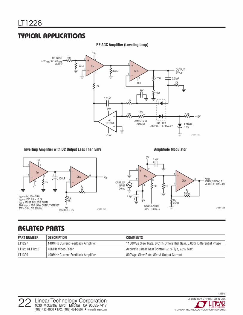
TYPICAL APPLICATIONSRF AGC Amplifier (Leveling Loop)
+
–A3
LT1006
LT1228 • TA20
+
–CFA
100Ω
10kRF INPUT0.6VRMS to 1.3VRMS
25MHz
300Ω
–15V
15V
+
–gm
470Ω
10Ω
0.01µF
10k
0.01µF
15V
–15V
4pF
10k
100k
AMPLITUDEADJUST
10k 4.7k–15V
LT10041.2V
10k
OUTPUT2VP–P
1N4148’s COUPLE THERMALLY
3
2
7
5
1
84
Inverting Amplifier with DC Output Less Than 5mV Amplitude Modulator
LT1228 • TA21
–
+ +100µF
–
+
R5
V–
gm3
2
V+
7
5
4
1
8
6VOCFA
RF1k
RG1k
VS = ±5V, R5 = 3.6kVS = ±15V, R5 = 13.6kVOUT MUST BE LESS THAN200mVP–P FOR LOW OUTPUT OFFSETBW = 30Hz TO 20MHz VIN
INCLUDES DCLT1228 • TA22
–
+
1k –
+
10k
–5V
gm
3
5V
7
5
4
1
8
6 VOUT0dBm(230mV) ATMODULATION = 0V
CFA
RF750Ω
RG750Ω
+
+4.7µF
MODULATIONINPUT ≤ 8VP–P
4.7µF
CARRIERINPUT30mV
2
PART NUMBER DESCRIPTION COMMENTS
LT1227 140MHz Current Feedback Amplifier 1100V/µs Slew Rate, 0.01% Differential Gain, 0.03% Differential Phase
LT1251/LT1256 40MHz Video Fader Accurate Linear Gain Control: ±1% Typ, ±3% Max
LT1399 400MHz Current Feedback Amplifier 800V/µs Slew Rate, 80mA Output Current