
lt1054
16
1 LT1054 Switched-Capacitor Voltage Converter with Regulator S FE ATUR E D ESCRIPTIO s Available in Space Saving SO-8 Package s Output Current: 100mA s Low Loss: 1.1V at 100mA s Operating Range: 3.5V to 15V s Reference and Error Amplifier for Regulation s External Shutdown s External Oscillator Synchronization s Can Be Paralleled s Pin Compatible with the LTC ® 1044/LTC7660 The LT ® 1054 is a monolithic, bipolar, switched-capacitor voltage converter and regulator. The LT1054 provides higher output current than previously available converters with significantly lower voltage losses. An adaptive switch driver scheme optimizes efficiency over a wide range of output currents. Total voltage loss at 100mA output current is typically 1.1V. This holds true over the full supply voltage range of 3.5V to 15V. Quiescent current is t ypically 2.5mA. The LT1054 also provides regulation, a feature not previ- ously available in switched-capacitor voltage converters. By adding an external resistive divider a regulated output can be obtained. This output will be regulated against changes in both input voltage and output current. The LT1054 can also be shut down by grounding the feedback pin. Supply current in shutdown is less than 100 µ A. The internal oscillator of the LT1054 runs at a nominal frequency of 25kHz. The oscillator pin can be used to adjust the switching frequency or to externally synchronize the LT1054. The LT1054 is pin compatible with previous converters such the LTC1044/LTC7660. s Voltage Inverter s Voltage Regulator s Negative Voltage Doubler s Positive Voltage Doubler S A O PP LIC ATI , LTC and LT are registered trademarks of Linear Technology Corporation. BLOCK DIAGRAM OUTPUT CURRENT (mA) 0 V O L T A G E L O S S ( V ) 1 2 40 LT1054 • TA01 0 10 20 30 50 60 70 80 90 100 3.5V ≤ V IN ≤ 15V C IN = C OUT = 100µF INDICATES GUARANTEED TEST POINT T J = 125°C T J = 25°C T J = –55°C REFERENCE OSC DRIVE DRIVE DRIVE DRIVE OSC CAP – GND CAP + FEEDBACK/ SHUTDOWN – + R R *EXTERNAL CAPACITORS 2.5V 6 1 4 3 –V OUT LT1054 • BD 5 2 8 7 Q Q V REF C IN * V IN C OUT * + Voltage Loss
-
Upload
francimora -
Category
Documents
-
view
218 -
download
0
Transcript of lt1054

8/3/2019 lt1054
http://slidepdf.com/reader/full/lt1054 1/161
LT1054
Switched-Capacitor VoltageConverter with Regulator
SFEATURE DU
ESCRIPTIO
s Available in Space Saving SO-8 Packages Output Current: 100mAs Low Loss: 1.1V at 100mAs Operating Range: 3.5V to 15Vs Reference and Error Amplifier for Regulations External Shutdowns External Oscillator Synchronizations Can Be Paralleleds Pin Compatible with the LTC®1044/LTC7660
The LT®1054 is a monolithic, bipolar, switched-capacitorvoltage converter and regulator. The LT1054 provideshigher output current than previously available converterswith significantly lower voltage losses. An adaptive switchdriver scheme optimizes efficiency over a wide range ofoutput currents. Total voltage loss at 100mA output currentis typically 1.1V. This holds true over the full supply voltagerange of 3.5V to 15V. Quiescent current is typically 2.5mA.
The LT1054 also provides regulation, a feature not previ-ously available in switched-capacitor voltage converters.By adding an external resistive divider a regulated outputcan be obtained. This output will be regulated againstchanges in both input voltage and output current. TheLT1054 can also be shut down by grounding the feedbackpin. Supply current in shutdown is less than 100µA.
The internal oscillator of the LT1054 runs at a nominalfrequency of 25kHz. The oscillator pin can be used to adjustthe switching frequency or to externally synchronize theLT1054.
The LT1054 is pin compatible with previous converters
such the LTC1044/LTC7660.
s Voltage Inverters Voltage Regulators Negative Voltage Doublers Positive Voltage Doubler
USA
OPPLICATI
, LTC and LT are registered trademarks of Linear Technology Corporation.
BLOCK DIAGRAM W
OUTPUT CURRENT (mA)
0
V O L T A G E L O S S ( V )
1
2
40
LT1054 • TA01
010 20 30 50 60 70 80 90 100
3.5V ≤ VIN ≤ 15VCIN = COUT = 100µF
INDICATES GUARANTEED TEST POINT
TJ = 125°CTJ = 25°CTJ = –55°C
REFERENCE
OSC
DRIVE DRIVE
DRIVE
DRIVE
OSC
CAP–
GND
CAP +
FEEDBACK/
SHUTDOWN
–
+
R
R
*EXTERNAL CAPACITORS
2.5V
6
1
4
3
–VOUT
LT1054 • BD
5
2
8
7
Q
Q
VREF
CIN*
VIN
+
COUT*+
Voltage Loss

8/3/2019 lt1054
http://slidepdf.com/reader/full/lt1054 2/162
LT1054
AUG
WA
WU
WARBSOLUTE XI TI S
Supply Voltage (Note 1) .......................................... 16VInput Voltage
Pin 1 ................................................. 0V ≤ VPIN1 ≤ V+
Pin 3 (S Package) ............................. 0V ≤ VPIN3 ≤ V+
Pin 7 ............................................. 0V ≤ VPIN7 ≤ VREFPin 13 (S Package) ...................... 0V ≤ VPIN13 ≤ VREF
Operating Temperature RangeLT1054C ................................................. 0°C to 70°CLT1054I ............................................. – 40°C to 85°CLT1054M ......................................... –55°C to 125°C
Junction Temperature Range (Note 2)LT1054C .......................................................... 125°CLT1054I ............................................................ 125°C
LT1054M ......................................................... 150°CStorage Temperature Range
H, J8, N8 and S8 Packages................ –55°C to 150°CS Package........................................ –65°C to 150°C
Lead Temperature (Soldering, 10 sec) ................. 300°C
W U UPACKAGE / ORDER I FOR ATIO
ORDER PARTNUMBER
ORDER PARTNUMBER
LT1054CHLT1054MH
TJMAX = 150°C, θJA = 150°C, θJC = 45°C/W
TOP VIEW
OSC
V+
FB/SHDN
VREF
VOUTGND
CAP–CASE
ISVOUT
CAP+
87
6
53
2
1
4
H PACKAGE8-LEAD TO-5 METAL CAN
TJMAX = XXX°C, θJA = XXX°C/W
LT1054CS8
S8 PARTMARKING
1054
ORDER PARTNUMBER
LT1054CJ8LT1054CN8LT1054IN8LT1054MJ8
1
2
3
4
5
6
7
8
TOP VIEW
S PACKAGE16-LEAD PLASTIC SOL
16
15
14
13
12
11
10
9
NC
NC
FB/SHDN
CAP+
GND
CAP–
NC
NC
NC
NC
V+
OSC
VREF
VOUT
NC
NC
TJMAX = 125°C, θJA = 150°C/ W
ORDER PARTNUMBER
LT1054CSLT1054IS
1
2
3
4
8
7
6
5
TOP VIEW
FB/SHDN
CAP+
GND
CAP–
V+
OSC
VREF
VOUT
N8 PACKAGE8-LEAD PLASTIC DIP
J8 PACKAGE8-LEAD CERAMIC DIP
TJMAX = 150°C, θJA = 100°C/ W (J8)
TJMAX = 125°C, θJA = 130°C/ W (N8)
1
2
3
4
8
7
6
5
TOP VIEW
V+
OSC
VREF
VOUT
FB/SHDN
CAP+
GND
CAP–
S8 PACKAGE8-LEAD PLASTIC SO
SEE REGULATION AND CAPACITOR SELECTION SECTIONSIN THE APPLICATIONS INFORMATION FOR IMPORTANTINFORMATION ON THE S8 DEVICE
(Note 6)
N O T R
E C O M M E N D E
D
F O R N E
W D E S I G N S
U U
U U
W W

8/3/2019 lt1054
http://slidepdf.com/reader/full/lt1054 3/163
LT1054
ELECTRICAL C CHARA TERISTICS
PARAMETER CONDITIONS MIN TYP MAX UNITS
Supply Current ILOAD = 0mAVIN = 3.5V q 2.5 4.0 mA
VIN = 15Vq
3.0 5.0 mASupply Voltage Range q 3.5 15 V
Voltage Loss (VIN – |VOUT|) CIN = COUT = 100µF Tantalum (Note 3)IOUT = 10mA q 0.35 0.55 VIOUT = 100mA q 1.10 1.60 V
Output Resistance ∆IOUT = 10mA to 100mA (Note 4) q 10 15 Ω
Oscillator Frequency 3.5V ≤ VIN ≤ 15V q 15 25 35 kHz
Reference Voltage IREF = 60µA, TJ = 25°C 2.35 2.50 2.65 Vq 2.25 2.75 V
Regulated Voltage VIN = 7V, TJ = 25°C, RL = 500Ω (Note 5) –4.70 –5.00 –5.20 V
Line Regulation 7V ≤ VIN ≤ 12V, RL = 500Ω (Note 5) q 5 25 mV
Load Regulation VIN = 7V, 100Ω ≤ RL ≤ 500Ω (Note 5) q 10 50 mV
Maximum Switch Current 300 mA
Supply Current in Shutdown VPIN1 = 0V q 100 200 µA
Note 4: Output resistance is defined as the slope of the curve, (∆VOUT vs∆IOUT), for output currents of 10mA to 100mA. This represents the linearportion of the curve. The incremental slope of the curve will be higher atcurrents < 10mA due to the characteristics of the switch transistors.
Note 5: All regulation specifications are for a device connected as apositive-to-negative converter/regulator with R1 = 20k, R2 = 102.5k,C1 = 0.002µF, (C1 = 0.05µF S package) CIN = 10µF tantalum,COUT = 100µF tantalum.
Note 6: The S8 package uses a different die than the H, J8, N8 and Spackages. The S8 device will meet all the existing data sheet parameters.See Regulation and Capacitor Selection in the Applications Information
section for differences in application requirements.
The q denotes specifications which apply over the full operatingtemperature range. For C grade parts these specifications also apply up toa junction temperature of 100°C.
Note 1: The absolute maximum supply voltage rating of 16V is forunregulated circuits. For regulation mode circuits with VOUT ≤ 15V atpin 5, (pin 11 S package) this rating may be increased to 20V.
Note 2: The devices are guaranteed by design to be functional up to theabsolute maximum junction temperature.
Note 3: For voltage loss tests, the device is connected as a voltageinverter, with pins 1, 6, and 7 (3, 12, and 13 S package) unconnected.The voltage losses may be higher in other configurations.
C CHARA TERISTICS U W
ATYPICAL PERFOR CE
Shutdown Threshold
TEMPERATURE (°C)
–50–7015
F R E Q U E N
C Y ( k H z )
25
35
0 50 75
LT1054 • TPC03
–25 25 100 125
VIN = 15V
VIN = 3.5V
Oscillator Frequency
INPUT VOLTAGE (V)
00
S U P P L Y C U R
R E N T ( m A )
1
2
3
4
5IL = 0
5 10 15
LT1054 • TPC02
Supply Current
TEMPERATURE (˚C)
–50
S H U T D O W N T H
R E S H O L D ( V )
0.4
0.5
0.6
25 75
LT1054 • TPC01
0.3
0.2
–25 0 50 100 125
0.1
0
VPIN1
(Note 6)

8/3/2019 lt1054
http://slidepdf.com/reader/full/lt1054 4/164
LT1054
C CHARA TERISTICS U W
ATYPICAL PERFOR CE
Output Voltage Loss
OSCILLATOR FREQUENCY (kHz)
10
V O L T A G E L O S S ( V )
1
2
10 100
LT1054 • TPC07
INVERTER CONFIGURATIONCIN = 10µF TANTALUMCOUT = 100µF TANTALUM
IOUT = 100mA
IOUT = 50mA
IOUT = 10mA
OSCILLATOR FREQUENCY (kHz)
10
V O L T A G E L O S S ( V )
1
2
10 100
LT1054 • TPC08
INVERTER CONFIGURATIONCIN = 100µF TANTALUMCOUT = 100µF TANTALUM
IOUT = 100mA
IOUT = 50mA
IOUT = 10mA
Output Voltage Loss
Reference Voltage TemperatureCoefficientRegulated Output Voltage
TEMPERATURE (°C)
–50–12.6
O U T P U T V O
L T A G E ( V )
–12.4
–12.0
–11.8
–11.6
–4.7
–5.0
0 50 75
LT1054 • TPC09
–12.2
–4.9
–4.8
–5.1
–25 25 100 125
TEMPERATURE (°C)
–50–100
R E F E R E N C E V O L T A
G E C H A N G E ( m V )
–80
–40
–20
0
100
40
0 50 75
LT1054 • TPC10
–60
60
80
20
–25 25 100 125
VREF AT 0 = 2.500V
Supply Current in Shutdown Output Voltage LossAverage Input Current
INPUT VOLTAGE (V)
00
Q U I E S C E N T C U R R E N T ( µ A )
20
40
60
80
120
5 10 15
LT1054 • TPC04
100
VPIN1 = 0V
OUTPUT CURRENT (mA)
00
A V E R A G E I N P U T C U R R E N T ( m A )
20
60
80
100
140
LT1050 • TPC05
40
120
40 10020 60 80
INPUT CAPACITANCE (µF)
00
V O L T A G E L O S S ( V )
0.2
0.6
0.8
1.0
1.4
10 50 70
LT1054 • TPC06
0.4
1.2
40 90 10020 30 60 80
INVERTER CONFIGURATIONCOUT = 100µF TANTALUMfOSC = 25kHz
IOUT = 100mA
IOUT = 50mA
IOUT = 10mA

8/3/2019 lt1054
http://slidepdf.com/reader/full/lt1054 5/165
LT1054
PIN FUNCTIONS U U U
V + (Pin 8): Input Supply. The LT1054 alternately chargesCIN to the input voltage when CIN is switched in parallel withthe input supply and then transfers charge to COUT when
CIN is switched in parallel with COUT. Switching occurs atthe oscillator frequency. During the time that CIN is charg-ing, the peak supply current will be approximately equal to2.2 times the output current. During the time that C IN isdelivering charge to COUT the supply current drops toapproximately 0.2 times the output current. An inputsupply bypass capacitor will supply part of the peak inputcurrent drawn by the LT1054 and average out the currentdrawn from the supply. A minimum input supply bypasscapacitor of 2µF, preferably tantalum or some other lowESR type is recommended. A larger capacitor may be
desirable in some cases, for example, when the actual inputsupply is connected to the LT1054 through long leads, orwhen the pulse current drawn by the LT1054 might affectother circuitry through supply coupling.
VOUT (Pin 5): In addition to being the output pin the pin isalso tied to the substrate of the device. Special care mustbe taken in LT1054 circuits to avoid pulling this pinpositive with respect to any of the other pins. Pulling pin5 positive with respect to pin 3 (GND) will forward bias thesubstrate diode which will prevent the device from starting.This condition can occur when the output load driven by theLT1054 is referred to its positive supply (or to some otherpositive voltage). Note that most op amps present just sucha load since their supply currents flow from their V +
terminals to their V– terminals. To prevent start-up prob-lems with this type of load an external transistor must beadded as shown in Figure 1. This will prevent VOUT (pin 5)from being pulled above the ground pin (pin 3) during start-up. Any small, general purpose transistor such as 2N2222or 2N2219 can be used. RX should be chosen to provideenough base drive to the external transistor so that it issaturated under nominal output voltage and maximumoutput current conditions. In some cases an N-channelenhancement mode MOSFET can be used in place of thetransistor.
RX ≤(|VOUT|)β
IOUT
–
+
LOAD
CIN
COUT
LT1054 • F01
IL
V+
RXLT1054
FB/SHDN
CAP+
GND
CAP–
V+
OSC
VREF
VOUT
+
+
IQ
IOUT
Figure 1
VREF (Pin 6): Reference Output. This pin provides a 2.5V
reference point for use in LT1054-based regulator circuits.The temperature coefficient of the reference voltage hasbeen adjusted so that the temperature coefficient of theregulated output voltage is close to zero. This requires thereference output to have a positive temperature coefficientas can be seen in the typical performance curves. Thisnonzero drift is necessary to offset a drift term inherent inthe internal reference divider and comparator network tiedto the feedback pin. The overall result of these drift terms isa regulated output which has a slight positive temperaturecoefficient at output voltages below 5V and a slight negative
TC at output voltages above 5V. Reference output currentshould be limited, for regulator feedback networks, toapproximately 60µA. The reference pin will draw≈100µA when shorted to ground and will not affect theinternal reference/regulator, so that this pin can also beused as a pull-up for LT1054 circuits that require synchro-nization.
CAP+ /CAP – (Pin 2/Pin 4): Pin 2, the positive side of theinput capacitor (CIN), is alternately driven between V+ andground. When driven to V +, pin 2 sources current from V +.When driven to ground pin 2 sinks current to ground. Pin
4, the negative side of the input capacitor, is driven alter-nately between ground the VOUT. When driven to ground,pin 4 sinks current to ground. When driven to VOUT pin 4sources current from COUT. In all cases current flow in theswitches is unidirectional as should be expected usingbipolar switches.

8/3/2019 lt1054
http://slidepdf.com/reader/full/lt1054 6/166
LT1054
PIN FUNCTIONS U U U
OSC (Pin 7): Oscillator Pin. This pin can be used to raise orlower the oscillator frequency or to synchronize the deviceto an external clock. Internally pin 7 is connected to the
oscillator timing capacitor (Ct ≈150pF) which is alternatelycharged and discharged by current sources of±7µA so thatthe duty cycle is ≈50%. The LT1054 oscillator is designedto run in the frequency band where switching losses areminimized. However the frequency can be raised, lowered,or synchronized to an external system clock if necessary.
The frequency can be lowered by adding an externalcapacitor (C1, Figure 2) from pin 7 to ground. This willincrease the charge and discharge times which lowers theoscillator frequency. The frequency can be increased byadding an external capacitor (C2, Figure 2, in the range of5pF to 20pF) from pin 2 to pin 7. This capacitor will couplecharge into Ct at the switch transitions, which will shortenthe charge and discharge time, raising the oscillator fre-quency. Synchronization can be accomplished by addingan external resistive pull-up from pin 7 to the reference pin(pin 6). A 20k pull-up is recommended. An open collectorgate or an NPN transistor can then be used to drive theoscillator pin at the external clock frequency as shown inFigure 2. Pulling up pin 7 to an external voltage isnot recommended. For circuits that require both fre-
quency synchronization and regulation, an external refer-ence can be used as the reference point for the top of theR1/R2 divider allowing pin 6 to be used as a pull-up point
for pin 7.
FB/SHDN (Pin 1): Feedback/Shutdown Pin. This pin hastwo functions. Pulling pin 1 below the shutdown threshold(≈0.45V) puts the device into shutdown. In shutdown thereference/regulator is turned off and switching stops. Theswitches are set such that both CIN and COUT are dis-charged through the output load. Quiescent current inshutdown drops to approximately 100µA (see TypicalPerformance Characteristics). Any open-collector gate canbe used to put the LT1054 into shutdown. For normal(unregulated) operation the device will start back up whenthe external gate is shut off. In LT1054 circuits that use theregulation feature, the external resistor divider can provideenough pull-down to keep the device in shutdown until theoutput capacitor (COUT) has fully discharged. For mostapplications where the LT1054 would be run intermittently,this does not present a problem because the discharge timeof the output capacitor will be short compared to the off-time of the device. In applications where the device has tostart up before the output capacitor (COUT) has fully dis-charged, a restart pulse must be applied to pin 1 of theLT1054. Using the circuit of Figure 5, the restart signal canbe either a pulse (tp> 100µs) or a logic high. Diode couplingthe restart signal into pin 1 will allow the output voltage tocome up and regulate without overshoot. The resistordivider R3/R4 in Figure 5 should be chosen to provide asignal level at pin 1 of 0.7V to 1.1V.
Pin 1 is also the inverting input of the LT1054’s erroramplifier and as such can be used to obtain a regulatedoutput voltage.Figure 2
VIN
COUT
CIN
C2
+
+
C1
LT1054 • F02
LT1054
FB/SHDN
CAP+
GND
CAP–
V+
OSC
VREF
VOUT

8/3/2019 lt1054
http://slidepdf.com/reader/full/lt1054 7/167
LT1054
APPLICATIONS INFORMATION W U U U
Theory of Operation
To understand the theory of operation of the LT1054, a
review of a basic switched-capacitor building block ishelpful.
In Figure 3 when the switch is in the left position, capacitorC1 will charge to voltage V1. The total charge on C1 will beq1 = C1V1. The switch then moves to the right, dischargingC1 to voltage V2. After this discharge time the charge on C1is q2 = C1V2. Note that charge has been transferred fromthe source V1 to the output V2. The amount of chargetransferred is:
∆q = q1 – q2 = C1(V1 – V2)
If the switch is cycled f times per second, the chargetransfer per unit time (i.e., current) is:
I = f × ∆q = f × C1(V1 – V2)
To obtain an equivalent resistance for the switched-capaci-tor network we can rewrite this equation in terms of voltageand impedance equivalence:
I = =V1 – V2(1/fC1)
V1 – V2REQUIV
f
C1 C2RL
V2
LT1054 • F03
V1
Figure 3. Switched-Capacitor Building Block
A new variable REQUIV is defined such that REQUIV = 1/fC1.Thus the equivalent circuit for the switched-capacitornetwork is as shown in Figure 4. The LT1054 has the sameswitching action as the basic switched-capacitor buildingblock. Even though this simplification doesn’t include finiteswitch on-resistance and output voltage ripple, it provides
an intuitive feel for how the device works.
These simplified circuits explain voltage loss as a functionof frequency (see Typical Performance Characteristics). Asfrequency is decreased, the output impedance will eventu-ally be dominated by the 1/fC1 term and voltage losses willrise.
C2 RL
REQUIV
REQUIV =
V2
LT1054 • F04
V1
1fC1
Figure 4. Switched-Capacitor Equivalent Circuit
Note that losses also rise as frequency increases. This iscaused by internal switching losses which occur due tosome finite charge being lost on each switching cycle. Thischarge loss per-unit-cycle, when multiplied by the switch-ing frequency, becomes a current loss. At high frequencythis loss becomes significant and voltage losses again rise.
The oscillator of the LT1054 is designed to run in the
frequency band where voltage losses are at a minimum.
Regulation
The error amplifier of the LT1054 servos the drive to thePNP switch to control the voltage across the input capaci-tor (CIN) which in turn will determine the output voltage.Using the reference and error amplifier of the LT1054, anexternal resistive divider is all that is needed to set theregulated output voltage. Figure 5 shows the basic regu-lator configuration and the formula for calculating theappropriate resistor values. R1 should be chosen to be
Figure 5
R4
RESTART SHUTDOWN C1
R2
CIN
10µFTANTALUM
COUT100µF
TANTALUM
VOUT
LT1054 • F05
VIN
+
+
R1
2.2µF +
R3
R2R1
= ≈+ 1
WHERE VREF = 2.5V NOMINAL
*CHOOSE THE CLOSEST 1% VALUE
FOR EXAMPLE: TO GET VOUT = –5V REFERRED TO THE GROUND PIN OF THE LT1054, CHOOSE R1 = 20k, THEN
|VOUT| ) )VREF
2– 40mV
R2 = 20k = 102.6k*+ 1|–5V| ) )2.5V
2– 40mV
) ) + 1|VOUT|1.21V
LT1054
FB/SHDN
CAP+
GND
CAP–
V+
OSC
VREF
VOUT

8/3/2019 lt1054
http://slidepdf.com/reader/full/lt1054 8/168
LT1054
APPLICATIONS INFORMATION W U U U
losses will occur on both the charge and discharge cycle.This means that using a capacitor with 1Ω of ESR for CINwill have the same effect as increasing the output imped-
ance of the LT1054 by 4Ω. This represents a significantincrease in the voltage losses. For COUT the affect of ESR isless dramatic. COUT is alternately charged and dischargedat a current approximately equal to the output current andthe ESR of the capacitor will cause a step function to occurin the output ripple at the switch transitions. This stepfunction will degrade the output regulation for changes inoutput load current and should be avoided. Realizing thatlarge value tantalum capacitors can be expensive, a tech-nique that can be used is to parallel a smaller tantalumcapacitor with a large aluminum electrolytic capacitor to
gain both low ESR and reasonable cost. Where physicalsize is a concern some of the newer chip type surfacemount tantalum capacitors can be used. These capacitorsare normally rated at working voltages in the 10V to 20Vrange and exhibit very low ESR (in the range of 0.1Ω).
Output Ripple
The peak-to-peak output ripple is determined by the valueof the output capacitor and the output current. Peak-to-peak output ripple may be approximated by the formula:
dV = IOUT2fCOUT
where dV = peak-to-peak ripple and f = oscillator frequency.
For output capacitors with significant ESR a second termmust be added to account for the voltage step at the switchtransitions. This step is approximately equal to:
(2IOUT)(ESR of COUT)
Power Dissipation
The power dissipation of any LT1054 circuit must belimited such that the junction temperature of the devicedoes not exceed the maximum junction temperature rat-ings. The total power dissipation must be calculated fromtwo components, the power loss due to voltage drops in theswitches and the power loss due to drive current losses.The total power dissipated by the LT1054 can be calculatedfrom:
20k or greater because the reference output current islimited to≈100µA. R2 should be chosen to be in the rangeof 100k to 300k. For optimum results the ratio of CIN /COUT
is recommended to be 1/10. C1, required for good loadregulation at light load currents, should be 0.002µF for alloutput voltages.
A new die layout was required to fit into the physicaldimensions of the S8 package. Although the new die of theLT1054CS8 will meet all the specifications of the existingLT1054 data sheet, subtle differences in the layout of thenew die require consideration in some application cir-cuits. In regulating mode circuits using the 1054CS8 thenominal values of the capacitors, CIN and COUT, must beapproximately equal for proper operation at elevatedjunction temperatures. This is different from the earlierpart. Mismatches within normal production tolerancesfor the capacitors are acceptable. Making the nominalcapacitor values equal will ensure proper operation atelevated junction temperatures at the cost of a smalldegradation in the transient response of regulator cir-cuits. For unregulated circuits the values of CIN and COUTare normally equal for all packages. For S8 applicationsassistance in unusual applications circuits, please consultthe factory.
It can be seen from the circuit block diagram that themaximum regulated output voltage is limited by the supplyvoltage. For the basic configuration, |VOUT| referred to theground pin of the LT1054 must be less than the total of thesupply voltage minus the voltage loss due to the switches.The voltage loss versus output current due to the switchescan be found in Typical Performance Characteristics. Otherconfigurations such as the negative doubler can providehigher output voltages at reduced output currents (seeTypical Applications).
Capacitor SelectionFor unregulated circuits the nominal values of CIN and COUTshould be equal. For regulated circuits see the section onRegulation. While the exact values of CIN and COUT arenoncritical, good quality, low ESR capacitors such as solidtantalum are necessary to minimize voltage losses at highcurrents. For CIN the effect of the ESR of the capacitor willbe multiplied by four due to the fact that switch currents areapproximately two times higher than output current and

8/3/2019 lt1054
http://slidepdf.com/reader/full/lt1054 9/169
LT1054
P ≈ (VIN – |VOUT|)(IOUT) + (VIN)(IOUT)(0.2)
where both VIN and VOUT are referred to the ground pin (pin
3) of the LT1054. For LT1054 regulator circuits, the powerdissipation will be equivalent to that of a linear regulator.Due to the limited power handling capability of the LT1054packages, the user will have to limit output current require-ments or take steps to dissipate some power external to theLT1054 for large input/output differentials. This can beaccomplished by placing a resistor in series with CIN asshown in Figure 6. A portion of the input voltage will thenbe dropped across this resistor without affecting the outputregulation. Because switch current is approximately 2.2
APPLICATIONS INFORMATION W U U U
Figure 6
C1
R2
CIN
COUT
VOUT
LT1054 • F06
VIN
+
+
R1
RX
LT1054
FB/SHDN
CAP+
GND
CAP–
V+
OSC
VREF
VOUT
P = (12V – |–5V|)(100mA) + (12V)(100mA)(0.2)P = 700mW + 240mW = 940mW
At θJA of 130°C/W for a commercial plastic device thiswould cause a junction temperature rise of 122°C so thatthe device would exceed the maximum junction tempera-ture at an ambient temperature of 25°C. Now calculate thepower dissipation with an external resistor (RX). First findhow much voltage can be dropped across RX. The maxi-mum voltage loss of the LT1054 in the standard regulatorconfiguration at 100mA output current is 1.6V, so
VX = 12V – [(1.6V)(1.3) + |– 5V|] = 4.9V andRX = 4.9V/(4.4)(100mA) = 11Ω
This resistor will reduce the power dissipated by theLT1054 by (4.9V)(100mA) = 490mW. The total powerdissipated by the LT1054 would then be = (940mW –490mW) = 450mW. The junction temperature rise wouldnow be only 58°C. Although commercial devices areguaranteed to be functional up to a junction temperatureof 125°C, the specifications are only guaranteed up to ajunction temperature of 100°C, so ideally you should limitthe junction temperature to 100°C. For the above examplethis would mean limiting the ambient temperature to 42°C.Other steps can be taken to allow higher ambient tempera-tures. The thermal resistance numbers for the LT1054
packages represent worst case numbers with no heatsinking and still air. Small clip-on type heat sinks can beused to lower the thermal resistance of the LT1054 pack-age. In some systems there may be some available airflowwhich will help to lower the thermal resistance. Wide PCboard traces from the LT1054 leads can also help toremove heat from the device. This is especially true forplastic packages.
times the output current and the resistor will cause a
voltage drop when CIN is both charging and discharging,the resistor should be chosen as:
RX = VX /(4.4 IOUT)
where
VX ≈ VIN – [(LT1054 Voltage Loss)(1.3) + |VOUT|]
and IOUT = maximum required output current. The factor of1.3 will allow some operating margin for the LT1054.
For example: assume a 12V to –5V converter at 100mAoutput current. First calculate the power dissipation with-
out an external resistor:

8/3/2019 lt1054
http://slidepdf.com/reader/full/lt1054 10/1610
LT1054
TYPICAL APPLICATIONS N U
100mA Regulating Negative Doubler
10µF
10µF
1N4002
HP5082-2810
VIN3.5 TO 15V
20k
1N40020.002µF
LT1054 • TAO6
+
10µF
+
+
2.2µF +
10µF
10µF
R140k
VOUTSET
PIN 2LT1054 #1
–VOUTIOUT ≅ 100mA MAX
R2500k
1N4002
1N4002
1N4002
+
10µF
100µF
+
+
+
, REFER TO FIGURE 5
VIN = 3.5 TO 15VVOUT MAX ≈ –2VIN + [1054 VOLTAGE LOSS + 2(VDIODE)]
R2R1
= =+ 1|VOUT| ) )VREF
2– 40mV ) ) + 1
|VOUT|1.21V
LT1054 #1
FB/SHDN
CAP+
GND
CAP–
V+
OSC
VREF
VOUT
LT1054 #2
FB/SHDN
CAP+
GND
CAP–
V+
OSC
VREF
VOUT
Basic Voltage Inverter/Regulator
0.002µF
R2
10µF
100µF
REFER TO FIGURE 5
2µF
VOUT
LT1054 • TA03
VIN
+
+
+
R1
R2R1
= =+ 1|VOUT| ) )VREF
2– 40mV ) ) + 1 ,
|VOUT|1.21V
LT1054
FB/SHDN
CAP+
GND
CAP–
V+
OSC
VREF
VOUT
Basic Voltage Inverter
100µF
VIN
–VOUT
LT1054 • TAO2
+
+
+
LT1054
FB/SHDN
CAP+
GND
CAP–
V+
OSC
VREF
VOUT
2µF
100µF
Positive Doubler
1N4001
10µF
VIN = 3.5V TO 15VVOUT ≈ 2VIN – (VL + 2VDIODE)VL = LT1054 VOLTAGE LOSS
2µF
VIN3.5V TO 15V
LT1054 • TAO5
+ +
100µF +
1N4001
VOUT
+
–
LT1054
FB/SHDN
CAP+
GND
CAP–
V+
OSC
VREF
VOUT
Negative Voltage Doubler
100µF2µF
VIN = –3.5V TO –15V
VOUT = 2VIN + (LT1054 VOLTAGE LOSS) + (QX SATURATION VOLTAGE)
*SEE FIGURE 3
100µF
VIN
VIN
VOUT
LT1054 • TAO4
QX*
RX*
++
+
+
–LT1054
FB/SHDN
CAP+
GND
CAP–
V+
OSC
VREF
VOUT

8/3/2019 lt1054
http://slidepdf.com/reader/full/lt1054 11/1611
LT1054
TYPICAL APPLICATIONS N U
5V to ±12V Converter
10µF
10µF
1µF
5V
12
3
8
200k
3k
100µFTANTALUM
LT1054 • TAO9
+
+
0.022µF–
+
+
2N2222 A = 125 FOR 0V TO 3V OUT FROM FULL-SCALEBRIDGE OUTPUT OF 24mV
100k
100k
10kZEROTRIM
5kGAINTRIM
10k
10k5V
40Ω
301k 1MA1
1/2 LT1013
5k6
5
4
7
10k
2N2907INPUT TTLOR CMOS
LOW FOR ON
350Ω
–
+
A21/2 LT1013
LT1054
FB/SHDN
CAP+
GND
CAP–
V+
OSC
VREF
VOUT
20k
1N9141N914
100µF
10µF
VIN = 5V
TO PIN 4LT1054 #1
VOUT ≈ –12VIOUT = 25mA
VOUT ≈ 12VIOUT = 25mA
LT1054 • TAO8
+
10µF +
+
+
+
100µF
+
5µF
10µF
+5µF1k
2N2219
+100µF
LT1054 #1
FB/SHDN
CAP+
GND
CAP–
V+
OSC
VREF
VOUT
LT1054 #2
FB/SHDN
CAP+
GND
CAP–
V+
OSC
VREF
VOUT
5V to ±12V Converter
Strain Gauge Bridge Signal Conditioner
100µF
100µF10µF
VIN3.5V TO 15V
–VOUT
LT1054 • TAO7
+
10µF +
+
10µF +
+
+
100µF+VOUT
+
–
+
–
= 1N4001
VIN = 3.5V TO 15V
+VOUT ≈ 2VIN – (VL + 2VDIODE)
–VOUT ≈ –2VIN + (VL + 2VDIODE)
VL = LT1054 VOLTAGE LOSS
LT1054
FB/SHDN
CAP+
GND
CAP–
V+
OSC
VREF
VOUT

8/3/2019 lt1054
http://slidepdf.com/reader/full/lt1054 12/1612
LT1054
TYPICAL APPLICATIONS N U
3.5V to 5V Regulator
Regulating 200mA, 12V to –5V Converter
20k
VOUT = –VIN (PROGRAMMED)
20k
15V
LT1004-2.52.5V
10µF
5µF
100µF
LT1054 • TA12
+
+
+
AD55816
11
14
DIGITALINPUT
13 12
LT1054
FB/SHDN
CAP+
GND
CAP–
V+
OSC
VREF
VOUT
Digitally Programmable Negative Supply
10µF
5µF
100µF
20k1N914
R120k
1N914
VIN = 3.5V TO 5.5VVOUT = 5VIOUT(MAX) = 50mA
1N914
1N5817
VIN
3.5V TO 5.5V
LT1054 • TA10
+
LTC1044
1
2
3
4
8
7
6
5
1µF
1µF
+
+ +
+
0.002µF R2125k
3k
1N914
R2125k
2N2219
VOUT = 5V
+
–
LT1054
FB/SHDN
CAP+
GND
CAP–
V+
OSC
VREF
VOUT
0.002
HP5082-2810
VOUT = –5VIOUT = 0mA to 200mA
10µF
200µF
5µF 12V
R139.2k
R2200k
20k10Ω1/2W
LT1054 • TA11
+
+
10Ω
1/2W
+
10µF
+
REFER TO FIGURE 5
R2R1
= =+ 1|VOUT| ) )VREF
2– 40mV ) ) + 1 ,
|VOUT|1.21V
LT1054 #1
FB/SHDN
CAP+
GND
CAP–
V+
OSC
VREF
VOUT
LT1054 #2
FB/SHDN
CAP+
GND
CAP–
V+
OSC
VREF
VOUT

8/3/2019 lt1054
http://slidepdf.com/reader/full/lt1054 13/1613
LT1054
TYPICAL APPLICATIONS N U
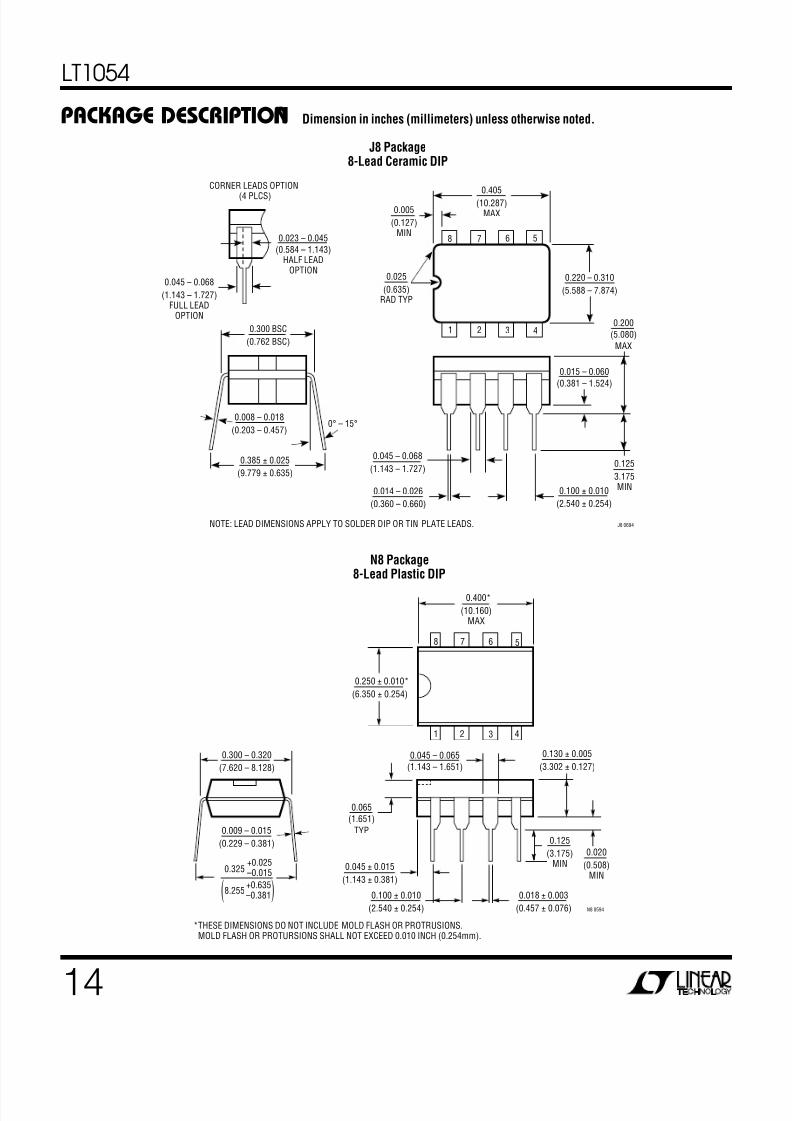
Dimension in inches (millimeters) unless otherwise noted.
H Package8-Lead TO-5 Metal Can
PACKAGE DESCRIPTION U
NOTE: LEAD DIAMETER IS UNCONTROLLED BETWEENTHE REFERENCE PLANE AND SEATING PLANE.
0.050(1.270)
MAX
0.016 – 0.021(0.406 – 0.533)
0.010 – 0.045
(0.254 – 1.143)
SEATINGPLANE
0.040
(1.016)MAX 0.165 – 0.185
(4.191 – 4.699)
GAUGEPLANE
REFERENCEPLANE
0.500 – 0.750
(12.700 – 19.050)
0.305 – 0.335
(7.747 – 8.509)
0.335 – 0.370(8.509 – 9.398)DIA
0.200 – 0.230
(5.080 – 5.842)BSC
0.027 – 0.045(0.686 – 1.143)
0.027 – 0.034(0.686 – 0.864)
0.110 – 0.160(2.794 – 4.064)
INSULATINGSTANDOFF
45°TYP
H8(5) 0592
Positive Doubler with Regulation(5V to 8V Converter)
2µF10µF
0.03µF
VIN = 5V
50k
1N5817
1N5817
LT1054 • TA13
+
+
–
+
10k
10k
10k
5.5k
2.5k
0.1µF
5V
LT1006
100µF
VOUT8V
+
LT1054
FB/SHDN
CAP+
GND
CAP–
V+
OSC
VREF
VOUT
Negative Doubler with Regulator
10µF
2µF
VIN3.5V TO 15V
100µFR21M
1N4001 1N4001
LT1054 • TA14
+
10µF +
+
+
100µF +
0.002µF
–VOUT
VIN = 3.5V TO 15VVOUT(MAX) ≈ 2VIN + (VL + 2VDIODE)VL = LT1054 VOLTAGE LOSS
, REFER TO FIGURE 5R2
R1
= =+ 1|VOUT|
) )VREF2 – 40mV
) )+ 1
|VOUT|
1.21V
LT1054
FB/SHDN
CAP+
GND
CAP–
V+
OSC
VREF
VOUT
THE TYPICAL APPLICATIONS CIRCUITS WERE VERIFIED USING THE STANDARD LT1054. FOR S8 APPLICATIONSASSISTANCE IN ANY OF THE UNUSUAL APPLICATIONS CIRCUITS PLEASE CONSULT THE FACTORY
8/3/2019 lt1054
http://slidepdf.com/reader/full/lt1054 14/1614
LT1054
Dimension in inches (millimeters) unless otherwise noted.PACKAGE DESCRIPTION U
J8 Package8-Lead Ceramic DIP
N8 Package8-Lead Plastic DIP
J8 0694
0.014 – 0.026
(0.360 – 0.660)
0.200
(5.080)
MAX
0.015 – 0.060
(0.381 – 1.524)
0.125
3.175MIN0.100 ± 0.010
(2.540 ± 0.254)
0.300 BSC
(0.762 BSC)
0.008 – 0.018
(0.203 – 0.457)0° – 15°
0.385 ± 0.025
(9.779 ± 0.635)
0.005
(0.127)MIN
0.405
(10.287)MAX
0.220 – 0.310
(5.588 – 7.874)
1 2 3 4
8 7 6 5
0.025
(0.635)RAD TYP
0.045 – 0.068
(1.143 – 1.727)FULL LEAD
OPTION
0.023 – 0.045
(0.584 – 1.143)HALF LEAD
OPTION
CORNER LEADS OPTION
(4 PLCS)
0.045 – 0.068
(1.143 – 1.727)
NOTE: LEAD DIMENSIONS APPLY TO SOLDER DIP OR TIN PLATE LEADS.
N8 0594
0.045 ± 0.015
(1.143 ± 0.381)
0.100 ± 0.010
(2.540 ± 0.254)
0.065(1.651)
TYP
0.045 – 0.065(1.143 – 1.651)
0.130 ± 0.005
(3.302 ± 0.127)
0.020
(0.508)MIN
0.018 ± 0.003
(0.457 ± 0.076)
0.125
(3.175)MIN
1 2 3 4
8 7 6 5
0.250 ± 0.010*
(6.350 ± 0.254)
0.400*
(10.160)MAX
0.009 – 0.015
(0.229 – 0.381)
0.300 – 0.320
(7.620 – 8.128)
0.325+0.025–0.015
+0.635–0.381
8.255( )
*THESE DIMENSIONS DO NOT INCLUDE MOLD FLASH OR PROTRUSIONS.MOLD FLASH OR PROTURSIONS SHALL NOT EXCEED 0.010 INCH (0.254mm).

8/3/2019 lt1054
http://slidepdf.com/reader/full/lt1054 15/1615
LT1054
Dimension in inches (millimeters) unless otherwise noted.PACKAGE DESCRIPTION U
Information furnished by Linear Technology Corporation is believed to be accurate and reliable.
However, no responsibility is assumed for its use. Linear Technology Corporation makes no represen-tation that the interconnection of its circuits as described herein will not infringe on existing patent rights.
S8 Package8-Lead Ceramic DIP
SOL16 0392
NOTE:1. PIN 1 IDENT, NOTCH ON TOP AND CAVITIES ON THE BOTTOM OF PACKAGES ARE THE MANUFACTURING OPTIONS.
THE PART MAY BE SUPPLIED WITH OR WITHOUT ANY OF THE OPTIONS.
NOTE 1
0.398 – 0.413(10.109 – 10.490)
(NOTE 2)
16 15 14 13 12 11 10 9
1 2 3 4 5 6 7 8
0.394 – 0.419(10.007 – 10.643)
0.037 – 0.045(0.940 – 1.143)
0.004 – 0.012(0.102 – 0.305)
0.093 – 0.104(2.362 – 2.642)
0.050(1.270)
TYP0.014 – 0.019
(0.356 – 0.482)TYP
0° – 8° TYP
NOTE 1
0.005(0.127)
RAD MIN
0.009 – 0.013(0.229 – 0.330)
0.016 – 0.050(0.406 – 1.270)
0.291 – 0.299(7.391 – 7.595)
(NOTE 2)
× 45°0.010 – 0.029(0.254 – 0.737)
2. THESE DIMENSIONS DO NOT INCLUDE MOLD FLASH OR PROTRUSIONS.MOLD FLASH OR PROTRUSIONS SHALL NOT EXCEED 0.006 INCH (0.15mm).
S Package16-Lead Plastic SOL
0.016 – 0.0500.406 – 1.270
0.010 – 0.020
(0.254 – 0.508)× 45°
0°– 8° TYP0.008 – 0.010
(0.203 – 0.254)
SO8 0294
0.053 – 0.069(1.346 – 1.752)
0.014 – 0.019
(0.355 – 0.483)
0.004 – 0.010(0.101 – 0.254)
0.050(1.270)
BSC
1 2 3 4
0.150 – 0.157*(3.810 – 3.988)
8 7 6 5
0.189 – 0.197*
(4.801 – 5.004)
0.228 – 0.244
(5.791 – 6.197)
*THESE DIMENSIONS DO NOT INCLUDE MOLD FLASH OR PROTRUSIONS.
MOLD FLASH OR PROTRUSIONS SHALL NOT EXCEED 0.006 INCH (0.15mm).

8/3/2019 lt1054
http://slidepdf.com/reader/full/lt1054 16/16
LT1054
LT/GP 0395 5K REV C • PRINTED IN USALinear Technology Corporation
TAIWAN
Linear Technology CorporationRm. 801, No. 46, Sec. 2
Chung Shan N. Rd.Taipei, Taiwan, R.O.C.
Phone: 886-2-521-7575
FAX: 886-2-562-2285
UNITED KINGDOMLinear Technology (UK) Ltd.
The Coliseum, Riverside Way
Camberley, Surrey GU15 3YLUnited Kingdom
Phone: 44-1276-677676FAX: 44-1276-64851
NORTHEAST REGION
Linear Technology Corporation
3220 Tillman Drive, Suite 120Bensalem, PA 19020
Phone: (215) 638-9667FAX: (215) 638-9764
Linear Technology Corporation266 Lowell St., Suite B-8
Wilmington, MA 01887Phone: (508) 658-3881
FAX: (508) 658-2701
U.S. Area Sales Offices
SOUTHEAST REGION
Linear Technology Corporation17000 Dallas Parkway
Suite 219
Dallas, TX 75248Phone: (214) 733-3071
FAX: (214) 380-5138
CENTRAL REGIONLinear Technology Corporation
Chesapeake Square
229 Mitchell Court, Suite A-25Addison, IL 60101
Phone: (708) 620-6910FAX: (708) 620-6977
SOUTHWEST REGION
Linear Technology Corporation
22141 Ventura Blvd.Suite 206
Woodland Hills, CA 91364Phone: (818) 703-0835
FAX: (818) 703-0517
NORTHWEST REGION
Linear Technology Corporation782 Sycamore Dr.
Milpitas, CA 95035Phone: (408) 428-2050
FAX: (408) 432-6331
FRANCE
Linear Technology S.A.R.L.
Immeuble "Le Quartz"58 Chemin de la Justice
92290 Chatenay MalabryFrance
Phone: 33-1-41079555
FAX: 33-1-46314613
GERMANYLinear Technology GmbH
Untere Hauptstr. 9
D-85386 EchingGermany
Phone: 49-89-3197410FAX: 49-89-3194821
JAPAN
Linear Technology KK
5F NAO Bldg.1-14 Shin-Ogawa-cho Shinjuku-ku
Tokyo, 162 JapanPhone: 81-3-3267-7891
FAX: 81-3-3267-8510
KOREA
Linear Technology Korea BranchNamsong Building, #505
Itaewon-Dong 260-199
Yongsan-Ku, SeoulKorea
Phone: 82-2-792-1617FAX: 82-2-792-1619
SINGAPORE
Linear Technology Pte. Ltd.
507 Yishun Industrial Park ASingapore 2776
Phone: 65-753-2692FAX: 65-754-4113
World Headquarters
Linear Technology Corporation1630 McCarthy Blvd.
Milpitas, CA 95035-7487
Phone: (408) 432-1900FAX: (408) 434-0507
0295
International Sales Offices
