LSI/CSI LS7366R · LSI/CSI . U. L ® LSI Computer Systems, Inc. 1235 Walt Whitman Road, Melville,...
17
LSI/CSI U L ® LSI Computer Systems, Inc. 1235 Walt Whitman Road, Melville, NY 11747 (631) 271-0400 FAX (631) 271-0405 A3800 32-BIT QUADRATURE COUNTER WITH SERIAL INTERFACE GENERAL FEATURES: • Operating voltage: 3V to 5.5V (VDD - VSS) • 5V count frequency: 40MHz • 3V count frequency: 20MHz • 32-bit counter (CNTR). • 32-bit data register (DTR) and comparator. • 32-bit output register (OTR). • Two 8-bit mode registers (MDR0, MDR1) for programmable functional modes. • 8-bit instruction register (IR). • 8-bit status register (STR). • Latched Interrupt output on Carry or Borrow or Compare or Index. • Index driven counter load, output register load or counter reset. • Internal quadrature clock decoder and filter. • x1, x2 or x4 mode of quadrature counting. • Non-quadrature up/down counting. • Modulo-N, Non-recycle, Range-limit or Free-running modes of counting • 8-bit, 16-bit, 24-bit and 32-bit programmable configuration synchronous (SPI) serial interface • LS7366R (DIP), LS7366R-S (SOIC), LS7366R-TS (TSSOP) - See Figure 1 - SPI/MICROWIRE (Serial Peripheral Interface): • Standard 4-wire connection: MOSI, MISO, SS/ and SCK. • Slave mode only. GENERAL DESCRIPTION: LS7366R is a 32-bit CMOS counter, with direct interface for quadra- ture clocks from incremental encoders. It also interfaces with the index signals from incremental encoders to perform variety of marker functions. For communications with microprocessors or microcontrollers, it provides a 4-wire SPI/MICROWIRE bus.The four standard bus I/Os are SS/, SCK, MISO and MOSI. The data transfer between a micro- controller and a slave LS7366R is synchronous. The synchroniza- tion is done by the SCK clocks supplied by the microcontroller. Each transmission is organized in blocks of 1 to 5 bytes of data. A trans- mission cycle is intitiated by a high to low transition of the SS/ input. The first byte received in a transmission cycle is always an instruc- tion byte, whereas the second through the fifth bytes are always interpreted as data bytes. A transmission cycle is terminated with the low to high transition of the SS/ input. Received bytes are shifted in at the MOSI input, MSB first, with the leading edges (high transi- tion) of the SCK clocks. Output data are shifted out on the MISO output, MSB first, with the trailing edges (low transition) of the SCK clocks. 7366R-061814-1 June 2014 PIN ASSIGNMENT TOP VIEW LS7366R 14 13 12 11 10 9 8 1 2 3 4 5 6 7 V DD CNT_EN A B INDEX/ DFLAG/ LFLAG/ f CKO f CKi V SS SS/ SCK MISO MOSI FIGURE 1 Read and write commands cannot be combined. For example, when the device is shifting out read data on MISO output, it ignores the MOSI input, even though the SS/ input is active. SS/ must be terminated and reasserted before the device will accept a new command. The counter can be configured to operate as 1, 2, 3 or 4-byte counter. When configured as an n-byte counter, the CNTR, DTR and OTR are all config- ured as n-byte registers, where n = 1, 2, 3 or 4. The content of the instruction/data identity is automatically adjusted to match the n-byte configu- ration. For example, if the counter is configured as a 2-byte counter, the instruction “write to DTR” expects 2 data bytes following the instruction byte. If the counter is configured as a 3-byte counter, the same instruction will expect 3 bytes of data follow- ing the instruction byte. Following the transfer of the appropriate number of bytes any further attempt of data transfer is ignored until a new instruction cycle is started by switching the SS/ input to high and then low. The counter can be programmed to operate in a number of different modes, with the operating characteristics being written into the two mode registers MDR0 and MDR1. Hardware I/Os are provided for event driven operations, such as processor interrupt and index related functions.
Transcript of LSI/CSI LS7366R · LSI/CSI . U. L ® LSI Computer Systems, Inc. 1235 Walt Whitman Road, Melville,...

LSI/CSI UL
®
LSI Computer Systems, Inc. 1235 Walt Whitman Road, Melville, NY 11747 (631) 271-0400 FAX (631) 271-0405 A3800
32-BIT QUADRATURE COUNTER WITH SERIAL INTERFACE
GENERAL FEATURES:
• Operating voltage: 3V to 5.5V (VDD - VSS) • 5V count frequency: 40MHz • 3V count frequency: 20MHz • 32-bit counter (CNTR). • 32-bit data register (DTR) and comparator. • 32-bit output register (OTR). • Two 8-bit mode registers (MDR0, MDR1)
for programmable functional modes. • 8-bit instruction register (IR). • 8-bit status register (STR). • Latched Interrupt output on Carry or Borrow or Compare or Index. • Index driven counter load, output register load or counter reset. • Internal quadrature clock decoder and filter. • x1, x2 or x4 mode of quadrature counting. • Non-quadrature up/down counting. • Modulo-N, Non-recycle, Range-limit or
Free-running modes of counting • 8-bit, 16-bit, 24-bit and 32-bit programmable configuration
synchronous (SPI) serial interface • LS7366R (DIP), LS7366R-S (SOIC), LS7366R-TS (TSSOP)
- See Figure 1 -
SPI/MICROWIRE (Serial Peripheral Interface): • Standard 4-wire connection: MOSI, MISO, SS/ and SCK. • Slave mode only.
GENERAL DESCRIPTION:
LS7366R is a 32-bit CMOS counter, with direct interface for quadra- ture clocks from incremental encoders. It also interfaces with the index signals from incremental encoders to perform variety of marker functions.
For communications with microprocessors or microcontrollers, it provides a 4-wire SPI/MICROWIRE bus.The four standard bus I/Os are SS/, SCK, MISO and MOSI. The data transfer between a micro- controller and a slave LS7366R is synchronous. The synchroniza- tion is done by the SCK clocks supplied by the microcontroller. Each transmission is organized in blocks of 1 to 5 bytes of data. A trans- mission cycle is intitiated by a high to low transition of the SS/ input. The first byte received in a transmission cycle is always an instruc- tion byte, whereas the second through the fifth bytes are always interpreted as data bytes. A transmission cycle is terminated with the low to high transition of the SS/ input. Received bytes are shifted in at the MOSI input, MSB first, with the leading edges (high transi- tion) of the SCK clocks. Output data are shifted out on the MISO output, MSB first, with the trailing edges (low transition) of the SCK clocks.
7366R-061814-1
June 2014
PIN ASSIGNMENT
TOP VIEW
LS7366R
14
13
12
11
10
9
8
1
2
3
4
5
6
7
V DD
CNT_EN
A
B
INDEX/
DFLAG/
LFLAG/
fCKO
fCKi
V SS
SS/
SCK
MISO
MOSI
FIGURE 1
Read and write commands cannot be combined. For example, when the device is shifting out read data on MISO output, it ignores the MOSI input, even though the SS/ input is active. SS/ must be terminated and reasserted before the device will accept a new command. The counter can be configured to operate as 1, 2, 3 or 4-byte counter. When configured as an n-byte counter, the CNTR, DTR and OTR are all config- ured as n-byte registers, where n = 1, 2, 3 or 4. The content of the instruction/data identity is automatically adjusted to match the n-byte configu- ration. For example, if the counter is configured as a 2-byte counter, the instruction “write to DTR” expects 2 data bytes following the instruction byte. If the counter is configured as a 3-byte counter, the same instruction will expect 3 bytes of data follow- ing the instruction byte. Following the transfer of the appropriate number of bytes any further attempt of data transfer is ignored until a new instruction cycle is started by switching the SS/ input to high and then low. The counter can be programmed to operate in a number of different modes, with the operating characteristics being written into the two mode registers MDR0 and MDR1. Hardware I/Os are provided for event driven operations, such as processor interrupt and index related functions.

7366R-081507-2
I/O Pins:Following is a description of all the input/output pins.
A (Pin 12) B (Pin 11)Inputs. A and B quadrature clock outputs from incrementalencoders are directly applied to the A and B inputs of theLS7366R. These clocks are ideally 90 degrees out-of-phasesignals. A and B inputs are validated by on-chip digital filtersand then decoded for up/down direction and count clocks.In non-quadrature mode, A serves as the count input and Bserves as the direction input (B = high enables up count, B = low enables down count). In non-quadrature mode, the A and B inputs are not filtered internally, and are instan-taneous in nature.
INDEX/ (Pin 10)Input. The INDEX/ is a programmable input that can bedriven directly by the Index output of an incremental encod-er. It can be programmed via the MDR0 to function as oneof the following:LCNTR (load CNTR with data from DTR), RCNTR (resetCNTR), or LOTR (load OTR with data from CNTR).Alternatively, the INDEX input can be masked out for "nofunctionality".
In quadrature mode, the INDEX/ input can be configured tooperate in either synchronous or asynchronous mode. In thesynchronous mode the INDEX/ input is sampled with thesame filter clock used for sampling the A and the B inputsand must satisfy the phase relationship in which the INDEX/is in the active level of Logic 0 during a minimum of aquarter cycle of both A and B High or both A and B Low. Innon-quadrature mode, the INDEX/ input is unconditionallyset to the asynchronous mode. In the asynchronous mode,the INDEX/ input is not sampled and can be applied in anyphase relationship with respect to A and B.
fCKi (Pin 2), fCK0 (Pin 1)Input, Output. A crystal connected between these 2 pinsgenerates the basic clock for filtering the A, B and INDEX/inputs in the quadrature count mode. Instead of a crystal thefCKi input may also be driven by an external clock.
The frequency at the fCKi input is either divided by 2(if MDR0 <B7> = 1) or divided by 1 (if MDR0 <B7> = 0) forthe filter circuit. For proper filtering of the A, B and the Index/inputs the following condition must be satisfied: ff ≥ 4fQAWhere ff is the internal filter clock frequency derived from thefCKi in accordance with the status of MDR0 <B7> and fQA isthe maximum frequency of Clock A in quadrature mode. Innon-quadrature count mode, fCKi is not used and should betied off to any stable logic state.
SS/ (Pin 4)A high to low transition at the SS/ (Slave Select) inputselects the LS7366R for serial bi-directional data transfer; alow to high transition disables serial data transfer and bringsthe MISO output to high impedance state. This allows for theaccommodation of multiple slave units on the serial I/O.
CNT_EN (Pin 13)Input. Counting is enabled when CNT_EN input is high; countingis disabled when this input is low. There is an internal pull-upresistor on this input.
LFLAG/ (Pin 8), DFLAG/ (Pin 9)Outputs. LFLAG/ and DFLAG/ are programmable outputs to flagthe occurences of Carry (counter overflow), Borrow (counterunderflow), Compare (CNTR = DTR) and INDEX. The LFLAG/ isan open drain latched output. In contrast, the DFLAG/ is a push-pull instantaneous output. The LFLAG/ can be wired in multi-slave configuration, forming a single processor interrupt line.When active LFLAG/ switches to logic 0 and can be restored tothe high impedence state only by clearing the status register,STR. In contrast, the DFLAG/ dynamically switches low withoccurences of Carry, Barrow, Compare and INDEX conditions.
The configuration of LFLAG/ and DFLAG/ are made through thecontrol register MDR1.
MOSI (RXD) (Pin 7)Input. Serial output data from the host processor is shifted intothe LS7366R at this input.
MISO (TXD) (Pin 6)Output. Serial output data from the LS7366R is shifted out onthe MISO (Master In Slave Out) pin. The MISO output goes intohigh impedance state when SS/ input is at logic high, providingmultiple slave-unit serial outputs to be wire-ORed.
SCK (Pin 5)Input. The SCK input serves as the shift clock input for transmit-ting data in and out of LS7366R on the MOSI and the MISOpins, respectively. Since the LS7366R can operate only in theslave mode, the SCK signal is provided by the host processoras a means for synchronizing the serial transmission betweenitself and the slave LS7366R.
REGISTERS:The following is a list of LS7366R internal registers:
Upon power-up the registers DTR, CNTR, STR, MDR0 andMDR1 are reset to zero.
DTR. The DTR is a software configurable 8, 16, 24 or 32-bitinput data register which can be written into directly from MOSI,the serial input. The DTR data can be transferred into the 32-bitcounter (CNTR) under program control or by hardware indexsignal. The DTR can be cleared to zero by software control. Incertain count modes, such as modulo-n and range-limit, DTRholds the data for "n" and the count range, respectively. Incompare operations, whereby compare flag is set, the DTR iscompared with the CNTR.
The information included herein is believed to beaccurate and reliable. However, LSI Computer Systems,Inc. assumes no responsibilities for inaccuracies, nor forany infringements of patent rights of others which mayresult from its use.
STR. The STR is an 8-bit status register which stores count related status information.
CY BW CMP IDX CEN PLS U/D S 7 6 5 4 3 2 1 0
7366R-102708-3
IR. The IR is an 8-bit register that fetches instruction bytes fromthe received data stream and executes them to perform suchfunctions as setting up the operating mode for the chip (load theMDR) and data transfer among the various registers.
B7 B6 B5 B4 B3 B2 B1 B0
B2 B1 B0 = XXX (Don’t care) B5 B4 B3 = 000: Select none
= 001: Select MDR0 = 010: Select MDR1= 011: Select DTR= 100: Select CNTR= 101: Select OTR = 110: Select STR= 111: Select none
B7 B6 = 00: CLR register= 01: RD register= 10: WR register= 11: LOAD register
The actions of the four functions, CLR, RD, WR and LOAD are elaborated in Table 1.
TABLE 1Number of Bytes OP Code Register Operation
MDR0 Clear MDR0 to zeroMDR1 Clear MDR1 to zero
1 CLR DTR NoneCNTR Clear CNTR to zeroOTR NoneSTR Clear STR to zero
MDR0 Output MDR0 serially on TXD (MISO)MDR1 Output MDR1 serially on TXD (MISO)
2 to 5 RD DTR NoneCNTR Transfer CNTR to OTR, then output OTR serially
on TXD (MISO)OTR Output OTR serially on TXD (MISO)STR Output STR serially on TXD (MISO)
MDR0 Write serial data at RXD (MOSI) into MDR0MDR1 Write serial data at RXD (MOSI) into MDR1
2 to 5 WR DTR Write serial data at RXD (MOSI) into DTRCNTR NoneOTR NoneSTR None
MDR0 NoneMDR1 None
1 LOAD DTR NoneCNTR Transfer DTR to CNTR in “parallel”OTR Transfer CNTR to OTR in “parallel”
CNTR. The CNTR is a software configurable 8, 16, 24 or 32-bit up/down counter which counts the up/down pulses resulting from the quadrature clocks applied at the A and B inputs, or alternatively, in non-quadrature mode, pulses applied at the A input. By means of IR intructions the CNTR can be cleared, loaded from the DTR or in turn, can be transferred into the OTR.
OTR. The OTR is a software configuration 8, 16, 24 or 32-bit register which can be read back on the MISO output. Since instantaneous CNTR value is often needed to be read while the CNTR continues to count, the OTR serves as a convenient dump site for instantaneous CNTR data which can then be read without interfering with the counting process.
CY: Carry (CNTR overflow) latchBW: Borrow (CNTR underflow) latch
CMP: Compare (CNTR = DTR) latch IDX: Index latch
CEN: Count enable status: 0: counting disabled, 1: counting enabled
PLS: Power loss indicator latch; set upon power up U/D: Count direction indicator: 0: count down, 1: count up S: Sign bit. 1: negative, 0: positive

7366R-041906-4
ABSOLUTE MAXIMUM RATINGS:(All voltages referenced to Vss)
Parameter Symbol Values UnitDC Supply Voltage VDD +7.0 VInput Voltage VIN Vss - 0.3 to VDD + 0.3 VOperating Temperature TA -25 to +80 oCStorage Temperature TSTG 65 to +150 oC
MDR1. The MDR1 (Mode Register 1) is an 8-bit read/write register which is appended to MDR0 for additional modes. Upon power-up MDR1 is cleared to zero.
B7 B6 B5 B4 B3 B2 B1 B0
B1 B0 = 00: 4-byte counter mode = 01: 3-byte counter mode
= 10: 2-byte counter mode. = 11: 1-byte counter mode
B2 = 0: Enable counting = 1: Disable counting
B3 = : not used B4 = 0: NOP
= 1: FLAG on IDX (B4 of STR) B5 = 0: NOP
= 1: FLAG on CMP (B5 of STR) B6 = 0: NOP
= 1: FLAG on BW (B6 of STR) B7 = 0: NOP
= 1: FLAG on CY (B7 of STR)
MDR0. The MDR0 (Mode Register 0) is an 8-bit read/write register that sets up the operating mode for the LS7366R. The MDR0 iswritten into by executing the "write-to-MDR0" instruction via the instruction register. Upon power up MDR0 is cleared to zero. Thefollowing is a breakdown of the MDR bits:
B7 B6 B5 B4 B3 B2 B1 B0
B1 B0 = 00: non-quadrature count mode. (A = clock, B = direction). = 01: x1 quadrature count mode (one count per quadrature cycle).
= 10: x2 quadrature count mode (two counts per quadrature cycle). = 11: x4 quadrature count mode (four counts per quadrature cycle).
B3 B2 = 00: free-running count mode. = 01: single-cycle count mode (counter disabled with carry or borrow, re-enabled with reset or load). = 10: range-limit count mode (up and down count-ranges are limited between DTR and zero,
respectively; counting freezes at these limits but resumes when direction reverses). = 11: modulo-n count mode (input count clock frequency is divided by a factor of (n+1),
where n = DTR, in both up and down directions).
B5 B4 = 00: disable index. = 01: configure index as the "load CNTR" input (transfers DTR to CNTR). = 10: configure index as the "reset CNTR" input (clears CNTR to 0). = 11: configure index as the "load OTR" input (transfers CNTR to OTR).
B6 = 0: Asynchronous Index = 1: Synchronous Index (overridden in non-quadrature mode) B7 = 0: Filter clock division factor = 1 = 1: Filter clock division factor = 2
NOTE: Applicable to bothLFLAG/ and DFLAG/

DC Electrical Characteristics. (TA = -25˚C to +85°C) Parameter Symbol Min. TYP Max. Unit RemarksSupply Voltage VDD 3.0 - 5.5 V -Supply Current IDD 300 400 450 µA VDD = 3.0V
IDD 700 800 950 µA VDD = 5.0VInput VoltagesfCKi, Logic high VCH 2.3 - - V VDD = 3.0V
VCH 3.7 - - V VDD = 5.0VfCKi, Logic Low VCL - - 0.7 V VDD = 3.0V
VCL - - 1.3 V VDD = 5.0All other inputs, Logic High VAH 2.1 - V VDD = 3.0V
VAH 3.5 - V VDD = 5.0V
All other inputs, Logic Low VAL - - 0.5 V VDD = 3.0VVAL - - 1.0 V VDD = 5.0V
Input Currents:CNT_EN Low IIEL - 3.0 5.0 µA VAL = 0.7V, VDD = 3.0V
IIEL - 10.0 15.0 µA VAL = 1.2V, VDD = 5.0V
CNT_EN High IIEH - 1.0 3.0 µA VAH = 1.9V, VDD = 3.0VIIEH - 6.0 9.0 µA VAH = 3.2V, VDD = 5.0V
All other inputs, High or Low - - 0 0 µA -
Output Currents:LFLAG, DFLAG Sink IOFL -1.3 -2.0 - mA VOUT = 0.5V, VDD = 3.0V IOFL -3.2 -4.0 - mA VOUT = 0.5V, VDD = 5.0VLFLAG Source - 0 0 - mA Open Drain OutputDFLAG Source IOFH 1.0 1.8 - mA VOUT = 2.5V, VDD = 3.0V
IOFH 2.8 3.6 - mA VOUT = 4.5V, VDD = 5.0V
fCKO Sink IOCL -1.3 -2.0 - mA VOUT = 0.5V, VDD = 3.0V IOCL -3.2 -4.0 - mA VOUT = 0.5V, VDD = 5.0VfCKO Source IOCH 1.3 2.0 - mA VOUT = 2.5V, VDD = 3.0V IOCH 3.2 4.0 - mA VOUT = 4.5V, VDD = 5.0VTXD/MISO: Sink IOML -1.5 -2.4 - mA VOUT = 0.5V, VDD = 3.0V IOML -3.8 -4.8 - mA VOUT = 0.5V, VDD = 5.0V
Source IOMH 1.5 2.4 - mA VOUT = 2.5V, VDD = 3.0V IOMH 3.8 4.8 - mA VOUT = 4.5V, VDD = 5.0V
7366R-091109-5
Transient Characteristics. (TA = -25˚C to +85˚C, VDD = 5V ± 10%)
Parameter Symbol Min. Value Max.Value Unit Remarks(See Fig. 2) SCK High Pulse Width tCH 100 - ns -SCK Low Pulse Width tCL 100 - ns -SS/ Set Up Time tCSL 100 - ns -SS/ Hold Time tCSH 100 - ns -Inter Command SS/ high tCSI 100 - ns -
Quadrature Mode(See Fig. 5, 7 & 8 )fCKI High Pulse Width t1 12 - ns -fCKI Pulse Width t2 12 - ns -fCKI Frequency fFCK - 40 MHz -Effective Filter Clock fF Period t3 25 - ns t3 = t1+t2, MDR0 <7> = 0
t3 50 - ns t3 = 2(t1+t2), MDR0 <7> = 1Effective Filter Clock fF frequency fF - 40 MHz fF = 1/ t3Quadrature Separation t4 26 - ns t4 > t3Quadrature Clock Pulse Width t5 52 - ns t5 ≥ 2t3Quadrature Clock frequency fQA, fQB - 9.6 MHz fQA = fQB < 1/4t3Quadrature Clock to Count Delay tQ1 4t3 5t3 - -x1 / x2 / x4 Count Clock Pulse Width tQ2 12 - ns tQ2 = (t3)/2Index Input Pulse Width tid 32 - ns tid > t4Index Set Up Time tis - 5 ns -Index Hold Time tih - 5 ns -Quadrature clock to tfl 4.5t3 5.5t3 ns -DFLAG/ or LFLAG/ delayDFLAG/ output width tfw 26 - ns tfw = t4

Parameter Symbol Min. Value Max.Value Unit Remarks
Non-Quadrature Mode(See Fig. 6 & 9) Clock A - High Pulse Width t6 12 - ns -Clock A - Low Pulse Width t7 12 - ns -Direction Input B Set-up Time t8S 12 - ns -Direction Input B Hold Time t8H 10 - ns -CNT_EN Set-up Time t9S 12 - ns -CNT_EN Hold Time t9H 12 - ns -Clock Frequency (non-Mod-N) fA - 40 MHz fA = (1/(t6 + t7))Clock to DFLAG/ or t10 20 - ns -LFLAG/ delayDFLAG/ output width t11 12 - ns t10 = t7
Transient Characteristics. (TA = -25˚C to +85˚C, VDD = 3.3V ± 10%)
Parameter Symbol Min. Value Max.Value Unit Remarks(See Fig. 2) SCK High Pulse Width tCH 120 - ns -SCK Low Pulse Width tCL 120 - ns -SS/ Set Up Time tCSL 120 - ns -SS/ Hold Time tCSH 120 - ns -Inter Command SS/ high tCSI 120 - ns -
Quadrature Mode(See Fig. 5, 7 & 8)fCKI High Pulse Width t1 24 - ns -fCKI Pulse Width t2 24 - ns -fCKI Frequency fFCK - 20 MHz -Effective Filter Clock fF Period t3 50 - ns t3 = t1+t2, MDR0 <7> = 0
t3 100 - ns t3 = 2(t1+t2), MDR0 <7> = 1Effective Filter Clock fF frequency fF - 20 MHz fF = 1/ t3Quadrature Separation t4 52 - ns t4 > t3Quadrature Clock Pulse Width t5 105 - ns t5 ≥ 2t3Quadrature Clock frequency fQA, fQB - 4.5 MHz fQA = fQB < 1/4t3Quadrature Clock to Count Delay tQ1 4t3 5t3 - -x1/x2/x4 Count Clock Pulse Width tQ2 25 - ns tQ2 = (t3)/2Index Input Pulse Width tid 60 - ns tid > t4Index Set Up Time tis - 10 ns -Index Hold Time tih - 10 ns -Quadrature clock to tfl 4.5t3 5.5t3 ns -DFLAG/ or LFLAG/ delayDFLAG/ output width tfw 52 - ns tfw = t4
Non-Quadrature Mode(See Fig. 6 & 9) Clock A - High Pulse Width t6 24 - ns -Clock A - Low Pulse Width t7 24 - ns -Direction Input B Set-up Time t8S 24 - ns -Direction Input B Hold Time t8H 24 - ns -Clock Frequency (non-Mod-N) fA - 20 MHz fA = (1/(t6 + t7))Clock to DFLAG/or t9 40 - ns -LFLAG/ delayDFLAG/ output width t10 24 - ns t10 = t7
7366R-061814-6
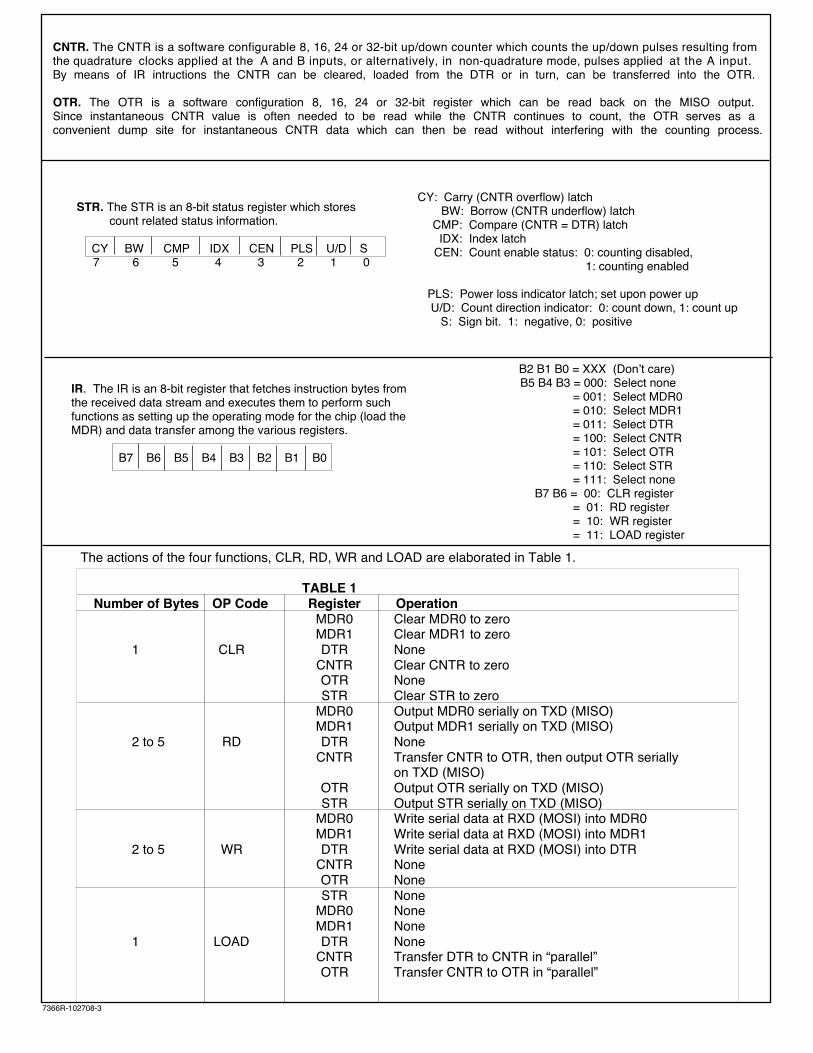
Note 1. The SPI port of the host MCU must be set up as follows:
1. SPI master mode. 2. SCK idle state = low
3. Clock edge for MOSI data shift = high to low 4. Clock edge for input data (MISO) sample by the Processor = low to high (or bit middle)
Note 2. To conform with the multibyte transmission protocol of LS7366R, the SS/ output port of the MCU may require direct manipulation by the application program.
FIGURE 2. SPI TIMINGS
7366R-041906-7
tCSH
tCL tCH
tCSL
MSB
LSB
SS/
SCK
MOSI
MISOHIGH IMPEDANCE
( )
( )
( )
( )
( )
( )
( )
( )

D7 D6 D5 D4 D3
D3
D2 D1 D0
D2D6 D5D7 D4 X X X RANDOM DATAX X X D1 D0 X
SS/
SCK
MOSI
MISO
BIT # 7 6 5 4 3 2 1 0 7 6 5 4 3 2 1 0 7 6 5 4 3 2 1 0
START OF NEW COMMAND
RD MDR1DATAWR MDR1
tCSL
BIT # 7 6 5 4 3 2 1 0
tCH tCL
TRI-STATE
D7 D6 D5 D4 D3D3 D2 D1 D0D2D6 D5D7 D4
XXXX X X
D1 D0
SS/
SCK
MOSI
MISO
BIT # 7 6 5 4 3 2 1 0
7 6 5 4 3 2 1 0
RD CNTR
tCSI
BIT # 7 6 5 4 3 2 1 0
BYTE 1 BYTE 0
CLR STR
RANDOM DATA
7 6 5 4 3 2 1 0
TRI-STATE
NOTE: Write to MDR1 followed by Read from MDR1 operation
7366R-120407-8
FIGURE 3. WR MDR1 - RD MDR1
FIGURE 4. RD CNTR - CLR STR
FIGURE 5. fCKI, A, B and INDEX
Note 1. Synchronous index coincident with both A and B high.Note 2. Synchronous index coincident with both A and B low.. Note 3. fF is the internal effective filter clock.
NOTE: Read CNTR (in 2-byte configuration) followed by CLR STR operation.
fCKi
t1 t2
ff (Note 3)(MDR0 <7> = 0)
ff (Note 3)(MDR0 <7> = 1)
A
B
INDEX/
t3
t3
t5 t5
t4 t4 t4 t4
Note 1 Note 2tid
tistih
tis tih

7366-081507-9
UP DOWN
A
B
X4_CLK
X2_CLK
X1_CLK
(see note)
(see note)
(see note)
tQ1
tQ2
Note: x1, x2, and x4 CLKs are internal up/down clocks derived from filtered and decoded quadrature clocks.
FIGURE 7. A/B QUADRATURE CLOCKS vs INTERNAL COUNT CLOCKS
Note: CNTR values are indicated in 3-byte mode
FIGURE 8. QUADRATURE CLOCKS vs FLAG OUTPUTS
FIGURE 6. COUNT (A) AND DIRECTION (B) INPUTS IN NON-QUADRATURE MODE
UP DOWN
A
B
X4_CLK
tfl
CNTR
DFLG/
LFLG/
tfl
CY CMP BW
FFFFFC FFFFFD FFFFFE FFFFFF FFFFFF FFFFFE FFFFFD000000 000001000002000001 000000
(SHOWN WITH DTR = 000OO1)
tfw
DOWN UP DOWN
t6 t7 t8s t8H
B
A
t9s
CNT_EN
t9H

7366R-050106-10
NOTE: CNTR values are indicated in 2-byte mode
FIGURE 9. SINGLE-CYCLE, NON-QUADRATURE
NOTE: CNTR values are indicated in 1-byte mode
FIGURE 10. MODULO-N, NON-QUADRATURE
NOTE: CNTR values are indicated in 1-byte mode
FIGURE 11. RANGE-LIMIT, NON-QUADRATURE
INDX/
DFLG/
CNTR
A
B
FFFFFFC FFFFFFD FFFFFFE FFFFFFF 2 1 0 FFFFFFF
CY
t9 t10
t11CNTR DISABLED CNTR DISABLED
(Shown with DTR = 2)
CNTR ENABLED
(LOAD CNTR)
UP DOWN
DFLAG/
CNTR
A
B
000000 000002 000001 000000
CMP
(Shown with DTR = 3)
BW
UP DOWN
000001 000002 000003 000003000000 000001 000002 000001
DFLAG/
CNTR
A
B
000003 000002 000001
CMP
(Shown with DTR = 3)
UP DOWN
000000 000001 000002 000000
BW BWBWCMP CMP CMP

7366R-041906-11
FIGURE 12. LS7366R BLOCK DIAGRAM
CLOCKCONTROL
IO DATACONTROL
FILTER
MUX
MODECONTROL
IO SHIFTREG
÷2
FLAGMASK STR
MDR1
MDR0
OTR
CNTR
DTR(32)
I R
LOAD CLR RDWR
CLRRD
FLAGS
WR
POR
EN_MDR1
EN_OTR
POR
EN_DTR
(32)
(32)
(8)
(8)
(8)
(5)
EN_CNTR CMPR
FLAGLOGIC
SCK
RXD/MOSI
SS/
A
B
INDEX/
fCKi
fCKO
V DD
V SS
POR GEN
POR
FLAGS
LFLAG/
TXD/MIS0
(8)
MDR0<7>
(V-)
(V+)
SPI_XMIT/
CNT_EN
V+
V+
(8)
EN_STR
EN_DTREN_CNTREN_OTR
EN_MDR0
EN_MDR1
EN_STR
(8)
6 BUFFER
LOAD
8
5
7
4
12
11
10
2
1
13
14
3
LOAD
EN_MDR0
BUFFER DFLAG/9

7366R-060112-12
FIGURE 14. PIC18C TO LS7366R
LS7366R
MISO
MOSI
SCK
SS/
PIC18CXXX
RC3/SCK
RC4/SDI
RC5/SDO
RA5 4
5
6
7
LS7366R
1M 30MHz
*Cm
*Cm
fCKI
fCKO
FIGURE 13. GENERAL I/O CONNECTIONS
ENCODER
INDEX/
A
B
1
2
10
12
11
Vss
SS/
SCK
INT/
RXD
TXD
SCK
SS/
GND
MOSI
MISO
LFLAG/ 8
6
7
5
4
+V
+V
+V
VDD V DD
MCU
3
*NOTE: Cm is chosen according to the following equations:
Cm = 2(C L - C P) - 10pF, whereC L = manufacturer's specified crystal load capacitance.
C P = PCB parasitic capacitance seen by the crystal.
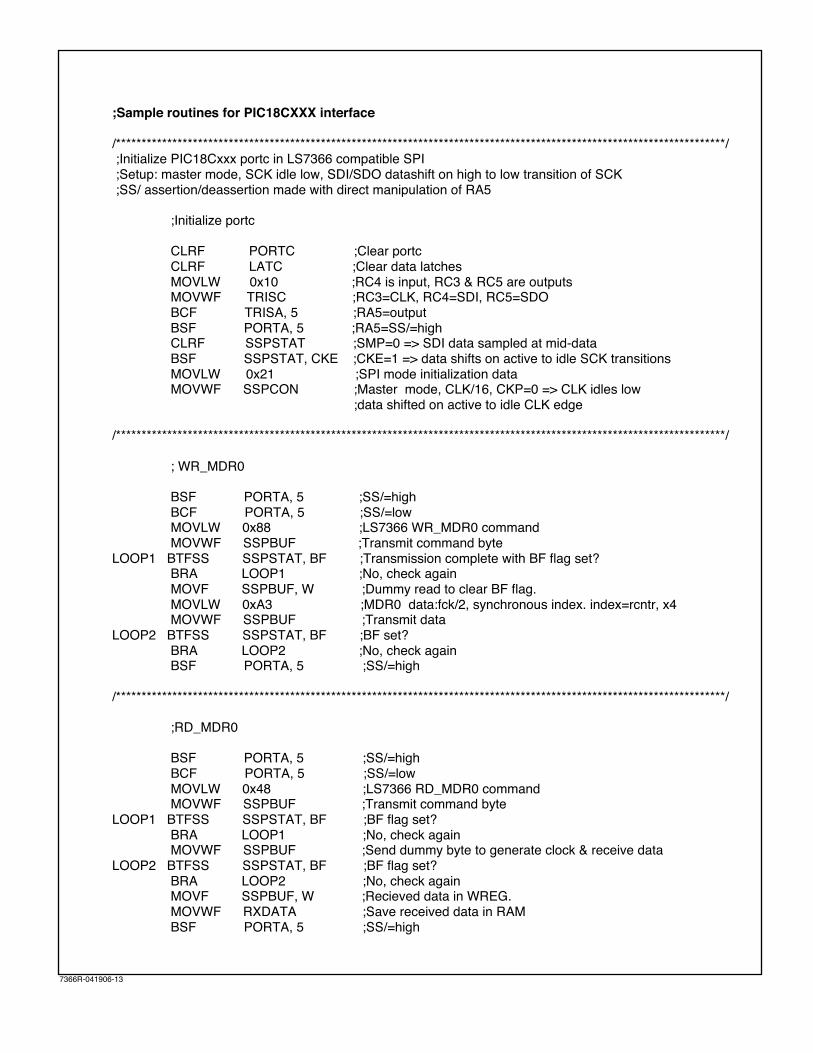
;Sample routines for PIC18CXXX interface
/***********************************************************************************************************************/ ;Initialize PIC18Cxxx portc in LS7366 compatible SPI ;Setup: master mode, SCK idle low, SDI/SDO datashift on high to low transition of SCK ;SS/ assertion/deassertion made with direct manipulation of RA5 ;Initialize portc
CLRF PORTC ;Clear portc CLRF LATC ;Clear data latches MOVLW 0x10 ;RC4 is input, RC3 & RC5 are outputs MOVWF TRISC ;RC3=CLK, RC4=SDI, RC5=SDO BCF TRISA, 5 ;RA5=output BSF PORTA, 5 ;RA5=SS/=high CLRF SSPSTAT ;SMP=0 => SDI data sampled at mid-data BSF SSPSTAT, CKE ;CKE=1 => data shifts on active to idle SCK transitions MOVLW 0x21 ;SPI mode initialization data MOVWF SSPCON ;Master mode, CLK/16, CKP=0 => CLK idles low ;data shifted on active to idle CLK edge
/***********************************************************************************************************************/ ; WR_MDR0 BSF PORTA, 5 ;SS/=high BCF PORTA, 5 ;SS/=low MOVLW 0x88 ;LS7366 WR_MDR0 command MOVWF SSPBUF ;Transmit command byteLOOP1 BTFSS SSPSTAT, BF ;Transmission complete with BF flag set? BRA LOOP1 ;No, check again MOVF SSPBUF, W ;Dummy read to clear BF flag. MOVLW 0xA3 ;MDR0 data:fck/2, synchronous index. index=rcntr, x4 MOVWF SSPBUF ;Transmit dataLOOP2 BTFSS SSPSTAT, BF ;BF set? BRA LOOP2 ;No, check again BSF PORTA, 5 ;SS/=high
/***********************************************************************************************************************/
;RD_MDR0 BSF PORTA, 5 ;SS/=high BCF PORTA, 5 ;SS/=low MOVLW 0x48 ;LS7366 RD_MDR0 command MOVWF SSPBUF ;Transmit command byteLOOP1 BTFSS SSPSTAT, BF ;BF flag set? BRA LOOP1 ;No, check again MOVWF SSPBUF ;Send dummy byte to generate clock & receive dataLOOP2 BTFSS SSPSTAT, BF ;BF flag set? BRA LOOP2 ;No, check again MOVF SSPBUF, W ;Recieved data in WREG. MOVWF RXDATA ;Save received data in RAM BSF PORTA, 5 ;SS/=high
7366R-041906-13

µC
MOSI
MISO
SCK
Pn<0:3>SS/<0:3>
MO
SI
MIS
O
SCK
MOSI
MISO
SCK
SS/
MO
SI
MIS
O
SCK
SS/<
0>
MO
SI
MIS
O
SCK
SS/
MO
SI
MIS
O
SCK
SS/<
1>
MO
SI
MIS
O
SCK
SS/
MO
SI
MIS
O
SCK
SS/<
2>
MO
SI
MIS
O
SCK
SS/
MO
SI
MIS
O
SCK
SS/<
3>
LS7366R LS7366R LS7366R LS7366R
fcki fcko fckifcki fcki
Fig 15. Multiple devices sharing common SPI bus.
7366R-080211-14
74HC14

//LS7366R to 90s8515 and ATmega32 SPI interface example
/********Add appropriate header files here**********/ /***MDR0 configuration data - the configuration byte is formed with*** ***single segments taken from each group and ORing all together.***/ //Count modes #define NQUAD 0x00 //non-quadrature mode #define QUADRX1 0x01 //X1 quadrature mode #define QUADRX2 0x02 //X2 quadrature mode #define QUADRX4 0x03 //X4 quadrature mode //Running modes #define FREE_RUN 0x00 #define SINGE_CYCLE 0x04 #define RANGE_LIMIT 0x08 #define MODULO_N 0x0C //Index modes #define DISABLE_INDX 0x00 //index_disabled #define INDX_LOADC 0x10 //index_load_CNTR #define INDX_RESETC 0x20 //index_rest_CNTR #define INDX_LOADO 0x30 //index_load_OL #define ASYNCH_INDX 0x00 //asynchronous index #define SYNCH_INDX 0x80 //synchronous index //Clock filter modes #define FILTER_1 0x00 //filter clock frequncy division factor 1 #define FILTER_2 0x80 //filter clock frequncy division factor 2 /* **MDR1 configuration data; any of these*** ***data segments can be ORed together***/ //Flag modes #define NO_FLAGS 0x00 //all flags disabled #define IDX_FLAG 0x10; //IDX flag #define CMP_FLAG 0x20; //CMP flag #define BW_FLAG 0x40; //BW flag #define CY_FLAG 0x80; //CY flag //1 to 4 bytes data-width #define BYTE_4 0x00; //four byte mode #define BYTE_3 0x01; //three byte mode #define BYTE_2 0x02; //two byte mode #define BYTE_1 0x03; //one byte mode //Enable/disable counter #define EN_CNTR 0x00; //counting enabled #define DIS_CNTR 0x04; //counting disabled /* LS7366R op-code list */ #define CLR_MDR0 0x08 #define CLR_MDR1 0x10 #define CLR_CNTR 0x20 #define CLR_STR 0x30 #define READ_MDR0 0x48 #define READ_MDR1 0x50 7366R-080511-15

#define READ_CNTR 0x60 #define READ_OTR 0x68 #define READ_STR 0x70 #define WRITE_MDR1 0x90 #define WRITE_MDR0 0x88 #define WRITE_DTR 0x98 #define LOAD_CNTR 0xE0 #define LOAD_OTR 0xE4 #define Slave_Select_Low PORTB &= ~(1 << PB4) #define Slave_Select_High PORTB |= (1 << PB4) /*Configure and initialize the SPI on PortB of uC*/ void init_spi_master(void) { SPCR = (0<<SPE); // Disable SPI until PortB configuration /* Port B (DDRB) PB7/SCK, PB5/MOSI, PB4/!SS outputs */ DDRB = (1<<DDB7)|(1<<DDB5)|(1<<DDB4); // Define Outputs Slave_Select_High; // Disable Slave Select /*** SPCR configuration*** *** CPOL = 0, CPHA = 0, Mode0*** *** DORD = 0, MSB first*** *** MSTR = 1, Master*** ***SPE = 1, SPI enabled*** ***SCK frequency = fosc/4***/ SPCR = (1<<SPE)|(1<<MSTR); } void load_rst_reg(unsigned char op_code) //dataless write command { unsigned char spi_data; Slave_Select_High; // Keep SS/ High for LS7366 deselect Slave_Select_Low; // Switch SS/ low for new command SPDR = op_code; // Send command to LS7366 while (!(SPSR & (1<<SPIF))) // Wait for end of the transmission { }; spi_data = SPDR; // Reset SPIF Slave_Select_High; // Switch SS/ high for end of command } void singleByteWrite(unsigned char op_code, unsigned char data) //single byte write command { unsigned char spi_data; Slave_Select_High; // Keep SS/ High for LS7366 deselect Slave_Select_Low; // Switch SS/ low for new command SPDR = op_code; // Send command to LS7366 while (!(SPSR & (1<<SPIF))) // Wait for end of the transmission { }; spi_data = SPDR; // Reset SPIF SPDR = data; // Send data to be written to LS7366 register while (!(SPSR & (1<<SPIF))) // Wait for end of the transmission 7366R-080511-16

{ }; spi_data = SPDR; // Reset SPIF /*additional bytes can be sent here for multibyte write, e.g., write_DTR*/ Slave_Select_High; // Switch SS/ high for end of command } void singleByteRead(unsigned char op_code) //single byte read command { unsigned char spi_data; Slave_Select_High; // deselect the the LS7366 Slave_Select_Low; // Switch SS/ low for new command SPDR = op_code; // send op_code for read to LS7366 while (!(SPSR & (1<<SPIF))) // Wait for end of transmission { }; spi_data = SPDR; // Reset SPIF SPDR = 0xFF; // Start dummy transmission to read data from LS7366 while (!(SPSR & (1<<SPIF))) // Wait for end of the transmission { }; spi_data = SPDR; // Reset SPIF /*additional bytes can be received here for multibyte read, e.g., read_OTR*/ Slave_Select_High; // Switch SS/ high for end of command return spi_data; } //following example instantiates all macros defined above int main(void) { init_spi_master; load_rst_reg(CLR_CNTR); singleByteWrite(WRITE_MDR0, QUADRX4|FREE_RUN|INDX_LOADC|SYNCH_INDX|FILTER_2); singleByteWrite(WRITE_MDR1, IDX_FLAG|CMP_FLAG|BYTE_2|EN_CNTR); singleByteRead(READ_MDR0); singleByteRead(READ_MDR1); return 0; } 7366R-080511-17