
AVR146: Lithium-Ion Battery Charging via USB with ATmega16 ...

1 PF
ISEL
MODE
EN
SCL
SDA
TS
VTRS
RT
VBSense
BATT
10 PFLi-Ion
CHG
EOC
GND
CHG-IN
LP3947
ToSystemSupply
Diff-Amp
USB Power Source4.3V to 5.5V
LP3947
www.ti.com SNVS298B –NOVEMBER 2004–REVISED APRIL 2013
LP3947 USB/AC Adaptor, Single Cell Li-Ion Battery Charger ICCheck for Samples: LP3947
1FEATURES DESCRIPTIONThe LP3947 is a complete charge management
23• Supports USB Charging Schemesystem that safely charges and maintains a Li-Ion
• Integrated Pass Transistor battery from either USB power source or AC adaptor.• Near-Depleted Battery Preconditioning In USB mode, the LP3947 supports charging in low
power or high power mode. Alternatively, the LP3947• Monitors Battery Temperaturecan take charge from AC adaptor. In both USB and• Built-In 5.6 Hour Timer AC adaptor modes, charge current, battery regulation
• Under Voltage and Over Voltage Lockout voltage, and End of Charge (EOC) point can beselected via I2C™ interface. The LP3947 can also• Charge Status Indicatorsoperate on default values that are pre-programmed in• Charge Current Monitor Analog Outputthe factory. The battery temperature is monitored
• LDO Mode Operation can source 1 Amp continuously at the Ts pin to safeguard againsthazardous charging conditions. The charger also has• Continuous Over Current/Temperatureunder-voltage and over-voltage protection as well asProtectionan internal 5.6 hr timer to protect the battery. Thepass transistor and charge current sensing resistorAPPLICATIONSare all integrated inside the LP3947.
• Cellular PhonesThe LP3947 operates in four modes: pre-qualification,
• PDAs constant current, constant voltage and maintenance• Digital Cameras modes. There are two open drain outputs for status
indication. An internal amplifier readily converts the• USB Powered Devicescharge current into a voltage. Also, the charger can• Programmable Current Sourcesoperate in an LDO mode providing a maximum of 1.2Amp to the load.
KEY SPECIFICATIONS• 1% Charger Voltage Accuracy Over
0°C ≤ TJ ≤ 85°C• 4.3V to 6V Input Voltage Range• 100 mA to 750 mA Charge Current Range, in
Charger Mode• 100 mA to 500 mA Charge Current Range, in
USB Mode• WSON Package Power Dissipation:
2.7W at TA = 25°C
TYPICAL APPLICATION CIRCUIT
More Application Circuit can be found in APPLICATION NOTES.1
Please be aware that an important notice concerning availability, standard warranty, and use in critical applications ofTexas Instruments semiconductor products and disclaimers thereto appears at the end of this data sheet.
2I2C is a trademark of Philips Semiconductor Corporation.3All other trademarks are the property of their respective owners.
PRODUCTION DATA information is current as of publication date. Copyright © 2004–2013, Texas Instruments IncorporatedProducts conform to specifications per the terms of the TexasInstruments standard warranty. Production processing does notnecessarily include testing of all parameters.

14 13 12 11 10 9 8
1 2 3 4 5 6 7
LP3947
SNVS298B –NOVEMBER 2004–REVISED APRIL 2013 www.ti.com
These devices have limited built-in ESD protection. The leads should be shorted together or the device placed in conductive foamduring storage or handling to prevent electrostatic damage to the MOS gates.
CONNECTION DIAGRAMS AND PACKAGE MARK INFORMATION
Figure 1. Package Number NHL0014B (Top View)
PIN DESCRIPTIONSPin # Name Description
1 EN Charger Enable Input. Internally pulled high to CHG-IN pin. A HIGH enables the charger and a LOW disables thecharger.
2 SCL I2C serial Interface Clock input.
3 SDA I2C serial Interface Data input/out.
4 BATT Battery supply input terminal. Must have 10 µF ceramic capacitor to GND
5 VT Regulated 2.78V output used for biasing the battery temperature monitoring thermistor.
6 VBSENSE Battery Voltage Sense connected to the positive terminal of the battery.
7 MODE Select pin between AC adaptor and USB port. A LOW sets the LP3947 in USB port and a HIGH sets it in the ACadaptor.
8 Diff-Amp Charge current monitoring differential amplifier output. Voltage output representation of the charge current.
9 Ts Multi function pin. Battery temperature monitoring input and LDO/Charger mode.Pulling this pin to VT, or removing the thermistor by physically disconnecting the battery, sets the device in LDOmode.
10 EOC Active Low Open Drain Output. Active when USB port or AC adaptor is connected and battery is fully charged. Formore information, refer to “LED Charge Status Indicators” section.
11 GND Ground
12 CHG Active Low Open Drain Output. Active when USB port or AC adaptor is connected and battery is being charged.For more information, refer to “LED Charge Status Indicators” section.
13 ISEL Control pin to switch between low power (100 mA) mode and high power (500 mA) mode in USB mode. This pinis pulled high internally as default to set the USB in 100 mA mode. This pin has to be externally pulled low to gointo 500 mA mode.
14 CHG-IN Charger input from a regulated, current limited power source. Must have a 1 µF ceramic capacitor to GND
Table 1. ORDERING INFORMATION
Part Number Default Options Top-Side Markings
LP3947ISD-09 ICHG = 500 mA L00061B
VBATT = 4.1V
EOC = 0.1C
LP3947ISD-51 ICHG = 500 mA L00062B
VBATT = 4.2V
EOC = 0.1C
2 Submit Documentation Feedback Copyright © 2004–2013, Texas Instruments Incorporated
Product Folder Links: LP3947
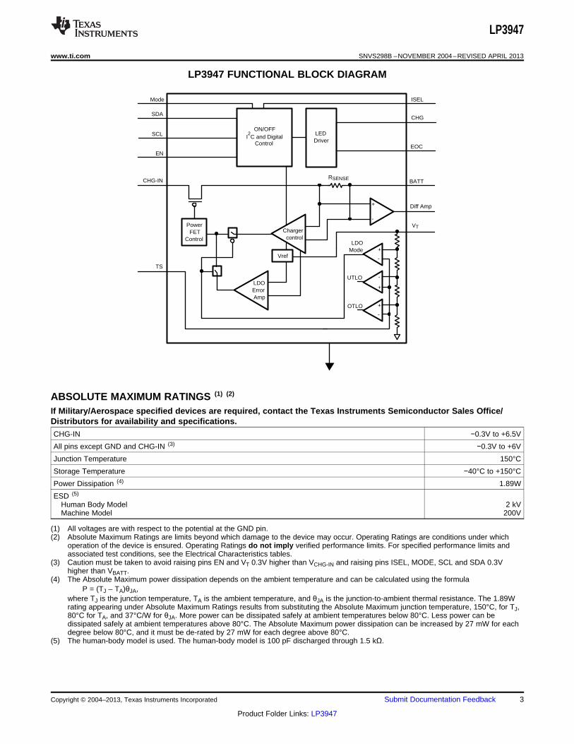
Chargercontrol
TS
CHG-IN
EN
SCL
SDA
Mode
+
-
RSENSE
Vref+
-
-
+
+
-
ISEL
CHG
BATT
Diff Amp
VT
EOC
I2C and Digital
ON/OFF
Control
LEDDriver
PowerFET
ControlLDO
Mode
UTLO
OTLO
LDOErrorAmp
LP3947
www.ti.com SNVS298B –NOVEMBER 2004–REVISED APRIL 2013
LP3947 FUNCTIONAL BLOCK DIAGRAM
ABSOLUTE MAXIMUM RATINGS (1) (2)
If Military/Aerospace specified devices are required, contact the Texas Instruments Semiconductor Sales Office/Distributors for availability and specifications.CHG-IN −0.3V to +6.5V
All pins except GND and CHG-IN (3) −0.3V to +6V
Junction Temperature 150°C
Storage Temperature −40°C to +150°C
Power Dissipation (4) 1.89W
ESD (5)
Human Body Model 2 kVMachine Model 200V
(1) All voltages are with respect to the potential at the GND pin.(2) Absolute Maximum Ratings are limits beyond which damage to the device may occur. Operating Ratings are conditions under which
operation of the device is ensured. Operating Ratings do not imply verified performance limits. For specified performance limits andassociated test conditions, see the Electrical Characteristics tables.
(3) Caution must be taken to avoid raising pins EN and VT 0.3V higher than VCHG-IN and raising pins ISEL, MODE, SCL and SDA 0.3Vhigher than VBATT.
(4) The Absolute Maximum power dissipation depends on the ambient temperature and can be calculated using the formulaMM P = (TJ – TA)θJA,where TJ is the junction temperature, TA is the ambient temperature, and θJA is the junction-to-ambient thermal resistance. The 1.89Wrating appearing under Absolute Maximum Ratings results from substituting the Absolute Maximum junction temperature, 150°C, for TJ,80°C for TA, and 37°C/W for θJA. More power can be dissipated safely at ambient temperatures below 80°C. Less power can bedissipated safely at ambient temperatures above 80°C. The Absolute Maximum power dissipation can be increased by 27 mW for eachdegree below 80°C, and it must be de-rated by 27 mW for each degree above 80°C.
(5) The human-body model is used. The human-body model is 100 pF discharged through 1.5 kΩ.
Copyright © 2004–2013, Texas Instruments Incorporated Submit Documentation Feedback 3
Product Folder Links: LP3947

LP3947
SNVS298B –NOVEMBER 2004–REVISED APRIL 2013 www.ti.com
RECOMMENDED OPERATING CONDITIONS (1) (2)
CHG-IN 0.3V to 6.5V
EN, ISEL, MODE, SCL, SDA, VT(3) 0V to 6V
Junction Temperature −40°C to +125°C
Operating Temperature −40°C to +85°C
Thermal Resistance θJA 37°C/W
Maximum Power Dissipation (4) 1.21W
(1) Absolute Maximum Ratings are limits beyond which damage to the device may occur. Operating Ratings are conditions under whichoperation of the device is ensured. Operating Ratings do not imply verified performance limits. For specified performance limits andassociated test conditions, see the Electrical Characteristics tables.
(2) All voltages are with respect to the potential at the GND pin.(3) Caution must be taken to avoid raising pins EN and VT 0.3V higher than VCHG-IN and raising pins ISEL, MODE, SCL and SDA 0.3V
higher than VBATT.(4) Like the Absolute Maximum power dissipation, the maximum power dissipation for operation depends on the ambient temperature. The
1.21W rating appearing under Operating Ratings results from substituting the maximum junction temperature for operation, 125°C, forTJ, 80°C for TA, and 37°C/W for θJA into (1) above. More power can be dissipated at ambient temperatures below 80°C. Less power canbe dissipated at ambient temperatures above 80°C. The maximum power dissipation for operation can be increased by 27 mW for eachdegree below 80°C, and it must be de-rated by 27 mW for each degree above 80°C.
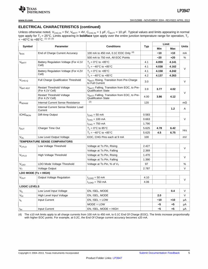
ELECTRICAL CHARACTERISTICSUnless otherwise noted, VCHG-IN = 5V, VBATT = 4V, CCHG-IN = 1 µF, CBATT = 10 µF. Typical values and limits appearing in normaltype apply for TJ = 25°C. Limits appearing in boldface type apply over the entire junction temperature range for operation, TJ
= −40°C to +85°C. (1) (2) (3)
LimitSymbol Parameter Conditions Typ Units
Min Max
VCC SUPPLY
VCHG-IN Input Voltage Range 4.5 6V
VUSB 4.3 6
ICC Quiescent Current VCHG-IN ≤ 4V 2 20µAEOC = Low, adaptor connected, VBATT = 50 1504.1V
VOK-TSHD Adaptor OK Trip Point (CHG-IN) VCHG-IN –VBATT (Rising) 60 mV
VCHG-IN –VBATT (Falling) 50 mV
VUVLO-TSHD Under Voltage Lock-Out Trip Point VCHG-IN (Rising) 3.95 3.6 4.3 V
VCHG-IN (Falling) 3.75 3.4 4.1 V
VOVLO-TSHD Over Voltage Lock-Out Trip Point VCHG-IN (Rising) 5.9V
VCHG-IN (Falling) 5.7
Thermal Shutdown Temperature (2) 160°C
Thermal Shutdown Hysteresis 20
BATTERY CHARGER
ICHG Fast Charge Current Range ISEL = High, In USB Mode 100
ISEL = Low, In USB Mode 500 mA
In AC Adaptor Mode 100 750
Fast Charge Current Accuracy ICHARGE = 100 mA or 150 mA −20 +20 mA
ICHARGE ≥ 200 mA −10 +10 %
IPRE-CHG Pre-Charge Current VBATT = 2V 45 70 mA
(1) All limits are specified. All electrical characteristics having room-temperature limits are tested during production with TJ = 25°C. All hotand cold limits are specified by correlating the electrical characteristics to process and temperature variations and applying statisticalprocess control.
(2) Specified by design.(3) LP3947 is not intended as a Li-Ion battery protection device, any battery used in this application should have an adequate internal
protection.
4 Submit Documentation Feedback Copyright © 2004–2013, Texas Instruments Incorporated
Product Folder Links: LP3947
LP3947
www.ti.com SNVS298B –NOVEMBER 2004–REVISED APRIL 2013
ELECTRICAL CHARACTERISTICS (continued)Unless otherwise noted, VCHG-IN = 5V, VBATT = 4V, CCHG-IN = 1 µF, CBATT = 10 µF. Typical values and limits appearing in normaltype apply for TJ = 25°C. Limits appearing in boldface type apply over the entire junction temperature range for operation, TJ
= −40°C to +85°C. (1) (2) (3)
LimitSymbol Parameter Conditions Typ Units
Min Max
IEOC End of Charge Current Accuracy 100 mA to 450 mA, 0.1C EOC Only (4) −10 +10 mA
500 mA to 750 mA, All EOC Points −20 +20 %
VBATT Battery Regulation Voltage (For 4.1V TJ = 0°C to +85°C 4.1 4.059 4.141Cell) TJ = −40°C to +85°C 4.1 4.038 4.162
VBattery Regulation Voltage (For 4.2V TJ = 0°C to +85°C 4.1 4.158 4.242Cell) TJ = −40°C to +85°C 4.2 4.137 4.263
VCHG-Q Full Charge Qualification Threshold VBATT Rising, Transition from Pre-Charge 3.0 Vto Full Current
VBAT-RST Restart Threshold Voltage VBATT Falling, Transition from EOC, to Pre- 3.9 3.77 4.02(For 4.1V Cell) Qualification StateV
Restart Threshold Voltage VBATT Falling, Transition from EOC, to Pre- 4.00 3.86 4.12(For 4.2V Cell) Qualification State
RSENSE Internal Current Sense Resistance (2) 120 mΩInternal Current Sense Resistor Load 1.2 ACurrent
ICHGMON Diff-Amp Output ICHG = 50 mA 0.583
ICHG = 100 mA 0.663 V
ICHG = 750 mA 1.790
tOUT Charger Time Out TJ = 0°C to 85°C 5.625 4.78 6.42Hrs
TJ = −40°C to +85°C 5.625 4.5 6.75
VOL Low Level Output Voltage EOC, CHG Pins each at 9 mA 100 mV
TEMPERATURE SENSE COMPARATORS
VUTLO Low Voltage Threshold Voltage at Ts Pin, Rising 2.427V
Voltage at Ts Pin, Falling 2.369
VOTLO High Voltage Threshold Voltage at Ts Pin, Rising 1.470V
Voltage at Ts Pin, Falling 1.390
VLDO LDO Mode Voltage Threshold Voltage at Ts Pin, % of VT 97 %
VT Voltage Output 2.787 V
LDO MODE (Ts = HIGH)
VOUT Output Voltage Regulation ILOAD = 50 mA 4.10V
ILOAD = 750 mA 4.06
LOGIC LEVELS
VIL Low Level Input Voltage EN, ISEL, MODE 0.4 V
VIH High Level Input Voltage EN, ISEL, MODE 2.0 V
IIL Input Current EN, ISEL = LOW −10 +10 µA
MODE = LOW −5 +5 µA
IIH Input Current EN, ISEL, MODE = HIGH −5 +5 µA
(4) The ±10 mA limits apply to all charge currents from 100 mA to 450 mA, to 0.1C End Of Charge (EOC). The limits increase proportionallywith higher EOC points. For example, at 0.2C, the End Of Charge current accuracy becomes ±20 mA.
Copyright © 2004–2013, Texas Instruments Incorporated Submit Documentation Feedback 5
Product Folder Links: LP3947

1C4.1V
3.9V
3V
Prequalification to FastCharge transition
BatteryVoltage
BatteryCurrent
CC to CV transition4.1V 0r 4.2V
Time
ONOFF ON
OFF
50 mA
GLEDRLED
End of ChargeCurrent
0.1C (Default)
Bat
tery
Vol
tage
Cha
rge
Cur
rent
LP3947
SNVS298B –NOVEMBER 2004–REVISED APRIL 2013 www.ti.com
ELECTRICAL CHARACTERISTICS, I2C INTERFACEUnless otherwise noted, VCHG-IN = VDD = 5V, VBATT = 4V. Typical values and limits appearing in normal type apply for TJ =25°C. Limits appearing in boldface type apply over the entire junction temperature range for operation, TJ = −40°C to+125°C. (1) (2) (3)
LimitSymbol Parameter Conditions Typ Units
Min Max
VIL Low Level Input Voltage SDA & SCL (2) 0.4 0.3 VDD V
VIH High Level Input Voltage SDA & SCL (2) 0.7 VDD VDD +0.5 V
VOL Low Level Output Voltage SDA & SCL (2) 0 0.2 VDD V
VHYS Schmitt Trigger Input Hysteresis SDA & SCL (2) 0.1 VDD V
FCLK Clock Frequency (2) 400 kHz
tHOLD Hold Time Repeated START Condition (2) 0.6 µs
tCLK-LP CLK Low Period (2) 1.3 µs
tCLK-HP CLK High Period (2) 0.6 µs
tSU Set-Up Time Repeated START (2)0.6 µsCondition
tDATA-HOLD Data Hold Time (2) 300 ns
tDATA-SU Data Set-Up Time (2) 100 ns
tSU Set-Up Time for STOP Condition (2) 0.6 µs
tTRANS Maximum Pulse Width of Spikes that (2)
must be Suppressed by the Input Filter 50 nsof both DATA & CLK Signals.
(1) All limits are specified. All electrical characteristics having room-temperature limits are tested during production with TJ = 25°C. All hotand cold limits are specified by correlating the electrical characteristics to process and temperature variations and applying statisticalprocess control.
(2) Specified by design.(3) LP3947 is not intended as a Li-Ion battery protection device, any battery used in this application should have an adequate internal
protection.
Figure 2. Li-Ion Charging Profile
6 Submit Documentation Feedback Copyright © 2004–2013, Texas Instruments Incorporated
Product Folder Links: LP3947
1 PF
1k
EN
ISEL
Mode
SCL
SDA
TS
VT
RS
RT
VBSense
BATT
10 PFLi-Ion
CHG
EOC
GND
CHG-IN
LP3947Wall
Adaptor
ToSystemSupply
USBPort
P-Ch
MOSFET
Diff-Amp
10k
LP3947
www.ti.com SNVS298B –NOVEMBER 2004–REVISED APRIL 2013
APPLICATION NOTES
LP3947 CHARGER OPERATION
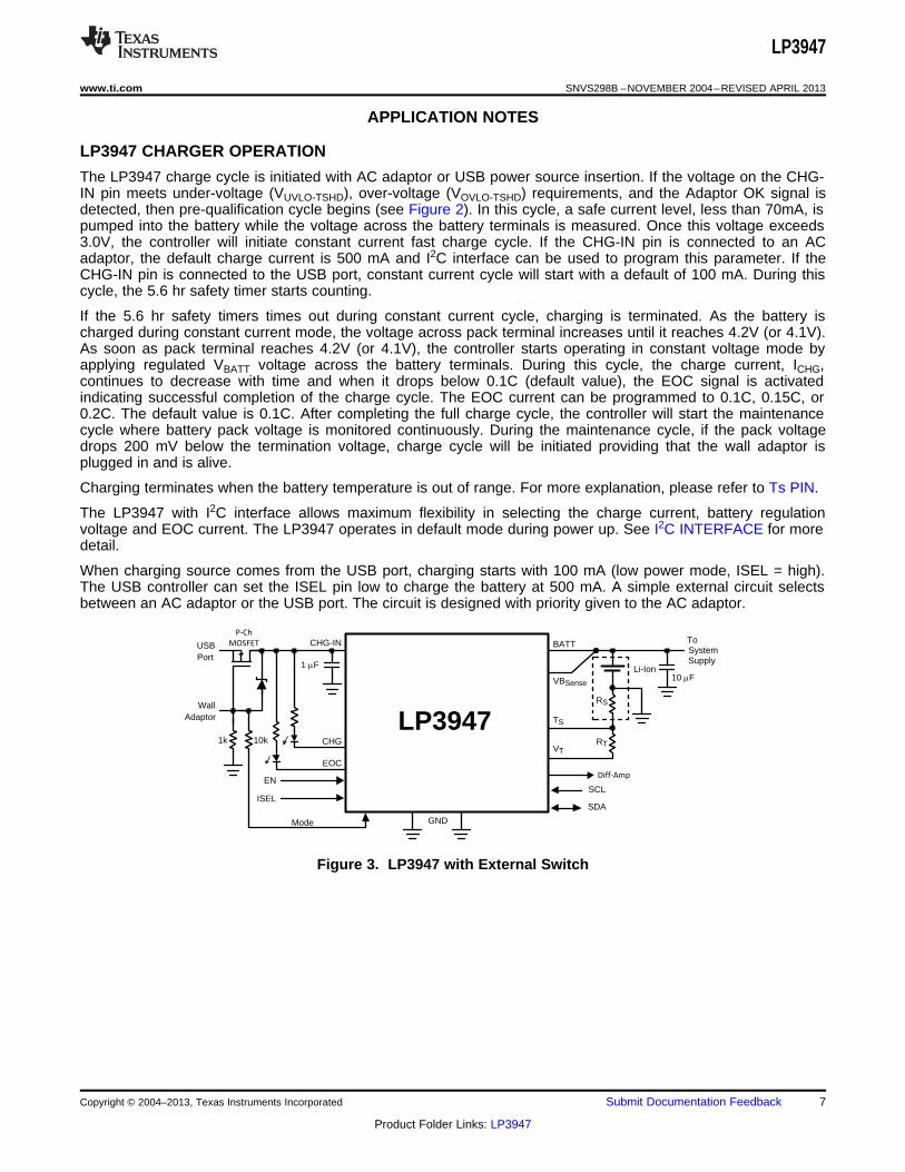
The LP3947 charge cycle is initiated with AC adaptor or USB power source insertion. If the voltage on the CHG-IN pin meets under-voltage (VUVLO-TSHD), over-voltage (VOVLO-TSHD) requirements, and the Adaptor OK signal isdetected, then pre-qualification cycle begins (see Figure 2). In this cycle, a safe current level, less than 70mA, ispumped into the battery while the voltage across the battery terminals is measured. Once this voltage exceeds3.0V, the controller will initiate constant current fast charge cycle. If the CHG-IN pin is connected to an ACadaptor, the default charge current is 500 mA and I2C interface can be used to program this parameter. If theCHG-IN pin is connected to the USB port, constant current cycle will start with a default of 100 mA. During thiscycle, the 5.6 hr safety timer starts counting.
If the 5.6 hr safety timers times out during constant current cycle, charging is terminated. As the battery ischarged during constant current mode, the voltage across pack terminal increases until it reaches 4.2V (or 4.1V).As soon as pack terminal reaches 4.2V (or 4.1V), the controller starts operating in constant voltage mode byapplying regulated VBATT voltage across the battery terminals. During this cycle, the charge current, ICHG,continues to decrease with time and when it drops below 0.1C (default value), the EOC signal is activatedindicating successful completion of the charge cycle. The EOC current can be programmed to 0.1C, 0.15C, or0.2C. The default value is 0.1C. After completing the full charge cycle, the controller will start the maintenancecycle where battery pack voltage is monitored continuously. During the maintenance cycle, if the pack voltagedrops 200 mV below the termination voltage, charge cycle will be initiated providing that the wall adaptor isplugged in and is alive.
Charging terminates when the battery temperature is out of range. For more explanation, please refer to Ts PIN.
The LP3947 with I2C interface allows maximum flexibility in selecting the charge current, battery regulationvoltage and EOC current. The LP3947 operates in default mode during power up. See I2C INTERFACE for moredetail.
When charging source comes from the USB port, charging starts with 100 mA (low power mode, ISEL = high).The USB controller can set the ISEL pin low to charge the battery at 500 mA. A simple external circuit selectsbetween an AC adaptor or the USB port. The circuit is designed with priority given to the AC adaptor.
Figure 3. LP3947 with External Switch
Copyright © 2004–2013, Texas Instruments Incorporated Submit Documentation Feedback 7
Product Folder Links: LP3947

Timer time outCharger = OffTimer resetsRLED = ONGLED = ON
Disconnectpower at
CHG-IN pin torestart charger
Maintenance ModeCharger = OffRLED = OffGLED = On
1.39V<Ts<2.42V?
Battery Tempviolation
Charger = OffTimer resetsRLED = ONGLED = ON
Set Fast Charge Current = IStart 5.6 hr Timer
Timer =5.6 hr?
EN pin =low?
Y
N
1.39V<Ts<2.42V?
N
Y
Y
N
Y
N
N
Y
VBATT > = 4.1V*?
1.39V<Ts<2.42V?
N
Y
1.39V<Ts<2.42V?
N
Y
Constant Voltage ModeVBATT = 4.1V *
Pre-QualificationCharge Current = 50 mA
RLED = OnGLED = Off
1.39V<Ts<2.42V?
N
Y
LDO ModeICHG = 1.2A
VBATT = 4.1V*
LED's Off
4.3V < VCHG-IN < 6.0Vand
VBATT < VCHG-IN
1.39V < Ts < 2.42V
4.3V < VCHG-IN < 6V
Ts t2.7V
VBATT > VCHG-IN
LED's OffCharger Off
1.39V<Ts<2.42V?
N
Y
Timer =5.6 hr?
EN pin =low?
Y
N
or
VBATT > 3.0V?N
IEOC < (0.1 x ICHG)*?N
* Default Value. See "I2C Interface" section.
Y
VBATT > 3.0V?NY
VBATT < 3.9V
EN pin =High?
Yand
N
Y
LP3947
SNVS298B –NOVEMBER 2004–REVISED APRIL 2013 www.ti.com
Figure 4. LP3947 Charger Flow Chart
8 Submit Documentation Feedback Copyright © 2004–2013, Texas Instruments Incorporated
Product Folder Links: LP3947

CHG-IN BattRSense
Diff-Amp
120 m:
0.583V
50 mACharge Current
750 mA
1.74V
Diff
-Am
pO
utpu
t
ICHG = (VDIFF - 0.497)
1.655
LP3947
www.ti.com SNVS298B –NOVEMBER 2004–REVISED APRIL 2013
CHARGE CURRENT SELECTION IN CONSTANT CURRENT MODE
In the AC adaptor mode, the LP3947 is designed to provide a charge current ranging from 100 mA to 750 mA, insteps of 50 mA, to support batteries with different capacity ratings. The default value is 500 mA. No externalresistor is required to set the charge current in the LP3947. In the USB mode, the LP3947 will initially chargewith 100 mA (ISEL = high). By setting the ISEL pin low, charge current can be programmed to 500 mA. Inaddition, with ISEL = low, the charge current can be programmed to different values via the I2C interface.
Table 2. Charge Current Selection in AC Adaptor/USB Mode
MODE Pin ISEL Pin Functions
AC Adaptor Mode HIGH HIGH ISEL polarity is irrelevant. Default 500 mA charge current. Can be reprogrammed viaI2C.HIGH LOW
USB Mode LOW HIGH 100 mA charge current
LOW LOW Default 500 mA charge current. Can be reprogrammed via I2C.
BATTERY VOLTAGE SELECTION
The battery voltage regulation can be set to 4.1V or 4.2V by default. Please refer to Ordering Information formore details.
END OF CHARGE (EOC) CURRENT SELECTION
The EOC thresholds can be programmed to 0.1C, 0.15C or 0.2C in the LP3947. The default value is 0.1C, whichprovides the highest energy storage, but at the expense of longer charging time. On the other hand, 0.2C takesthe least amount of charging time, but yields the least energy storage.
CHARGE CURRENT SENSE DIFFERENTIAL AMPLIFIER
The charge current is monitored across the internal 120 mΩ current sense resistor. The differential amplifierprovides the analog representation of the charge current. Charge current can be calculated using the followingequation:
(1)
Where voltage at Diff Amp output (VDIFF) is in volt, and charge current (ICHG) is in amps.
Figure 5. Charge Current Monitoring Circuit (Diff-Amp)
Monitoring the Diff Amp output during constant voltage cycle can provide an accurate indication of the batterycharge status and time remaining to EOC. This feature is particularly useful during constant voltage mode. Thecurrent sense circuit is operational in the LDO mode as well. It can be used to monitor the system currentconsumption during testing.
LED CHARGE STATUS INDICATORS
The LP3947 is equipped with two open drain outputs to drive a green LED and a red LED. These two LEDs worktogether in combinations to indicate charge status or fault conditions. Table 3 shows all the conditions.
Copyright © 2004–2013, Texas Instruments Incorporated Submit Documentation Feedback 9
Product Folder Links: LP3947

LP3947
SNVS298B –NOVEMBER 2004–REVISED APRIL 2013 www.ti.com
Table 3. LED Indicator Summary
RED LED GREEN LED (EOC)(CHG)
Charger Off OFF OFF
Charging Li Ion Battery (1) ON OFF
Maintenance Mode OFF ON
Charging Li Ion Battery after Passing Maintenance Mode OFF ON
EN Pin = LOW OFF ON
LDO Mode OFF OFF
5.6 Hr Safety Timer Flag/Battery Temperature Violation ON ON
(1) Charging Li Ion battery for the first time after VCHG-IN insertion.
Ts PIN
The LP3947 continuously monitors the battery temperature by measuring the voltage between the Ts pin andground. Charging stops if the battery temperature is outside the permitted temperature range set by the battery’sinternal thermistor RT and the external bias resistor RS. A 1% precision resistor should be used for RS. A curve 2type thermistor is recommended for RT. The voltage across RT is proportional to the battery temperature. If thebattery temperature is outside of the range during the charge cycle, the LP3947 will suspend charging. As anexample, for a temperature range of 0°C to 50°C, a 10kΩ for the thermistor and a 4.1kΩ for Rs should be used.When battery temperature returns to the permitted range, charging resumes from the beginning of the flow chartand the 5.6 hr safety timer is reset. Refer to Figure 4. LP3947 Charger Flow Chart for more information.
In absence of the thermistor, Ts pin will be pulled high to VT and the LP3947 goes into LDO mode. In this mode,the internal power FET provides up to 1.2 amp of current at the BATT pin. The LDO output is set to 4.1V or 4.2V,depending on the programmed battery regulation voltage. When operating at higher output currents, care mustbe taken not to exceed the package power dissipation rating. See “Thermal Performance of WSON Package”section for more detail.
Table 4. Charger Status in Relation to Ts Voltage
Voltage on the Ts Pin Charger Status
Ts ≥ 2.7V LDO Mode
2.427v ≤ Ts < 2.7V Charger Off0V ≤ Ts ≤ 1.39V
1.39V < Ts < 2.427V Charger On
LDO MODE
The charger is in the LDO mode when the Ts pin is left floating. This mode of operation is used primarily duringsystem level testing of the handset to eliminate the need for battery insertion. CAUTION: battery may bedamaged if device is operating in LDO mode with battery connected.
The internal power FET provides up to 1.2 amp of current at BATT pin in this mode. The LDO output is set to4.1V. When operating at higher output currents, care must be taken not to exceed the package power dissipationrating. See “Thermal Performance of WSON Package” section for more detail.
EN PIN
The Enable pin is used to enable/disable the charger, in both the charger mode and the LDO mode, see Figure 6Figure 7. The enable pin is internally pulled HIGH to the CHG-IN pin. When the charger is disabled, it draws lessthan 4 µA of current.
10 Submit Documentation Feedback Copyright © 2004–2013, Texas Instruments Incorporated
Product Folder Links: LP3947

00 TimeTime
0
0
4.1V
0
0
0
4.1V
0
VCHG-IN
VCHG-IN
CH
G-I
NE
NV
BA
TT
VCHG-IN
VCHG-IN
CH
G-I
NE
NV
BA
TT
Load < 50 mA
Load > 50 mA
00 TimeTime
0
0
4.1V
3.0V
0
VCHG-IN
0
VCHG-IN
0
3.0V
0
CH
G-I
NE
NV
BA
TT
VCHG-IN
VCHG-INC
HG
-IN
EN
VB
AT
T
LP3947
www.ti.com SNVS298B –NOVEMBER 2004–REVISED APRIL 2013
Figure 6. Power Up Timing Diagram in Charger Mode (1.39V < Ts < 2.427V)
Figure 7. Power Up Timing Diagram in LDO Mode (Ts ≥ 2.7V)
MODE PIN
The mode pin toggles the LP3947 between the AC adaptor mode and the USB mode. When CHG-IN isconnected to a USB port, this pin must be set low. When CHG-IN is connected to an AC adaptor, this pin mustbe tied high to either the BATT pin or to the wall adaptor input. Caution: MODE pin should never be tied to CHG-IN pin directly, as it will turn on an internal diode.
5.6 HR SAFETY TIMER IN CHARGER MODE
The LP3947 has a built-in 5.6 hr back up safety timer to prevent over-charging a Li Ion battery. The 5.6 hr timerstarts counting when the charger enters the constant current mode. It will turn the charger off when the 5.6 hrtimer is up while the charger is still in constant current mode. In this case, both LEDs will turn on, indicating afault condition.
When the battery temperature is outside the specified temperature range, the 5.6 hr safety timer will reset uponrecovery of the battery temperature.
I2C INTERFACE
I2C interface is used in the LP3947 to program various parameters as shown in Table 5. The LP3947 operateson default settings following power up. Once programmed, the LP3947 retains the register data as long as thebattery voltage is above 2.85V.
Copyright © 2004–2013, Texas Instruments Incorporated Submit Documentation Feedback 11
Product Folder Links: LP3947

ackaddress h´00 dataackaddr = h´00ackwid = h´47start
scl
sda
start msb ID lsb w ack msb ADDRESS lsb ack msb DATA lsb ack
ack from slave ack from slave ack from slave
stop
LP3947
SNVS298B –NOVEMBER 2004–REVISED APRIL 2013 www.ti.com
Table 5. LP3947 Serial Port Communication address code 7h’47
LP3947 Control and Data Codes (1)
Addrs Register 7 6 5 4 3 2 1 0
8′h00 Charger Batt Voltage AC Adaptor AC Adaptor AC Adaptor AC AdaptorRegister -1 (0) = 4.1V Charge Charge Current Charge Current Charge Current
1 = 4.2V Current Code 2 (0) Code 1 (0) Code 0 (0)Code 3 (1)
8′h01 Charger EOC Charging EOC EOCRegister -2 (Green LED) (Red LED) SEL-1 SEL-0
R/O R/O (0) (1)
8′h02 Charger USB USB USB USBRegister -3 Charge Charge Current Charge Current Charge Current
Current Code 2 (0) Code 1 (0) Code 0 (0)Code 3 (1)
(1) Numbers in parentheses indicate default setting. “0” bit is set to low state, and “1” bit is set to high state. R/O –Read Only, All other bitsare Read and Write.
Table 6. Charger Current and EOC Current Programming Code
Charger Current End of Charge CurrentData Code Selection Code ISET (mA) Selection Code
4h′00 100
4h′01 150 0.1C
4h′02 200 0.15C
4h′03 250 0.2C
4h′04 300
4h′05 350
4h′06 400
4h′07 450
4h′08 500
4h′09 550
4h′0A 600
4h′0B 650
4h′0C 700
4h′0D 750
w = write (sda = “0”)r = read (sda = “1”)ack = acknowledge (sda pulled low by either master or slave)Nack = No Acknowledgers = repeated start
Figure 8. LP3947 (Slave) Register Write
12 Submit Documentation Feedback Copyright © 2004–2013, Texas Instruments Incorporated
Product Folder Links: LP3947

TJA = TJ - TA
PD
Nack stopaddress h´00 dataackrid = h´47rsackaddr = h´00ackwid = h´47start
scl
sda
start msb ID lsb w ack msb ADDRESS lsb ack rs msb ID lsb r ack msb lsb NA stopDATA
ack from slave repeated startack from slave ack from slave data from slave Nack from master
LP3947
www.ti.com SNVS298B –NOVEMBER 2004–REVISED APRIL 2013
w = write (sda = “0”)r = read (sda = “1”)ack = acknowledge (sda pulled low by either master or slave)Nack = No Acknowledgers = repeated start
Figure 9. LP3947 (Slave) Register Read
THERMAL PERFORMANCE OF WSON PACKAGE
The LP3947 is a monolithic device with an integrated pass transistor. To enhance the power dissipationperformance, the Leadless Lead frame Package, or WSON, is used. The WSON package is designed forimproved thermal performance because of the exposed die attach pad at the bottom center of the package. Itbrings advantage to thermal performance by creating a very direct path for thermal dissipation. Compared to thetraditional leaded packages where the die attach pad is embedded inside the mold compound, the WSONreduces a layer of thermal path.
The thermal advantage of the WSON package is fully realized only when the exposed die attach pad is soldereddown to a thermal land on the PCB board and thermal vias are planted underneath the thermal land. Based on aWSON thermal measurement, junction to ambient thermal resistance (θJA) can be improved by as much as twotimes if a WSON is soldered on the board with thermal land and thermal vias than if not.
An example of how to calculate for WSON thermal performance is shown below:
(2)
By substituting 37°C/W for θJA, 125°C for TJ and 70°C for TA, the maximum power dissipation allowed from thechip is 1.48W. If VCHG-IN is at 5.0V and a 3.0V battery is being charged, then 740 mA of ICHG can safely chargethe battery. More power can be dissipated at ambient temperatures below 70°C. Less power can be dissipated atambient temperatures above 70°C. The maximum power dissipation for operation can be increased by 27 mWfor each degree below 70°C, and it must be de-rated by 27 mW for each degree above 70°C.
LAYOUT CONSIDERATION
The LP3947 has an exposed die attach pad located at the bottom center of the WSON package. It is imperativeto create a thermal land on the PCB board when designing a PCB layout for the WSON package. The thermalland helps to conduct heat away from the die, and the land should be the same dimension as the exposed padon the bottom of the WSON (1:1 ratio). In addition, thermal vias should be added inside the thermal land toconduct more heat away from the surface of the PCB to the ground plane. Typical pitch and outer diameter forthese thermal vias are 1.27 mm and 0.33 mm respectively. Typical copper via barrel plating is 1oz althoughthicker copper may be used to improve thermal performance. The LP3947 bottom pad is connected to ground.Therefore, the thermal land and vias on the PCB board need to be connected to ground.
For more information on board layout techniques, refer to Application Note 1187 (SNOA401) “LeadlessLeadframe Package (LLP).” The application note also discusses package handling, solder stencil, and assembly.
Copyright © 2004–2013, Texas Instruments Incorporated Submit Documentation Feedback 13
Product Folder Links: LP3947

LP3947
SNVS298B –NOVEMBER 2004–REVISED APRIL 2013 www.ti.com
REVISION HISTORY
Changes from Revision A (April 2013) to Revision B Page
• Changed layout of National Data Sheet to TI format .......................................................................................................... 13
14 Submit Documentation Feedback Copyright © 2004–2013, Texas Instruments Incorporated
Product Folder Links: LP3947

PACKAGE OPTION ADDENDUM
www.ti.com 8-Oct-2015
Addendum-Page 1
PACKAGING INFORMATION
Orderable Device Status(1)
Package Type PackageDrawing
Pins PackageQty
Eco Plan(2)
Lead/Ball Finish(6)
MSL Peak Temp(3)
Op Temp (°C) Device Marking(4/5)
Samples
LP3947ISD-09/NOPB ACTIVE WSON NHL 14 1000 Green (RoHS& no Sb/Br)
CU SN Level-1-260C-UNLIM -40 to 85 L00061B
LP3947ISD-51/NOPB ACTIVE WSON NHL 14 1000 Green (RoHS& no Sb/Br)
CU SN Level-1-260C-UNLIM -40 to 85 L00062B
(1) The marketing status values are defined as follows:ACTIVE: Product device recommended for new designs.LIFEBUY: TI has announced that the device will be discontinued, and a lifetime-buy period is in effect.NRND: Not recommended for new designs. Device is in production to support existing customers, but TI does not recommend using this part in a new design.PREVIEW: Device has been announced but is not in production. Samples may or may not be available.OBSOLETE: TI has discontinued the production of the device.
(2) Eco Plan - The planned eco-friendly classification: Pb-Free (RoHS), Pb-Free (RoHS Exempt), or Green (RoHS & no Sb/Br) - please check http://www.ti.com/productcontent for the latest availabilityinformation and additional product content details.TBD: The Pb-Free/Green conversion plan has not been defined.Pb-Free (RoHS): TI's terms "Lead-Free" or "Pb-Free" mean semiconductor products that are compatible with the current RoHS requirements for all 6 substances, including the requirement thatlead not exceed 0.1% by weight in homogeneous materials. Where designed to be soldered at high temperatures, TI Pb-Free products are suitable for use in specified lead-free processes.Pb-Free (RoHS Exempt): This component has a RoHS exemption for either 1) lead-based flip-chip solder bumps used between the die and package, or 2) lead-based die adhesive used betweenthe die and leadframe. The component is otherwise considered Pb-Free (RoHS compatible) as defined above.Green (RoHS & no Sb/Br): TI defines "Green" to mean Pb-Free (RoHS compatible), and free of Bromine (Br) and Antimony (Sb) based flame retardants (Br or Sb do not exceed 0.1% by weightin homogeneous material)
(3) MSL, Peak Temp. - The Moisture Sensitivity Level rating according to the JEDEC industry standard classifications, and peak solder temperature.
(4) There may be additional marking, which relates to the logo, the lot trace code information, or the environmental category on the device.
(5) Multiple Device Markings will be inside parentheses. Only one Device Marking contained in parentheses and separated by a "~" will appear on a device. If a line is indented then it is a continuationof the previous line and the two combined represent the entire Device Marking for that device.
(6) Lead/Ball Finish - Orderable Devices may have multiple material finish options. Finish options are separated by a vertical ruled line. Lead/Ball Finish values may wrap to two lines if the finishvalue exceeds the maximum column width.
Important Information and Disclaimer:The information provided on this page represents TI's knowledge and belief as of the date that it is provided. TI bases its knowledge and belief on informationprovided by third parties, and makes no representation or warranty as to the accuracy of such information. Efforts are underway to better integrate information from third parties. TI has taken andcontinues to take reasonable steps to provide representative and accurate information but may not have conducted destructive testing or chemical analysis on incoming materials and chemicals.TI and TI suppliers consider certain information to be proprietary, and thus CAS numbers and other limited information may not be available for release.

PACKAGE OPTION ADDENDUM
www.ti.com 8-Oct-2015
Addendum-Page 2
In no event shall TI's liability arising out of such information exceed the total purchase price of the TI part(s) at issue in this document sold by TI to Customer on an annual basis.

TAPE AND REEL INFORMATION
*All dimensions are nominal
Device PackageType
PackageDrawing
Pins SPQ ReelDiameter
(mm)
ReelWidth
W1 (mm)
A0(mm)
B0(mm)
K0(mm)
P1(mm)
W(mm)
Pin1Quadrant
LP3947ISD-09/NOPB WSON NHL 14 1000 178.0 12.4 4.3 4.3 1.3 8.0 12.0 Q1
LP3947ISD-51/NOPB WSON NHL 14 1000 178.0 12.4 4.3 4.3 1.3 8.0 12.0 Q1
PACKAGE MATERIALS INFORMATION
www.ti.com 2-Sep-2015
Pack Materials-Page 1

*All dimensions are nominal
Device Package Type Package Drawing Pins SPQ Length (mm) Width (mm) Height (mm)
LP3947ISD-09/NOPB WSON NHL 14 1000 210.0 185.0 35.0
LP3947ISD-51/NOPB WSON NHL 14 1000 210.0 185.0 35.0
PACKAGE MATERIALS INFORMATION
www.ti.com 2-Sep-2015
Pack Materials-Page 2

MECHANICAL DATA
NHL0014B
www.ti.com
SDA14B (Rev A)
IMPORTANT NOTICE
Texas Instruments Incorporated and its subsidiaries (TI) reserve the right to make corrections, enhancements, improvements and otherchanges to its semiconductor products and services per JESD46, latest issue, and to discontinue any product or service per JESD48, latestissue. Buyers should obtain the latest relevant information before placing orders and should verify that such information is current andcomplete. All semiconductor products (also referred to herein as “components”) are sold subject to TI’s terms and conditions of salesupplied at the time of order acknowledgment.TI warrants performance of its components to the specifications applicable at the time of sale, in accordance with the warranty in TI’s termsand conditions of sale of semiconductor products. Testing and other quality control techniques are used to the extent TI deems necessaryto support this warranty. Except where mandated by applicable law, testing of all parameters of each component is not necessarilyperformed.TI assumes no liability for applications assistance or the design of Buyers’ products. Buyers are responsible for their products andapplications using TI components. To minimize the risks associated with Buyers’ products and applications, Buyers should provideadequate design and operating safeguards.TI does not warrant or represent that any license, either express or implied, is granted under any patent right, copyright, mask work right, orother intellectual property right relating to any combination, machine, or process in which TI components or services are used. Informationpublished by TI regarding third-party products or services does not constitute a license to use such products or services or a warranty orendorsement thereof. Use of such information may require a license from a third party under the patents or other intellectual property of thethird party, or a license from TI under the patents or other intellectual property of TI.Reproduction of significant portions of TI information in TI data books or data sheets is permissible only if reproduction is without alterationand is accompanied by all associated warranties, conditions, limitations, and notices. TI is not responsible or liable for such altereddocumentation. Information of third parties may be subject to additional restrictions.Resale of TI components or services with statements different from or beyond the parameters stated by TI for that component or servicevoids all express and any implied warranties for the associated TI component or service and is an unfair and deceptive business practice.TI is not responsible or liable for any such statements.Buyer acknowledges and agrees that it is solely responsible for compliance with all legal, regulatory and safety-related requirementsconcerning its products, and any use of TI components in its applications, notwithstanding any applications-related information or supportthat may be provided by TI. Buyer represents and agrees that it has all the necessary expertise to create and implement safeguards whichanticipate dangerous consequences of failures, monitor failures and their consequences, lessen the likelihood of failures that might causeharm and take appropriate remedial actions. Buyer will fully indemnify TI and its representatives against any damages arising out of the useof any TI components in safety-critical applications.In some cases, TI components may be promoted specifically to facilitate safety-related applications. With such components, TI’s goal is tohelp enable customers to design and create their own end-product solutions that meet applicable functional safety standards andrequirements. Nonetheless, such components are subject to these terms.No TI components are authorized for use in FDA Class III (or similar life-critical medical equipment) unless authorized officers of the partieshave executed a special agreement specifically governing such use.Only those TI components which TI has specifically designated as military grade or “enhanced plastic” are designed and intended for use inmilitary/aerospace applications or environments. Buyer acknowledges and agrees that any military or aerospace use of TI componentswhich have not been so designated is solely at the Buyer's risk, and that Buyer is solely responsible for compliance with all legal andregulatory requirements in connection with such use.TI has specifically designated certain components as meeting ISO/TS16949 requirements, mainly for automotive use. In any case of use ofnon-designated products, TI will not be responsible for any failure to meet ISO/TS16949.
Products ApplicationsAudio www.ti.com/audio Automotive and Transportation www.ti.com/automotiveAmplifiers amplifier.ti.com Communications and Telecom www.ti.com/communicationsData Converters dataconverter.ti.com Computers and Peripherals www.ti.com/computersDLP® Products www.dlp.com Consumer Electronics www.ti.com/consumer-appsDSP dsp.ti.com Energy and Lighting www.ti.com/energyClocks and Timers www.ti.com/clocks Industrial www.ti.com/industrialInterface interface.ti.com Medical www.ti.com/medicalLogic logic.ti.com Security www.ti.com/securityPower Mgmt power.ti.com Space, Avionics and Defense www.ti.com/space-avionics-defenseMicrocontrollers microcontroller.ti.com Video and Imaging www.ti.com/videoRFID www.ti-rfid.comOMAP Applications Processors www.ti.com/omap TI E2E Community e2e.ti.comWireless Connectivity www.ti.com/wirelessconnectivity
Mailing Address: Texas Instruments, Post Office Box 655303, Dallas, Texas 75265Copyright © 2016, Texas Instruments Incorporated


