Low Power Wideband Fractional 8V97051 RF Synthesizer / PLL ...
56
1 ©2018 Integrated Device Technology, Inc. December 5, 2018 Description The 8V97051 is a high-performance Wideband RF Synthesizer / PLL optimized for use as the local oscillator (LO) in Multi-Carrier, Multi-mode FDD, and TDD Base Station radio card. It is offered in a compact 5 5, 32-VFQFN package. The 8V97051 Wideband RF Synthesizer / PLL offers a default Fractional Mode with the option to use it with an Integer mode. It requires an external loop filter. The 8V97051 has an integrated Voltage Controlled Oscillator (VCO) that supports output frequencies from 34.375MHz to 4400MHz, and maintains superior phase noise and spurious performance. RF_OUT [A:B] output drivers have independently programmable output power ranging from –4dBm to +7dBm. The RF_OUT outputs can be muted. The mute function is accessible via a SPI command or mute pin. The operation of the 8V97051 is controlled by writing to registers through a three-wire SPI interface. The device also has an additional option that allows users to read back values from registers by configuring the MUX_OUT pin as a SDO for the SPI interface. The SPI interface is compatible with 1.8V logic and tolerant to 3.3V. In multi-service base stations, very low noise oscillators are required to generate a large variety of frequencies to the mixers while maintaining excellent phase noise performance and low power. The 8V97051 offers a large tuning range capable of providing multi-band local oscillator (LO) frequency synthesis in multi-mode base stations, thus limiting the use of multiple narrow band RF Synthesizers and reducing the BOM complexity and cost. The device can operate over -40°C to +85°C industrial temperature range. Applications • Wireless Infrastructure • Test Equipment • CATV Equipment • Military and Aerospace • Wireless LAN • Clock Generation Features • Dual Differential Outputs • Output frequency range: 34.375MHz to 4400MHz (continuous range) • RF Output Divide by 1, 2, 4, 8, 16, 32, 64 • Open Drain Outputs (see Output Distribution Section) • Fractional-N synthesizer (also supports Integer-N mode) • 16-bit integer and 12-bit fractional (16-bit fractional when using the extended registers) • 3- or 4-wire SPI interface (compatible with 3.3V and 1.8V) • Single 3.3V supply • Logic compatibility: 1.8V • Programmable output power level: -4dBm to +5dBm (up to +7 when using the extended registers) • Mute Function • Ultra low PN for 1.1GHz LO: -143dBc/Hz at 1MHz Offset, (typical) • Lock Detect Indicators • Input Reference frequency: 5MHz to 310MHz • Power Consumption: 380mW (typical) (RF_OUT B disabled) • 32-Lead, 5 5 VFQFN package • Automatic VCO band selection (Autocal feature) • -40°C to +85°C ambient operating temperature • Supports case temperature 105°C operations • Lead-free (RoHS 6) packaging 8V97051 Datasheet Low Power Wideband Fractional RF Synthesizer / PLL
Transcript of Low Power Wideband Fractional 8V97051 RF Synthesizer / PLL ...
1©2018 Integrated Device Technology, Inc. December 5, 2018
DescriptionThe 8V97051 is a high-performance Wideband RF Synthesizer / PLL optimized for use as the local oscillator (LO) in Multi-Carrier, Multi-mode FDD, and TDD Base Station radio card. It is offered in a compact 5 5, 32-VFQFN package.
The 8V97051 Wideband RF Synthesizer / PLL offers a default Fractional Mode with the option to use it with an Integer mode. It requires an external loop filter.
The 8V97051 has an integrated Voltage Controlled Oscillator (VCO) that supports output frequencies from 34.375MHz to 4400MHz, and maintains superior phase noise and spurious performance.
RF_OUT[A:B] output drivers have independently programmable output power ranging from –4dBm to +7dBm. The RF_OUT outputs can be muted. The mute function is accessible via a SPI command or mute pin.
The operation of the 8V97051 is controlled by writing to registers through a three-wire SPI interface. The device also has an additional option that allows users to read back values from registers by configuring the MUX_OUT pin as a SDO for the SPI interface. The SPI interface is compatible with 1.8V logic and tolerant to 3.3V.
In multi-service base stations, very low noise oscillators are required to generate a large variety of frequencies to the mixers while maintaining excellent phase noise performance and low power. The 8V97051 offers a large tuning range capable of providing multi-band local oscillator (LO) frequency synthesis in multi-mode base stations, thus limiting the use of multiple narrow band RF Synthesizers and reducing the BOM complexity and cost. The device can operate over -40°C to +85°C industrial temperature range.
Applications• Wireless Infrastructure
• Test Equipment
• CATV Equipment
• Military and Aerospace
• Wireless LAN
• Clock Generation
Features• Dual Differential Outputs
• Output frequency range: 34.375MHz to 4400MHz (continuous range)
• RF Output Divide by 1, 2, 4, 8, 16, 32, 64
• Open Drain Outputs (see Output Distribution Section)
• Fractional-N synthesizer (also supports Integer-N mode)
• 16-bit integer and 12-bit fractional (16-bit fractional when using the extended registers)
• 3- or 4-wire SPI interface (compatible with 3.3V and 1.8V)
• Single 3.3V supply
• Logic compatibility: 1.8V
• Programmable output power level: -4dBm to +5dBm(up to +7 when using the extended registers)
• Mute Function
• Ultra low PN for 1.1GHz LO: -143dBc/Hz at 1MHz Offset, (typical)
• Lock Detect Indicators
• Input Reference frequency: 5MHz to 310MHz
• Power Consumption: 380mW (typical) (RF_OUTB disabled)
• 32-Lead, 5 5 VFQFN package
• Automatic VCO band selection (Autocal feature)
• -40°C to +85°C ambient operating temperature
• Supports case temperature 105°C operations
• Lead-free (RoHS 6) packaging
8V97051 Datasheet
Low Power Wideband Fractional RF Synthesizer / PLL

2©2018 Integrated Device Technology, Inc. December 5, 2018
8V97051 Datasheet
Table of ContentsDescription . . . . . . . . . . . . . . . . . . . . . . . . . . . . . . . . . . . . . . . . . . . . . . . . . . . . . . . . . . . . . . . . . . . . . . . . . . . . . . . . . . . . . . . . . . . . . . . . . . . .1
Applications . . . . . . . . . . . . . . . . . . . . . . . . . . . . . . . . . . . . . . . . . . . . . . . . . . . . . . . . . . . . . . . . . . . . . . . . . . . . . . . . . . . . . . . . . . . . . . . . . . . .1
Features . . . . . . . . . . . . . . . . . . . . . . . . . . . . . . . . . . . . . . . . . . . . . . . . . . . . . . . . . . . . . . . . . . . . . . . . . . . . . . . . . . . . . . . . . . . . . . . . . . . . . .1
8V97051 Block Diagram . . . . . . . . . . . . . . . . . . . . . . . . . . . . . . . . . . . . . . . . . . . . . . . . . . . . . . . . . . . . . . . . . . . . . . . . . . . . . . . . . . . . . . . . . .6
Pin Assignment . . . . . . . . . . . . . . . . . . . . . . . . . . . . . . . . . . . . . . . . . . . . . . . . . . . . . . . . . . . . . . . . . . . . . . . . . . . . . . . . . . . . . . . . . . . . . . . . .6
Pin Description and Characteristic Tables . . . . . . . . . . . . . . . . . . . . . . . . . . . . . . . . . . . . . . . . . . . . . . . . . . . . . . . . . . . . . . . . . . . . . . . . . . . .7
Table 1. Pin Description . . . . . . . . . . . . . . . . . . . . . . . . . . . . . . . . . . . . . . . . . . . . . . . . . . . . . . . . . . . . . . . . . . . . . . . . . . . . . . . . . . . . . . . . .7
Table 2. Pin Characteristics . . . . . . . . . . . . . . . . . . . . . . . . . . . . . . . . . . . . . . . . . . . . . . . . . . . . . . . . . . . . . . . . . . . . . . . . . . . . . . . . . . . . . .8
Table 3. Supply Pins and Associated Current Return Paths . . . . . . . . . . . . . . . . . . . . . . . . . . . . . . . . . . . . . . . . . . . . . . . . . . . . . . . . . . . . .8
Principles of Operation . . . . . . . . . . . . . . . . . . . . . . . . . . . . . . . . . . . . . . . . . . . . . . . . . . . . . . . . . . . . . . . . . . . . . . . . . . . . . . . . . . . . . . . . . . .9
Synthesizer Programming . . . . . . . . . . . . . . . . . . . . . . . . . . . . . . . . . . . . . . . . . . . . . . . . . . . . . . . . . . . . . . . . . . . . . . . . . . . . . . . . . . . . . . 9
Reference Input Stage . . . . . . . . . . . . . . . . . . . . . . . . . . . . . . . . . . . . . . . . . . . . . . . . . . . . . . . . . . . . . . . . . . . . . . . . . . . . . . . . . . . . . . . . .9
Reference Doubler . . . . . . . . . . . . . . . . . . . . . . . . . . . . . . . . . . . . . . . . . . . . . . . . . . . . . . . . . . . . . . . . . . . . . . . . . . . . . . . . . . . . . . . . . . . .9
Table 4A. Lock Detect Precision (LDP) . . . . . . . . . . . . . . . . . . . . . . . . . . . . . . . . . . . . . . . . . . . . . . . . . . . . . . . . . . . . . . . . . . . . . . . . . . .9
Feedback Divider . . . . . . . . . . . . . . . . . . . . . . . . . . . . . . . . . . . . . . . . . . . . . . . . . . . . . . . . . . . . . . . . . . . . . . . . . . . . . . . . . . . . . . . . . . . . .9
Figure 1. RF Feedback N Divider . . . . . . . . . . . . . . . . . . . . . . . . . . . . . . . . . . . . . . . . . . . . . . . . . . . . . . . . . . . . . . . . . . . . . . . . . . . . . . .10
Table 4B. Fractional Spurs Due to the Quantization Noise . . . . . . . . . . . . . . . . . . . . . . . . . . . . . . . . . . . . . . . . . . . . . . . . . . . . . . . . . . .10
Phase and Frequency Detector (PFD) and Charge Pump . . . . . . . . . . . . . . . . . . . . . . . . . . . . . . . . . . . . . . . . . . . . . . . . . . . . . . . . . . . .11
Figure 2. Simplified PFD Circuit using D-type Flip-flop . . . . . . . . . . . . . . . . . . . . . . . . . . . . . . . . . . . . . . . . . . . . . . . . . . . . . . . . . . . . . .11
PFD Frequency . . . . . . . . . . . . . . . . . . . . . . . . . . . . . . . . . . . . . . . . . . . . . . . . . . . . . . . . . . . . . . . . . . . . . . . . . . . . . . . . . . . . . . . . . . . . . .11
External Loop Filter . . . . . . . . . . . . . . . . . . . . . . . . . . . . . . . . . . . . . . . . . . . . . . . . . . . . . . . . . . . . . . . . . . . . . . . . . . . . . . . . . . . . . . . . . . .11
Phase Detector Polarity . . . . . . . . . . . . . . . . . . . . . . . . . . . . . . . . . . . . . . . . . . . . . . . . . . . . . . . . . . . . . . . . . . . . . . . . . . . . . . . . . . . . . . .11
Charge Pump High-Impedance . . . . . . . . . . . . . . . . . . . . . . . . . . . . . . . . . . . . . . . . . . . . . . . . . . . . . . . . . . . . . . . . . . . . . . . . . . . . . . . . .11
Integrated Low Noise VCO . . . . . . . . . . . . . . . . . . . . . . . . . . . . . . . . . . . . . . . . . . . . . . . . . . . . . . . . . . . . . . . . . . . . . . . . . . . . . . . . . . . . .11
Output Distribution Section . . . . . . . . . . . . . . . . . . . . . . . . . . . . . . . . . . . . . . . . . . . . . . . . . . . . . . . . . . . . . . . . . . . . . . . . . . . . . . . . . . . . .11
Figure 3. Output Clock Distribution . . . . . . . . . . . . . . . . . . . . . . . . . . . . . . . . . . . . . . . . . . . . . . . . . . . . . . . . . . . . . . . . . . . . . . . . . . . . . .12
Figure 4. Output Stage . . . . . . . . . . . . . . . . . . . . . . . . . . . . . . . . . . . . . . . . . . . . . . . . . . . . . . . . . . . . . . . . . . . . . . . . . . . . . . . . . . . . . . .12
Output Matching . . . . . . . . . . . . . . . . . . . . . . . . . . . . . . . . . . . . . . . . . . . . . . . . . . . . . . . . . . . . . . . . . . . . . . . . . . . . . . . . . . . . . . . . . . . . .12
Figure 5. Broadband Matching Termination . . . . . . . . . . . . . . . . . . . . . . . . . . . . . . . . . . . . . . . . . . . . . . . . . . . . . . . . . . . . . . . . . . . . . . .12
Figure 6. Optimal Matching Termination . . . . . . . . . . . . . . . . . . . . . . . . . . . . . . . . . . . . . . . . . . . . . . . . . . . . . . . . . . . . . . . . . . . . . . . . . .12
Band Selection Disable . . . . . . . . . . . . . . . . . . . . . . . . . . . . . . . . . . . . . . . . . . . . . . . . . . . . . . . . . . . . . . . . . . . . . . . . . . . . . . . . . . . . . . . .12
Phase Adjust . . . . . . . . . . . . . . . . . . . . . . . . . . . . . . . . . . . . . . . . . . . . . . . . . . . . . . . . . . . . . . . . . . . . . . . . . . . . . . . . . . . . . . . . . . . . . . . .13
Phase Resync . . . . . . . . . . . . . . . . . . . . . . . . . . . . . . . . . . . . . . . . . . . . . . . . . . . . . . . . . . . . . . . . . . . . . . . . . . . . . . . . . . . . . . . . . . . . . . .13
Figure 7. 12-bit Counter for Fast Lock and Phase Resync . . . . . . . . . . . . . . . . . . . . . . . . . . . . . . . . . . . . . . . . . . . . . . . . . . . . . . . . . . . .13
Fast Lock Function . . . . . . . . . . . . . . . . . . . . . . . . . . . . . . . . . . . . . . . . . . . . . . . . . . . . . . . . . . . . . . . . . . . . . . . . . . . . . . . . . . . . . . . . . . .13
Figure 8. Example of Fast Lock Mode Loop Filter Topology . . . . . . . . . . . . . . . . . . . . . . . . . . . . . . . . . . . . . . . . . . . . . . . . . . . . . . . . . .14
RF Output Power . . . . . . . . . . . . . . . . . . . . . . . . . . . . . . . . . . . . . . . . . . . . . . . . . . . . . . . . . . . . . . . . . . . . . . . . . . . . . . . . . . . . . . . . . . . .14
MUX_OUT . . . . . . . . . . . . . . . . . . . . . . . . . . . . . . . . . . . . . . . . . . . . . . . . . . . . . . . . . . . . . . . . . . . . . . . . . . . . . . . . . . . . . . . . . . . . . . . . . .14
Table 4C. MUX_OUT Pin Configuration . . . . . . . . . . . . . . . . . . . . . . . . . . . . . . . . . . . . . . . . . . . . . . . . . . . . . . . . . . . . . . . . . . . . . . . . . .14
Power-Down Mode . . . . . . . . . . . . . . . . . . . . . . . . . . . . . . . . . . . . . . . . . . . . . . . . . . . . . . . . . . . . . . . . . . . . . . . . . . . . . . . . . . . . . . . . . . .14
Default Power-Up Conditions . . . . . . . . . . . . . . . . . . . . . . . . . . . . . . . . . . . . . . . . . . . . . . . . . . . . . . . . . . . . . . . . . . . . . . . . . . . . . . . . . . .14
Program Modes . . . . . . . . . . . . . . . . . . . . . . . . . . . . . . . . . . . . . . . . . . . . . . . . . . . . . . . . . . . . . . . . . . . . . . . . . . . . . . . . . . . . . . . . . . . . . .14
Table 4D. Control Bits Configuration . . . . . . . . . . . . . . . . . . . . . . . . . . . . . . . . . . . . . . . . . . . . . . . . . . . . . . . . . . . . . . . . . . . . . . . . . . . .14

3©2018 Integrated Device Technology, Inc. December 5, 2018
8V97051 Datasheet
Double Buffering . . . . . . . . . . . . . . . . . . . . . . . . . . . . . . . . . . . . . . . . . . . . . . . . . . . . . . . . . . . . . . . . . . . . . . . . . . . . . . . . . . . . . . . . . . . . 15
Timing Characteristics . . . . . . . . . . . . . . . . . . . . . . . . . . . . . . . . . . . . . . . . . . . . . . . . . . . . . . . . . . . . . . . . . . . . . . . . . . . . . . . . . . . . . . . 15
Figure 9. SPI Write Cycle Timing Diagram . . . . . . . . . . . . . . . . . . . . . . . . . . . . . . . . . . . . . . . . . . . . . . . . . . . . . . . . . . . . . . . . . . . . . . . 15
Figure 10. SPI Read Cycle Timing Diagram . . . . . . . . . . . . . . . . . . . . . . . . . . . . . . . . . . . . . . . . . . . . . . . . . . . . . . . . . . . . . . . . . . . . . . 15
Table 4E. SPI Read / Write Cycle Timing Parameters . . . . . . . . . . . . . . . . . . . . . . . . . . . . . . . . . . . . . . . . . . . . . . . . . . . . . . . . . . . . . . 15
3- or 4-Wire SPI Interface Description . . . . . . . . . . . . . . . . . . . . . . . . . . . . . . . . . . . . . . . . . . . . . . . . . . . . . . . . . . . . . . . . . . . . . . . . . . . 16
Table 4F. SPI Mode Serial Word Structure . . . . . . . . . . . . . . . . . . . . . . . . . . . . . . . . . . . . . . . . . . . . . . . . . . . . . . . . . . . . . . . . . . . . . . . 16
Register Map . . . . . . . . . . . . . . . . . . . . . . . . . . . . . . . . . . . . . . . . . . . . . . . . . . . . . . . . . . . . . . . . . . . . . . . . . . . . . . . . . . . . . . . . . . . . . . . . . 17
Register 0 . . . . . . . . . . . . . . . . . . . . . . . . . . . . . . . . . . . . . . . . . . . . . . . . . . . . . . . . . . . . . . . . . . . . . . . . . . . . . . . . . . . . . . . . . . . . . . . . . 17
Table 5A. Register 0 Bit Allocation . . . . . . . . . . . . . . . . . . . . . . . . . . . . . . . . . . . . . . . . . . . . . . . . . . . . . . . . . . . . . . . . . . . . . . . . . . . . . 17
Table 5B. Register 0: 16-Bit Feedback Divider Integer Value (INT). Function Description . . . . . . . . . . . . . . . . . . . . . . . . . . . . . . . . . . . 17
Table 5C. Register 0: 12-Bit Feedback Divider Fractional Value (FRAC). Function Description . . . . . . . . . . . . . . . . . . . . . . . . . . . . . . 17
Table 5D. Register 0: 3-Bit Control Bits. Function Description . . . . . . . . . . . . . . . . . . . . . . . . . . . . . . . . . . . . . . . . . . . . . . . . . . . . . . . . 18
Register 1 . . . . . . . . . . . . . . . . . . . . . . . . . . . . . . . . . . . . . . . . . . . . . . . . . . . . . . . . . . . . . . . . . . . . . . . . . . . . . . . . . . . . . . . . . . . . . . . . . 18
Table 6A. Register 1 Bit Allocation . . . . . . . . . . . . . . . . . . . . . . . . . . . . . . . . . . . . . . . . . . . . . . . . . . . . . . . . . . . . . . . . . . . . . . . . . . . . . 18
Table 6B. Register 1: 1-Bit BAND_SEL_DISABLE. Function Description . . . . . . . . . . . . . . . . . . . . . . . . . . . . . . . . . . . . . . . . . . . . . . . 18
Table 6C. Register 1: 12-Bit Phase Value (PHASE). Function Description . . . . . . . . . . . . . . . . . . . . . . . . . . . . . . . . . . . . . . . . . . . . . . 18
Table 6D. Register 1: 12-Bit Modulus Value (MOD). Function Description . . . . . . . . . . . . . . . . . . . . . . . . . . . . . . . . . . . . . . . . . . . . . . 19
Table 6E. Register 1: 3-Bit Control Bits. Function Description . . . . . . . . . . . . . . . . . . . . . . . . . . . . . . . . . . . . . . . . . . . . . . . . . . . . . . . . 19
Register 2 . . . . . . . . . . . . . . . . . . . . . . . . . . . . . . . . . . . . . . . . . . . . . . . . . . . . . . . . . . . . . . . . . . . . . . . . . . . . . . . . . . . . . . . . . . . . . . . . . 19
Table 7A. Register 2 Bit Allocation . . . . . . . . . . . . . . . . . . . . . . . . . . . . . . . . . . . . . . . . . . . . . . . . . . . . . . . . . . . . . . . . . . . . . . . . . . . . . 19
Table 7B. Register 2: 2-Bit NOISE MODE. Function Description . . . . . . . . . . . . . . . . . . . . . . . . . . . . . . . . . . . . . . . . . . . . . . . . . . . . . . 19
Table 7C. Register 2: 3-Bit MUX_OUT. Function Description . . . . . . . . . . . . . . . . . . . . . . . . . . . . . . . . . . . . . . . . . . . . . . . . . . . . . . . . . 20
Table 7D. Register 2: 1-Bit REF DOUBLER. Function Description . . . . . . . . . . . . . . . . . . . . . . . . . . . . . . . . . . . . . . . . . . . . . . . . . . . . 20
Table 7E. Register 2: 1-Bit REF DIV2. Function Description . . . . . . . . . . . . . . . . . . . . . . . . . . . . . . . . . . . . . . . . . . . . . . . . . . . . . . . . . 20
Table 7F. Register 2: 10-Bit R COUNTER (R). Function Description . . . . . . . . . . . . . . . . . . . . . . . . . . . . . . . . . . . . . . . . . . . . . . . . . . . 20
Table 7G. Register 2: 1-Bit DOUBLE BUFFER. Function Description . . . . . . . . . . . . . . . . . . . . . . . . . . . . . . . . . . . . . . . . . . . . . . . . . . 20
Table 7H. Register 2: 4-Bit Charge Pump Setting (ICP SETTING). Function Description . . . . . . . . . . . . . . . . . . . . . . . . . . . . . . . . . . . 21
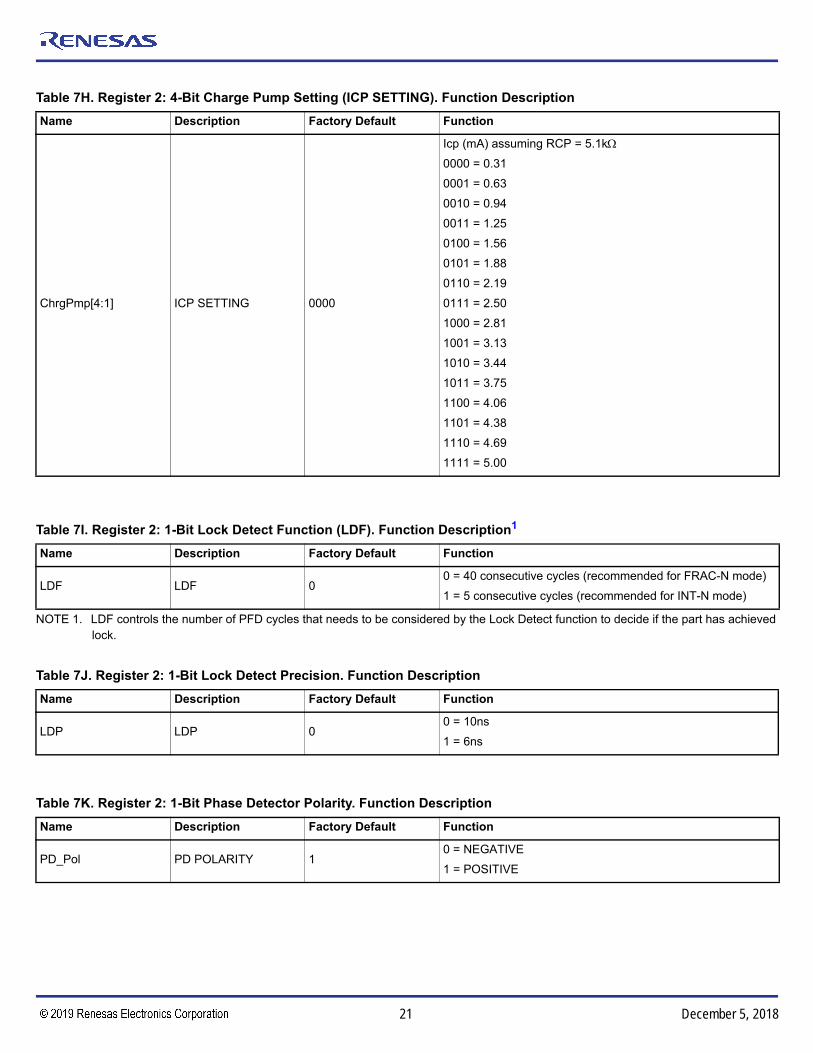
Table 7I. Register 2: 1-Bit Lock Detect Function (LDF). Function Description . . . . . . . . . . . . . . . . . . . . . . . . . . . . . . . . . . . . . . . . . . . . 21
Table 7J. Register 2: 1-Bit Lock Detect Precision. Function Description . . . . . . . . . . . . . . . . . . . . . . . . . . . . . . . . . . . . . . . . . . . . . . . . 21
Table 7K. Register 2: 1-Bit Phase Detector Polarity. Function Description . . . . . . . . . . . . . . . . . . . . . . . . . . . . . . . . . . . . . . . . . . . . . . 21
Table 7L. Register 2: 1-Bit Power Down. Function Description . . . . . . . . . . . . . . . . . . . . . . . . . . . . . . . . . . . . . . . . . . . . . . . . . . . . . . . 22
Table 7M. Register 2: 1-Bit Charge Pump High-Impedance. Function Description . . . . . . . . . . . . . . . . . . . . . . . . . . . . . . . . . . . . . . . . 22
Table 7N. Register 2: 3-Bit Control Bits. Function Description . . . . . . . . . . . . . . . . . . . . . . . . . . . . . . . . . . . . . . . . . . . . . . . . . . . . . . . . 22
Register 3 . . . . . . . . . . . . . . . . . . . . . . . . . . . . . . . . . . . . . . . . . . . . . . . . . . . . . . . . . . . . . . . . . . . . . . . . . . . . . . . . . . . . . . . . . . . . . . . . . 22
Table 8A. Register 3 Bit Allocation . . . . . . . . . . . . . . . . . . . . . . . . . . . . . . . . . . . . . . . . . . . . . . . . . . . . . . . . . . . . . . . . . . . . . . . . . . . . . 22
Table 8B. Register 3: 1-Bit Band Select Clock Mode. Function Description . . . . . . . . . . . . . . . . . . . . . . . . . . . . . . . . . . . . . . . . . . . . . . 23
Table 8C. Register 3: 2-Bit Clock Divider Mode. Function Description . . . . . . . . . . . . . . . . . . . . . . . . . . . . . . . . . . . . . . . . . . . . . . . . . . 23
Table 8D. Register 3: 12-Bit Clock Divider Value (CLKDIV). Function Description . . . . . . . . . . . . . . . . . . . . . . . . . . . . . . . . . . . . . . . . 23
Table 8E. Register 3: 3-Bit Control Bits. Function Description . . . . . . . . . . . . . . . . . . . . . . . . . . . . . . . . . . . . . . . . . . . . . . . . . . . . . . . . 23
Register 4 . . . . . . . . . . . . . . . . . . . . . . . . . . . . . . . . . . . . . . . . . . . . . . . . . . . . . . . . . . . . . . . . . . . . . . . . . . . . . . . . . . . . . . . . . . . . . . . . . 24
Table 9A. Register 4 Bit Allocation . . . . . . . . . . . . . . . . . . . . . . . . . . . . . . . . . . . . . . . . . . . . . . . . . . . . . . . . . . . . . . . . . . . . . . . . . . . . . 24
Table 9B. Register 4: 1-Bit Feedback Select. Function Description . . . . . . . . . . . . . . . . . . . . . . . . . . . . . . . . . . . . . . . . . . . . . . . . . . . . 24
Table 9C. Register 4: 3-Bit RF Output Divider (÷ MO) Select. Function Description . . . . . . . . . . . . . . . . . . . . . . . . . . . . . . . . . . . . . . . 24
Table 9D. Register 4: 8-Bit Band Select Clock Counter. Function Description . . . . . . . . . . . . . . . . . . . . . . . . . . . . . . . . . . . . . . . . . . . . 25
Table 9E. Register 4: 1-Bit VCO Power Down. Function Description . . . . . . . . . . . . . . . . . . . . . . . . . . . . . . . . . . . . . . . . . . . . . . . . . . . 25
Table 9F. Register 4: 1-Bit Mute Till Lock Detect. Function Description . . . . . . . . . . . . . . . . . . . . . . . . . . . . . . . . . . . . . . . . . . . . . . . . . 25

4©2018 Integrated Device Technology, Inc. December 5, 2018
8V97051 Datasheet
Table 9G. Register 4: 1-Bit RF_OUTB Select. Function Description . . . . . . . . . . . . . . . . . . . . . . . . . . . . . . . . . . . . . . . . . . . . . . . . . . . .25
Table 9H. Register 4: 1-Bit RF_OUTB Enable. Function Description . . . . . . . . . . . . . . . . . . . . . . . . . . . . . . . . . . . . . . . . . . . . . . . . . . . .25
Table 9I. Register 4: 2-Bit RF_OUTB Output Power. Function Description . . . . . . . . . . . . . . . . . . . . . . . . . . . . . . . . . . . . . . . . . . . . . . .25
Table 9J. Register 4: 1-Bit RF_OUTA Enable. Function Description . . . . . . . . . . . . . . . . . . . . . . . . . . . . . . . . . . . . . . . . . . . . . . . . . . . .26
Table 9K. Register 4: 2-Bit RF_OUTA Output Power. Function Description . . . . . . . . . . . . . . . . . . . . . . . . . . . . . . . . . . . . . . . . . . . . . . .26
Table 9L. Register 4: 3-Bit Control Bits. Function Description . . . . . . . . . . . . . . . . . . . . . . . . . . . . . . . . . . . . . . . . . . . . . . . . . . . . . . . . .26
Register 5 . . . . . . . . . . . . . . . . . . . . . . . . . . . . . . . . . . . . . . . . . . . . . . . . . . . . . . . . . . . . . . . . . . . . . . . . . . . . . . . . . . . . . . . . . . . . . . . . . .26
Table 10A. Register 5 Bit Allocation . . . . . . . . . . . . . . . . . . . . . . . . . . . . . . . . . . . . . . . . . . . . . . . . . . . . . . . . . . . . . . . . . . . . . . . . . . . . .26
Table 10B. Register 5: 2-Bit LD (Lock Detect) Pin Mode. Function Description . . . . . . . . . . . . . . . . . . . . . . . . . . . . . . . . . . . . . . . . . . . .27
Table 10C. Register 5: 3-Bit Control Bits. Function Description . . . . . . . . . . . . . . . . . . . . . . . . . . . . . . . . . . . . . . . . . . . . . . . . . . . . . . . .27
Extended Registers, (Registers 6 and 7) . . . . . . . . . . . . . . . . . . . . . . . . . . . . . . . . . . . . . . . . . . . . . . . . . . . . . . . . . . . . . . . . . . . . . . . . . .27
Register 6 . . . . . . . . . . . . . . . . . . . . . . . . . . . . . . . . . . . . . . . . . . . . . . . . . . . . . . . . . . . . . . . . . . . . . . . . . . . . . . . . . . . . . . . . . . . . . . . . . .27
Table 11A. Register 6 Bit Allocation . . . . . . . . . . . . . . . . . . . . . . . . . . . . . . . . . . . . . . . . . . . . . . . . . . . . . . . . . . . . . . . . . . . . . . . . . . . .27
Table 11B. Register 6: 1-Bit Digital Lock Detect. Function Description . . . . . . . . . . . . . . . . . . . . . . . . . . . . . . . . . . . . . . . . . . . . . . . . . .28
Table 11C. Register 6: 1-Bit Band Select Status (Read Only). Function Description . . . . . . . . . . . . . . . . . . . . . . . . . . . . . . . . . . . . . . . .28
Table 11D. Register 6: 2-Bit Extra Lock Detect Precision. Function Description . . . . . . . . . . . . . . . . . . . . . . . . . . . . . . . . . . . . . . . . . . .28
Table 11E. Register 6: 1-Bit Extra Bit of RF_OUTB Power. Function Description . . . . . . . . . . . . . . . . . . . . . . . . . . . . . . . . . . . . . . . . . .29
Table 11F. Register 6: 1-Bit Extra Bit of RF_OUTA Power. Function Description . . . . . . . . . . . . . . . . . . . . . . . . . . . . . . . . . . . . . . . . . . .29
Table 11G. Register 6: 2-Bit Sigma Delta Modulator Order Configuration. Function Description . . . . . . . . . . . . . . . . . . . . . . . . . . . . . . .29
Table 11H. Register 6: 2-Bit Dither Gain Configuration. Function Description . . . . . . . . . . . . . . . . . . . . . . . . . . . . . . . . . . . . . . . . . . . . .30
Table 11I. Register 6: 1-Bit Dither Noise Shaping Configuration. Function Description . . . . . . . . . . . . . . . . . . . . . . . . . . . . . . . . . . . . . .30
Table 11J. Register 6: 1-Bit Sigma Delta Modulator Type Configuration. Function Description . . . . . . . . . . . . . . . . . . . . . . . . . . . . . . . .30
Table 11K. Register 6: 2-Bit VCO Band Selection Accuracy Configuration. Function Description . . . . . . . . . . . . . . . . . . . . . . . . . . . . . .30
Table 11L. Register 6: 4-Bit Extra Most Significant Bits of Band Select Divider. Function Description . . . . . . . . . . . . . . . . . . . . . . . . .30
Table 11M. Register 6: 3-Bit Control Bits. Function Description . . . . . . . . . . . . . . . . . . . . . . . . . . . . . . . . . . . . . . . . . . . . . . . . . . . . . . . .30
Register 7 . . . . . . . . . . . . . . . . . . . . . . . . . . . . . . . . . . . . . . . . . . . . . . . . . . . . . . . . . . . . . . . . . . . . . . . . . . . . . . . . . . . . . . . . . . . . . . . . . .31
Table 12A. Register 7 Bit Allocation. . . . . . . . . . . . . . . . . . . . . . . . . . . . . . . . . . . . . . . . . . . . . . . . . . . . . . . . . . . . . . . . . . . . . . . . . . . . . .31
Table 12B. Register 7: 1-Bit Loss of Digital Lock. Function Description . . . . . . . . . . . . . . . . . . . . . . . . . . . . . . . . . . . . . . . . . . . . . . . . . .31
Table 12C. Register 7: 1-Bit Loss of Analog Lock. Function Description . . . . . . . . . . . . . . . . . . . . . . . . . . . . . . . . . . . . . . . . . . . . . . . . .31
Table 12D. Register 7: 1-Bit SPI Error. Function Description . . . . . . . . . . . . . . . . . . . . . . . . . . . . . . . . . . . . . . . . . . . . . . . . . . . . . . . . . .31
Table 12E. Register 7: 3-Bit Revision ID. Function Description . . . . . . . . . . . . . . . . . . . . . . . . . . . . . . . . . . . . . . . . . . . . . . . . . . . . . . . .32
Table 12F. Register 7: 4-Bit Device ID. Function Description . . . . . . . . . . . . . . . . . . . . . . . . . . . . . . . . . . . . . . . . . . . . . . . . . . . . . . . . . .32
Table 12G. Register 7: 1-Bit Resolution Select. Function Description. . . . . . . . . . . . . . . . . . . . . . . . . . . . . . . . . . . . . . . . . . . . . . . . . . . .32
Table 12H. Register 7: 4-Bit Extra Bits of PHASE Value. Function Description . . . . . . . . . . . . . . . . . . . . . . . . . . . . . . . . . . . . . . . . . . . .32
Table 12I. Register 7: 4-Bit Extra Bits of MOD Value. Function Description . . . . . . . . . . . . . . . . . . . . . . . . . . . . . . . . . . . . . . . . . . . . . . .33
Table 12J. Register 7: 4-Bit Extra Bits of FRAC Value. Function Description . . . . . . . . . . . . . . . . . . . . . . . . . . . . . . . . . . . . . . . . . . . . . .33
Table 12K. Register 7: 1-Bit SCLKE. Function Description . . . . . . . . . . . . . . . . . . . . . . . . . . . . . . . . . . . . . . . . . . . . . . . . . . . . . . . . . . .34
Table 12L. Register 7: 1-Bit READBACK_ADDR. Function Description . . . . . . . . . . . . . . . . . . . . . . . . . . . . . . . . . . . . . . . . . . . . . . . . .34
Table 12M. Register 7: 1-Bit SPI_R_WN. Function Description . . . . . . . . . . . . . . . . . . . . . . . . . . . . . . . . . . . . . . . . . . . . . . . . . . . . . . . .34
Table 12N. Register 7: 3-Bit Control Bits. Function Description . . . . . . . . . . . . . . . . . . . . . . . . . . . . . . . . . . . . . . . . . . . . . . . . . . . . . . . .34
Absolute Maximum Ratings . . . . . . . . . . . . . . . . . . . . . . . . . . . . . . . . . . . . . . . . . . . . . . . . . . . . . . . . . . . . . . . . . . . . . . . . . . . . . . . . . . . . . .35
Table 13. Absolute Maximum Ratings . . . . . . . . . . . . . . . . . . . . . . . . . . . . . . . . . . . . . . . . . . . . . . . . . . . . . . . . . . . . . . . . . . . . . . . . . . . . .35
DC Electrical Characteristics . . . . . . . . . . . . . . . . . . . . . . . . . . . . . . . . . . . . . . . . . . . . . . . . . . . . . . . . . . . . . . . . . . . . . . . . . . . . . . . . . . . . .36
Table 14A. Power Supply DC Characteristics, VDDX = VDDA = 3.3V ± 5%, TA = -40°C to +85°C . . . . . . . . . . . . . . . . . . . . . . . . . . . . . . . .36
Table 14B. Output Divider Incremental Current . . . . . . . . . . . . . . . . . . . . . . . . . . . . . . . . . . . . . . . . . . . . . . . . . . . . . . . . . . . . . . . . . . . . . .36
Table 14C. Typical Current by Power Domain . . . . . . . . . . . . . . . . . . . . . . . . . . . . . . . . . . . . . . . . . . . . . . . . . . . . . . . . . . . . . . . . . . . . . . .37
Table 14D. LVCMOS DC Characteristics, VDDX = VDDA = 3.3V ± 5%, TA = -40°C to 85°C . . . . . . . . . . . . . . . . . . . . . . . . . . . . . . . . . . . . .37

5©2018 Integrated Device Technology, Inc. December 5, 2018
8V97051 Datasheet
AC Electrical Characteristics . . . . . . . . . . . . . . . . . . . . . . . . . . . . . . . . . . . . . . . . . . . . . . . . . . . . . . . . . . . . . . . . . . . . . . . . . . . . . . . . . . . . .38
Table 15A. AC Characteristics, VDDX = VDDA = 3.3V ± 5%, TA = -40°C to 85°C. . . . . . . . . . . . . . . . . . . . . . . . . . . . . . . . . . . . . . . . . . . . . .38
Table 15B. RF_OUT[A:B] Phase Noise and Jitter Characteristics, VDDX = VDDA = 3.3V ± 5%, TA = -40°C to 85°C . . . . . . . . . . . . . . . . .39
Phase Noise at 156.25MHz (3.3V) . . . . . . . . . . . . . . . . . . . . . . . . . . . . . . . . . . . . . . . . . . . . . . . . . . . . . . . . . . . . . . . . . . . . . . . . . . . . . . . . .41
Phase Noise at 1.76GHz (3.3V) . . . . . . . . . . . . . . . . . . . . . . . . . . . . . . . . . . . . . . . . . . . . . . . . . . . . . . . . . . . . . . . . . . . . . . . . . . . . . . . . . . .41
Phase Noise Performance (Open Loop) at 1.1GHz (3.3V) . . . . . . . . . . . . . . . . . . . . . . . . . . . . . . . . . . . . . . . . . . . . . . . . . . . . . . . . . . . . . .42
Phase Noise Performance (Open Loop) at 1.65GHz (3.3V) . . . . . . . . . . . . . . . . . . . . . . . . . . . . . . . . . . . . . . . . . . . . . . . . . . . . . . . . . . . . .42
Phase Noise Performance (Open Loop) at 2.3GHz (3.3V) . . . . . . . . . . . . . . . . . . . . . . . . . . . . . . . . . . . . . . . . . . . . . . . . . . . . . . . . . . . . . .43
Phase Noise Performance (Open Loop) at 3.8GHz (3.3V) . . . . . . . . . . . . . . . . . . . . . . . . . . . . . . . . . . . . . . . . . . . . . . . . . . . . . . . . . . . . . .43
Applications Information . . . . . . . . . . . . . . . . . . . . . . . . . . . . . . . . . . . . . . . . . . . . . . . . . . . . . . . . . . . . . . . . . . . . . . . . . . . . . . . . . . . . . . . . .44
Loop Filter Calculations . . . . . . . . . . . . . . . . . . . . . . . . . . . . . . . . . . . . . . . . . . . . . . . . . . . . . . . . . . . . . . . . . . . . . . . . . . . . . . . . . . . . . . .44
2nd Order Loop Filter . . . . . . . . . . . . . . . . . . . . . . . . . . . . . . . . . . . . . . . . . . . . . . . . . . . . . . . . . . . . . . . . . . . . . . . . . . . . . . . . . . . . . . .44
Figure 11. Typical 2nd Order Loop Filter . . . . . . . . . . . . . . . . . . . . . . . . . . . . . . . . . . . . . . . . . . . . . . . . . . . . . . . . . . . . . . . . . . . . . . . .44
3rd Order Loop Filter . . . . . . . . . . . . . . . . . . . . . . . . . . . . . . . . . . . . . . . . . . . . . . . . . . . . . . . . . . . . . . . . . . . . . . . . . . . . . . . . . . . . . . . 45
Figure 12. Typical 3rd Order Loop Filter . . . . . . . . . . . . . . . . . . . . . . . . . . . . . . . . . . . . . . . . . . . . . . . . . . . . . . . . . . . . . . . . . . . . . . . .45
Recommendations for Unused Input and Output Pins . . . . . . . . . . . . . . . . . . . . . . . . . . . . . . . . . . . . . . . . . . . . . . . . . . . . . . . . . . . . . . . .45
Schematic Example . . . . . . . . . . . . . . . . . . . . . . . . . . . . . . . . . . . . . . . . . . . . . . . . . . . . . . . . . . . . . . . . . . . . . . . . . . . . . . . . . . . . . . . . . .46
Figure 13A. An 8V97051 General Application Schematic Example . . . . . . . . . . . . . . . . . . . . . . . . . . . . . . . . . . . . . . . . . . . . . . . . . . . . .47
Figure 13B. Schematic Example for Driving Single Ended Mixer . . . . . . . . . . . . . . . . . . . . . . . . . . . . . . . . . . . . . . . . . . . . . . . . . . . . . . .48
Power Considerations . . . . . . . . . . . . . . . . . . . . . . . . . . . . . . . . . . . . . . . . . . . . . . . . . . . . . . . . . . . . . . . . . . . . . . . . . . . . . . . . . . . . . . . . . . .49
Table 16. Thermal Resistance JA for 32 Lead VFQFN, Forced Convection . . . . . . . . . . . . . . . . . . . . . . . . . . . . . . . . . . . . . . . . . . . . . .49
Case Temperature Considerations . . . . . . . . . . . . . . . . . . . . . . . . . . . . . . . . . . . . . . . . . . . . . . . . . . . . . . . . . . . . . . . . . . . . . . . . . . . . .50
Reliability Information . . . . . . . . . . . . . . . . . . . . . . . . . . . . . . . . . . . . . . . . . . . . . . . . . . . . . . . . . . . . . . . . . . . . . . . . . . . . . . . . . . . . . . . . . . .51
Table 17A. JA vs. Air Flow Table for a 32 lead VFQFN . . . . . . . . . . . . . . . . . . . . . . . . . . . . . . . . . . . . . . . . . . . . . . . . . . . . . . . . . . . . . . . .51
Table 17B. JB vs. Air Flow Table for a 32 lead VFQFN . . . . . . . . . . . . . . . . . . . . . . . . . . . . . . . . . . . . . . . . . . . . . . . . . . . . . . . . . . . . . . . .51
Transistor Count . . . . . . . . . . . . . . . . . . . . . . . . . . . . . . . . . . . . . . . . . . . . . . . . . . . . . . . . . . . . . . . . . . . . . . . . . . . . . . . . . . . . . . . . . . . . . . .51
Package Outline Drawings . . . . . . . . . . . . . . . . . . . . . . . . . . . . . . . . . . . . . . . . . . . . . . . . . . . . . . . . . . . . . . . . . . . . . . . . . . . . . . . . . . . . . . .51
Ordering Information . . . . . . . . . . . . . . . . . . . . . . . . . . . . . . . . . . . . . . . . . . . . . . . . . . . . . . . . . . . . . . . . . . . . . . . . . . . . . . . . . . . . . . . . . . . .52
Table 18. Ordering Information . . . . . . . . . . . . . . . . . . . . . . . . . . . . . . . . . . . . . . . . . . . . . . . . . . . . . . . . . . . . . . . . . . . . . . . . . . . . . . . . . .52
Table 19. Pin 1 Orientation in Tape and Reel Packaging . . . . . . . . . . . . . . . . . . . . . . . . . . . . . . . . . . . . . . . . . . . . . . . . . . . . . . . . . . . . . . .52
Revision History. . . . . . . . . . . . . . . . . . . . . . . . . . . . . . . . . . . . . . . . . . . . . . . . . . . . . . . . . . . . . . . . . . . . . . . . . . . . . . . . . . . . . . . . . . . . . . . .53

6©2018 Integrated Device Technology, Inc. December 5, 2018
8V97051 Datasheet
8V97051 Block Diagram
`
x2÷R
16/12 or 16/16 bit Frac-NDivider
SCLKSDICSB
MUTE
LD
Logic & Registers
RF_OUTA
RF_OUTB
÷M0nRF_OUTA
nRF_OUTB
REF_IN÷2
LockDetect
MUX_OUT
SDO
CE
CP_OUT
VTUNE
ExternalLoopFilter
SPI
PFD ChargePump
FLSW
NOTE: 16-Bit Integer / 16-Bit Fractional feedback divider is available when using extended register.
Pin Assignment
32
VVCOGND_CP
GN
DA
V DD
_SD
V DD
A
GN
DA_
VCO
RF_
OU
T A
nRF_
OU
T A
RF_
OU
T B
nRF_
OU
T B
V VC
O
GNDA_VCO
VBIAS
VTUNE
GNDA_VCO
RCP
VCOM
VREF
GN
D_S
D
MU
TE
LDV DD
D
GN
DD
MU
X_O
UT
REF
_IN
CP_OUT
V_CP
FLSW
CE
nCS
SDI
SCLK
8V97051
8
7
6
5
4
3
2
1
17
18
19
20
21
22
23
24
9 10 11 12 13 14 15 16
31 30 29 28 27 26 25
32-Lead 5mm x 5mm VFQFN

7©2018 Integrated Device Technology, Inc. December 5, 2018
8V97051 Datasheet
Pin Description and Characteristic Tables
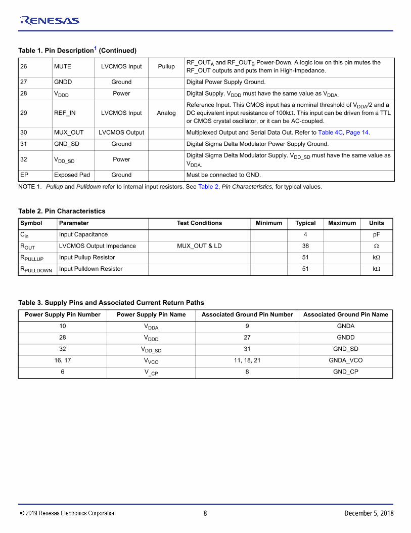
Table 1. Pin Description1
Pin Name Type Description
1 SCLK LVCMOS Input Pulldown Serial Clock Input. High-Impedance CMOS input. 1.8V logic. 3.3V tolerant.
2 SDI LVCMOS Input Pullup Serial Data Input. High-Impedance CMOS input. 1.8V logic. 3.3V tolerant.
3 nCS LVCMOS Input PulldownLoad Enable. High-Impedance CMOS input. 1.8V logic. 3.3V tolerant. Active Low.
4 CE LVCMOS Input PullupChip Enable. On logic Low, powers down the device and puts the charge pump into High-Impedance mode. Powers up the device on logic High.
5 FLSW AnalogFast Lock Switch. A connection should be made from the loop filter to this pin when using the fast lock mode.
6 V_CP PowerCharge Pump Power Supply. V_CP must have the same value as VDDA. Place decoupling capacitors to the ground plane as close to this pin as possible.
7 CP_OUT AnalogCharge Pump Output. When enabled, this output provides ±ICP to the external loop filter. The output of the loop filter is connected to VTUNE to drive the internal VCO.
8 GND_CP Ground Charge Pump Power Supply Ground.
9 GNDA Ground Analog Power Supply Ground.
10 VDDA PowerAnalog Supply. This pin ranges from 3.3V ± 5%. VDDA must have the same value as VDDD.
11 GNDA_VCO Ground VCO Analog Power Supply Ground.
12 RF_OUTA Output Clock Output pair A. The output level is programmable.
13 nRF_OUTA Output Clock Output pair A. The output level is programmable.
14 RF_OUTB Output Clock Output pair B. The output level is programmable.
15 nRF_OUTB Output Clock Output pair B. The output level is programmable.
16 VVCO PowerVCO Supply. This pin ranges from 3.3V ± 5%. VVCO must have the same value as VDDA.
17 VVCO PowerVCO Supply. This pin ranges from 3.3V ± 5%. VVCO must have the same value as VDDA.
18 GNDA_VCO Ground VCO Analog Power Supply Ground.
19 VBIAS AnalogPlace decoupling capacitors (0.1µF) to ground, as close to this pin as possible.
20 VTUNE Control Input to tune the VCO.
21 GNDA_VCO Ground VCO Analog Power Supply Ground.
22 RCP Analog Sets the charge pump current. Requires external resistor.
23 VCOM AnalogPlace decoupling capacitors (0.1µF) to ground, as close to this pin as possible.
24 VREF AnalogPlace decoupling capacitors (0.1µF) to ground, as close to this pin as possible.
25 LD LVCMOS OutputLock Detect. Logic High indicates PLL lock. Logic Low indicates loss of PLL lock.
8©2018 Integrated Device Technology, Inc. December 5, 2018
8V97051 Datasheet
26 MUTE LVCMOS Input PullupRF_OUTA and RF_OUTB Power-Down. A logic low on this pin mutes the RF_OUT outputs and puts them in High-Impedance.
27 GNDD Ground Digital Power Supply Ground.
28 VDDD Power Digital Supply. VDDD must have the same value as VDDA.
29 REF_IN LVCMOS Input AnalogReference Input. This CMOS input has a nominal threshold of VDDA/2 and a DC equivalent input resistance of 100k. This input can be driven from a TTL or CMOS crystal oscillator, or it can be AC-coupled.
30 MUX_OUT LVCMOS Output Multiplexed Output and Serial Data Out. Refer to Table 4C, Page 14.
31 GND_SD Ground Digital Sigma Delta Modulator Power Supply Ground.
32 VDD_SD PowerDigital Sigma Delta Modulator Supply. VDD_SD must have the same value as VDDA.
EP Exposed Pad Ground Must be connected to GND.
NOTE 1. Pullup and Pulldown refer to internal input resistors. See Table 2, Pin Characteristics, for typical values.
Table 1. Pin Description1 (Continued)
Table 2. Pin Characteristics
Symbol Parameter Test Conditions Minimum Typical Maximum Units
Cin Input Capacitance 4 pF
ROUT LVCMOS Output Impedance MUX_OUT & LD 38
RPULLUP Input Pullup Resistor 51 k
RPULLDOWN Input Pulldown Resistor 51 k
Table 3. Supply Pins and Associated Current Return Paths
Power Supply Pin Number Power Supply Pin Name Associated Ground Pin Number Associated Ground Pin Name
10 VDDA 9 GNDA
28 VDDD 27 GNDD
32 VDD_SD 31 GND_SD
16, 17 VVCO 11, 18, 21 GNDA_VCO
6 V_CP 8 GND_CP
9©2018 Integrated Device Technology, Inc. December 5, 2018
8V97051 Datasheet
Principles of Operation
Synthesizer Programming
The Fractional-N architecture is implemented via a cascaded programmable dual modulus prescaler. The N divider offers a division ratio in the feedback path of the PLL, and is given by programming the value of INT, FRAC and MOD in the following equation:
N = INT + FRAC/MOD (1)
INT is the divide ratio of the binary 16-bits counter (refer to Table 5B, Page 17).
FRAC is the numerator value of the fractional divide ratio. It is programmable from 0 to (MOD – 1). Refer to Table 5C when in 12-bit mode, or Table 12J when in 16-bit mode.
MOD is the 12-bit or 16-bit modulus. It is programmable from 2 to 4095 in 12-bit mode, and 2 to 65535 in 16-bit mode. Refer to Table 6D when in 12-bit mode, or Table 12I when in 16-bit mode.
The VCO frequency (fVCO) at RF_OUTA or RF_OUTB is given by the following equation:
fVCO = fPFD x (INT + FRAC/MOD) (2)
fPFD is the frequency at the input of the Phase and Frequency Detector (PFD).
The 8V97051 offers an Integer mode. To enable that mode, the user has to program the FRAC value to 0.
The device’s VCO features three VCO band-splits to cover the entire range with sufficient margin for process, voltage, and temperature variations. These are automatically selected by invoking the Autocal feature. The charge pump current is also programmable via the ICP SETTING register for maximum flexibility.
Via Register 4, one can enable RF_OUTA or both outputs. Similarly, one can disable RF_OUTB or both outputs.
Reference Input Stage
The 8V97051 features one single-ended reference clock input (REF_IN). This single-ended input can be driven by an ac-coupled sine wave or square wave.
In Power Down mode this input is set to High-Impedance to prevent loading of the reference source.
The reference input signal path also includes an optional doubler.
Reference Doubler
To improve the phase noise performance of the device, the reference doubler can be used. By using the doubler, the PFD frequency is also doubled and the phase noise performance typically improves by 3dB. When operating the device in Fractional mode, the speed of the Sigma Delta modulator of the N counter is limited to 125MHz, which is also the maximum PFD frequency that can be used in the fractional mode. When the part operates in Integer-N mode, the PFD frequency is limited to 310MHz.
The user has the possibility to select a higher PFD frequency (up to 310MHz in Integer mode) by doing the following steps using the extended registers (Register 6 and 7):
1. The user needs to increase the size of the Band Select Clock Divider (normally 8-bits) by setting the bit [D6:D3] in the Register 6 to divide down to a frequency lower than 500kHz and higher than 125kHz.
2. Use the Bit[D27:D26] to increase the lock detect precision for the faster PFD frequency.
The Lock Detect window should be set as large as possible but less than a period of the phase detector. The phase detector frequency should be greater than 500kHz.
Feedback Divider
The feedback divider N supports fractional division capability in the PLL feedback path. It consists in an integer N divider of 16-bits, and a Fractional divider of 12-bits (FRAC) over 12-bits (MOD). FRAC and MOD can be extended to 16-bits when using extended registers.
To select an integer mode only, the user sets FRAC to 0.
Table 4A. Lock Detect Precision (LDP)
LDP_Ext2(D27 of
Register 6)
LDP_Ext1(D26 of
Register 6)
LDP(D7 of
Register 2)LDP value
(ns)
0 0 0 10
0 0 1 6
Use of Extended Register 6
0 1 0 3
0 1 1 3
1 0 0 4
1 0 1 4.5
1 1 0 1.5
1 1 1 1.5
10©2018 Integrated Device Technology, Inc. December 5, 2018
8V97051 Datasheet
Figure 1. RF Feedback N Divider
The 16 INT bits (Bit[D30:D15] in Register 0) set the integer part of the feedback division ratio.
The 12 FRAC bits (Bit[D14:D3] in Register 0) set the numerator of the fraction that goes into the Sigma Delta modulator. FRAC can be extended to 16-bits using the EXT_FRAC bits in Register 7.
The 12 MOD bits (Bit[D14:D3] in Register 1) set the denominator of the fraction that goes into the Sigma Delta modulator. MOD can be extended to 16-bits using the EXT_MOD bits in Register 7.
From the relation (2), the VCO minimum step frequency is determined by (1/MOD) * fPFD.
FRAC values from 0 to (MOD – 1) cover channels over a frequency range equal to the PFD reference frequency.
The PFD frequency is calculated as follows:
(3)
Use 2R instead of R if the Reference Divide by 2 is used.
REFCLK = the input reference frequency (REF_IN)
D = the input reference doubler (0 if not active or 1 if active)
R = the 10-Bits programmable input reference pre-divider
The programmable modulus (MOD) is determined based on the input reference frequency (REF_IN) and the desired channelization (or output frequency resolution). The high resolution provided on the R counter and the Modulus allows the user to choose from several configuration (by using the doubler or not) of the PLL to achieve the
same channelization. Using the doubler may offer better phase noise performance. The high resolution Modulus also allows to use the same input reference frequency to achieve different channelization requirements. Using a unique PFD frequency for several needed channelization requirements allows the user to design a loop filter for the different needed setups and ensure the stability of the loop.
The channelization is given by (4)
In low noise mode (dither disabled), the Sigma Delta modulator can generate some fractional spurs that are due to the quantization noise.
The spurs are located at regular intervals equal to fPFD/L where L is the repeat length of the code sequence in the Sigma Delta modulator. That repeat length depends on the MOD value, as described in Table 4B.
In order to reduce the spurs, the user can enable the dither function to increase the repeat length of the code sequence in the Sigma Delta modulator. The increased repeat length is 221 cycles so that the resulting quantization error is spread to appear like broadband noise. As a result, the in-band phase noise may be degraded when using the dither function.
When the application requires the lowest possible phase noise and when the loop bandwidth is low enough to filter most of the undesirable spurs, or if the spurs won’t affect the system performance, it is recommended to use the low noise mode with dither disabled.
N counter
16 Bit INT
12 Bit FRAC
12 Bit MOD
3rdOrder
ΣΔ Modulator
FROM VCO OUTPOUT or FROM M0 OUTPUT TO PFD
+
Table 4B. Fractional Spurs Due to the Quantization Noise
Condition (Dither Disabled) L Spur intervals
MOD can be divided by 2, but not by 3
2 x MOD fPFD/(2*MOD)
MOD can be divided by 3, but not by 2
3 x MOD fPFD/(3*MOD)
MOD can be divided by 6 6 x MOD fPFD/(6*MOD)
Other conditions MODfPFD/MOD (channel step)

11©2018 Integrated Device Technology, Inc. December 5, 2018
8V97051 Datasheet
Phase and Frequency Detector (PFD) and Charge Pump
The phase detector compares the outputs from the R counter and from the N counter and generates an output corresponding to the phase and frequency difference between the two inputs the PFD. The charge pump current is programmable through the serial port (SPI) to several different levels.
The PFD offers an anti-backlash function that helps to avoid any dead zone in the PFD transfer function.
Figure 2. Simplified PFD Circuit using D-type Flip-flop
The Band Select logic operates between 125kHz and 500kHz. The Band Select clock divider needs to be set to divide down the PFD frequency to between 125kHz to 500kHz (logic maximum frequency).
PFD Frequency
The VCO Band Selection can be used while operating at PFD frequencies up to 310MHz.
If the application requires the PFD frequency to be higher than 125MHz, the user can use one of the following two techniques (Technique A is the recommended procedure):
A.The user can use the extended register ExtBndSelDiv[4:1] bits (Bits[D6:D3]) in Register 6. These additional band select divider bits extend the band select divider from 8-bits (available in Register 4) to 12-bits. The four additional band select divider bits in Register 4 are the most significant bits of the divide value. For proper VCO band selection, the PFD frequency divided by the band select divide value must be 500kHz and 125kHz.
B.If choosing this second technique, the user must follow the three following steps:
1. Disable the Phase Adjust function by setting the bit D28 In Register 1 to 0, keep the PFD frequency lower than 125MHz, and program the desired VCO frequency.
2. Enable the phase adjust function by setting BAND_SEL_DISABLE (Bit D28 in Register 1) to 1.
3. Set the desired PFD frequency and program the relevant R divider and N counter values.
In either technique, the Lock Detect Precision should be programmed to be lower than the PFD period using the bit [D7] in Register 2 and the bits [D27:D26] in Register 6 (Refer to Table 4A, Page 9).
External Loop Filter
The 8V97051 requires an external loop filter. The design of that filter is application specific. For additional information, refer to the Applications Information section.
Phase Detector Polarity
The phase detector polarity is set by bit D6 in Register 2. This bit should be set to 1 when using a passive loop filter or a non-inverting active loop filter. If an inverting active filter is used, this bit should be set to 0.
Charge Pump High-Impedance
In order to put the charge pump into three-state mode, the user must set the bit D4 [CP HIGHZ] in Register 2 to 1. This bit should be set to 0 for normal operation.
Integrated Low Noise VCO
The VCO function of the 8V97051 consists in three separate VCOs. This allows keeping narrow tuning ranges for the VCOs while offering a large frequency tuning range for VCO core. Keeping narrow VCO tuning ranges allows for lower VCO sensitivity (KVCO), which results in the best possible VCO phase noise and spurious performance.
The user does not have to select the different VCO bands. The VCO band select logic of the 8V97051 will automatically select the most suitable band of operation at power up or when Register 0 is written.
For optimal performance, it is recommended to recalibrate the VCO by re-writing Register 0 when the temperature has varied more than 90°C from the temperature at which the previous calibration occurred.
Output Distribution Section
The 8V97051 device provides two outputs. These two outputs can generate the same frequency (fVCO / M0) or two integer related different frequencies (in this case, RF_OUTB would generate a frequency equal to the VCO frequency and RF_OUTA would generate fVCO / M0).
D1 Q1
VDD
REF_IN x (1+D)/R
D1 Q1
FB
CP_OUT
VDD
DELAY
ICP
ICP

12©2018 Integrated Device Technology, Inc. December 5, 2018
8V97051 Datasheet
Figure 3. Output Clock Distribution
RF_OUT and nRF_OUT are derived from the drain of an NMOS differential pair driven by the VCO output (or by the M0 Divider), as shown in Figure 4, Output Stage.
Figure 4. Output Stage
Eight programmable output power levels can be programmed from -4dBm to +7dBm (see RF Output Power section).
The 8V97051 offers an auxiliary output (RF_OUTB). If the auxiliary output stage is not used, it can be powered down by using the RF_OutB_En bit in Register 4.
The supply current to the output stage can be shut down until the part achieves lock. To enable this mode, the user will set the MTLD bit in Register 4. The MUTE pin can be used to mute all outputs and be used as a similar function.
Output Matching
The outputs of the 8V97051 are Open Drain Output and can be matched in different ways.
A simple broadband matching is to terminate the open drain RF_OUT output with a 50 to VDDA, and with an AC coupling capacitor in series. An example of this termination scheme is shown on Figure 5, Broadband Matching Termination.
Figure 5. Broadband Matching Termination
This termination scheme allows to provide one of the selected output power on the differential pair when connected to a 50 load. (See the RF Output Power section for more information about the output power selection).
The 50 resistor connected to VDDA can also be replaced by a choke, for better performance and optimal power transmission.
The pull up inductor value is frequency dependent. For impedance of 50 pull-up, the inductance value can be calculated as L = 50/(2*3.14*F), where F is operating frequency. In this example, L = 3.9nH is for an operating frequency of approximately 2GHz.
Figure 6. Optimal Matching Termination
See Applications Information section for more recommendations on the termination scheme.
Band Selection Disable
For a given frequency, the output phase can be adjusted when using the Band_Sel_Disable bit (Bit D28 in Register 1). When this bit is enabled (Bit D28 set to 1), the part does not do a VCO band selection or phase resync after an update to Register 0.
When the Band_Sel_Disable bit is set to 0, and when Register 0 is updated, the part proceeds to a VCO band selection, and to a phase resync if phase_resync is also enabled in Register 3 (Bits[D16:D15] set to D16 = 1 and D15 = 0).
The “Band_Sel_Disable” bit is useful when the user wants to make small changes in the output frequency (<1MHz from the nominal frequency) without recalibrating the VCO and minimizing the settling time.
÷ M0
RF_OUT nRF_OUT

13©2018 Integrated Device Technology, Inc. December 5, 2018
8V97051 Datasheet
Phase Adjust
The output phase is controlled by the 12-Bit phase value Bits[D26:D15] in Register 1. The output phase can vary over 360° with a 360°/MOD step. For dynamic adjustments of the phase after an initial phase setting, it is recommended to select the BAND_SEL_DISABLE function by setting the Band_Sel_Disable bit (D28 in Register 1) to 1.
The PHASE value can be extended to 16-bits when using the extended registers. In this 16 bit mode, both registers 1 and 7 define the PHASE value.
Phase Resync
The phase alignment function operates based on adjusting the “fractional” phase, so the phase can settle to any one of the MOD phase offsets, MOD being the modulus of the fractional feedback divider.
The phase adjustment can provide a 0-360° of phase adjust, assuming that the output divider ratio is set to 1.
The phase step is TVCO/MOD for the normal case of fundamental feedback. TVCO is the period of the VCO.
The feedback select bit (FbkSel bit, Bit D23 in Register 4) gives the choices of fundamental feedback or divided feedback. This bit controls the mux that sends the VCO signal or the output divider signal to the feedback loop. The user can get larger phase steps in the divided mode, but the phase noise may be degraded, especially in fractional mode. Should the user select this option, the phase adjustment step would be ~TOUT/MOD, where TOUT is the output signal period.
When the part is in fractional mode, the device is dithering the feedback divider value. As an example, when using a 4GHz VCO frequency, the feedback divider value may dither between Div-by-20 and Div-by-21. Since the period is 250ps, there will be 250ps of jitter added to the phase detector. This jitter is filtered by the loop, but can still show up at the output if the loop bandwidth is high. When using a divider before the feedback divider, the effective VCO period is increased. If a Div-by-64 is used for example, the period becomes 64x250ps = 16ns. This means that there could be an additional 16ns of jitter at the PFD, rather than 250ps. It is more challenging for the loop to filter this larger amount of jitter and this will degrade the overall performance of the part, unless the user chooses to use a very low loop bandwidth. With normal loop bandwidth configurations (for optimal noise), the phase noise would be degraded when using a divided feedback mode.
The Phase Resync is controlled by setting Bits[D16:D15] in Register 3 to D16 = 1 and D15 = 0. When phase resync is used, an internal timer generates sync signals every TSYNC where:
TSYNC = ClkDiv x MOD x TPFD (5)
ClkDiv = the value (from 1 and 4095) programmed in the 12-bit clock counter in Bits[D14:D3] in Register 3. The 12-bit counter is used as a timer for Fast Lock and for the Phase Resync function.
MOD = the Modulus value (Bits[D14:D3] of Register 1)
TPFD = the PFD period
In Equation 5, the minimum of either MOD value or 4095 is used for calculating TSYNC when in 16-bit mode.
Figure 7. 12-bit Counter for Fast Lock and Phase Resync
After the user program a frequency, the second sync pulse coming from the 12-bit counter, after the nCS is asserted high, is used to resynchronize the output phase to the input phase. To ensure that the PLL is locked before to resynchronize the output phase, TSYNC must be larger than the worst case lock time.
Fast Lock Function
The device uses a fast-lock mode to decrease lock time.
In order to allow the Fast Lock mode, the Fast Lock Switch (FLSW) is shorted to Ground and the charge pump current (ICP) is changed temporarily until the Fast Lock mode is disabled.
The loop bandwidth needs to be increased temporarily in order to allow a faster lock time. By doing this, the loop filter needs to be initially designed so that it addresses the risk of instability of having the zero and the poles too close to the actual bandwidth knee, when the user switches to a fast lock mode.
The loop bandwidth is proportional to:
RS and ICP (BW ~ RS * ICP)
Where:
BW = the loop bandwidthRS = the damping resistorICP = the programmable charge pump current
In order to enable the fast lock mode, the charge pump current is increased to the maximum value in order to increase the loop bandwidth. In parallel, the FLSW filter is set to ON so that the RS value is ¼ of its initial value in order to maintain the loop stability. By doing so, the zero and the first pole are moved (by a factor of 4x in the example below), so that the zero and the pole are kept at a suitable distance around the loop bandwidth.

14©2018 Integrated Device Technology, Inc. December 5, 2018
8V97051 Datasheet
Figure 8. Example of Fast Lock Mode Loop Filter Topology
In the example of Figure 8, Example of Fast Lock Mode Loop Filter Topology, the damping resistor RS is equal to:RS1 + RS2 in normal mode (FSLW switch OFF), with RS2 = 3 * RS1
When the FLSW switch is ON, the damping resistor value is reduced by ¼ of its initial value (RS = RS1).
The second pole defined by R3 and C3 need needs to be designed so that there is no risk of instability when widening the loop bandwidth.
RF Output Power
For RF_OUTA and RF_OUTB, the output power can be programmed from -4dBm to +7dBm.
Refer to Table 9I, Page 25, Table 9K, Table 11E, Page 29 and Table 11F in the Register Map section for more information.
MUX_OUT
MUX_OUT is a multipurpose output that can be programmed to provide the user with some internal status and values for test and debugging purpose. In addition, MUX_OUT can also be programmed to provide an additional Serial Data Out Pin for a 4-wire SPI interface when needed. The MUX_OUT function is described in the Table 4C and can be programmed in Bits[D28:D26] in Register 2.
Power-Down Mode
When power-down is activated, the following events occur:
1. Counters are forced to their load state conditions
2. VCO is powered down
3. Charge pump is forced into three-state mode
4. Digital lock detect circuitry is reset
5. RF_OUT buffers are disabled
6. The input stage is powered down and set to High-Impedance
7. Input registers remain active and capable of loading and latching data
Default Power-Up Conditions
All the RF outputs are muted at power up until the loop is locked. Refer to the Register Map section for default values in registers.
Program Modes
Table 4D and the Register Map indicate how the program modes are set up in the 8V97051.
FLSW
CP_OUT
VTUNE8V97051
CP C3CS
RS1
RS2
R3
Table 4C. MUX_OUT Pin Configuration
MUX_OUT Register Value MUX_OUT Function
000 High-Impedance Output
001 VDDD
010 GNDD
011 R Counter Output
100 N counter Output
101 Reserved
110 Lock Detect
111 MUX_OUT configured as SDO
Table 4D. Control Bits Configuration
Control Bits (CB)
RegisterC3 C2 C1
0 0 0 Register 0
0 0 1 Register 1
0 1 0 Register 2
0 1 1 Register 3
1 0 0 Register 4
1 0 1 Register 5
1 1 0 Extended Register 6
1 1 1 Extended Register 7

15©2018 Integrated Device Technology, Inc. December 5, 2018
8V97051 Datasheet
Double Buffering
The following bits are Doubled Buffered:
1. PHASE (Bits[D26:D15] in Register 1)
2. MOD (Bits[D14:D3] in Register 1)
3. REF DOUBLER (Bit D25 in Register 2)
4. REF DIV2 (Bit D24 in Register 2)
5. R COUNTER (Bits[D23:D14] in Register 2)
6. ICP SETTING (Bits[D12:D9] in Register 2)
The user must proceed to the following steps before any value written in these bits are used.
1. The new values are written in the double buffered bits
2. A new Write is performed on Register 0
The RF DIVIDER value in Register 4 (Bits[D22:D20]) is also double buffered, but only if the DOUBLE BUFFER bit (Bit D13 in Register 2) is set to 1.
Timing Characteristics
Figure 9. SPI Write Cycle Timing Diagram
Figure 10. SPI Read Cycle Timing Diagram
D31 D30 D29 D28 D1 D0
tSU tH tLO tHI tPW
Complete Write CommandStart Write Command
nCS
SCLK
SDI
D31 D30 D29 D28 D1 D0
D31 D30 D29 D28 D1 D0
nCS
SCLK
SDO (SCLKE = 1)
SDO (SCLKE = 0)
D1SDI D0
tPW
Start Read Transmission Complete Read Transmission
Complete read command (Write to Register 7)
Table 4E. SPI Read / Write Cycle Timing Parameters
Symbol Parameter Minimum Maximum Unit
fCLK SCLK Frequency - 20 MHz
tSU nCS, SDI Setup Time to SCLK 10 - ns
tH SCLK to nCS, SDI Hold Time 10 - ns
tLO SCLK Low Pulse Width 25 - ns
tHI SCLK High Pulse Width 25 - ns
tPW nCS De-asserted Pulse Width 20 - ns

16©2018 Integrated Device Technology, Inc. December 5, 2018
8V97051 Datasheet
3- or 4-Wire SPI Interface DescriptionThe 8V97051 has a serial control port capable of responding as a slave in an SPI compatible configuration to allow access to any of the internal registers (see section, “Register Map” on page 17) for device programming or examination of internal status. See the specific sections for each register for details on meanings and default conditions.
SPI mode slave operation requires that a device external to the 8V97051 has performed any necessary serial bus arbitration and/or address decoding at the level of the board or system. The 8V97051 begins a cycle by detecting an asserted (low) state on the nCS input at a rising edge of SCLK. This is also coincident with the first bit of data being shifted into the device. In SPI mode, the first bit is the Most Significant Bit (MSB) of the data word being written. Data must be written in 32-bit words, with nCS remaining asserted and one data bit being shifted in to the 8V97051 on every rising edge of SCLK. If nCS is de-asserted (high) at any time except after the complete 32nd SCLK cycle, this is treated as an error and the shift register contents are discarded. No data is written to any internal registers. If nCS is de-asserted (high) as expected at a time at least tSU after the 32nd falling edge of SCLK, then this will result in the shift register contents being acted on according to the control bit in it.
It is recommended to write the registers in reverse sequential order, starting with the highest register number first and ending with Register 0.
The word format of the 32-bit quantity in the shift register is shown in Table 4F. The register fields in the 8V97051 have been organized so
that the three LSBs in each 32-bit register row are not used for data transfer. These bits will represent the base address for the 32-bit register row.
To perform a register Read, the user needs set the MUX_OUT bits (Bits[28:D26]) in Register 2 to 111 to configure the MUX_OUT pin as SDO. Register 7 (Instruction register) needs to be set for Read operation. Bit D3 of Register 7 will set the Read or Write command, and Bits[D4:D6] determine the read back address.
If a read operation is requested, 32-bits of read data will be provided in the immediately subsequent access. nCS must be de-asserted (high) for at least tPW, and then reasserted (low).
If SCLKE = 1 (default condition), one data bit will be transmitted on the SDO output at the falling edge of nCS and each falling edge of SCLK as long as nCS remains asserted (low), and the master device should capture data on the rising edge of SCLK. If SCLKE = 0, one data bit will be transmitted on the SDO output at each rising edge of SCLK as long as nCS remains asserted (low), and the master device should capture data on the falling edge of SCLK.
If nCS is de-asserted (high) before 32-bits of read data have been shifted out, the read cycle will be considered to be completed. If nCS remains asserted (low) longer than 32-bit times, then the data during those extra clock periods will be undefined. The MSB of the data will be presented first.
Table 4F. SPI Mode Serial Word Structure
Bit #
MSB LSB
31 … 5 4 3 2 1 0
Meaning D[31:3] Control Bits
Width 29 3

17©2018 Integrated Device Technology, Inc. December 5, 2018
8V97051 Datasheet
Register Map
Register 0
Table 5A. Register 0 Bit Allocation
BIT
S
D31
D30
D29
D28
D27
D26
D25
D24
D23
D22
D21
D20
D19
D18
D17
D16
D15
D14
D13
D12
D11
D10
D9
D8
D7
D6
D5
D4
D3
D2
D1
D0
NA
ME
RE
SE
RV
ED
ND
iv1
6
ND
iv1
5
ND
iv1
4
ND
iv1
3
ND
iv1
2
ND
iv1
1
ND
iv1
0
ND
iv9
ND
iv8
ND
iv7
ND
iv6
ND
iv5
ND
iv4
ND
iv3
ND
iv2
ND
iv1
FD
iv12
FD
iv11
FD
iv10
FD
iv9
FD
iv8
FD
iv7
FD
iv6
FD
iv5
FD
iv4
FD
iv3
FD
iv2
FD
iv1
CB
3
CB
2
CB
1
DE
SC
RIP
TIO
N
RE
SE
RV
ED
FEEDBACK DIVIDER INTEGER VALUE (INT)FEEDBACK DIVIDER FRACTIONAL VALUE
(FRAC)CONTROL
BITS
Table 5B. Register 0: 16-Bit Feedback Divider Integer Value (INT). Function Description
Name Description Factory Default Function
NDiv[16:1] Feedback Divider Integer Value (INT)0000 0000 0110 0100
(INT = 100)
0000 0000 0000 0000 = Not allowed
0000 0000 0000 0001 = Not allowed
...
0000 0000 0000 0111 = Not allowed
0000 0000 0000 1000 = 8
…
0000 0000 0001 0111 = 23
0000 0000 0001 1000 = 24
…
1111 1111 1111 1111 = 65,535
Table 5C. Register 0: 12-Bit Feedback Divider Fractional Value (FRAC). Function Description1
NOTE 1. This table is used when bit 16b_12b_sel is set to 0 (default). If the 16b_12b_sel is set to 1, refer to Table 12J, Page 33.
Name Description Factory Default Function
FDiv[12:1] Feedback Divider Fractional Value (FRAC)0000 0000 0000
(FRAC = 0)
0000 0000 0000 = 0
0000 0000 0001 = 1
…
1111 1111 1111 = 4095

18©2018 Integrated Device Technology, Inc. December 5, 2018
8V97051 Datasheet
Register 1
Table 5D. Register 0: 3-Bit Control Bits. Function Description1
NOTE 1. The user has to set CB[3:1] to 000 in order to write to Register 0.
Name Description Function
CB[3:1] Control Bits 000 = Register 0 is programmed
Table 6A. Register 1 Bit Allocation
BIT
S
D3
1
D3
0
D2
9
D2
8
D2
7
D2
6
D2
5
D2
4
D2
3
D2
2
D2
1
D2
0
D1
9
D1
8
D1
7
D1
6
D1
5
D1
4
D1
3
D1
2
D11
D1
0
D9
D8
D7
D6
D5
D4
D3
D2
D1
D0
NA
ME
Re
serv
ed
Re
serv
ed
Re
serv
ed
Ba
nd_
Se
l_D
isab
le
Unu
sed
Pha
se12
Pha
se11
Pha
se10
Pha
se9
Pha
se8
Pha
se7
Pha
se6
Pha
se5
Pha
se4
Pha
se3
Pha
se2
Pha
se1
Mo
d12
Mo
d11
Mo
d10
Mod
9
Mod
8
Mod
7
Mod
6
Mod
5
Mod
4
Mod
3
Mod
2
Mod
1
CB
3
CB
2
CB
1
DE
SC
RIP
TIO
N
RESERVED
BA
ND
_SE
L_D
ISA
BLE
UN
US
ED
PHASE VALUE (PHASE) MODULUS VALUE (MOD)CONTROL
BITS
Table 6B. Register 1: 1-Bit BAND_SEL_DISABLE. Function Description
Name Description Factory Default Function
Band_Sel_Disable BAND_SEL_DISABLE 0
0 = VCO Band Selection occurs after a Write to Register 0
1 = VCO Band selection is not active and hold to previous VCO band selection
Table 6C. Register 1: 12-Bit Phase Value (PHASE). Function Description1
Name Description Factory Default Function
Phase [12:1] PHASE 0000 0000 0001
0000 0000 0000 = 0
0000 0000 0001 = 1 (Recommended)
…
1111 1111 1111 = 4095
NOTE 1. This table is used when bit D20 in Register 7 (16b_12B_sel) is set to 0 (default). If the 16b_12b_sel is set to 1, refer to Table 12H, Page 32.

19©2018 Integrated Device Technology, Inc. December 5, 2018
8V97051 Datasheet
Register 2
Table 6D. Register 1: 12-Bit Modulus Value (MOD). Function Description1
Name Description Factory Default Function
Mod[12:1] MOD 0000 0000 0010
0000 0000 0000 = Not Allowed
0000 0000 0001 = Not Allowed
0000 0000 0010 = 2
…
1111 1111 1111 = 4095
NOTE 1. This table is used when bit D20 in Register 7 (16b_12B_sel) is set to 0 (default). If 16b_12b_sel is set to 1, refer to Table 12I, Page 33.
Table 6E. Register 1: 3-Bit Control Bits. Function Description1
Name Description Function
CB[3:1] Control Bits 001 = Register 1 is programmed
NOTE 1. The user has to set CB[3:1] to 001 in order to write to Register 1.
Table 7A. Register 2 Bit Allocation
BIT
S
D31
D30
D29
D28
D27
D26
D25
D24
D23
D22
D21
D20
D19
D18
D17
D16
D15
D14
D13
D12
D11
D10 D9
D8
D7
D6
D5
D4
D3
D2
D1
D0
NA
ME
RE
SE
RV
ED
Mod
eNoi
se1
Mod
eNoi
se2
MU
X_O
UT
3
MU
X_O
UT
2
MU
X_O
UT
1
Ref
Dou
b
RD
iv2
R10 R9
R8
R7
R6
R5
R4
R3
R2
R1
Do
ubB
uff1
Ch
rgP
mp
4
Ch
rgP
mp
3
Ch
rgP
mp
2
Ch
rgP
mp
1
LDF
LD
P
PD
_pol
Pw
rDw
n
CP
_HIG
HZ
Unu
sed
CB
3
CB
2
CB
1
DE
SC
RIP
TIO
N
RE
SE
RV
ED
NO
ISE
MO
DE
MUX_OUT
RE
F D
OU
BL
ER
RE
F D
IV2
R COUNTER
DO
UB
LE
BU
FF
ER
ICP SETTING
LDF
LD
P
PD
PO
LAR
ITY
PO
WE
R D
OW
N
CP
HIG
HZ
UN
US
ED
CONTROL
BITS
Table 7B. Register 2: 2-Bit NOISE MODE. Function Description
Name Description Factory Default Function
ModeNoise[2:1] NOISE MODE 00
00 = Low Noise Mode (Dither OFF)
01 = Reserved
10 = Reserved
11 = Low Spur Mode (Dither Enabled)

20©2018 Integrated Device Technology, Inc. December 5, 2018
8V97051 Datasheet
Table 7C. Register 2: 3-Bit MUX_OUT. Function Description
Name Description Factory Default Function
MUX_OUT[3:1] MUX_OUT 000
000 = High-Impedance output
001 = VDDD
010 = GNDD
011 = R counter output
100 = N counter output
101 = Reserved
110 = Lock Detect
111 = MUX_OUT configured as SDO
Table 7D. Register 2: 1-Bit REF DOUBLER. Function Description
Name Description Factory Default Function
RefDoub REF DOUBLER 00 = Disabled
1 = Enabled
Table 7E. Register 2: 1-Bit REF DIV2. Function Description
Name Description Factory Default Function
RDIV2 REF DIV2 00 = Disabled
1 = Enabled
Table 7F. Register 2: 10-Bit R COUNTER (R). Function Description
Name Description Factory Default Function
R[10:1] R 00 0000 0001
00 0000 0000 = Not Allowed
00 0000 0001 = 1
00 0000 0010 = 2
…
11 1111 1111 = 1023
Table 7G. Register 2: 1-Bit DOUBLE BUFFER. Function Description1
Name Description Factory Default Function
DoubBuff1 DOUBLE BUFFER 00 = Disabled
1 = Enabled
NOTE 1. Bit D13 enables or disables Double Buffering of Bits[D22:D20] in Register 4. Refer to Program Modes section.
21©2018 Integrated Device Technology, Inc. December 5, 2018
8V97051 Datasheet
Table 7H. Register 2: 4-Bit Charge Pump Setting (ICP SETTING). Function Description
Name Description Factory Default Function
ChrgPmp[4:1] ICP SETTING 0000
Icp (mA) assuming RCP = 5.1k
0000 = 0.31
0001 = 0.63
0010 = 0.94
0011 = 1.25
0100 = 1.56
0101 = 1.88
0110 = 2.19
0111 = 2.50
1000 = 2.81
1001 = 3.13
1010 = 3.44
1011 = 3.75
1100 = 4.06
1101 = 4.38
1110 = 4.69
1111 = 5.00
Table 7I. Register 2: 1-Bit Lock Detect Function (LDF). Function Description1
Name Description Factory Default Function
LDF LDF 00 = 40 consecutive cycles (recommended for FRAC-N mode)
1 = 5 consecutive cycles (recommended for INT-N mode)
NOTE 1. LDF controls the number of PFD cycles that needs to be considered by the Lock Detect function to decide if the part has achieved lock.
Table 7J. Register 2: 1-Bit Lock Detect Precision. Function Description
Name Description Factory Default Function
LDP LDP 00 = 10ns
1 = 6ns
Table 7K. Register 2: 1-Bit Phase Detector Polarity. Function Description
Name Description Factory Default Function
PD_Pol PD POLARITY 10 = NEGATIVE
1 = POSITIVE

22©2018 Integrated Device Technology, Inc. December 5, 2018
8V97051 Datasheet
Register 3
Table 7L. Register 2: 1-Bit Power Down. Function Description
Name Description Factory Default Function
PwrDwn POWER DOWN 00 = Disabled
1 = Enabled
Table 7M. Register 2: 1-Bit Charge Pump High-Impedance. Function Description
Name Description Factory Default Function
CP_HIGHZ CP HIGHZ 00 = Disabled
1 = Enabled
Table 7N. Register 2: 3-Bit Control Bits. Function Description1
Name Description Function
CB[3:1] Control Bits 010 = Register 2 is programmed
NOTE 1. The user has to set CB[3:1] to 010 in order to write to Register 2.
Table 8A. Register 3 Bit Allocation
BIT
S
D31
D30
D29
D28
D27
D26
D25
D24
D23
D22
D21
D20
D19
D18
D17
D16
D15
D14
D13
D12
D11
D10 D9
D8
D7
D6
D5
D4
D3
D2
D1
D0
NA
ME
RE
SE
RV
ED
RE
SE
RV
ED
RE
SE
RV
ED
RE
SE
RV
ED
RE
SE
RV
ED
RE
SE
RV
ED
RE
SE
RV
ED
RE
SE
RV
ED
Ba
ndS
elC
M
Unu
sed
Unu
sed
RE
SE
RV
ED
RE
SE
RV
ED
Unu
sed
RE
SE
RV
ED
Clk
Div
Mod
e2
Clk
Div
Mod
e1
Clk
Div
12
Clk
Div
11
Clk
Div
10
Clk
Div
9
Clk
Div
8
Clk
Div
7
Clk
Div
6
Clk
Div
5
Clk
Div
4
Clk
Div
3
Clk
Div
2
Clk
Div
1
CB
3
CB
2
CB
1
DE
SC
RIP
TIO
N
RESERVED
BA
ND
SE
LE
CT
UN
US
ED
UN
US
ED
RE
SE
RV
ED
UN
US
ED
RE
SE
RV
ED
CL
K D
IV M
OD
E
CLOCK COUNTER VALUECONTROL
BITS

23©2018 Integrated Device Technology, Inc. December 5, 2018
8V97051 Datasheet
Table 8B. Register 3: 1-Bit Band Select Clock Mode. Function Description1
Name Description Factory Default Function
BandSelCM BAND SELECT (CLOCK RATE) 0
0 = LOW (125kHz)
1 = HIGH (up to 500kHz logic sequence for Faster Lock applications)
NOTE 1. BAND SELECT (CLOCK RATE) selects the speed of the logic sequence for the band selection. BandSelCM = 1 sets the logic se-quence rate faster, which is recommended for fast lock operation and when high PFD frequencies are used. BandSelCM = 0 is rec-ommended when low PFD frequencies (125kHz) are used. When using BandSelCM = 1, the value of the BAND SELECT CLOCK COUNTER (BndSelDiv[8:1]) must be less than or equal to 254.
Table 8C. Register 3: 2-Bit Clock Divider Mode. Function Description
Name Description Factory Default Function
ClkDivMode[2:1] CLK DIV MODE 00
00 = Clock Divider OFF
01 = Fast Lock Enabled
10 = Resync Enabled
11 = Reserved
Table 8D. Register 3: 12-Bit Clock Divider Value (CLKDIV). Function Description
Name Description Factory Default Function
ClkDiv[12:1] CLKDIV 0000 0000 0001
0000 0000 0000 = Not allowed
0000 0000 0001 = 1
0000 0000 0010 = 2
…
1111 1111 1111 = 4095
Table 8E. Register 3: 3-Bit Control Bits. Function Description1
Name Description Function
CB[3:1] CONTROL BITS 011 = Register 3 is programmed
NOTE 1. The user has to set CB[3:1] to 011 in order to write to Register 3.

24©2018 Integrated Device Technology, Inc. December 5, 2018
8V97051 Datasheet
Register 4
Table 9A. Register 4 Bit Allocation
BIT
S
D3
1
D3
0
D2
9
D2
8
D2
7
D2
6
D2
5
D2
4
D2
3
D2
2
D2
1
D2
0
D1
9
D1
8
D1
7
D1
6
D1
5
D1
4
D1
3
D1
2
D11
D1
0
D9
D8
D7
D6
D5
D4
D3
D2
D1
D0
NA
ME
RE
SE
RV
ED
RE
SE
RV
ED
RE
SE
RV
ED
RE
SE
RV
ED
RE
SE
RV
ED
RE
SE
RV
ED
RE
SE
RV
ED
RE
SE
RV
ED
Fbk
Sel
RF
Div
3
RF
Div
2
RF
Div
1
Bn
dSel
Div
8
Bn
dSel
Div
7
Bn
dSel
Div
6
Bn
dSel
Div
5
Bn
dSel
Div
4
Bn
dSel
Div
3
Bn
dSel
Div
2
Bn
dSel
Div
1
VC
OP
wrD
wn
MT
LD
RF
_OU
TB
_Sel
RF
_OU
TB
_En
RF
_OU
TB
_Pw
r
RF
_OU
TB
_Pw
r
RF
_Out
A_E
n
RF
_OU
TA
_Pw
r
RF
_OU
TA
_Pw
r
CB
3
CB
2
CB
1
DE
SC
RIP
TIO
N
RESERVED
FE
ED
BA
CK
SE
LEC
T
RF
DIV
IDE
R
BAND SELECT CLOCK COUNTER
VC
O P
OW
ER
DO
WN
MT
LD
RF
_OU
TB
SE
LEC
T
RF
_OU
TB
EN
AB
LE
RF
_OU
TB
OU
TP
UT
PO
WE
R
RF
_OU
TA
EN
AB
LE
RF
_OU
TA
OU
TP
UT
PO
WE
R
CONTROLBITS
Table 9B. Register 4: 1-Bit Feedback Select. Function Description
Name Description Factory Default Function
FbkSel FEEDBACK SELECT 10 = Divided
1 = Fundamental
Table 9C. Register 4: 3-Bit RF Output Divider (÷ MO) Select. Function Description
Name Description Factory Default Function
RFDiv[3:1] RF OUTPUT DIVIDER 000
000 = Div by 1
001 = Div by 2
010 = Div by 4
011 = Div by 8
100 = Div by 16
101 = Div by 32
110 = Div by 64
111 = Reserved

25©2018 Integrated Device Technology, Inc. December 5, 2018
8V97051 Datasheet
Table 9D. Register 4: 8-Bit Band Select Clock Counter. Function Description1
Name Description Factory Default Function
BndSelDiv[8:1] BAND SELECT CLOCK COUNTER 0000 0001
0000 0000 = Not Allowed
0000 0001 = 1
0000 0010 = 2
...
1111 1111 = 255
NOTE 1. BAND SELECT CLOCK COUNTER sets the value of the divider for the band select logic clock input. By default, the output frequency of the R counter is used to clock the band select logic. If this frequency is larger than 125kHz, the Band Select Clock counter can be used to divide the R counter output to a smaller frequency suitable for the band selection logic.
Table 9E. Register 4: 1-Bit VCO Power Down. Function Description
Name Description Factory Default Function
VCOPwrDwn VCO POWER DOWN 00 = VCO Powered Up
1 = VCO Powered Down
Table 9F. Register 4: 1-Bit Mute Till Lock Detect. Function Description
Name Description Factory Default Function
MTLD MTLD 00 = Mute Disabled
1 = Mute Enabled
Table 9G. Register 4: 1-Bit RF_OUTB Select. Function Description
Name Description Factory Default Function
RF_OUTB_Sel RF_OUTB SELECT 00 = Divided Output
1 = Fundamental
Table 9H. Register 4: 1-Bit RF_OUTB Enable. Function Description
Name Description Factory Default Function
RF_OUTB_En RF_OUTB ENABLE 00 = Disabled (High-Impedance)
1 = Enabled1
NOTE 1. RF_OUTA must also be enabled.
Table 9I. Register 4: 2-Bit RF_OUTB Output Power. Function Description1
Name Description Factory Default Function
RF_OUTB_Pwr[2:1] RF_OUTB OUTPUT POWER 10
00 = -4dBm
01 = -1dBm
10 = +2dBm
11 = +5dBm
NOTE 1. fRF_OUT = 34.375MHz.

26©2018 Integrated Device Technology, Inc. December 5, 2018
8V97051 Datasheet
Register 5
Table 9J. Register 4: 1-Bit RF_OUTA Enable. Function Description
Name Description Factory Default Function
RF_OUTA_En RF_OUTA ENABLE 00 = Disabled1 (High-Impedance)
1 = Enabled
NOTE 1. RF_OUTB will also disable.
Table 9K. Register 4: 2-Bit RF_OUTA Output Power. Function Description1
Name Description Factory Default Function
RF_OUTA_Pwr[2:1] RF_OUTA OUTPUT POWER 10
00 = -4dBm
01 = -1dBm
10 = +2dBm
11 = +5dBm
NOTE 1. fRF_OUT = 34.375MHz.
Table 9L. Register 4: 3-Bit Control Bits. Function Description1
Name Description Function
CB[3:1] CONTROL BITS 100 = Register 4 is programmed
NOTE 1. The user has to set CB[3:1] to 100 in order to write to Register 4.
Table 10A. Register 5 Bit Allocation1
BIT
S
D31
D30
D29
D28
D27
D26
D25
D24
D23
D22
D21
D20
D19
D18
D17
D16
D15
D14
D13
D12
D11
D10 D9
D8
D7
D6
D5
D4
D3
D2
D1
D0
NA
ME
RE
SE
RV
ED
RE
SE
RV
ED
RE
SE
RV
ED
RE
SE
RV
ED
RE
SE
RV
ED
RE
SE
RV
ED
RE
SE
RV
ED
RE
SE
RV
ED
LDP
InM
ode
2
LDP
InM
ode
1
RE
SE
RV
ED
RE
SE
RV
ED
RE
SE
RV
ED
RE
SE
RV
ED
RE
SE
RV
ED
RE
SE
RV
ED
RE
SE
RV
ED
RE
SE
RV
ED
RE
SE
RV
ED
RE
SE
RV
ED
RE
SE
RV
ED
RE
SE
RV
ED
RE
SE
RV
ED
RE
SE
RV
ED
RE
SE
RV
ED
RE
SE
RV
ED
RE
SE
RV
ED
RE
SE
RV
ED
RE
SE
RV
ED
CB
3
CB
2
CB
1
DE
SC
RIP
TIO
N
RESERVED
LD P
IN M
OD
E
RESERVEDCONTROL
BITS
NOTE 1. D19 and D20 must be set to 1.

27©2018 Integrated Device Technology, Inc. December 5, 2018
8V97051 Datasheet
Extended Registers, (Registers 6 and 7)
Register 6
Table 10B. Register 5: 2-Bit LD (Lock Detect) Pin Mode. Function Description
Name Description Factory Default Function
LDPInMode[2:1] LD PIN MODE 01
00 = Low
01 = Digital Lock Detect
10 = Low
11 = High
Table 10C. Register 5: 3-Bit Control Bits. Function Description1
NOTE 1. The user has to set CB[3:1] to 101 in order to write to Register 5.
Name Description Function
CB[3:1] CONTROL BITS 101 = Register 5 is programmed
Table 11A. Register 6 Bit Allocation1 2 3
NOTE 1. It is recommended that the user writes to Register 0 after writing to Register 6.
NOTE 2. Bit D7 must be set to 0 for correct operation.
NOTE 3. RO Bits are Read Only Bits.
BIT
S
D3
1
D3
0
D2
9
D2
8
D2
7
D2
6
D2
5
D2
4
D2
3
D2
2
D2
1
D2
0
D1
9
D1
8
D1
7
D1
6
D1
5
D1
4
D1
3
D1
2
D11
D1
0
D9
D8
D7
D6
D5
D4
D3
D2
D1
D0
NA
ME
Dig
Lock
Ba
nd_s
ele
ct_d
o
Res
erv
ed
Res
erv
ed
LDP
_Ext
2
LDP
_Ext
1
rfo
utb_
hi_p
wr
rfo
uta_
hi_p
wr
SD
MO
rder
2
SD
MO
rder
1
Dith
erG
Sha
peD
ither
En
SD
MT
ype1
SD
MT
ype0
ban
d_se
lect
_ac
ban
d_se
lect
_ac
Res
erv
ed
Res
erv
ed
Res
erv
ed
Res
erv
ed
Res
erv
ed
Res
erv
ed
Res
erv
ed
Res
erv
ed
Res
erv
ed
Ext
Bnd
Sel
Div
4
Ext
Bnd
Sel
Div
3
Ext
Bnd
Sel
Div
2
Ext
Bnd
Sel
Div
1
CB
3
CB
2
CB
1
DE
SC
RIP
TIO
N
DIG
ITA
L LO
CK
(R
O)
BA
ND
_SE
LEC
T_D
ON
E (
RO
)
RE
SE
RV
ED
(R
O)
RE
SE
RV
ED
(R
O)
LDP
_EX
T
RF
_OU
TB
_HI_
PW
R
RF
_OU
TA
_HI_
PW
R
SD
M_O
RD
ER
DIT
HE
R G
AIN
SH
AP
E_D
ITH
ER
_EN
SD
M_T
YP
E
BA
ND
_SE
LEC
T_A
CC
RESERVED (RO)
RE
SE
RV
ED
EXT_BND_SEL_DIV
CONTROLBITS

28©2018 Integrated Device Technology, Inc. December 5, 2018
8V97051 Datasheet
Table 11B. Register 6: 1-Bit Digital Lock Detect. Function Description
Name Description Function
DigLock DIGITAL LOCK0 = PLL Not Locked
1 = PLL Locked (according LDF and LDP in Register 2)
Table 11C. Register 6: 1-Bit Band Select Status (Read Only). Function Description
Name Description Function
Band_select_done BAND_SELECT_DONE0 = Band Selection Not Complete
1 = Band Selection Complete
Table 11D. Register 6: 2-Bit Extra Lock Detect Precision. Function Description1
NOTE 1. LDP_Ext[2:1] are Extra Lock Detect Precision bits. When these bits are set to 00, then the precision of the Lock Detect precision only relies on the LDP bit in Register 2, so that the lock detect window is 10ns or 6ns, depending on the LDP bit in Register 2. For high PFD frequencies, the 6ns window may be larger than the entire ref/FB period. The LDP_ext bits reduce the size of the lock detect window to the value described in Table 11B, Page 28, allowing an accurate lock detection with higher PFD frequencies.
Name Description Factory Default
Function
Extra Bit LDP Bits in Register 2 Value
LDP_Ext[2:1]LDP_EXT
Extra Lock Detect Precision00
000 10ns
1 6ns
010 3ns
1 3ns
100 4ns
1 4.5ns
110 1.5ns
1 1.5ns

29©2018 Integrated Device Technology, Inc. December 5, 2018
8V97051 Datasheet
Table 11E. Register 6: 1-Bit Extra Bit of RF_OUTB Power. Function Description1 2
NOTE 1. RF_OUTB_HI_PWR is an Extra Bit of RF_OUTB Power that increases the output power to the RF_OUTB output.
NOTE 2. fRF_OUT = 34.375MHz.
Name Description Factory Default
Function
Extra BitRF_OUTB OUTPUT POWER Bits in Register 4 Value (dBm)
rf_outb_hi_pwr RF_OUTB_HI_PWR 0
0
00 -4
01 -1
10 +2
11 +5
1
00 +2
01 +5
10 +6
11 +7
Table 11F. Register 6: 1-Bit Extra Bit of RF_OUTA Power. Function Description1 2
NOTE 1. RF_OUTA_HI_PWR is an Extra Bit of RF_OUTA Power that increases the output power to the RF_OUTA output.
NOTE 2. fRF_OUT = 34.375MHz.
Name Description Factory Default
Function
Extra BitRF_OUTA OUTPUT POWER Bits in Register 4 Value (dBm)
rf_outa_hi_pwr RF_OUTA_HI_PWR 0
0
00 -4
01 -1
10 +2
11 +5
1
00 +2
01 +5
10 +6
11 +7
Table 11G. Register 6: 2-Bit Sigma Delta Modulator Order Configuration. Function Description
Name Description Factory Default Function
SDMOrder[2:1] SDM_ORDER 11
00 = OFF. The device operates in integer mode and the fractional part is ignored.
01 = 1st order
10 = 2nd order
11 = 3rd order

30©2018 Integrated Device Technology, Inc. December 5, 2018
8V97051 Datasheet
Table 11H. Register 6: 2-Bit Dither Gain Configuration. Function Description
Name Description Factory Default Function
DitherG DITHER GAIN 00 = LSB Dither (Recommended)
1 = LSB x4 Dither
Table 11I. Register 6: 1-Bit Dither Noise Shaping Configuration. Function Description
Name Description Factory Default Function
ShapeDitheren SHAPE_DITHER_EN 10 = Dither Noise Shaping Disabled
1 = Dither Noise Shaping Enabled
Table 11J. Register 6: 1-Bit Sigma Delta Modulator Type Configuration. Function Description
Name Description Factory Default Function
SDMType[2:1] SDM_TYPE 01
00 = Reserved
01 = SSMF-II
10 = SSMF-I
11 = SSMF-B
Table 11K. Register 6: 2-Bit VCO Band Selection Accuracy Configuration. Function Description
Name Description Factory Default Function
band_select_acc[2:1] BAND_SELECT_ACC 00
00 = 1 cycle of the band select clock (output of the Band Select Divider)
01 = 2 cycles
10 = 4 cycles
11 = Reserved
Table 11L. Register 6: 4-Bit Extra Most Significant Bits of Band Select Divider. Function Description1 2
Name Description Factory Default Value Function
ExtBndSelDiv[4:1] EXT_BND_SEL_DIV 0000BSCC_R4 + [EXT_BND_SEL_DIV]x256
0000 = [BSCC_R4]
0001 =[BSCC_R4]+256
0010 = [BSCC_R4] + 512
….…
1111 = [BSCC_R4]+3840
NOTE 1. EXT_BND_SEL_DIV are Extra 4 MSBs that extend the Band Select Clock Counter in Register 4. These additional bits are necessary for band selection to divide down to <500kHz when high PFD frequencies are used.
NOTE 2. BSCC_R4 is the BAND SELECT CLOCK COUNTER value in Register 4.
Table 11M. Register 6: 3-Bit Control Bits. Function Description1
Name Description Function
CB[3:1] CONTROL BITS 110 = Register 6 is programmed
NOTE 1. The user has to set CB[3:1] to 110 in order to write to Register 6.

31©2018 Integrated Device Technology, Inc. December 5, 2018
8V97051 Datasheet
Register 7
Table 12A. Register 7 Bit Allocation1 2
BIT
S
D3
1
D3
0
D2
9
D2
8
D2
7
D2
6
D2
5
D2
4
D2
3
D2
2
D2
1
D2
0
D1
9
D1
8
D1
7
D1
6
D1
5
D1
4
D1
3
D1
2
D11
D1
0
D9
D8
D7
D6
D5
D4
D3
D2
D1
D0
NA
ME
Loss
_Dig
_Loc
k
Loss
_Anl
g_Lo
ck
Spi
_err
or
Re
serv
ed
Rev
_ID
3
Rev
_ID
2
Rev
_ID
1
Dev
_ID
4
Dev
_ID
3
Dev
_ID
2
Dev
_ID
1
16b_
12b_
-sel
ext_
pha
se4
ext_
pha
se3
ext_
pha
se2
ext_
pha
se1
ext_
mod
4
ext_
mod
3
ext_
mod
2
ext_
mod
1
ext_
fdiv
4
ext_
fdiv
3
ext_
fdiv
2
ext_
fdiv
1
sclk
e
Rd_
Ad
dr3
Rd_
Ad
dr2
Rd_
Ad
dr1
SP
I_R
_WN
CB
3
CB
2
CB
1
DE
SC
RIP
TIO
N
LOS
S_
DIG
_LO
CK
(S
B)
LOS
S_
AN
LG_L
OC
K (
SB
)
SP
I_E
RR
OR
(S
B)
RE
SE
RV
ED
REV_ID (RO)
DEV_ID (RO)
16b
_12b
_SE
L
EXT_PHASE EXT_MOD EXT_FRAC
SC
LKE
RE
AD
BA
CK
_AD
DR
SP
I_R
_W
N
CONTROLBITS
NOTE 1. SB Bits are Sticky Bits and need to be cleared.
NOTE 2. RO Bits are Read Only Bits.
Table 12B. Register 7: 1-Bit Loss of Digital Lock. Function Description1
Name Description Function
Loss_Dig_Lock LOSS_DIG_LOCK0 = Locked since last time register was cleared
1 = Loss of Digital Lock since last time register was cleared
NOTE 1. This bit is a sticky bit and needs to be cleared with a SPI write of 1 to detect further Loss of Digital Lock occurrences.
Table 12C. Register 7: 1-Bit Loss of Analog Lock. Function Description1
Name Description Function
Loss_Anlg_Lock LOSS_ANLG_LOCK0 = Band Selection remained the same since last time register was cleared
1 = Band selection occurred since last time register was cleared
NOTE 1. This bit is a sticky bit and needs to be cleared with a SPI write of 1 to detect further Band Selection occurrences.
Table 12D. Register 7: 1-Bit SPI Error. Function Description1
Name Description Function
Spi_error SPI_ERROR0 = No SPI write error detection
1 = SPI Write error
NOTE 1. Spi_error Bit goes high if the SPI interface detects a cycle with the incorrect number of SCLK cycles between nCS asserted Low and nCS asserted High. The SPI interface expects 32 clock cycles between nCS asserted Low and nCS asserted High. Any Read/Write via the SPI interface with more or less than 32 clock cycles will result in the Spi_error Bit switched to 1. This bit is a sticky bit and needs to be cleared with a SPI write of 1 in order to detect further possible SPI Write/Read errors.
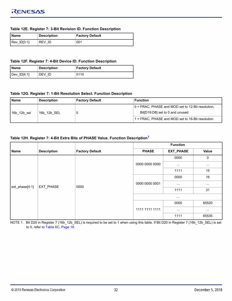
32©2018 Integrated Device Technology, Inc. December 5, 2018
8V97051 Datasheet
Table 12E. Register 7: 3-Bit Revision ID. Function Description
Name Description Factory Default
Rev_ID[3:1] REV_ID 001
Table 12F. Register 7: 4-Bit Device ID. Function Description
Name Description Factory Default
Dev_ID[4:1] DEV_ID 0110
Table 12G. Register 7: 1-Bit Resolution Select. Function Description
Name Description Factory Default Function
16b_12b_sel 16b_12b_SEL 0
0 = FRAC, PHASE and MOD set to 12-Bit resolution,
Bit[D19:D8] set to 0 and unused
1 = FRAC, PHASE and MOD set to 16-Bit resolution
Table 12H. Register 7: 4-Bit Extra Bits of PHASE Value. Function Description1
Name Description Factory Default
Function
PHASE EXT_PHASE Value
ext_phase[4:1] EXT_PHASE 0000
0000 0000 0000
0000 0
... ...
1111 15
0000 0000 0001
0000 16
... ...
1111 31
...
1111 1111 1111
0000 65520
... ...
1111 65535
NOTE 1. Bit D20 in Register 7 (16b_12b_SEL) is required to be set to 1 when using this table. If Bit D20 in Register 7 (16b_12b_SEL) is set to 0, refer to Table 6C, Page 18.

33©2018 Integrated Device Technology, Inc. December 5, 2018
8V97051 Datasheet
Table 12I. Register 7: 4-Bit Extra Bits of MOD Value. Function Description1
Name Description Factory Default
Function
MOD EXT_MOD Value
ext_mod[4:1] EXT_MOD 0000
0000 0000 0000
0000 Not Allowed
0001 Not Allowed
0010 2
... ...
1111 15
0000 0000 0001
0000 16
... ...
1111 31
...
1111 1111 1111
0000 65520
... ...
1111 65535
NOTE 1. Bit D20 in Register 7 (16b_12b_SEL) is required to be set to 1 when using this table. If Bit D20 in Register 7 (16b_12b_SEL) is set to 0, refer to Table 6D, Page 19.
Table 12J. Register 7: 4-Bit Extra Bits of FRAC Value. Function Description1
Name Description Factory Default
Function
FRAC EXT_FRAC Value
ext_fdiv[4:1] EXT_FRAC 0000
0000 0000 0000
0000 0
0001 1
... ...
1111 15
0000 0000 0001
0000 16
... ...
1111 31
...
1111 1111 1111
0000 65520
... ...
1111 65535
NOTE 1. Bit D20 in Register 7 (16b_12b_SEL) is required to be set to 1 when using this table. If Bit D20 in Register 7 (16b_12b_SEL) is set to 0, refer to Table 5C, Page 17.

34©2018 Integrated Device Technology, Inc. December 5, 2018
8V97051 Datasheet
Table 12K. Register 7: 1-Bit SCLKE. Function Description
Name Description Factory Default Function
Sclke SCLKE 1
0 = Output Data in a Read Cycle on a Rising Edge of SCLK
1 = Output Data in a Read Cycle on a Falling Edge of SCLK
Table 12L. Register 7: 1-Bit READBACK_ADDR. Function Description1
Name Description Function
Rd_Addr[3:1] READBACK_ADDR
000 = Register 0
001 = Register 1
010 = Register 2
011 = Register 3
100 = Register 4
101 = Register 5
110 = Register 6
111 = Register 7
NOTE 1. In order to Read a register, the user must write to Register 7 first and set the SPI_R_WN Bit to 1 (READ) and indicate the address of the register to read in the READBACK_ADDR Bit (Bits[D6:D4]).
Table 12M. Register 7: 1-Bit SPI_R_WN. Function Description1
Name Description Factory Default Function
SPI_R_WN SPI_R_WN 00 = WRITE
1 = READ
NOTE 1. Writing this bit to a ‘1’ will allow the user to read back the register selected in READBACK_ADDR on the next 32 SCLK cycle. This bit will revert back to ‘0’ once it is written with ‘1’ and will not retain the ‘1’ value.
Table 12N. Register 7: 3-Bit Control Bits. Function Description1
Name Description Function
CB[3:1] CONTROL BITS 111 = Register 7 is programmed
NOTE 1. The user has to set CB[3:1] to 111 in order to write to Register 7.

35©2018 Integrated Device Technology, Inc. December 5, 2018
8V97051 Datasheet
Absolute Maximum RatingsNOTE: Stresses beyond those listed under Absolute Maximum Ratings may cause permanent damage to the device. These ratings are stress specifications only. Functional operation of product at these conditions or any conditions beyond
those listed in the DC Characteristics or AC Characteristics is not implied. Exposure to absolute maximum rating conditions for extended periods may affect product reliability.
NOTE: VDDX denotes VDDD, V_CP, VDD_SD, VVCO.
Table 13. Absolute Maximum Ratings
Item Rating
Supply Voltage, VDDX 3.63V
Analog Supply Voltage, VDDA 3.63V
Input, VI
REF_IN
Other Inputs (MUTE, SDI, FLSW, VTUNE)
-0.5 to VDDA + 0.5V
Outputs, VO
RF_OUTA-B, nRF_OUTA-B-0.5 to VDDA + 0.5V
Outputs, VO (SCLK, LD, nCS, MUX_OUT) -0.5 to VDDA + 0.5V
Outputs, IO
Continuous Current
Surge Current
40mA
65mA
Outputs, IO (SCLK, LD, nCS, MUX_OUT)
Continuous Current
Surge Current
8mA
13mA
Junction Temperature, TJ 125°C
Storage Temperature, TSTG -65°C to 150°C
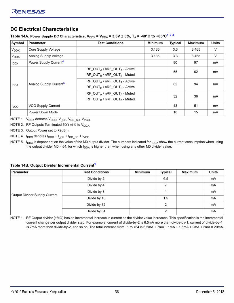
36©2018 Integrated Device Technology, Inc. December 5, 2018
8V97051 Datasheet
DC Electrical CharacteristicsTable 14A. Power Supply DC Characteristics, VDDX = VDDA = 3.3V ± 5%, TA = -40°C to +85°C 21 3
NOTE 1. VDDX denotes VDDD, V_CP, VDD_SD, VVCO.
NOTE 2. RF Outputs Terminated 50to VDDA.
NOTE 3. Output Power set to +2dBm.
Symbol Parameter Test Conditions Minimum Typical Maximum Units
VDDX Core Supply Voltage 3.135 3.3 3.465 V
VDDA Analog Supply Voltage 3.135 3.3 3.465 V
IDDX Power Supply Current4
NOTE 4. IDDX denotes IDDD + I_CP + IDD_SD + IVCO.
80 97 mA
IDDA Analog Supply Current5
NOTE 5. IDDA is dependent on the value of the M0 output divider. The numbers indicated for IDDA show the current consumption when using the output divider M0 = 64, for which IDDA is higher than when using any other M0 divider value.
RF_OUTA / nRF_OUTA - Active
RF_OUTB / nRF_OUTB - Muted55 62 mA
RF_OUTA / nRF_OUTA - Active
RF_OUTB / nRF_OUTB - Active82 94 mA
RF_OUTA / nRF_OUTA - Muted
RF_OUTB / nRF_OUTB - Muted32 36 mA
IVCO VCO Supply Current 43 51 mA
Power Down Mode 10 15 mA
Table 14B. Output Divider Incremental Current1
NOTE 1. RF Output divider (÷MO) has an incremental increase in current as the divider value increases. This specification is the incremental current change per output divider step. For example, current of divide-by-2 is 6.5mA more than divide-by-1, current of divide-by-4 is 7mA more than divide-by-2, and so on. The total increase from ÷1 to ÷64 is 6.5mA + 7mA + 1mA + 1.5mA + 2mA + 2mA = 20mA.
Parameter Test Conditions Minimum Typical Maximum Units
Output Divider Supply Current
Divide by 2 6.5 mA
Divide by 4 7 mA
Divide by 8 1 mA
Divide by 16 1.5 mA
Divide by 32 2 mA
Divide by 64 2 mA

37©2018 Integrated Device Technology, Inc. December 5, 2018
8V97051 Datasheet
Table 14C. Typical Current by Power Domain1
NOTE 1. Operating conditions are:REF_IN = 25MHzINT = 100 (integer mode)RF Divider = ÷1RF_OUTA = RF_OUTB = 2.5GHzRFPOWER = -1dBmCharge Pump = 0.31mA
Pin Name Pin Number Typical Current Unit
V_CP 6 24 mA
VVCO 16, 17 30 mA
VDDD 28 0.5 mA
VDD_SD 32 6 mA
VDDA 10 52 mA
Table 14D. LVCMOS DC Characteristics, VDDX = VDDA = 3.3V ± 5%, TA = -40°C to 85°C1
NOTE 1. VDDX denotes VDDD, V_CP, VDD_SD, VVCO.
Symbol Parameter Test Conditions Minimum Typical Maximum Units
VIH Input High VoltageMUTE, CE 1.8 VDDx V
SDI, SCLK, nCS 1.5 VDDx V
VIL Input Low Voltage -0.3 0.6 V
IIH Input High CurrentSDI, MUTE, CE VDDx = 3.465V, VIN = 1.8V 5 µA
SCLK, nCS VDDx = 3.465V, VIN = 1.8V 150 µA
IIL Input Low CurrentSDI, MUTE, CE VDDx = 3.465V, VIN = 0V -150 µA
SCLK, nCS VDDx = 3.465V, VIN = 0V -5 µA
VOH Output High Voltage MUX_OUT, LD VDDx = 3.465V; IOH = -500µA VDDX - 0.4 V
VOL Output Low Voltage MUX_OUT, LD VDDx = 3.465V; IOL = 500µA 0.4 V

38©2018 Integrated Device Technology, Inc. December 5, 2018
8V97051 Datasheet
AC Electrical Characteristics
Table 15A. AC Characteristics, VDDX = VDDA = 3.3V ± 5%, TA = -40°C to 85°C1
NOTE 1. VDDX denotes VDDD, V_CP, VDD_SD, VVCO.
Symbol Parameter Test Conditions Minimum Typical Maximum Units
REF_IN Input Reference Frequency2
NOTE 2. For REF_IN <10MHz, the slew rate must be >21V/µs.
Ref Doubler Disabled 5 310 MHz
Ref Doubler Enabled 5 100 MHz
VPP Input Sensitivity REF_IN Biased at VDDA/23
NOTE 3. AC-coupling the reference signal ensures VDDA/2 biasing.
0.7 VDDA V
fVCO VCO Frequency Fundamental VCO Mode 2200 4400 MHz
fRF_OUT Output Frequency Divider Values: 1, 2, 4, 8, 16, 32, 64 34.375 4400 MHz
fPFD PFD FrequencyFractional Mode 125 MHz
Integer Mode 310 MHz
KVCO VCO Sensitivity 40 MHz/V
tLOCK PLL Lock TimeTime from Low to High nCS until
Low to High LD1 ms
- Output Power Variation ±1 dB
- RF Output Power Muted 80 dBm
- Min/Max VCO Tuning Voltage 0.5 / 2.5 V

39©2018 Integrated Device Technology, Inc. December 5, 2018
8V97051 Datasheet
Table 15B. RF_OUT[A:B] Phase Noise and Jitter Characteristics, VDDX = VDDA = 3.3V ± 5%, TA = -40°C to 85°C1 2
Symbol Parameter Test Conditions Minimum Typical Maximum Units
tjit(Ø) RMS Phase Jitter (Random)
f = 156.25MHzIntegration Range: 12kHz - 20MHz
149 fs
f = 2.05GHzIntegration Range: 12kHz - 20MHz
147 fs
f = 1.76GHzIntegration Range: 12kHz - 20MHz
126 fs
N(100k)
RF OutputPhase Noise Performance@ 1.1GHz (Open Loop)
100kHz Offset from Carrier -118.4 dBc/Hz
N(800k) 800kHz Offset from Carrier -141 dBc/Hz
N(1M) 1MHz Offset from Carrier -143 dBc/Hz
N(5M) 5MHz Offset from Carrier -152.4 dBc/Hz
N(10M) 10MHz Offset from Carrier -154 dBc/Hz
N() Noise Floor (30MHz from Carrier) -154 dBc/Hz
N(100k)
RF OutputPhase Noise Performance@ 1.65GHz (Open Loop)
100kHz Offset from Carrier -112.2 dBc/Hz
N(800k) 800kHz Offset from Carrier -136.9 dBc/Hz
N(1M) 1MHz Offset from Carrier -139.2 dBc/Hz
N(5M) 5MHz Offset from Carrier -151.2 dBc/Hz
N(10M) 10MHz Offset from Carrier -153.1 dBc/Hz
N() Noise Floor (30MHz from Carrier) -154.4 dBc/Hz
N(100k)
RF OutputPhase Noise Performance@ 2.3GHz (Open Loop)
100kHz Offset from Carrier -112.1 dBc/Hz
N(800k) 800kHz Offset from Carrier -135.7 dBc/Hz
N(1M) 1MHz Offset from Carrier -137.8 dBc/Hz
N(5M) 5MHz Offset from Carrier -150.8 dBc/Hz
N(10M) 10MHz Offset from Carrier -153.8 dBc/Hz
N() Noise Floor (30MHz from Carrier) -155.1 dBc/Hz
N(100k)
RF OutputPhase Noise Performance@ 3.8GHz (Open Loop)
100kHz Offset from Carrier -106 dBc/Hz
N(800k) 800kHz Offset from Carrier -130.9 dBc/Hz
N(1M) 1MHz Offset from Carrier -133.2 dBc/Hz
N(5M) 5MHz Offset from Carrier -148.1 dBc/Hz
N(10M) 10MHz Offset from Carrier -152.2 dBc/Hz
N() Noise Floor (30MHz from Carrier) -154.7 dBc/Hz
N(100k)
RF OutputPhase Noise Performance@ 4.4GHz (Open Loop)
100kHz Offset from Carrier -102 dBc/Hz
N(800k) 800kHz Offset from Carrier -127 dBc/Hz
N(1M) 1MHz Offset from Carrier -129.5 dBc/Hz
N(5M) 5MHz Offset from Carrier -146 dBc/Hz
N(10M) 10MHz Offset from Carrier -150.5 dBc/Hz
N() Noise Floor (30MHz from Carrier) -153 dBc/Hz
-Spurious SignalsDue to PFD Frequency
fPFD = 50MHz;RF_OUTA = 2.2GHz
-74 dBc
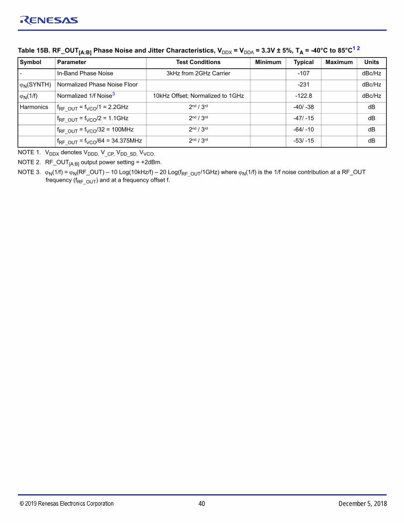
40©2018 Integrated Device Technology, Inc. December 5, 2018
8V97051 Datasheet
Symbol Parameter Test Conditions Minimum Typical Maximum Units
- In-Band Phase Noise 3kHz from 2GHz Carrier -107 dBc/Hz
N(SYNTH) Normalized Phase Noise Floor -231 dBc/Hz
N(1/f) Normalized 1/f Noise3 10kHz Offset; Normalized to 1GHz -122.8 dBc/Hz
Harmonics fRF_OUT = fVCO/1 = 2.2GHz 2nd / 3rd -40/ -38 dB
fRF_OUT = fVCO/2 = 1.1GHz 2nd / 3rd -47/ -15 dB
fRF_OUT = fVCO/32 = 100MHz 2nd / 3rd -64/ -10 dB
fRF_OUT = fVCO/64 = 34.375MHz 2nd / 3rd -53/ -15 dB
NOTE 1. VDDX denotes VDDD, V_CP, VDD_SD, VVCO.
NOTE 2. RF_OUT[A:B] output power setting = +2dBm.
NOTE 3. N(1/f) = N(RF_OUT) – 10 Log(10kHz/f) – 20 Log(fRF_OUT/1GHz) where N(1/f) is the 1/f noise contribution at a RF_OUT frequency (fRF_OUT) and at a frequency offset f.
Table 15B. RF_OUT[A:B] Phase Noise and Jitter Characteristics, VDDX = VDDA = 3.3V ± 5%, TA = -40°C to 85°C1 2

41©2018 Integrated Device Technology, Inc. December 5, 2018
8V97051 Datasheet
Phase Noise at 156.25MHz (3.3V)
Phase Noise at 1.76GHz (3.3V)
Noi
se P
ow
erdB
cH
z
Offset Frequency (Hz)
Noi
se P
ower
dBc
Hz
Offset Frequency (Hz)
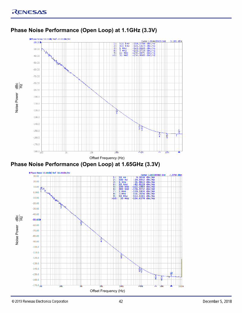
42©2018 Integrated Device Technology, Inc. December 5, 2018
8V97051 Datasheet
Phase Noise Performance (Open Loop) at 1.1GHz (3.3V)
Phase Noise Performance (Open Loop) at 1.65GHz (3.3V)
Noi
se P
ower
dBc
Hz
Offset Frequency (Hz)
Noi
se P
owe
rdB
cH
z
Offset Frequency (Hz)
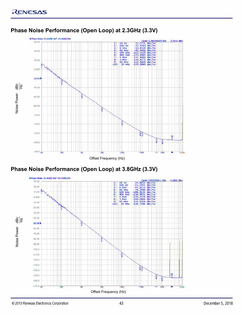
43©2018 Integrated Device Technology, Inc. December 5, 2018
8V97051 Datasheet
Phase Noise Performance (Open Loop) at 2.3GHz (3.3V)
Phase Noise Performance (Open Loop) at 3.8GHz (3.3V)
Noi
se P
ower
dBc
Hz
Offset Frequency (Hz)
Noi
se P
ower
dBc
Hz
Offset Frequency (Hz)

44©2018 Integrated Device Technology, Inc. December 5, 2018
8V97051 Datasheet
Applications Information
Loop Filter Calculations
2nd Order Loop Filter
This section helps design a 2nd order loop filter for the 8V97051. A general 2nd order loop filter is shown in Figure 11, Typical 2nd Order Loop Filter. Step-by-step calculations to determine Rz, Cz, and Cp values for a desired loop bandwidth are described below. Required parameters are provided. A spreadsheet for calculating the loop filter values is also available.
Figure 11. Typical 2nd Order Loop Filter
1. Determine desired loop bandwidth fc.
2. Calculate Rz:
Where,
Icp is charge pump current. Icp is programmable from 310µA to 5mA.
N is effective feedback divider. N must be programmed into the following value.
FVCO is VCO frequency. VCO frequency range: 2200MHz to 4400MHz
Fpd is phase detector input frequency.
F_ref is reference clock (REF_IN) input frequency.
Pv is overall pre-divider setting.
Kvco is VCO gain. Kvco = 40MHz/V
3. Calculate Cz:
Where,
= fc/ fz, user can determine an number. > 6 is recommended.
fz is frequency at zero.
4. Calculate Cp:
Where,
= fp/fc, user can determine number. > 4 is recommended.
fp is frequency at pole.
5. Verify Phase Margin (PM)
Where,
The phase margin (PM) should be greater than 50°.
A spreadsheet for calculating the loop filter component values is available at www.IDT.com. To use the spreadsheet, the user simply enters the following parameters:
fc, F_ref, PV, Icp, FVCO, and .
The spreadsheet will provide the component values, Rz, Cz and Cp as the result. The spreadsheet also calculates the maximum phase margin for verification.
RZ
CZ
Cp
KvcoIcp
NfcRz
*
***2
Fpd
FvcoN
Pv
refFFpd
_
RzfcCz
***2
*
CzCp
Cp
Czb 1

45©2018 Integrated Device Technology, Inc. December 5, 2018
8V97051 Datasheet
3rd Order Loop Filter
This section helps design a 3rd order loop filter for the 8V97051. A general 3rd order loop filter is shown in Figure 12, Typical 3rd Order Loop Filter.
Figure 12. Typical 3rd Order Loop Filter
The Rz, Cz and Cp can be calculated as 2nd order loop filter. The following equation help determine the 3rd order loop filter Rp2 and Cp2.
Pick an Rp2 value. Rp2 ~ 1.5xRz is suggested.
Where,
is ratio between the 1st pole frequency and the 2nd pole frequency. > 4 is recommended.
Recommendations for Unused Input and Output Pins
Inputs:
LVCMOS Control Pins
All control pins have internal pullup and pulldown resistors; additional resistance is not required but can be added for additional protection. A 1k resistor can be used.
Outputs:
Output Pins
For any unused output, it can be left floating and disabled.
Rz
Cz
Cp
Rp2
Cp2
RP2
CP2CP
RZ
CZ

46©2018 Integrated Device Technology, Inc. December 5, 2018
8V97051 Datasheet
Schematic ExampleFigure 13A and Figure 13B show general application schematic examples for the 8V97051.
For power rails, bypass capacitors must be provided to all power supply pins. Suggest at least one bypass capacitor per power pin. Value can be ranged from 0.01uF or 0.1uF. Mix values of bypass capacitor can help filtering wider range of power supply noise.
The 8V97051 input is high impedance. The input termination depends on the driver type termination requirements. In these examples, the 8V97051 REF_IN input is terminated with a matched load termination. For transmission line with characteristic impedance Zo = 50, the termination resistor R8 is 50. The input is self biased to proper DC offset after the AC coupling.
The loop filter values can be calculated to meet the loop bandwidth requirement. Please refer to the section, "Loop Filter Calculations" for detailed calculations. For fast lock mode, the loop filter can be configured as Fast Lock Loop Filter Option 1 or Fast Lock Loop Filter Option 2 shown in Figure 13A.
Fast Lock Loop Filter Option 1 is Parallel Resistor Configuration. For normal operating mode, only R5 is active and R5 = Rs, where Rs is the resistor value for normal operating mode loop bandwidth. In fast lock mode, the combination of R4 in parallel with R5 is active. For example, in normal operation mode, if the charge pump current is set at 0000 (ICP = 310uA), then, in fast lock mode, the loop bandwidth is set larger by increasing the charge pump current to ICP~5mA (ICP
setting = 1111 or 16 times the normal charge pump current). The combination of the R4 and R5 in parallel is 1/4 * Rs.
Fast Lock Loop Filter Option 2 is Series Resistor Configuration. For normal operating mode, both R6 and R7 are active and R6 + R7 = Rs. For fast lock mode, only R6 is active. For example, in normal operation mode, if the charge pump current is set at 0000 (ICP = 310uA), then, in fast lock mode, the loop bandwidth is set larger by increasing the charge pump current to ICP~5mA (ICP setting = 1111 or 16 times the normal charge pump current). The sum of R6 and R7 equals to Rs, i.e. R6 + R7 = Rs. R6 = 1/4 * Rs and R7 = 3/4 * Rs.
The 8V97051 output pull-up loading can be resistors or inductors. The pull up resistor value is typically 50. Resistor pull up loading covers wide range of output frequencies. For inductor pull up loading, the inductor value is frequency dependent. One inductor value cannot cover all the output frequency range. This example shows the L = 3.9nH that is suitable for approximately 2GHz operating frequency. The output can also drive single ended LO input. Figure 13B shows an example of the 8V97051 output driving single ended LO input of the mixer through an LC balun. The LC balun component values are frequency dependent. These values can be adjusted to optimize the performance. Single ended LO receiver input also can tap to one side of the differential driver using resistor loading or inductor loading. For single ended LO input, both sides of the differential driver still need to be loaded with pull up. The output power level can also be adjusted further through programming.

47©2018 Integrated Device Technology, Inc. December 5, 2018
8V97051 Datasheet
Figure 13A. An 8V97051 General Application Schematic Example
U1
SCLK
1
SDI
2
nCS
3
CE
4
FLSW
5
V_C
P6
CP_
OU
T7
GN
D_C
P8
GNDA9VDDA10GNDA_VCO11RF_OUTA12nRF_OUTA13RF_OUTB14nRF_OUTB15VVCO16
VVC
O17
GN
DA_
VCO
18VB
IAS
19VT
UN
E20
GN
DA_
VCO
21R
CP
22VC
OM
23VR
EF24
VDD_SD32 GND_SD31 MUX_OUT30 REF_IN29 VDDD28 GNDD27 MUTE26 LD25
33 E_PAD
C11
C12R5
R3
CP_OUT
C13
nREF_OUTA
VDD
V_v co
VTU
NE
VTUNE
VDD
VDD
R14.7k
VDD
C81n
C71n
L13.9n
L23.9n
C1
10u
C2
0.1uC4
0.1u
C5
10u
FLSW
C3
0.1u
C6
1u
nREF_OUTA
SPI Compatible Serial Bus
REF_OUTA
Resistor Loading
All power supply pins require Bypass capacitors
Inductor Loading
C11
C12R5
R3CP_OUT
C13
FLSW
VTUNE
R4
R250
R150
C9 1n
C101n
RF MixerZo = 50
Zo = 50
LO input
Zdiff=100
VDD
Fast Lock Loop Filter Options 1
Loop Filterwithout Fast Lock
C11
C12
CP_OUT
R7
R3
C13
FLSW
VTUNE
R6
Fast Lock Loop Filter Options 2
REF_OUTA
R850
RF IN

48©2018 Integrated Device Technology, Inc. December 5, 2018
8V97051 Datasheet
Figure 13B. Schematic Example for Driving Single Ended Mixer
L3
C14
C15
C11
C9
C12R5
R3
C13
VDD
V_v co
VTU
NE
VTUNE
VDD
VDD
VDD
R14.7k
C81n
C71n
C1
10u
C2
0.1uC4
0.1u
C5
10u
R4
Optional
U1
SCLK
1
SDI
2
nCS
3
CE
4
FLSW
5
V_C
P6
CP_
OU
T7
GN
D_C
P8
GNDA9VDDA10GNDA_VCO11RF_OUTA12nRF_OUTA13RF_OUTB14nRF_OUTB15VVCO16
VVC
O17
GN
DA_
VCO
18VB
IAS
19VT
UN
E20
GN
DA_
VCO
21R
CP
22VC
OM
23VR
EF24
VDD_SD32 GND_SD31 MUX_OUT30 REF_IN29 VDDD28 GNDD27 MUTE26 LD25
33 E_PAD
C3
0.1u
C6
1u
SPI Compatible Serial Bus
All power supply pins require Bypass capacitors
Zo = 50LO input
R850
R250
R150
L13.9n
L23.9n
L1L2
IDT F1102
IDT F1100
IDT F1152
IDT F1150
IDT F1178
IDT F1160
RF to IF Dual Downconverter Mixer
RF IN
RFin_A
RFin_B
IFout_A
IFout_B
VDD
Inductor Loading
REF_OUTA
nREF_OUTA
VDD
REF_OUTA
nREF_OUTAC9
C9
Resistor Loading
49©2018 Integrated Device Technology, Inc. December 5, 2018
8V97051 Datasheet
Power ConsiderationsThe 8V97051 device was designed and characterized to operate within the ambient industrial temperature range of -40°C to +85°C. The ambient temperature represents the temperature around the device, not the junction temperature. When using the device in extreme cases, such as maximum operating frequency and high ambient temperature, external air flow may be required in order to ensure a safe and reliable junction temperature. Extreme care must be taken to avoid exceeding 125°C junction temperature. The power calculation example below was generated using a typical configuration. For many applications, the power consumption can vary depending on configuration. Please contact IDT technical support for any concerns on calculating the power dissipation for your own specific configuration.
1. Power Dissipation.
The total power dissipation for the 8V97051 is the sum of the core power plus the power dissipation in the output driver. The following is the power dissipation for VDD = 3.465V, which gives worse case results.
• Power (core)MAX = VDD_MAX * (IDDA + IVCO + ICP + IDD_SD + IDDD)MAX = VDD_MAX * (IDDA + IDDX)MAX = 3.465V * (94mA + 97mA) = 661.8mW
Total Power (with two outputs active at 2dBm output power level) = 661.8mW
2. Junction Temperature.
Junction temperature, Tj, is the temperature at the junction of the bond wire and bond pad, and directly affects the reliability of the device. The maximum recommended junction temperature is 125°C. Limiting the internal transistor junction temperature, Tj, to 125°C ensures that the bond wire and bond pad temperature remains below 125°C.
The equation for Tj is as follows: Tj = JA * Pd_total + TA
Tj = Junction Temperature
JA = Junction-to-Ambient Thermal Resistance
Pd_total = Total Device Power Dissipation (example calculation is in section 1 above)
TA = Ambient Temperature
In order to calculate junction temperature, the appropriate junction-to-ambient thermal resistance JA must be used. Assuming no air flow and a multi-layer board, the appropriate value is 34.34°C/W per Table 16 below.
Therefore, Tj for an ambient temperature of 85°C with all outputs active is:
85°C + 0.662W * 34.34°C/W = 107.7°C. This is below the limit of 125°C.
This calculation is only an example. Tj will obviously vary depending on the number of loaded outputs, supply voltage, air flow and the type of board (multi-layer).
Table 16. Thermal Resistance JA for 32 Lead VFQFN, Forced Convection
Meters per Second 0 1 2
Multi-Layer PCB, JEDEC Standard Test Boards
JA by Velocity
34.34°C/W 30.7°C/W 29.12°C/W
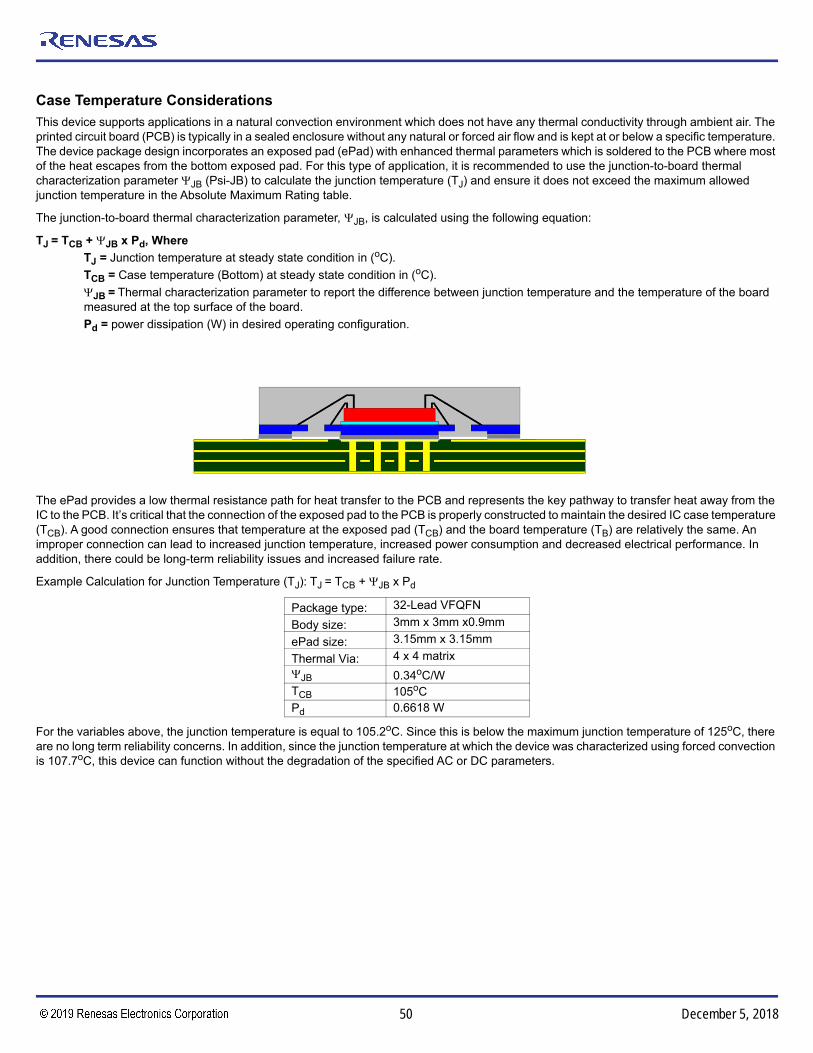
50©2018 Integrated Device Technology, Inc. December 5, 2018
8V97051 Datasheet
Case Temperature Considerations
This device supports applications in a natural convection environment which does not have any thermal conductivity through ambient air. The printed circuit board (PCB) is typically in a sealed enclosure without any natural or forced air flow and is kept at or below a specific temperature. The device package design incorporates an exposed pad (ePad) with enhanced thermal parameters which is soldered to the PCB where most of the heat escapes from the bottom exposed pad. For this type of application, it is recommended to use the junction-to-board thermal characterization parameter JB (Psi-JB) to calculate the junction temperature (TJ) and ensure it does not exceed the maximum allowed junction temperature in the Absolute Maximum Rating table.
The junction-to-board thermal characterization parameter, JB, is calculated using the following equation:
TJ = TCB + JB x Pd, Where
TJ = Junction temperature at steady state condition in (oC).
TCB = Case temperature (Bottom) at steady state condition in (oC).
JB = Thermal characterization parameter to report the difference between junction temperature and the temperature of the board measured at the top surface of the board.
Pd = power dissipation (W) in desired operating configuration.
The ePad provides a low thermal resistance path for heat transfer to the PCB and represents the key pathway to transfer heat away from the IC to the PCB. It’s critical that the connection of the exposed pad to the PCB is properly constructed to maintain the desired IC case temperature (TCB). A good connection ensures that temperature at the exposed pad (TCB) and the board temperature (TB) are relatively the same. An improper connection can lead to increased junction temperature, increased power consumption and decreased electrical performance. In addition, there could be long-term reliability issues and increased failure rate.
Example Calculation for Junction Temperature (TJ): TJ = TCB + JB x Pd
For the variables above, the junction temperature is equal to 105.2oC. Since this is below the maximum junction temperature of 125oC, there are no long term reliability concerns. In addition, since the junction temperature at which the device was characterized using forced convection is 107.7oC, this device can function without the degradation of the specified AC or DC parameters.
Package type: 32-Lead VFQFN
Body size: 3mm x 3mm x0.9mm
ePad size: 3.15mm x 3.15mm
Thermal Via: 4 x 4 matrix
JB 0.34oC/WTCB 105oCPd 0.6618 W

51©2018 Integrated Device Technology, Inc. December 5, 2018
8V97051 Datasheet
Reliability InformationTable 17A. JA vs. Air Flow Table for a 32 lead VFQFN
Table 17B. JB vs. Air Flow Table for a 32 lead VFQFN
NOTE: JB is independent of airflow.
Transistor CountThe 8V97051 transistor count is: 409,546
Package Outline DrawingsThe package outline drawings are appended at the end of this document and are accessible from the link below. The package information is the most current data available.
www.idt.com/document/psc/32-vfqfpn-package-outline-drawing-50-x-50-x-090-mm-body-epad-315-x-315-mm-nlg32p1
JA vs. Air Flow
Meters per Second 0 1 2
Multi-Layer PCB, JEDEC Standard Test Boards 34.34°C/W 30.7°C/W 29.12°C/W
JB vs. Air Flow
Meters per Second 0
Multi-Layer PCB, JEDEC Standard Test Boards 0.472°C/W
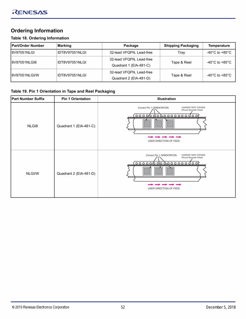
52©2018 Integrated Device Technology, Inc. December 5, 2018
8V97051 Datasheet
Ordering InformationTable 18. Ordering Information
Part/Order Number Marking Package Shipping Packaging Temperature
8V97051NLGI IDT8V97051NLGI 32-lead VFQFN, Lead-free Tray -40°C to +85°C
8V97051NLGI8 IDT8V97051NLGI32-lead VFQFN, Lead-free
Quadrant 1 (EIA-481-C)Tape & Reel -40°C to +85°C
8V97051NLGI/W IDT8V97051NLGI32-lead VFQFN, Lead-free
Quadrant 2 (EIA-481-D)Tape & Reel -40°C to +85°C
Table 19. Pin 1 Orientation in Tape and Reel Packaging
Part Number Suffix Pin 1 Orientation Illustration
NLGI8 Quadrant 1 (EIA-481-C)
NLGI/W Quadrant 2 (EIA-481-D)
USER DIRECTION OF FEED
Correct Pin 1 ORIENTATION CARRIER TAPE TOPSIDE(Round Sprocket Holes)
USER DIRECTION OF FEED
Correct Pin 1 ORIENTATION CARRIER TAPE TOPSIDE(Round Sprocket Holes)
8V97051 Datasheet
DISCLAIMER Integrated Device Technology, Inc. (IDT) and its affiliated companies (herein referred to as “IDT”) reserve the right to modify the products and/or specifications described herein at any time, without notice, at IDT’s sole discretion. Performance specifications and operating parameters of the described products are determined in an independent state and are not guaranteed to perform the same way when installed in customer products. The information contained herein is provided without representation or warranty of any kind, whether express or implied, including, but not limited to, the suitability of IDT's products for any particular purpose, an implied warranty of merchantability, or non-infringement of the intellectual property rights of others. This document is presented only as a guide and does not convey any license under intellectual property rights of IDT or any third parties.
IDT's products are not intended for use in applications involving extreme environmental conditions or in life support systems or similar devices where the failure or malfunction of an IDT product can be reasonably expected to significantly affect the health or safety of users. Anyone using an IDT product in such a manner does so at their own risk, absent an express, written agreement by IDT.
Integrated Device Technology, IDT and the IDT logo are trademarks or registered trademarks of IDT and its subsidiaries in the United States and other countries. Other trademarks used herein are the property of IDT or their respective third party owners. For datasheet type definitions and a glossary of common terms, visit www.idt.com/go/glossary. Integrated Device Technology, Inc. All rights reserved.
Tech Supportwww.IDT.com/go/support
Sales1-800-345-7015 or 408-284-8200 Fax: 408-284-2775www.IDT.com/go/sales
Corporate Headquarters6024 Silver Creek Valley Road San Jose, CA 95138 USAwww.IDT.com
53©2018 Integrated Device Technology, Inc. December 5, 2018
Revision History
Revision Date Description of Change
December 5, 2019* Added the sentence starting with "For optimal performance...” to Integrated Low Noise VCO. This informationwas inadvertently removed from the datasheet during the previous release.
August 8, 2018
* Removed the sentence starting with “For optimal performance...” from Integrated Low Noise VCO
* Changed incorrect measurement unit nF to nH in Output Matching and Schematic Example
* Updated the Package Outline Drawings; however, no mechanical changes
November 19, 2017* Updated Note 3 in Table 15B
* Completed other minor changes
February 10, 2017
* Integrated Low Noise VCO - added sentence
* Updated Package Outline Drawings
* Ordering Information - updated table package column
* Updated datasheet footer
September 22, 2016
* Description update
* Updated schematic examples
* Updated datasheet header/footers
July 30, 2015* Features - added case temperature bullet
* Added case temperature consideration section
June 30, 2015 * Power Considerations - corrected Power Dissipation section and Tj equation

© Integrated Device Technology, Inc.
32-VFQFPN, Package Outline Drawing
5.0 x 5.0 x 0.90 mm Body, Epad 3.15 x 3.15 mm.NLG32P1, PSC-4171-01, Rev 02, Page 1

© Integrated Device Technology, Inc.
32-VFQFPN, Package Outline Drawing
5.0 x 5.0 x 0.90 mm Body, Epad 3.15 x 3.15 mm.NLG32P1, PSC-4171-01, Rev 02, Page 2
Package Revision HistoryRev No.Date Created Description
Feb 8, 2016 Rev 01 Added "k: ValueApril 12, 2018 Rev 02 New Format
Corporate HeadquartersTOYOSU FORESIA, 3-2-24 Toyosu,Koto-ku, Tokyo 135-0061, Japanwww.renesas.com
Contact InformationFor further information on a product, technology, the most up-to-date version of a document, or your nearest sales office, please visit:www.renesas.com/contact/
TrademarksRenesas and the Renesas logo are trademarks of Renesas Electronics Corporation. All trademarks and registered trademarks are the property of their respective owners.
IMPORTANT NOTICE AND DISCLAIMER
RENESAS ELECTRONICS CORPORATION AND ITS SUBSIDIARIES (“RENESAS”) PROVIDES TECHNICAL SPECIFICATIONS AND RELIABILITY DATA (INCLUDING DATASHEETS), DESIGN RESOURCES (INCLUDING REFERENCE DESIGNS), APPLICATION OR OTHER DESIGN ADVICE, WEB TOOLS, SAFETY INFORMATION, AND OTHER RESOURCES “AS IS” AND WITH ALL FAULTS, AND DISCLAIMS ALL WARRANTIES, EXPRESS OR IMPLIED, INCLUDING, WITHOUT LIMITATION, ANY IMPLIED WARRANTIES OF MERCHANTABILITY, FITNESS FOR A PARTICULAR PURPOSE, OR NON-INFRINGEMENT OF THIRD PARTY INTELLECTUAL PROPERTY RIGHTS.
These resources are intended for developers skilled in the art designing with Renesas products. You are solely responsible for (1) selecting the appropriate products for your application, (2) designing, validating, and testing your application, and (3) ensuring your application meets applicable standards, and any other safety, security, or other requirements. These resources are subject to change without notice. Renesas grants you permission to use these resources only for development of an application that uses Renesas products. Other reproduction or use of these resources is strictly prohibited. No license is granted to any other Renesas intellectual property or to any third party intellectual property. Renesas disclaims responsibility for, and you will fully indemnify Renesas and its representatives against, any claims, damages, costs, losses, or liabilities arising out of your use of these resources. Renesas' products are provided only subject to Renesas' Terms and Conditions of Sale or other applicable terms agreed to in writing. No use of any Renesas resources expands or otherwise alters any applicable warranties or warranty disclaimers for these products.
(Rev.1.0 Mar 2020)
© 2020 Renesas Electronics Corporation. All rights reserved.