Low Power VLSI Circuits and Systems Prof. Ajit Pal...
20
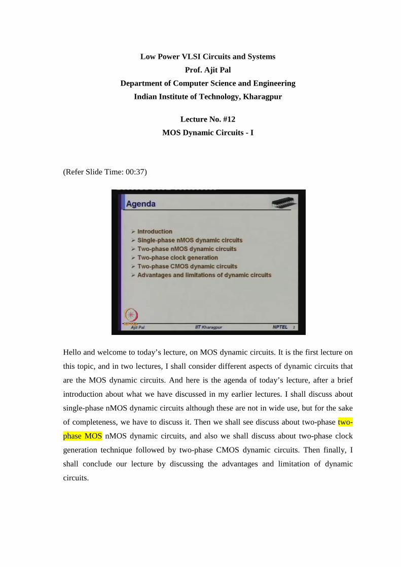
Low Power VLSI Circuits and Systems Prof. Ajit Pal Department of Computer Science and Engineering Indian Institute of Technology, Kharagpur Lecture No. #12 MOS Dynamic Circuits - I (Refer Slide Time: 00:37) Hello and welcome to today’s lecture, on MOS dynamic circuits. It is the first lecture on this topic, and in two lectures, I shall consider different aspects of dynamic circuits that are the MOS dynamic circuits. And here is the agenda of today’s lecture, after a brief introduction about what we have discussed in my earlier lectures. I shall discuss about single-phase nMOS dynamic circuits although these are not in wide use, but for the sake of completeness, we have to discuss it. Then we shall see discuss about two-phase two- phase MOS nMOS dynamic circuits, and also we shall discuss about two-phase clock generation technique followed by two-phase CMOS dynamic circuits. Then finally, I shall conclude our lecture by discussing the advantages and limitation of dynamic circuits.
Transcript of Low Power VLSI Circuits and Systems Prof. Ajit Pal...
Low Power VLSI Circuits and Systems Prof. Ajit Pal
Department of Computer Science and Engineering Indian Institute of Technology, Kharagpur
Lecture No. #12
MOS Dynamic Circuits - I
(Refer Slide Time: 00:37)
Hello and welcome to today’s lecture, on MOS dynamic circuits. It is the first lecture on
this topic, and in two lectures, I shall consider different aspects of dynamic circuits that
are the MOS dynamic circuits. And here is the agenda of today’s lecture, after a brief
introduction about what we have discussed in my earlier lectures. I shall discuss about
single-phase nMOS dynamic circuits although these are not in wide use, but for the sake
of completeness, we have to discuss it. Then we shall see discuss about two-phase two-
phase MOS nMOS dynamic circuits, and also we shall discuss about two-phase clock
generation technique followed by two-phase CMOS dynamic circuits. Then finally, I
shall conclude our lecture by discussing the advantages and limitation of dynamic
circuits.
(Refer Slide Time: 01:22)
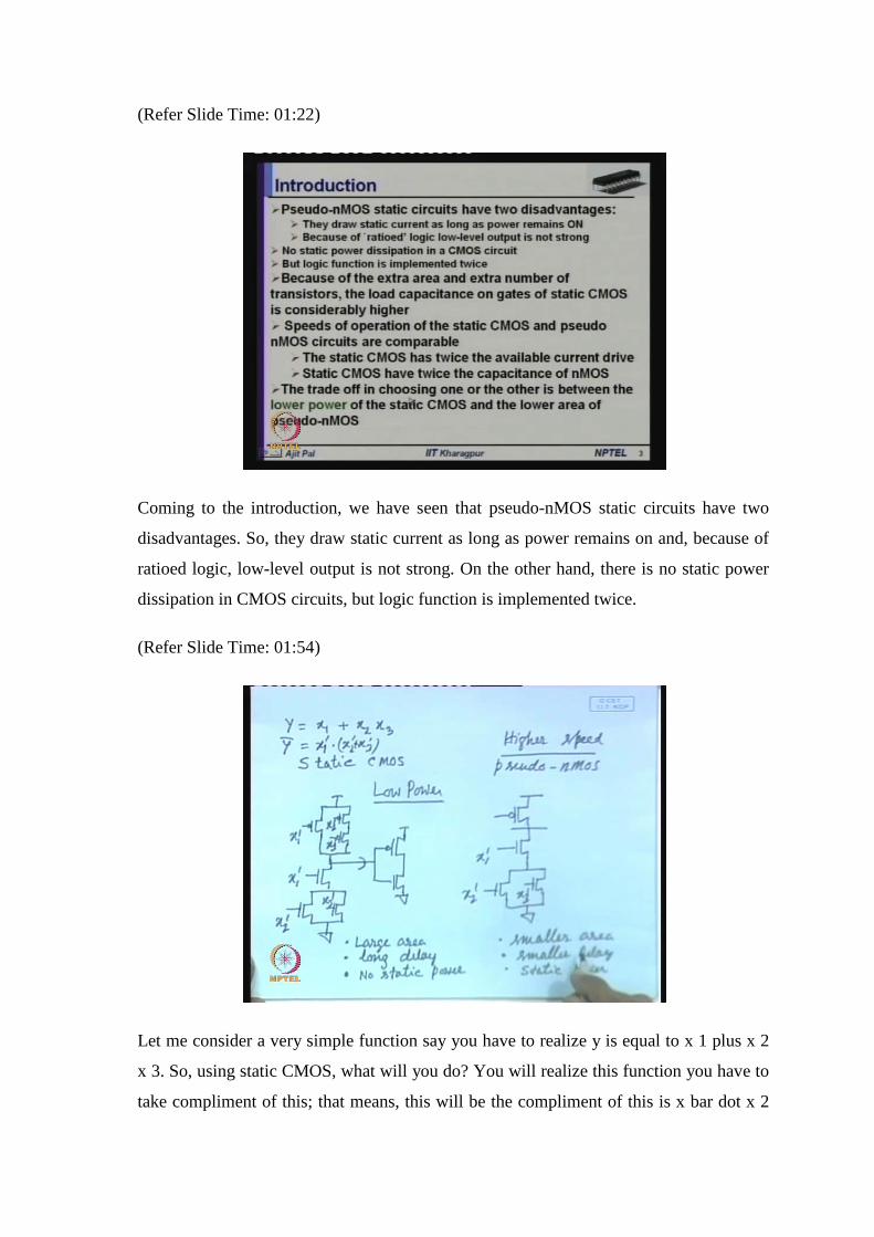
Coming to the introduction, we have seen that pseudo-nMOS static circuits have two
disadvantages. So, they draw static current as long as power remains on and, because of
ratioed logic, low-level output is not strong. On the other hand, there is no static power
dissipation in CMOS circuits, but logic function is implemented twice.
(Refer Slide Time: 01:54)
Let me consider a very simple function say you have to realize y is equal to x 1 plus x 2
x 3. So, using static CMOS, what will you do? You will realize this function you have to
take compliment of this; that means, this will be the compliment of this is x bar dot x 2
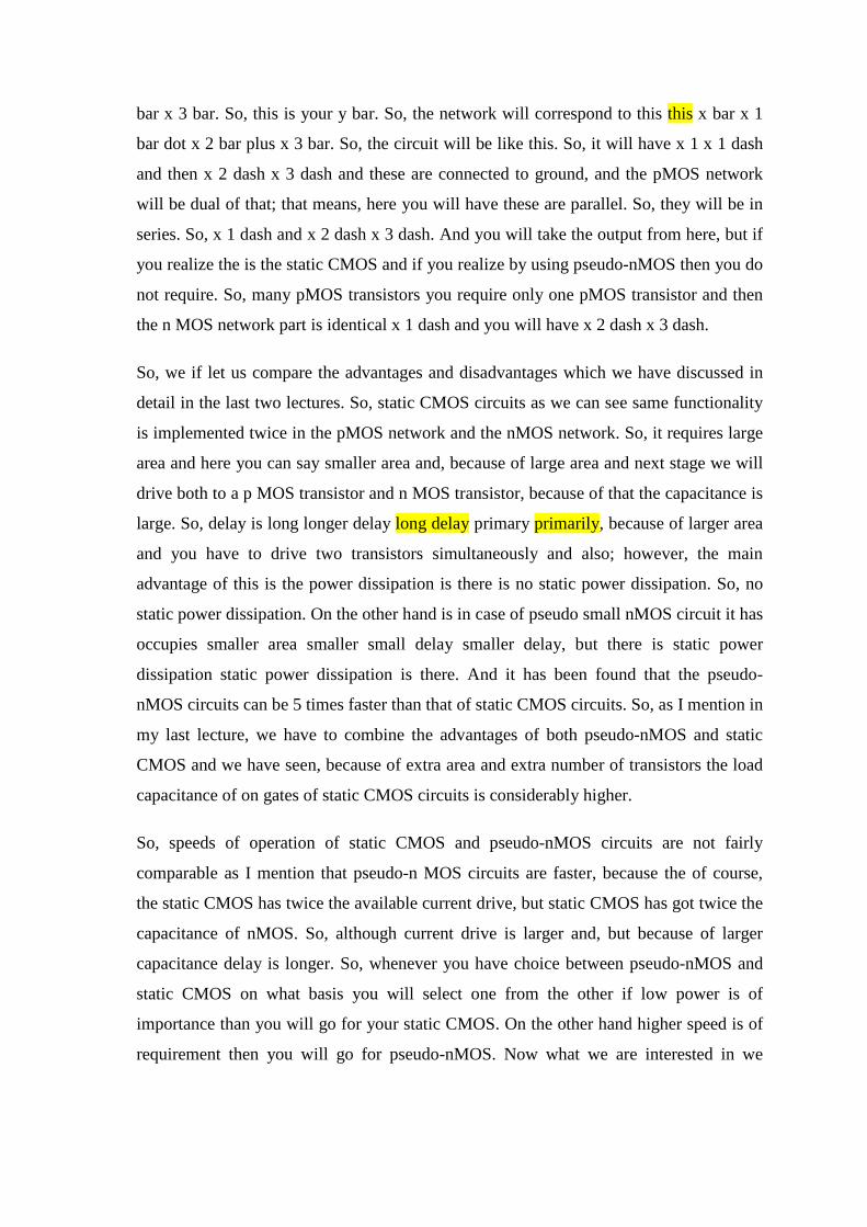
bar x 3 bar. So, this is your y bar. So, the network will correspond to this this x bar x 1
bar dot x 2 bar plus x 3 bar. So, the circuit will be like this. So, it will have x 1 x 1 dash
and then x 2 dash x 3 dash and these are connected to ground, and the pMOS network
will be dual of that; that means, here you will have these are parallel. So, they will be in
series. So, x 1 dash and x 2 dash x 3 dash. And you will take the output from here, but if
you realize the is the static CMOS and if you realize by using pseudo-nMOS then you do
not require. So, many pMOS transistors you require only one pMOS transistor and then
the n MOS network part is identical x 1 dash and you will have x 2 dash x 3 dash.
So, we if let us compare the advantages and disadvantages which we have discussed in
detail in the last two lectures. So, static CMOS circuits as we can see same functionality
is implemented twice in the pMOS network and the nMOS network. So, it requires large
area and here you can say smaller area and, because of large area and next stage we will
drive both to a p MOS transistor and n MOS transistor, because of that the capacitance is
large. So, delay is long longer delay long delay primary primarily, because of larger area
and you have to drive two transistors simultaneously and also; however, the main
advantage of this is the power dissipation is there is no static power dissipation. So, no
static power dissipation. On the other hand is in case of pseudo small nMOS circuit it has
occupies smaller area smaller small delay smaller delay, but there is static power
dissipation static power dissipation is there. And it has been found that the pseudo-
nMOS circuits can be 5 times faster than that of static CMOS circuits. So, as I mention in
my last lecture, we have to combine the advantages of both pseudo-nMOS and static
CMOS and we have seen, because of extra area and extra number of transistors the load
capacitance of on gates of static CMOS circuits is considerably higher.
So, speeds of operation of static CMOS and pseudo-nMOS circuits are not fairly
comparable as I mention that pseudo-n MOS circuits are faster, because the of course,
the static CMOS has twice the available current drive, but static CMOS has got twice the
capacitance of nMOS. So, although current drive is larger and, but because of larger
capacitance delay is longer. So, whenever you have choice between pseudo-nMOS and
static CMOS on what basis you will select one from the other if low power is of
importance than you will go for your static CMOS. On the other hand higher speed is of
requirement then you will go for pseudo-nMOS. Now what we are interested in we
would like to combine the advantages of both of them, and that is why as I mentioned in
my last lecture.
(Refer Slide Time: 07:31)
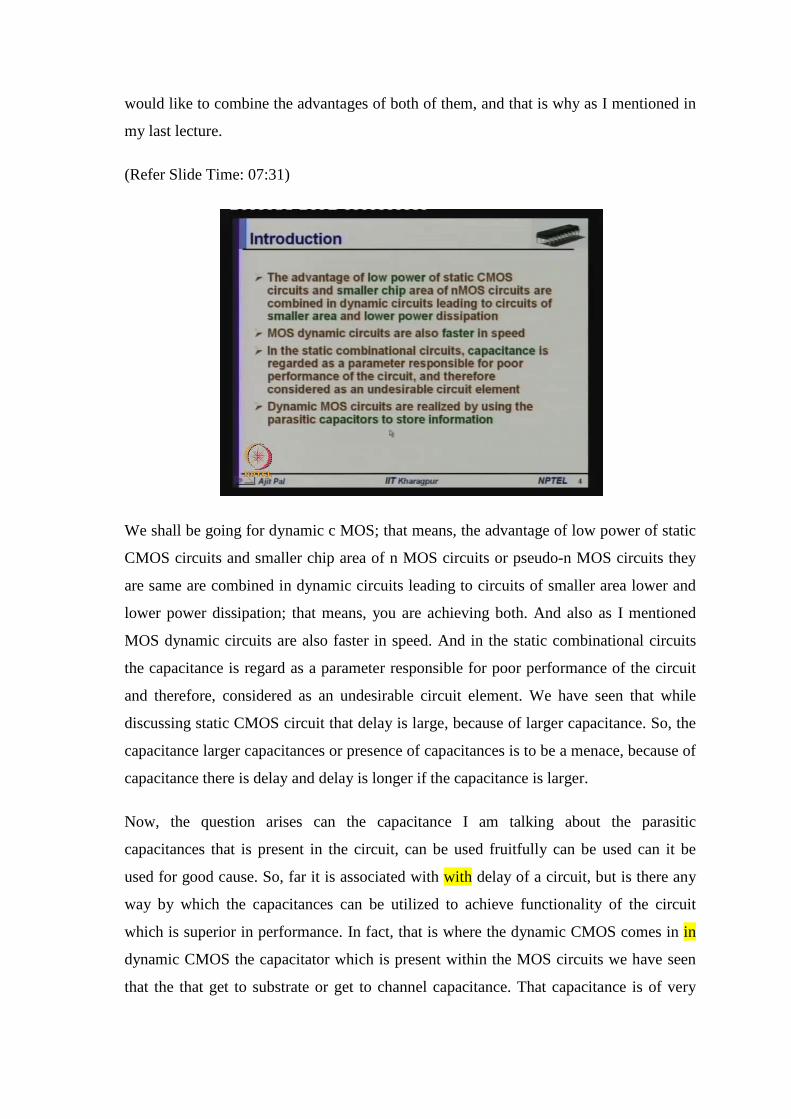
We shall be going for dynamic c MOS; that means, the advantage of low power of static
CMOS circuits and smaller chip area of n MOS circuits or pseudo-n MOS circuits they
are same are combined in dynamic circuits leading to circuits of smaller area lower and
lower power dissipation; that means, you are achieving both. And also as I mentioned
MOS dynamic circuits are also faster in speed. And in the static combinational circuits
the capacitance is regard as a parameter responsible for poor performance of the circuit
and therefore, considered as an undesirable circuit element. We have seen that while
discussing static CMOS circuit that delay is large, because of larger capacitance. So, the
capacitance larger capacitances or presence of capacitances is to be a menace, because of
capacitance there is delay and delay is longer if the capacitance is larger.
Now, the question arises can the capacitance I am talking about the parasitic
capacitances that is present in the circuit, can be used fruitfully can be used can it be
used for good cause. So, far it is associated with with delay of a circuit, but is there any
way by which the capacitances can be utilized to achieve functionality of the circuit
which is superior in performance. In fact, that is where the dynamic CMOS comes in in
dynamic CMOS the capacitator which is present within the MOS circuits we have seen
that the that get to substrate or get to channel capacitance. That capacitance is of very
good quality, because of good quality silicon dioxide layer that is created thin oxide layer
that is created and that capacitance we shall exploit or utilize how.
We know that a capacitor can be used to store charge. So, since a capacitor can be used
to store charge can we develop circuit for the capacitor intrinsic capacitor should be used
to store charge and that will be used for implementing circuit operation. And in fact, we
shall see that dynamic circuits exactly does that dynamic MOS circuits are realized by
using parasitic capacitors to store information. This is also done in a in a memory
elements as you know dynamic ram that is used in almost all systems, they are also these
the capacitors are utilized to store information, but here we are talking about realizing
combinational circuit, by storing information in those parasitic capacitors.
Question naturally arises are they free from any disadvantages; obviously, in this world
nothing is one sided we shall as we shall see, it will be dynamic CMOS circuits have
many advantages there will be many limitations as well. So, our objective will be to
design circuits which will overcome the limitations and utilize the good features.
(Refer Slide Time: 11:17)
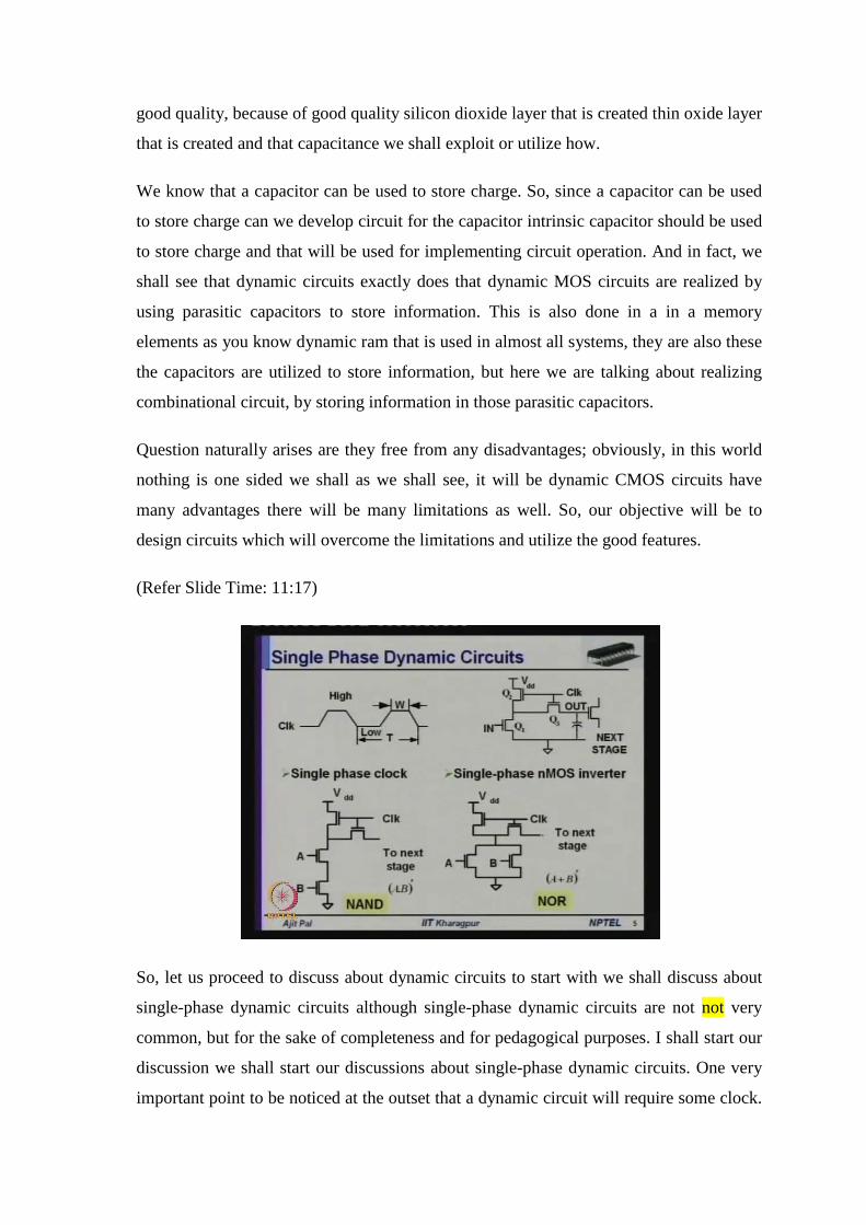
So, let us proceed to discuss about dynamic circuits to start with we shall discuss about
single-phase dynamic circuits although single-phase dynamic circuits are not not very
common, but for the sake of completeness and for pedagogical purposes. I shall start our
discussion we shall start our discussions about single-phase dynamic circuits. One very
important point to be noticed at the outset that a dynamic circuit will require some clock.
So, far we have seen that either nMOS or pseudo-nMOS or static CMOS circuits do not
require any clock for their operation. So, clock was not present particularly when we are
realizing combinational circuit, but as we shall see dynamic circuits will always require
some clock.
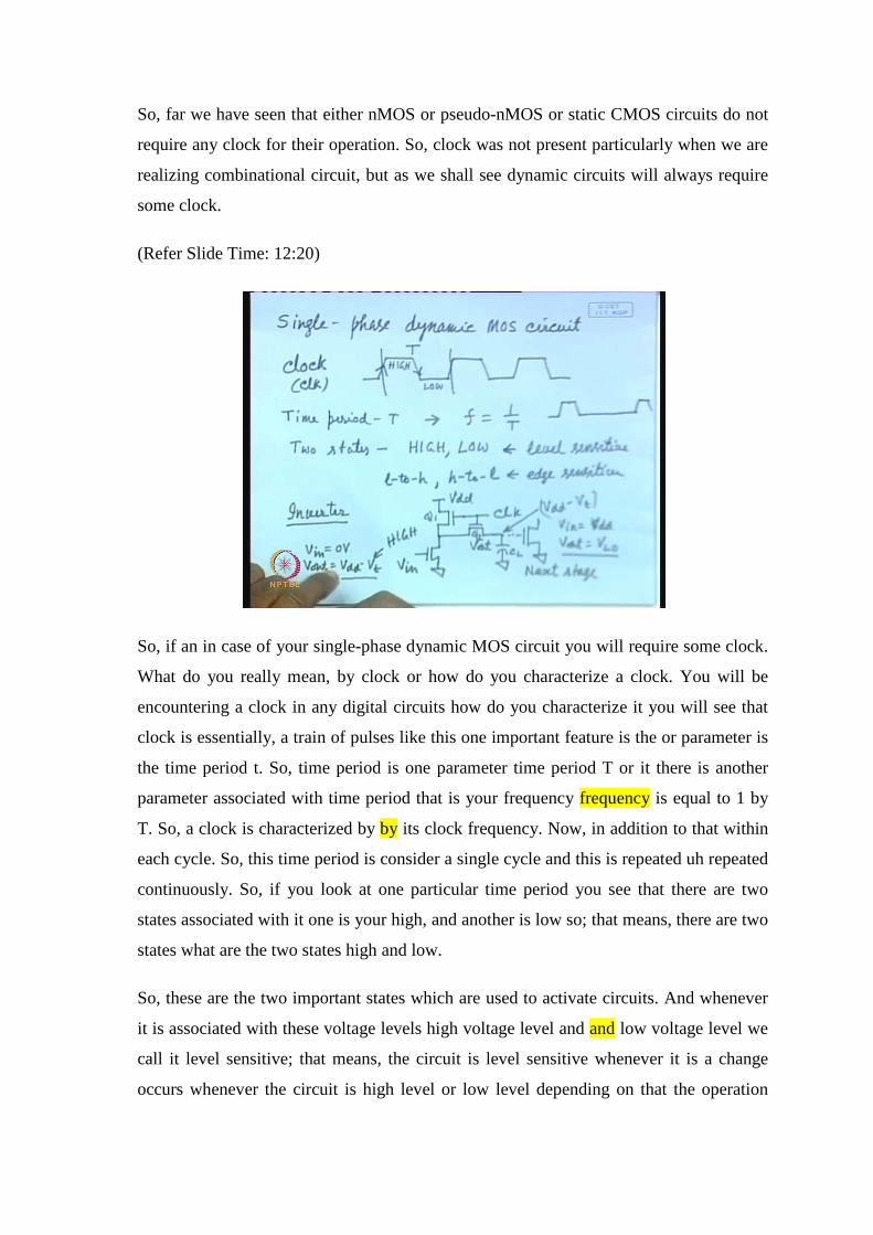
(Refer Slide Time: 12:20)
So, if an in case of your single-phase dynamic MOS circuit you will require some clock.
What do you really mean, by clock or how do you characterize a clock. You will be
encountering a clock in any digital circuits how do you characterize it you will see that
clock is essentially, a train of pulses like this one important feature is the or parameter is
the time period t. So, time period is one parameter time period T or it there is another
parameter associated with time period that is your frequency frequency is equal to 1 by
T. So, a clock is characterized by by its clock frequency. Now, in addition to that within
each cycle. So, this time period is consider a single cycle and this is repeated uh repeated
continuously. So, if you look at one particular time period you see that there are two
states associated with it one is your high, and another is low so; that means, there are two
states what are the two states high and low.
So, these are the two important states which are used to activate circuits. And whenever
it is associated with these voltage levels high voltage level and and low voltage level we
call it level sensitive; that means, the circuit is level sensitive whenever it is a change
occurs whenever the circuit is high level or low level depending on that the operation
changes. Another characteristic parameter is also there you know there is you can see
each period has got two transitions low to high and high to low. And these are called
edge sensitive. They are circuits which are sensitive to edge; that means, here low to high
and high to low. So, there are two edges in each period. So, the events can occur or can
be initiated either by changing level or by changing edges. So, for as the MOS dynamic
circuits are concern as we shall see these are level sensitive; that means, based on level
the operation of the circuit changes. Let us draw a very simple single-phase dynamic
MOS inverter. How do you realize an inverter, actually you realize you require two
transistors connected in this phone, and here you apply a clock say this clock in simple
form we usually write is c l clock clock is applied and here we apply Vdd then we have
the traditional pull down transistor present here, this is your pull down transistor and we
apply an input here, and we take the output not from here, but from this point.
So, here is the output point. So, V out and of course, it will have some associated
capacitance as you know, because it is feeding to a next stage and which may be a MOS
transistor. So, it is it is going to the next stage. How it works based on the single-phase
clock you have applied a clock here, and you have applied input here, and you are taking
the output from here. How it works when this clock is high these transistors q 1 and q 2
both are on. So, when the clock is high both the transistors run, and an as a consequence
what will happen what get at the output.
Whenever clock is high and input let us assume there are two conditions your V in is
equal to 0 volt. Whenever V in is equal to 0 this transistor is off, as a consequence what
will happen this capacitor this load capacitor c l will charge to Vdd through these two
transistors and you have applied a clock here. So, these two transistors will remain on.
Of course here you will get a voltage which is equal to Vdd minus V t not Vdd, because
you know the transistor will go off as the voltage goes above Vdd minus V t V t is the
threshold voltage of the n MOS transistor. So, you are getting a high level voltage which
is Vdd minus V t. Now what about the case now if you whenever the clock is going
down; that means, whenever it is in the low level then what happens, then what happens
the voltage which is the capacitor which is charged to Vdd minus V t that remains there.
That remains that is available here which we will feed to the next stage; that means, next
stage we utilize this logic level; that means, it is assumed that output is now Vdd minus
V t; that means, V out is equal to Vdd minus V t which is consider to be high because
input is low. Now, let us consider the situation when V in is equal to say 5 volt or Vdd
then what will happen whenever it is Vdd. Then you can see these transistors are on this
transistor is also non on what will be the voltage here, voltage will be dependent on the
ratio of the w y l of this transistor and w y l of this transistor. So, the behavior is identical
to that of you know static n MOS circuits. So, we get a V out which is equal to V low of
course, this is not zero which will be dependent on the ratio of the l by w ratio of these
transistor and that is why we can say that this is a this is a this is ratioed logic.
Now, what is the gain that we have achieved in this case, gain is that what you can do
you can make this period; that means, high level very small. I mean, this period can be
small this this I mean high level small and low level longer, by that what will what will
you achieve you will achieve that power dissipation will occur; that means, this power
dissipation can occur only when this clock is high. Earlier respective of the presence of
clock as long as output was low, there was power dissipation in static CMOS a static n
MOS circuits, but in this particular case only when the output is high. I mean, clock is
high and the output is low then there is static power dissipation. So, the static power
dissipation is reduced to a great extent, but there is static power dissipation and it is
ratioed logic, but the static power dissipation is much lower compared to your static
nMOS circuits or pseudo-nMOS circuits; however, you do not get good quality high
level and good quality low level both the levels are you know are weak not strong high
or strong low.
So, these circuits are not very popular, because of these limitations and although for this
say sake of completeness we are discussing it. And In fact, not only inverter you can
realized NAND gate as you can see only requirement is that you will require additional
transistors in the pMOS nMOS network pull down network. So, to input NAND gate we
will require two transistors to neither input nor gate we will require two transistors in this
way the number of transistors that is required is equal to n plus 2. So, n number of
transistors for the n inputs, and two transistors are required these two transistors q 1 and
q 2. So, these two additional transistors are required apart from n transistors where
primary inputs are applied. So, you see the number of transistors is reduced. So, these
circuits will be faster than static cMOS; however, we have discussed various limitations
of this.
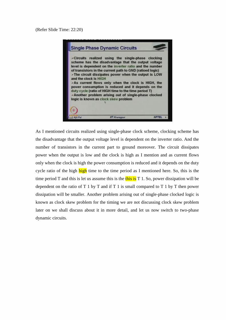
(Refer Slide Time: 22:20)
As I mentioned circuits realized using single-phase clock scheme, clocking scheme has
the disadvantage that the output voltage level is dependent on the inverter ratio. And the
number of transistors in the current part to ground moreover. The circuit dissipates
power when the output is low and the clock is high as I mention and as current flows
only when the clock is high the power consumption is reduced and it depends on the duty
cycle ratio of the high high time to the time period as I mentioned here. So, this is the
time period T and this is let us assume this is the this is T 1. So, power dissipation will be
dependent on the ratio of T 1 by T and if T 1 is small compared to T 1 by T then power
dissipation will be smaller. Another problem arising out of single-phase clocked logic is
known as clock skew problem for the timing we are not discussing clock skew problem
later on we shall discuss about it in more detail, and let us now switch to two-phase
dynamic circuits.
(Refer Slide Time: 23:26)
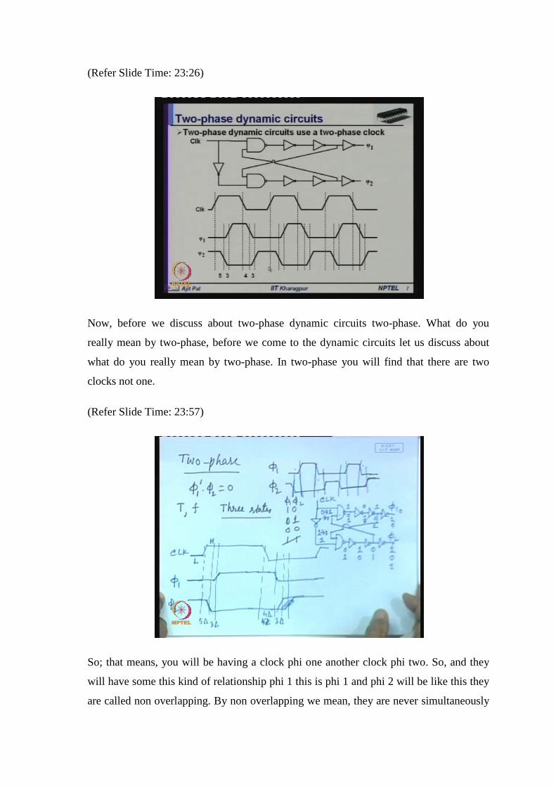
Now, before we discuss about two-phase dynamic circuits two-phase. What do you
really mean by two-phase, before we come to the dynamic circuits let us discuss about
what do you really mean by two-phase. In two-phase you will find that there are two
clocks not one.
(Refer Slide Time: 23:57)
So; that means, you will be having a clock phi one another clock phi two. So, and they
will have some this kind of relationship phi 1 this is phi 1 and phi 2 will be like this they
are called non overlapping. By non overlapping we mean, they are never simultaneously
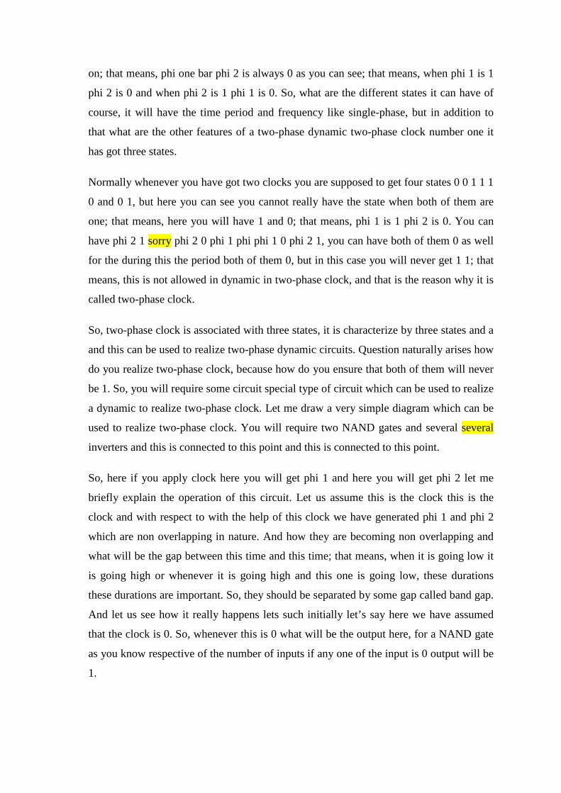
on; that means, phi one bar phi 2 is always 0 as you can see; that means, when phi 1 is 1
phi 2 is 0 and when phi 2 is 1 phi 1 is 0. So, what are the different states it can have of
course, it will have the time period and frequency like single-phase, but in addition to
that what are the other features of a two-phase dynamic two-phase clock number one it
has got three states.
Normally whenever you have got two clocks you are supposed to get four states 0 0 1 1 1
0 and 0 1, but here you can see you cannot really have the state when both of them are
one; that means, here you will have 1 and 0; that means, phi 1 is 1 phi 2 is 0. You can
have phi 2 1 sorry phi 2 0 phi 1 phi phi 1 0 phi 2 1, you can have both of them 0 as well
for the during this the period both of them 0, but in this case you will never get 1 1; that
means, this is not allowed in dynamic in two-phase clock, and that is the reason why it is
called two-phase clock.
So, two-phase clock is associated with three states, it is characterize by three states and a
and this can be used to realize two-phase dynamic circuits. Question naturally arises how
do you realize two-phase clock, because how do you ensure that both of them will never
be 1. So, you will require some circuit special type of circuit which can be used to realize
a dynamic to realize two-phase clock. Let me draw a very simple diagram which can be
used to realize two-phase clock. You will require two NAND gates and several several
inverters and this is connected to this point and this is connected to this point.
So, here if you apply clock here you will get phi 1 and here you will get phi 2 let me
briefly explain the operation of this circuit. Let us assume this is the clock this is the
clock and with respect to with the help of this clock we have generated phi 1 and phi 2
which are non overlapping in nature. And how they are becoming non overlapping and
what will be the gap between this time and this time; that means, when it is going low it
is going high or whenever it is going high and this one is going low, these durations
these durations are important. So, they should be separated by some gap called band gap.
And let us see how it really happens lets such initially let’s say here we have assumed
that the clock is 0. So, whenever this is 0 what will be the output here, for a NAND gate
as you know respective of the number of inputs if any one of the input is 0 output will be
1.
So, since this is 0 this will be 1 this will be 0 this will be 1 and this will be zero; that
means, we are getting that it phi one is also 0 when clock is 0 phi one is also 0. What
about phi 2 here this since this is 0 this is 1, and here also it is 1. So, 1 makes it 0 this is
one this is 0 and this is 1. So, as expected the phi 2 is high. So, here it is low and here it
is high. Now, at this point it has switched from low to high. So, as it switches from low
to high that is 1. What happens whenever it switches to 0 to 1 this will switch to 1 to 0
after 1 gate delay, and as you know for a non gate a NAND gate whenever any one of the
input is 0 output will immediately change. So, this will change to 0 to 1 this will change
to 1 to 0, this will change to 0 to 1, this will change to 1 to 0 after how much time say
how many got gate delays 1, 2, 3, 4, 5 after 5 gate delays phi 2 is become phi 2 is going
phi 2 is becoming low.
So, let us assume this is the 5 gate delay after 5 gate delay this will go low. Then as you
can see here, this is now 1 and this is also 1 these two will make it 0 this will make it one
this will make it 0 and this will make it 1. So, this will switch to 1, but how after how
much time after this has become say this has become 1 and this is already 1. So, when
both of them becomes one after that one two three four; that means, here it will be 1, 2,
3, 4, 5, 6, 7, 8 after 8 gate delays this will switch from 1 to 0 earlier it was one now it
will become it has become 0. So, it will become 8 gate delays. So, this is 5 delta and here
will be another 3 delta when it will go from low to high.
And this will continue until another change occurs here. So, whenever again it switches
from 1 to 0 I mean, 1 to 0 it is switching now to 0. And as it switches to 0 this will now
change from 0 to 1 since this is 0 it will become 1 again this will become 0 this will
become 1 this will become 0, but after how much time. So, we can see as it is changing
from this input is changing from 1 to 0 here 1, 2, 3, 4 after 4 gate delays it will become 0;
that means, phi 1 will become 0 from this edge after 4 gate delays. And as it has happen
this becomes 1 this is also 1, again after three gate delays up from that it will become
switch it will switch to 1; that means, this will switch to 1 after 3 gate delays from this 3
gate delays and this will continue.
So, we can see here we have got 5 gate delay here 3 gate delay here 4 gate delay here and
this to this it is sorry not this 1, this to this 4 gate delay and from this edge to actually it
should be here 3 delta. So, we find that in this particular case here, there is a gap of 3
gate delay here also there is gap of 3 gate delay here. Similarly, for the other case also
there will be 3 gate delay; that means, this part this one the gap between these two edges
will be 3 delta gap between these two edges will be 3 delta gap between these two edges
will be three delta gap between these two edges will be 3 delta.
So, this is how you can realize a two-phase clock with the help of few inverters two
NAND gates from a single-phase clock. You may say say you may ask that suppose we
are not satisfied with a 3 delta band gap between the two-phase clocks. Then what you
can do you can insert more number of inverters here, say instead of 3 you can have 5
here then this will become this gap will be 5 delta 5 delta 5 delta and so on. So,
depending on your requirement you can increase the gap between the two-phase clocks,
but that non overlapping property will be always maintained whenever you will generate
two-phase clock by using this technique. So, much about two-phase clock. So, here we
have shown the same thing and how continuously you will get two-phase clock phi 1 and
phi 2 maintaining 3 gate delays at both edges here also 3 get delay three get delay and so
on.
(Refer Slide Time: 34:27)
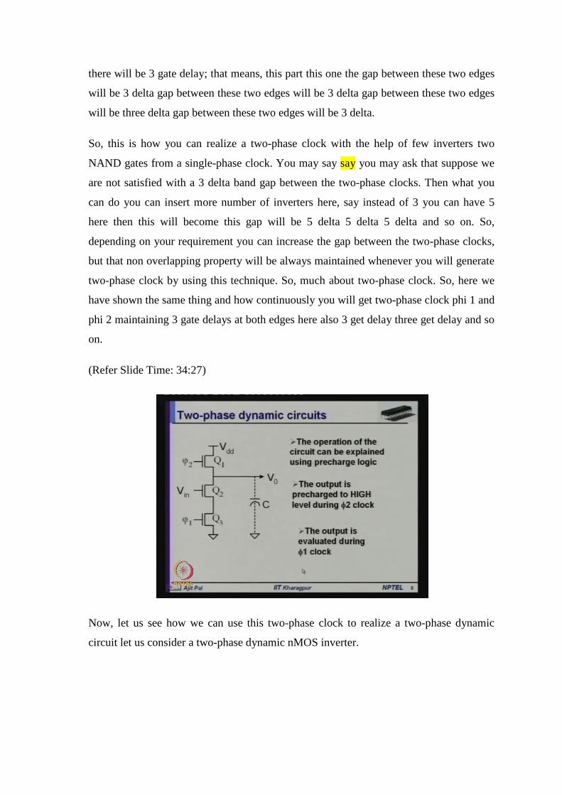
Now, let us see how we can use this two-phase clock to realize a two-phase dynamic
circuit let us consider a two-phase dynamic nMOS inverter.
(Refer Slide Time: 34:38)
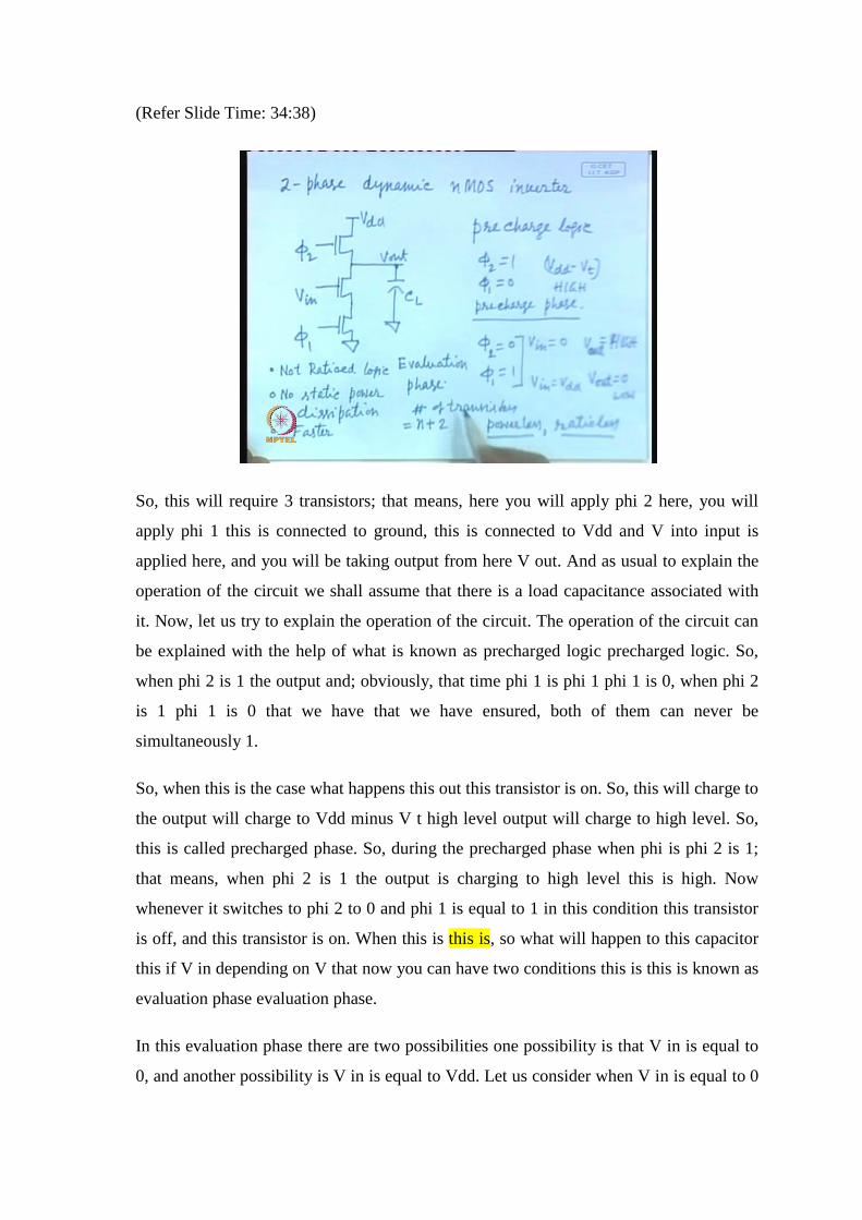
So, this will require 3 transistors; that means, here you will apply phi 2 here, you will
apply phi 1 this is connected to ground, this is connected to Vdd and V into input is
applied here, and you will be taking output from here V out. And as usual to explain the
operation of the circuit we shall assume that there is a load capacitance associated with
it. Now, let us try to explain the operation of the circuit. The operation of the circuit can
be explained with the help of what is known as precharged logic precharged logic. So,
when phi 2 is 1 the output and; obviously, that time phi 1 is phi 1 phi 1 is 0, when phi 2
is 1 phi 1 is 0 that we have that we have ensured, both of them can never be
simultaneously 1.
So, when this is the case what happens this out this transistor is on. So, this will charge to
the output will charge to Vdd minus V t high level output will charge to high level. So,
this is called precharged phase. So, during the precharged phase when phi is phi 2 is 1;
that means, when phi 2 is 1 the output is charging to high level this is high. Now
whenever it switches to phi 2 to 0 and phi 1 is equal to 1 in this condition this transistor
is off, and this transistor is on. When this is this is, so what will happen to this capacitor
this if V in depending on V that now you can have two conditions this is this is known as
evaluation phase evaluation phase.
In this evaluation phase there are two possibilities one possibility is that V in is equal to
0, and another possibility is V in is equal to Vdd. Let us consider when V in is equal to 0
when V in is equal to 0 this transistor is off and although phi 2 is 1 this transistor is on
there is no path to dispatch this capacitor so; that means, V out is equal to Vdd I mean is
high V out is equal to high why it is high, because which the capacitor has is already
charged to high level during the precharged phase. And the evaluation phase follows the
precharged phase and as a consequence the high level is maintained during evaluation
phase and which will be used by the next stage. So, after evaluation after the evaluation
is done a valued output is available which will be used by the next stage.
Now, let us assume V in is equal to Vdd. When V in is equal to Vdd both the transistors
are on and capacitor will discharge to 0 logic level so; that means, in that case V out will
be equal to 0 or low logic level. So, here of course, you will get strong low logic level.
So, what is the advantage of this circuit we are able to get two possible outputs and of
course, high logic level is not very good, but low logic level is good, because it is not
ratioed logic. Number one this two-phase dynamic circuit is not ratioed logic. There is no
static power dissipation. So, let us list the advantages and disadvantages.
So, maybe we can discuss about the advantages and disadvantages very quickly before
we come to other circuits advantages it is not ratioed logic. So, disadvantages associated
with ratioed logic is overcome no static power dissipation. Third is faster much faster
than either pseudo-n MOS or static CMOS and number of transistors as we have seen is
equal to n plus two number of transistors is equal to n plus 2.
So, these are the advantages of this two-phase dynamics n MOS circuit. So, we find that
it has got very good features and that is the reason why it is called powerless ratio less
powerless, because there is no static power dissipation and ratio less, because it is not
rationed logic and of course, it is faster in operation. So, these two-phase dynamic n
MOS inverter is has got very good features and it is widely used; however, you are more
interested in u h CMOS circuits.
(Refer Slide Time: 41:05)
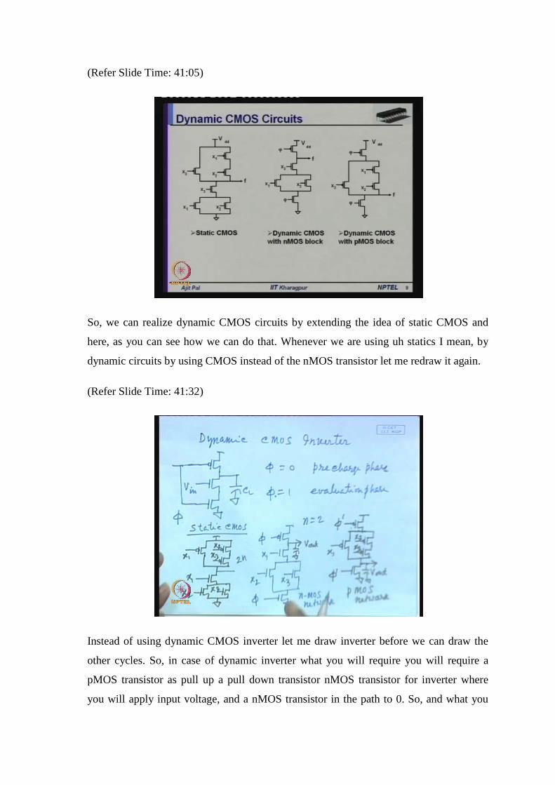
So, we can realize dynamic CMOS circuits by extending the idea of static CMOS and
here, as you can see how we can do that. Whenever we are using uh statics I mean, by
dynamic circuits by using CMOS instead of the nMOS transistor let me redraw it again.
(Refer Slide Time: 41:32)
Instead of using dynamic CMOS inverter let me draw inverter before we can draw the
other cycles. So, in case of dynamic inverter what you will require you will require a
pMOS transistor as pull up a pull down transistor nMOS transistor for inverter where
you will apply input voltage, and a nMOS transistor in the path to 0. So, and what you
can do you can apply a clock you do not really require two-phase clock whenever you
are realizing dynamic CMOS circuit the reason for that is you can see the same if we
apply the same signal to the pMOS and nMOS transistor, when p this phi is 0 this
transistor is on and when phi is 1 this transistor is on.
So, that the requirement for that that phi 1 and phi 2 should not be simultaneously on is
satisfied very easily. So, we do not really require two-phase clock in realizing dynamic
CMOS circuit. The operation is identical to the inverter that we have discussed two-
phase dynamic n MOS inverter here, what happens when when phi 2 when phi is equal
to 0, it is in the precharge phase this output charges to high logic level. And when phi phi
is equal to 1 then it is called evaluation phase.
The output is evaluated depending on the input this V in. So, this is how you can realize
a dynamic CMOS inverter and all the advantages that I mention in the context of this
two-phase dynamic n MOS inverter are applicable to dynamic CMOS inverter. It is not
ratioed logic there is no static power dissipation it is faster number of transistor required
is equal to n plus 2 and it is also powerless and ratio less. So, all the advantages are
carried to this dynamic CMOS inverter.
You can realize dynamic CMOS inverter I mean, extend this concept to realize more
complex gates. Let us consider a first of all static CMOS and we shall see real we shall
consider the realization dynamic CMOS circuits corresponding to that. Let us assume
that it is little complex circuit. So, you have got say x 1, x 2, x 3 and then you have got x
1, x 2, x 3 connected to down. So, this is your static CMOS circuits we want a dynamic
CMOS circuit which is which performs the same function. What we can do you will you
may use you can see as I mentioned earlier you are repeating two logic circuits to realize
the function we shall see we can use only one of them to realize a dynamic CMOS circuit
Let us see how we can realize this function by using only the n MOS network circuit. So,
what will you do you can realize the dynamic CMOS circuits x 1, x 2, x 3 and here you
will put one nMOS transistor and here you will put one p MOS transistor and you will
apply clock here. So, you can see you do not have really duplicate the logic function here
you will require only the nMOS network part which is present here to realize the
dynamic CMOS circuit. Of course, you will require two additional transistor that is here
you will require n plus two transistors instead of two n as you require in static CMOS.
Now is it the only way to realize dynamic CMOS circuit, actually you can use either the
n MOS network or the p MOS network here. The circuit that has been realized is using
the n MOS network.
What you can do you can use the same you can realize the same circuit by using the p
MOS network. So, in that case the topology will be like this same network x 1, then x 2,
x 3, but you will require again two transistors one at the bottom and another the top. So,
you will apply phi bar you will apply phi or you can apply phi bar actually. Now, where
from you will take the output here you were taking the output from here. So, this was
your V out, but whenever used pMOS network in that case you have to take the output
from the this point bottom; that means, V out is from here how this circuit operates here
actually again it is based on precharge approach, but instead of precharging the output to
high level as you do it here you are actually predischarging the output to low level in this
particular case; that means, whenever you are using the pMOS network then the output is
predischarged during the precharged phase; that means, this transistor is on you have
applied phi bar. So, this transistor will be on when this is high.
Or phi is equal to 0. So, when this is high this transistor will be discharged during
precharged phase that is being done. So, this is discharged to 0 and during evaluation
what will happen depending on the input combinations input vector; that means,
depending on the values of x 1, x 2 and x 3, you can uh this output will be charged to
high level if the input combination is such the output should be high in that case if
there’ll be a path through this through this network during the evaluation phase when this
transistor is on and the there will be path through this pMOS network. So, this will in the
during evaluation phase it will charged to Vdd level.
But if the if the output is 0 then it will remain in that pre-discharged condition, it will not
charged to V v d level. So, you can see we have two possible alternatives whenever we
realize circuits using dynamic CMOS approach either you can use the n MOS network or
you can use the p MOS network, but you do not have to duplicate; that means, use this as
well as that as you do in case of static CMOS and you may have been asking which one
will be faster and of course, the network I mean the topology using nMOS network could
be faster with the same area, because as you know the pMOS transistors will take uh will
take longer time, because of higher resistance and lower mobility of the holes compared
to electrons an as a consequence for the same area the this particular topology will be
requiring larger time it will be slower than this one. However both are used later on we
shall see both can be combined in realizing a special type of circuit there later on we
shall discuss about it for the time being let us restrict to this now very quickly.
(Refer Slide Time: 50:41)
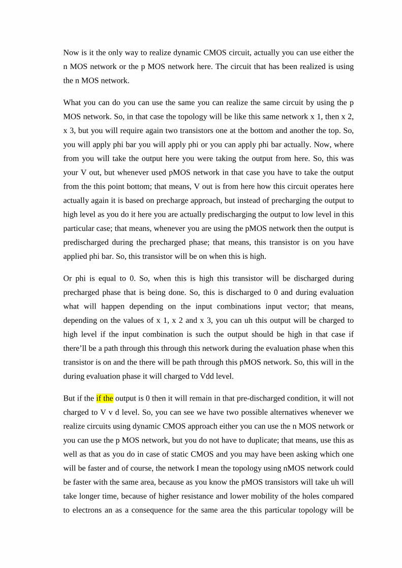
Let us have a look at the disadvantages advantages and disadvantages. As I have already
mentioned, the number of transistors required for a circuit with fan-in N is N plus 2 in
contrast to 2N in case of static CMOS circuits. The load capacitance is more than 50
percent less than static CMOS and is closer to that of nMOS circuits as a consequence it
is faster. So, the speed of operation is faster than that of static CMOS circuits about 4 to
5 times faster as we have we have found that; and there is no static power dissipation and
another important point is there is no short circuit power dissipation, why there is no
short circuit power dissipation, because at no point of time there is path from Vdd to
ground even when the input changes, because it is controlled by clock and as a
consequence it is since it is controlled by clock, there will be no path from V d to would
to V d to ground at any point of time, and as consequence there is no short circuit power
dissipation.
And later on we shall see that it has got no glitching power dissipation why it has got no
glitching power dissipation. As you know glitching power dissipation occurs because of
you know changes at the output within the circuit, because of the delay of the circuit, but
here it is more or less synchronized by clock and only one transition is possible you
know after it has been precharged only transition that can occur is from high to low no
other transition is possible, but in case of static CMOS circuits the particular node can go
through number of charging and discharging before attempting the final value and as a
consequence the glitching power dissipation is not present in dynamic CMOS circuits.
And as a consequence the dynamic CMOS circuits have been found to be very suitable,
because of theirs higher speed of operation and lower area. In fact, one of the very
important processor dekalpha chip you may have heard of it that dekalpha processor was
one of the fastest processor I mean introduced long back and there they have used about
30 percent of their circuits using dynamic CMOS. Essentially the critical parts of the
circuits were implemented by using dynamic CMOS circuit. So, that they can achieve
very high speed of operation any way those are the advantages and based on those
advantages this is done, but there are several disadvantages.
(Refer Slide Time: 53:17)
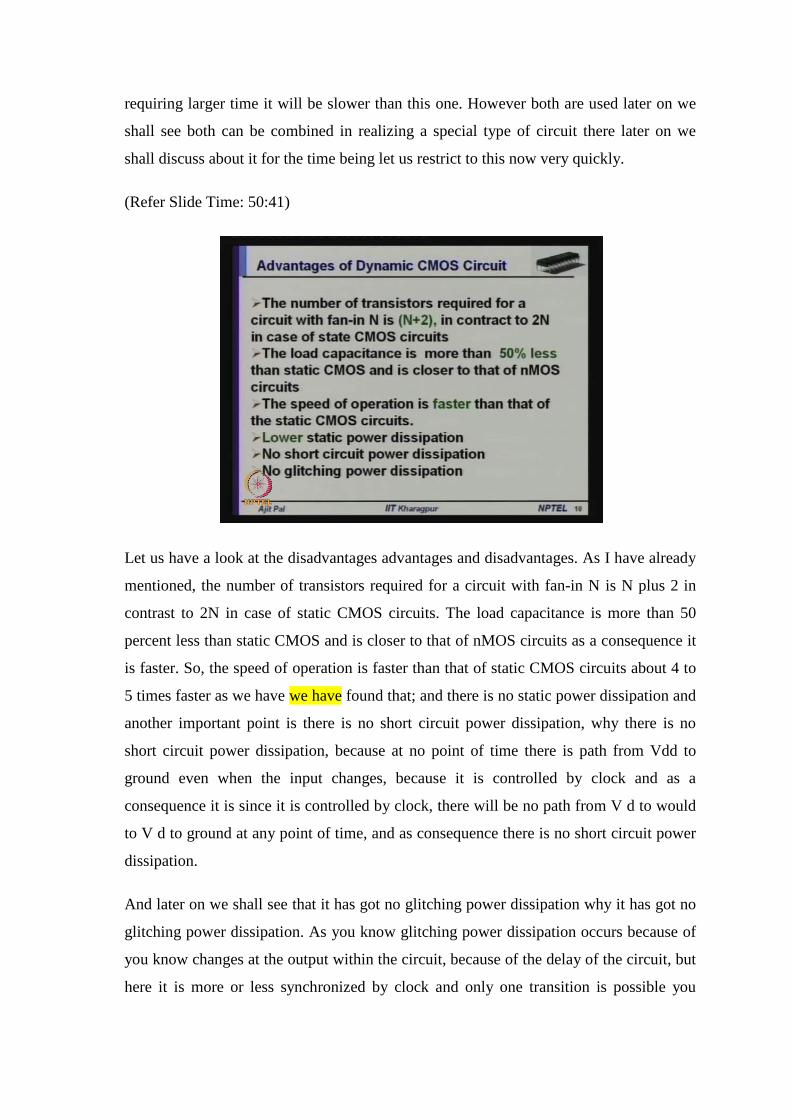
Number one is charge leakage problem, number two is charge sharing problem and third
is clock skew problem. So, these are the three problems associated with dynamic CMOS
circuits. And in my next lecture, I shall discuss about these disadvantages, and also we
shall discuss about how they can be overcome. Obviously, if we accept the
disadvantages, then we cannot realize a circuit, we have to develop technique by which
these limitations and disadvantages can be overcome, and which we shall discuss in my
next lecture thank you.