Low-Power Touch Through Glass Reference Design · Low-Power Touch Through Glass Reference Design 3...
23
TIDA-00343 Copyright © 2016, Texas Instruments Incorporated USB I 2 C GPIO +3.3 V CapTIvate FR2633 &DS7,YDWH PGMR T T 1 TIDUBJ7 – April 2016 Submit Documentation Feedback Copyright © 2016, Texas Instruments Incorporated Low-Power Touch Through Glass Reference Design TI Designs Low-Power Touch Through Glass Reference Design Design Overview The human machine interface (HMI) is an essential part of process plants because it is one of the major ways through which humans and machines interact. The TIDA-00343 reference design offers an HMI solution for harsh and hazardous area applications. In process plants, operators are required to interact with explosion-proof displays or controllers, which are housed in screw-on metallic enclosures with thick glass windows to display local readout and programming functions. The TIDA-00343 TI Design, which uses CapTIvate™ innovative technology from TI, allows the operator to interact with a controller without requiring them to open the enclosure, which saves time by avoiding a work permit or plant shutdown. Design Resources TIDA-00343 Design Folder MSP430FR2633 Product Folder CapTIvate™ Tool Folder ASK Our E2E Experts Design Features • Single and Multistep Button Press • Four Robust Buttons Option Implemented • Four LEDs as Feedback • Variable Air Gap Between Buttons and Glass (1 mm to 2 mm) • Touch Detection Through Thick Glass (8 mm to 12 mm) • Work With Gloves and in Harsh Environment (Water, Oil, Dust, and So Forth) • Temperature Range: –40°C to 85°C Featured Applications • HMI • Process Control • Field Transmitters • Field Actuators An IMPORTANT NOTICE at the end of this TI reference design addresses authorized use, intellectual property matters and other important disclaimers and information.
Transcript of Low-Power Touch Through Glass Reference Design · Low-Power Touch Through Glass Reference Design 3...

TIDA-00343
Copyright © 2016, Texas Instruments Incorporated
USB
I2C
GPIO
+3.3 VCapTIvate�FR2633
&DS7,YDWH�
PGMR
T T
1TIDUBJ7–April 2016Submit Documentation Feedback
Copyright © 2016, Texas Instruments Incorporated
Low-Power Touch Through Glass Reference Design
TI DesignsLow-Power Touch Through Glass Reference Design
Design OverviewThe human machine interface (HMI) is an essentialpart of process plants because it is one of the majorways through which humans and machines interact.The TIDA-00343 reference design offers an HMIsolution for harsh and hazardous area applications. Inprocess plants, operators are required to interact withexplosion-proof displays or controllers, which arehoused in screw-on metallic enclosures with thickglass windows to display local readout andprogramming functions.The TIDA-00343 TI Design, which uses CapTIvate™innovative technology from TI, allows the operator tointeract with a controller without requiring them to openthe enclosure, which saves time by avoiding a workpermit or plant shutdown.
Design Resources
TIDA-00343 Design FolderMSP430FR2633 Product FolderCapTIvate™ Tool Folder
ASK Our E2E Experts
Design Features• Single and Multistep Button Press• Four Robust Buttons Option Implemented• Four LEDs as Feedback• Variable Air Gap Between Buttons and Glass
(1 mm to 2 mm)• Touch Detection Through Thick Glass
(8 mm to 12 mm)• Work With Gloves and in Harsh Environment
(Water, Oil, Dust, and So Forth)• Temperature Range: –40°C to 85°C
Featured Applications• HMI• Process Control• Field Transmitters• Field Actuators
An IMPORTANT NOTICE at the end of this TI reference design addresses authorized use, intellectual property matters and otherimportant disclaimers and information.

Key System Specifications www.ti.com
2 TIDUBJ7–April 2016Submit Documentation Feedback
Copyright © 2016, Texas Instruments Incorporated
Low-Power Touch Through Glass Reference Design
1 Key System Specifications
Table 1. Key System Specifications
PARAMETER SPECIFICATION DETAILSGlass thickness 9.5 mm See Section 3.2Glass diameter 80 mm See Section 3.2
Air gap 1 mm to 2 mm See Section 3.3Number of buttons Four See Section 3.3
Feedback LED —Work with gloves — See Section 8.2
Harsh environment resistant — See Section 8SNR — See Section 8
Crosstalk — See Section 8Low power (≈10-Hz scan rate) 240 µA (average) —
Temperature range –40°C to 85°C —
2 System DescriptionThe TIDA-00343 design combines a button board with a TI CapTIvate™ integrated circuit (IC). The buttonboard represents an operator interface and the CapTIvate IC processes the inputs given by an operator.
The complete system offers an HMI solution for harsh or difficult hazardous area applications in processplants that require operators to interact with an explosion-proof display or controller. Displays andcontrollers are housed in screw-on metallic enclosures with thick glass windows to display local readoutand programming functions.
The CapTIvate technology in this TI Design allows the operator to interact with the controller withoutrequiring them to open the enclosure, which saves time by avoiding a work permit or plant shutdown.
The CapTIvate technology provides high-resolution capacitive-touch sensing, which allows plant operatorsto touch buttons through the thick glass window while offering high reliability and noise immunity at thelowest power (see Figure 1).
Figure 1. Touch Through-Glass Application
7 5/8"5 3/4"
4"
3 5/16"
4 1/16"
5/16" Diameter Mounting Holes
5" 5 5/8"
1 3/32"
3/4" - 14 NPT(2) PLACES
5 7/16"
www.ti.com System Design Theory
3TIDUBJ7–April 2016Submit Documentation Feedback
Copyright © 2016, Texas Instruments Incorporated
Low-Power Touch Through Glass Reference Design
3 System Design TheoryThis section focuses on the design theory of the electrode board. For more information on CapTIvatetechnology, consult the following CapTIvate™ Technology Guide.
3.1 Mechanical DesignDesigning the electrode board requires attention to a few key mechanical details. Note that the board is tobe housed in a screw-on metallic enclosure (see Section 3.2), which can be removed by unscrewing theunit. To prevent any interference with the electronics when the user removes the enclosure, the electrodeboard must not be in direct contact with the glass window. The distance between the window glass andthe electrode board can vary depending on the application.
The typical placement of the electrode board is in the lower part of the glass window to leave space for aliquid-crystal display (LCD) on the upper part of the glass window for a local readout of the sensorparameters.
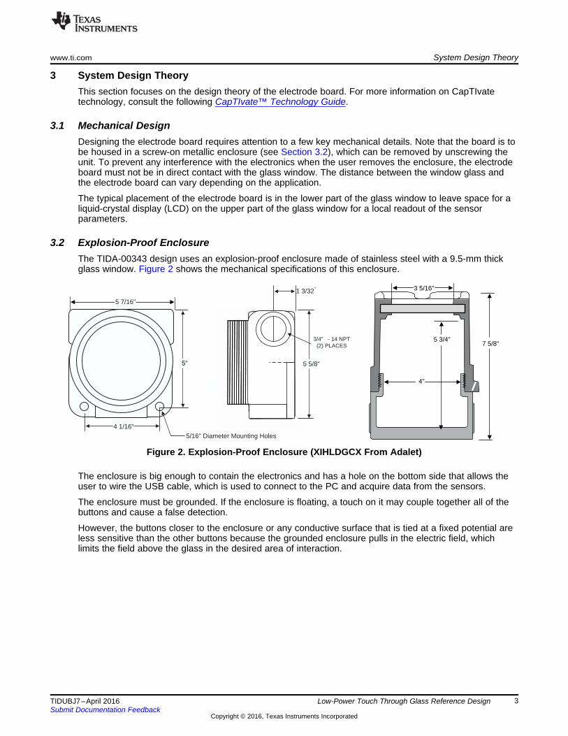
3.2 Explosion-Proof EnclosureThe TIDA-00343 design uses an explosion-proof enclosure made of stainless steel with a 9.5-mm thickglass window. Figure 2 shows the mechanical specifications of this enclosure.
Figure 2. Explosion-Proof Enclosure (XIHLDGCX From Adalet)
The enclosure is big enough to contain the electronics and has a hole on the bottom side that allows theuser to wire the USB cable, which is used to connect to the PC and acquire data from the sensors.
The enclosure must be grounded. If the enclosure is floating, a touch on it may couple together all of thebuttons and cause a false detection.
However, the buttons closer to the enclosure or any conductive surface that is tied at a fixed potential areless sensitive than the other buttons because the grounded enclosure pulls in the electric field, whichlimits the field above the glass in the desired area of interaction.

Glass
Air gap
Button
FR-4 CoreLaminate
Copper
A
Conductive plates
Dielectric
d
0rCA
d= ´ ´ò ò
System Design Theory www.ti.com
4 TIDUBJ7–April 2016Submit Documentation Feedback
Copyright © 2016, Texas Instruments Incorporated
Low-Power Touch Through Glass Reference Design
3.3 Electrode DesignThe diameter and shape of the electrodes are defined by a tradeoff between obtaining the maximumsensitivity (Equation 1) and the mechanical constraints of the application (see Figure 3).
(1)
Figure 3. Parallel Plate Capacitor
The area of the button must be as big as possible or at least the same size of the average finger press fora higher sensitivity. The button diameter of the TIDA-00343 is equal to 10 mm, which is a bit smaller thanthe average finger press of an operator and is limited by the mechanical constraints of the application.
This application typically requires the use of a glass window with a diameter that spans from 4 cm up to12 cm and contains three to six buttons, which are placed behind the glass on the lower section. In thissetup, the space for each button is approximately 1 cm to 2 cm without accounting for the minimumdistance required between the buttons, which is fundamental to avoiding crosstalk, and the spaceoccupied by the microcontroller (MCU), light-emitting diode (LED), and passives in the printed circuit board(PCB).
A medium-sized enclosure has an 8-cm glass window diameter and a four-button application. To accountfor the application requirements of this design, the TIDA-00343 has four buttons with 10-mm diameters.
Section 3.1 explains the importance of placing the buttons a certain distance from the metallic enclosure.Additionally, the buttons must be placed as far as possible from each other to avoid crosstalk, whichincreases as the air gap between the glass and buttons increase. Note that the dielectric of this applicationis not negligible (see Figure 4).
Figure 4. Application Stackup
10mmthick glass
38
80
24
31
23.3
13.2
11.4
8.9
15.8
All the measurements are in mm
GroundedMetalenclosure
www.ti.com System Design Theory
5TIDUBJ7–April 2016Submit Documentation Feedback
Copyright © 2016, Texas Instruments Incorporated
Low-Power Touch Through Glass Reference Design
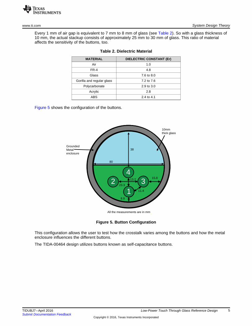
Every 1 mm of air gap is equivalent to 7 mm to 8 mm of glass (see Table 2). So with a glass thickness of10 mm, the actual stackup consists of approximately 25 mm to 30 mm of glass. This ratio of materialaffects the sensitivity of the buttons, too.
Table 2. Dielectric Material
MATERIAL DIELECTRIC CONSTANT (Er)Air 1.0
FR-4 4.8Glass 7.6 to 8.0
Gorilla and regular glass 7.2 to 7.6Polycarbonate 2.9 to 3.0
Acrylic 2.8ABS 2.4 to 4.1
Figure 5 shows the configuration of the buttons.
Figure 5. Button Configuration
This configuration allows the user to test how the crosstalk varies among the buttons and how the metalenclosure influences the different buttons.
The TIDA-00464 design utilizes buttons known as self-capacitance buttons.

PCBTX/RX
Front panel
System Design Theory www.ti.com
6 TIDUBJ7–April 2016Submit Documentation Feedback
Copyright © 2016, Texas Instruments Incorporated
Low-Power Touch Through Glass Reference Design
3.4 Self-Capacitive ButtonsA self-capacitive button sensor is a single electrode. Self-capacitive buttons are simple to lay out and eachbutton is assigned to only one pin on the MCU (see Figure 6). Self-capacitive buttons provide greatersensitivity as compared to a mutual capacitive button, but are more influenced by parasitic capacitances toground.
Figure 6. Example Diagram—Self-Capacitive Button Design
Table 3 shows the basic specifications of self-capacitive buttons.
Table 3. Self-Capacitive Button Properties
PARAMETER GUIDANCERadiation pattern Between electrode and ground
Size Equivalent to interactionShape Various: typically round or square
Spacing 0.5 × overlay minimum thickness
3.4.1 Self-Capacitive Button ShapesThe electrode shape is typically rectangular or round with common sizes of 10 mm and 12 mm. Ultimately,the size depends on the required touch area. A good design practice is to keep the size of the button assmall as possible, which minimizes the capacitance and helps with the following:• Reduce susceptibility to noise• Improve sensitivity• Lower power operation as a result of smaller capacitance and reduced electrode scan time
Figure 7 shows an example of a silkscreen-button outline pattern.
Figure 7. Silkscreen-Button Outline Pattern
DecalElectrode
Effective area for
larger finger
Larger Finger Size
DecalElectrode
Smaller Finger Size
Effective area for
smaller finger
10 mm
5 mm
Overlay
Electrode
Decal
PCB
Ground Pour
15 mm
Finger Sizes
6 mm
DecalElectrode
Effective area for
larger finger
Larger Finger Size
DecalElectrode
Smaller Finger Size
Effective area for
smaller finger
10 mm
5 mm
Overlay
Electrode
Decal
PCB
Ground Pour
20 mm 14 mm
Finger Sizes
www.ti.com System Design Theory
7TIDUBJ7–April 2016Submit Documentation Feedback
Copyright © 2016, Texas Instruments Incorporated
Low-Power Touch Through Glass Reference Design
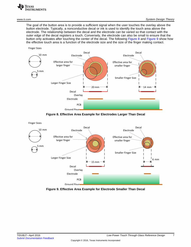
The goal of the button area is to provide a sufficient signal when the user touches the overlay above thebutton electrode. Typically, a nonconductive decal or ink is used to identify the touch area above theelectrode. The relationship between the decal and the electrode can be varied so that contact with theouter edge of the decal registers a touch. Conversely, the electrode can also be small to ensure that thebutton only activates after touching the center of the decal. The following Figure 8 and Figure 9 show howthe effective touch area is a function of the electrode size and the size of the finger making contact.
Figure 8. Effective Area Example for Electrodes Larger Than Decal
Figure 9. Effective Area Example for Electrode Smaller Than Decal

Overlay
Do not shape electrodesto identify function
Do use solid shapes andnonconductive decals or
ink to identify function
Electrode ElectrodeElectrode
Decals
System Design Theory www.ti.com
8 TIDUBJ7–April 2016Submit Documentation Feedback
Copyright © 2016, Texas Instruments Incorporated
Low-Power Touch Through Glass Reference Design
One common mistake is to make the electrode the same shape as the icons printed (in nonconductive ink)on the overlay. As Figure 10 shows, this action can lead to electrodes with odd shapes that creatediscontinuities and reduce surface area.
Figure 10. Button Shape Examples—Dos and Don'ts
As the distance of the overlay increases, the effective area decreases; therefore, it is important to keepthe button electrode diameter at least three times the laminate thickness.

TIDA-00343
Copyright © 2016, Texas Instruments Incorporated
USB
I2C
GPIO
+3.3 VCapTIvate�FR2633
&DS7,YDWH�
PGMR
T T
www.ti.com Block Diagram
9TIDUBJ7–April 2016Submit Documentation Feedback
Copyright © 2016, Texas Instruments Incorporated
Low-Power Touch Through Glass Reference Design
4 Block Diagram
Figure 11. TIDA-00343 Block Diagram
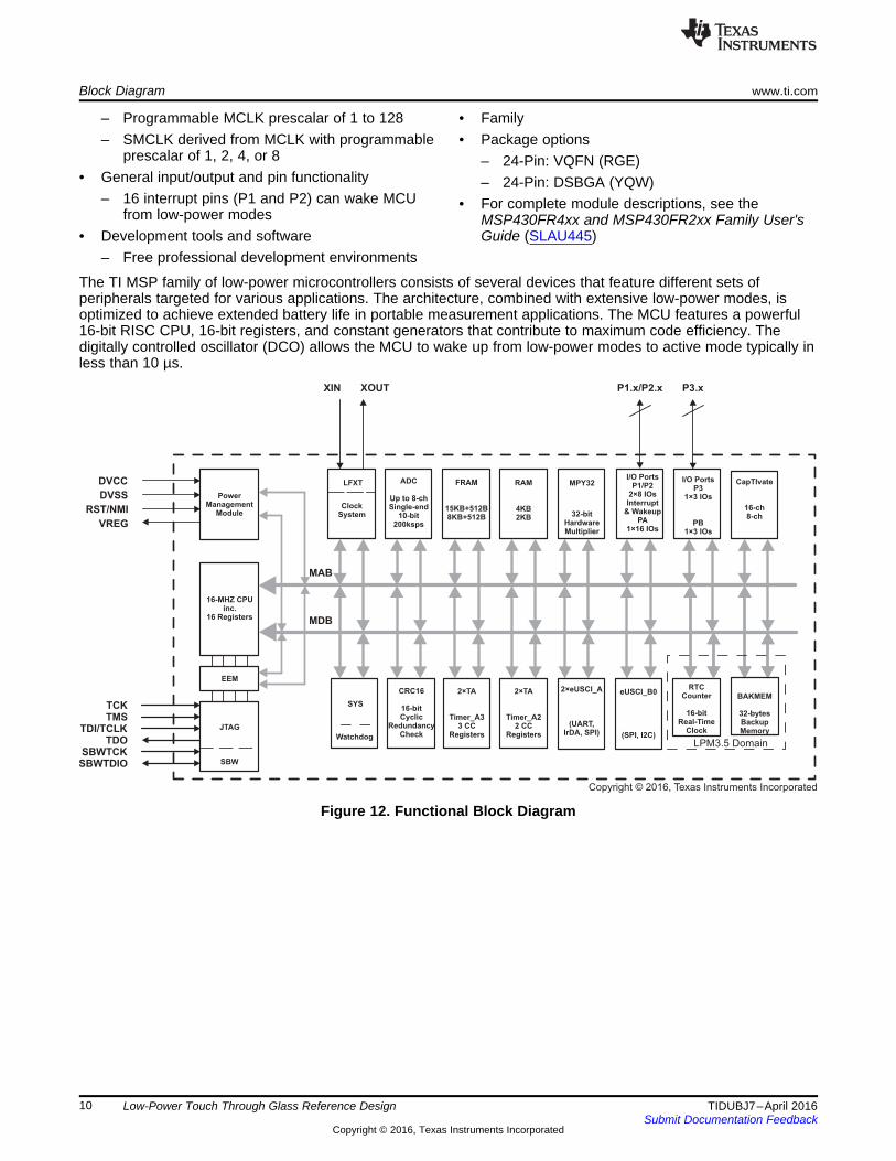
4.1 Highlighted ProductsThe key part of the TIDA-00343 system design is the MSP430FR2633 MCU, which allows capacitivesensing by pressing a button. The touch of this button registers, even through layers, such as a screen ofthick glass. The implementation of CapTIvate technology enables the capacitive touch sensing capabilitiesof the MSP430FR2633 MCU.
(1) Minimum supply voltage is restricted by SVS levels
4.1.1 MSP430FR2633• Embedded microcontroller
– 16-bit RISC architecture– Clock supports frequencies up to 16 MHz– Wide supply voltage range from 1.8 V to 3.6 V
(1)
• Optimized ultra-low-power modes– Active mode: 126 µA/MHz (typical)– Standby– LPM3.5 real-time clock (RTC) counter with
32768-Hz crystal: 770 nA (typical)– Shutdown (LPM4.5): 15 nA (Typical)
• Low-power ferroelectric RAM (FRAM)– Up to 15.5KB of nonvolatile memory– Built-in error correction code (ECC)– Configurable write protection– Unified memory of program, constants, and
storage– 1015 write cycle endurance– Radiation resistant and nonmagnetic– High FRAM-to-SRAM ratio, up to 4:1.....
.• Intelligent digital peripherals
– Four 16-bit timers• Two timers with three capture/compare
registers each (Timer_A3)• Two timers with two capture/compare
registers each (Timer_A2)– One 16-bit counter-only RTC– 16-bit cyclic redundancy check (CRC)
• Enhanced serial communications– Two enhanced universal serial communication
interfaces (eUSCI_A) support UART, IrDA, andSPI
– One eUSCI (eUSCI_B) supports SPI and I2C• High-performance analog
– 8-channel 10-bit analog-to-digital converter(ADC)• Internal 1.5-V reference
• Clock system (CS)– On-chip 32-kHz RC oscillator (REFO)– On-chip 16-MHz digitally controlled oscillator
(DCO) with frequency-locked loop (FLL)• ±1% accuracy with on-chip reference at
room temperature– On-chip very low-frequency 10-kHz oscillator
(VLO)– On-chip high-frequency modulation oscillator
(MODOSC)– External 32-kHz crystal oscillator (LFXT)
DVCC
RST/NMI
XIN XOUT P3.xP1.x/P2.x
DVSS
I/O PortsP1/P2
2×8 IOsInterrupt
& WakeupPA
1×16 IOs
ADC
Up to 8-chSingle-end
10-bit200ksps
ClockSystem
LFXT FRAM
15KB+512B8KB+ B512
RAM
4KB2KB
Watchdog
SYS
CRC16
16-bitCyclic
RedundancyCheck
CapTIvate
16-ch8-ch
JTAG
SBW
I/O PortsP3
1×3 IOs
PB1×3 IOs
2×TA
Timer_A33 CC
Registers
EEM
MAB
MDB
16-MHZ CPUinc.
16 Registers
PowerManagement
Module
MPY32
32-bitHardwareMultiplier
eUSCI_A
(UART,IrDA, SPI)
2× eUSCI_B0
(SPI, I2C)
RTCCounter
16-bitReal-Time
Clock
2×TA
Timer_A22 CC
Registers
VREG
BAKMEM
32-bytesBackupMemory
LPM3.5 Domain
SBWTDIOSBWTCK
TDOTDI/TCLK
TMSTCK
Copyright © 2016, Texas Instruments Incorporated
Block Diagram www.ti.com
10 TIDUBJ7–April 2016Submit Documentation Feedback
Copyright © 2016, Texas Instruments Incorporated
Low-Power Touch Through Glass Reference Design
– Programmable MCLK prescalar of 1 to 128– SMCLK derived from MCLK with programmable
prescalar of 1, 2, 4, or 8• General input/output and pin functionality
– 16 interrupt pins (P1 and P2) can wake MCUfrom low-power modes
• Development tools and software– Free professional development environments
• Family• Package options
– 24-Pin: VQFN (RGE)– 24-Pin: DSBGA (YQW)
• For complete module descriptions, see theMSP430FR4xx and MSP430FR2xx Family User'sGuide (SLAU445)
The TI MSP family of low-power microcontrollers consists of several devices that feature different sets ofperipherals targeted for various applications. The architecture, combined with extensive low-power modes, isoptimized to achieve extended battery life in portable measurement applications. The MCU features a powerful16-bit RISC CPU, 16-bit registers, and constant generators that contribute to maximum code efficiency. Thedigitally controlled oscillator (DCO) allows the MCU to wake up from low-power modes to active mode typically inless than 10 µs.
Figure 12. Functional Block Diagram

www.ti.com Getting Started Hardware
11TIDUBJ7–April 2016Submit Documentation Feedback
Copyright © 2016, Texas Instruments Incorporated
Low-Power Touch Through Glass Reference Design
5 Getting Started HardwareImplement the following steps to set up the hardware:1. Connect the CapTIvate-FR2633 PCB to the CapTIvate-PGMR PCB. For more information about the
CapTIvate-FR2633 PCB and CapTIvate-PGMR PCB, visit the Hardware section of the CapTIvate™Technology Guide.
2. Connect the electrode board to the CapTIvate-FR2633 board through wires. The following Table 4shows the corresponding connections:
Table 4. Electrode Board to CapTIvate™-FR2633Connections
CONNECTOR ELECTRODEBOARD (J1)
CONNECTOR CapTIvate™-FR2633 (J10)
B1 C1B2 C5B3 C9B4 C13L1 A12L2 A13L3 A14L4 A15
GND A1GND Enclosure
3. Use plastic spacers to elevate the board from the floor up to the glass. The length of the spacersdepends on the used enclosure.
4. Use screws, nuts, spacers, or bumpers to establish a defined air gap between the glass window andthe board.
5. Place the board inside the enclosure with the electrode board facing the glass window, as Figure 14shows.
6. Connect the CapTIvate-PGMR PCB to the PC through a micro-USB cable.

Getting Started Firmware www.ti.com
12 TIDUBJ7–April 2016Submit Documentation Feedback
Copyright © 2016, Texas Instruments Incorporated
Low-Power Touch Through Glass Reference Design
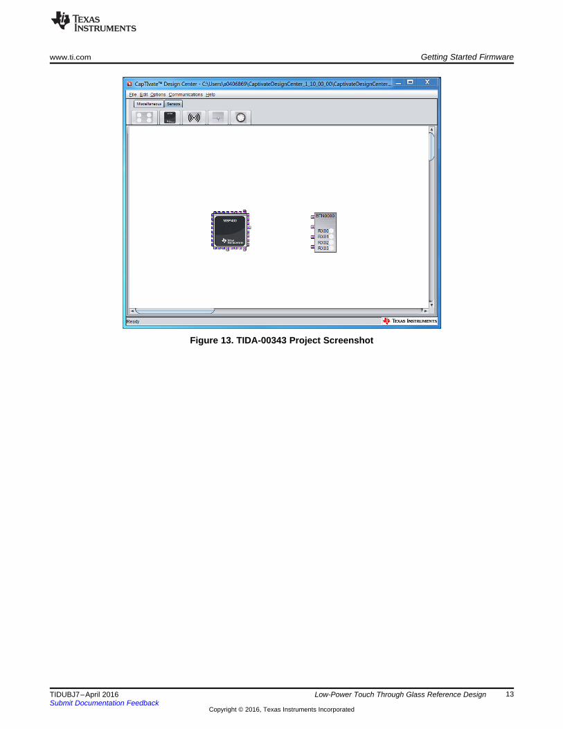
6 Getting Started FirmwareFollow these steps to get started with the firmware (for more information, refer to the Design Center GUIsection of the CapTIvate™ Technology Guide):1. Download the CapTIvate™ Design Center tool.2. Double-click on the desktop shortcut CapTIvateDesignCenter to start the tool.3. In the File menu, navigate to the File → Project New menu to create a new project.4. Place a button group (keypad) sensor in the design area.
(a) Select the button group by clicking on the sensor icon. Place the new object by clicking on thedesign canvas.
5. Display the sensor properties to configure it to be a self-capacitance button group with four elements.(a) Double-click on the button group object in the design area to display its properties.(b) Configure the sensor to have four elements and close the properties dialog by clicking the ok
button.6. Place the MSP430 controller.
(a) Select the MSP430 by clicking on the MCU icon. Place the new object by clicking on the designcanvas.
7. Connect the sensors to the MSP430 capacitive touch input/output (I/O) ports.(a) Double-click on the MSP430 controller object in the design area to display its properties.(b) Configure the MSP430 controller as MSP430FR2633IRHB (32-pin QFN package).(c) Select the Auto-Assign button to automatically assign all the sensor ports to the appropriate ports
on the MSP430.(d) Under the Compile Time Options heading, check the box for Enable Noise Immunity: This option
enables 4-frequency scanning and jitter filtering.8. Generate the source code.
(a) Select the Generate Code button on the MSP430 Controller properties dialog.(b) In the Settings pop-up window for the Select configuration, check the radio button for Create new
project and then click the OK button to create a new full project.(c) In the Settings pop-up window for the Output Directory, click the OK button to keep the default
location for the generated code.9. Load and run the MSP430FR26xx/25xx generated firmware project using the Code Composer
Studio™ (CCS) software from Texas Instruments or IAR.
Figure 13 shows how the CapTIvate Design Center project appears after properly loading:
www.ti.com Getting Started Firmware
13TIDUBJ7–April 2016Submit Documentation Feedback
Copyright © 2016, Texas Instruments Incorporated
Low-Power Touch Through Glass Reference Design
Figure 13. TIDA-00343 Project Screenshot

Test Setup www.ti.com
14 TIDUBJ7–April 2016Submit Documentation Feedback
Copyright © 2016, Texas Instruments Incorporated
Low-Power Touch Through Glass Reference Design
7 Test SetupThe electrode board, CapTIvate-FR2633 PCB, and CapTIvate-PGMR PCB must be connected as outlinedin Section 5 and then contained in an explosive-proof enclosure. A USB wire is the only object that isallowed to protrude from the enclosure and this USB must be connected to a laptop, which uses theCapTIvate Design Center tool to acquire the sensor data. Figure 14 shows an image of the final testsetup.
Figure 14. Test Setup
Adjusting the conversion gain and the conversion count is an important step that the user can control inthe CapTIvate Design Center . Adjust these properties by opening the ButtonGroupSensor properties witha double-click on the button group icon and then navigating to the Conversion_Control tab.
The conversion gain and conversion count are the fundamental parameters used to establish theperformance of the sensor. These parameters determine the resolution, sensitivity, and requiredconversion time.
The TIDA-00343 design has a conversion gain count equal to 1400 and a conversion gain equal to 200.Increasing the strength of the infinite impulse response (IIR) filter to improve the signal-to-noise ratio(SNR) is also possible. This property is controlled by the Count Filter Beta parameter located in the Tuningtab for each sensor. The TIDA-00343 design has a count filter beta set to 3.
The following tests were performed:• Touch• Touch with gloves• False touch
In each test, 1000 samples were taken while pressing a button (touch) and 1000 samples were takenwithout performing any action (untouched). The sampling was followed by a calculation of the SNR andcrosstalk among the buttons.
[ ]( )Sample Size 2
B1 AVG_B10
Untouch_B1
Untouched n Untouched
σSample Size
=
æ ö-ç ÷= ç ÷
ç ÷è ø
ån
[ ]( )Sample Size 2
B1 AVG_B10
Touch_B1
Touched n Touched
σSample Size
=
æ ö-ç ÷= ç ÷
ç ÷è ø
ån
AVG_B1 Touch_B1 AVG_B1 Untouch_B1T 3σ U 3σ> +-
[ ]Sample Size
B10
AVG_B1
Untouched n
UntouchedSample Size
==
ån
[ ]Sample Size
B10
AVG_B1
Touched n
TouchedSample Size
==
ån
UntouchAVG, B1 TouchAVG, B1TS
1Untouch, B1 1Touch, B1
±31Touch, B1 +31Untouch,B1
www.ti.com Test Setup
15TIDUBJ7–April 2016Submit Documentation Feedback
Copyright © 2016, Texas Instruments Incorporated
Low-Power Touch Through Glass Reference Design
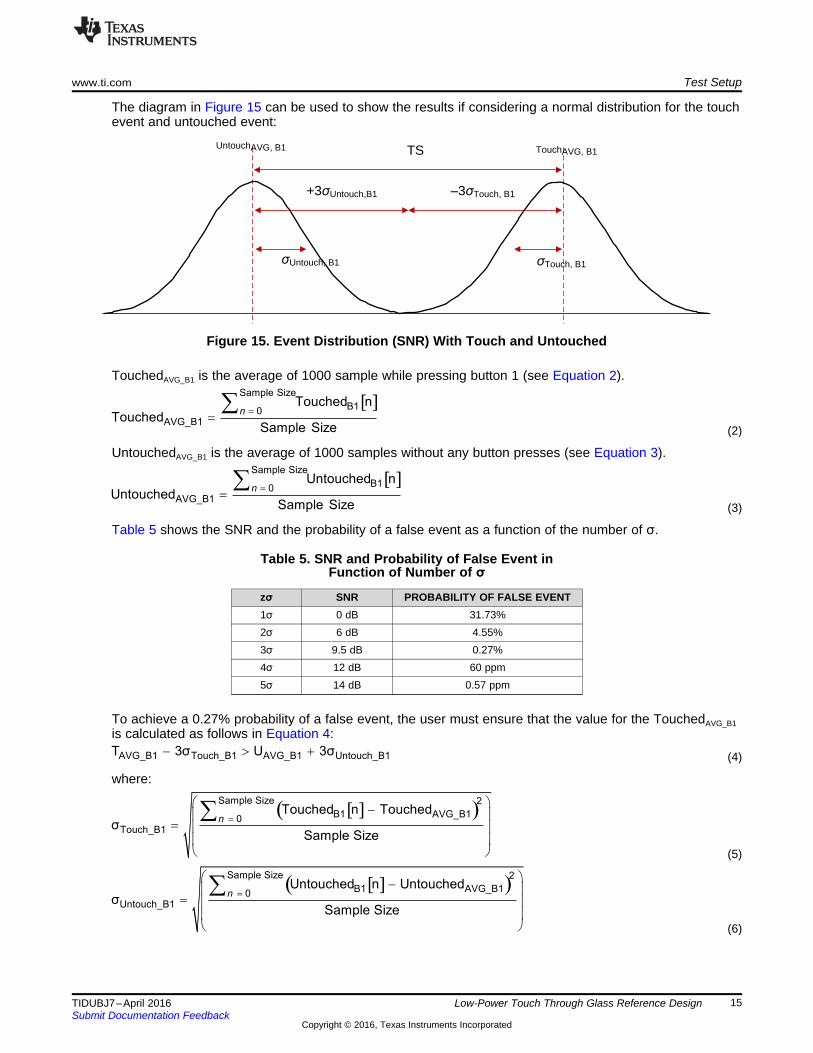
The diagram in Figure 15 can be used to show the results if considering a normal distribution for the touchevent and untouched event:
Figure 15. Event Distribution (SNR) With Touch and Untouched
TouchedAVG_B1 is the average of 1000 sample while pressing button 1 (see Equation 2).
(2)
UntouchedAVG_B1 is the average of 1000 samples without any button presses (see Equation 3).
(3)
Table 5 shows the SNR and the probability of a false event as a function of the number of σ.
Table 5. SNR and Probability of False Event inFunction of Number of σ
zσ SNR PROBABILITY OF FALSE EVENT1σ 0 dB 31.73%2σ 6 dB 4.55%3σ 9.5 dB 0.27%4σ 12 dB 60 ppm5σ 14 dB 0.57 ppm
To achieve a 0.27% probability of a false event, the user must ensure that the value for the TouchedAVG_B1is calculated as follows in Equation 4:
(4)
where:
(5)
(6)

( ) ( )B1_B2
Untouch_B2 Touch_B1
Touch Strength TSCross
σtalk dB 20 log 9
σ.5 dB
æ ö= ´ >ç ÷ç ÷+è ø
UntouchAVG, B2 TouchAVG, B1TS
1Untouch, B2 1Touch, B1
±31Touch, B1 +31Untouch,B2
( ) ( )Untouch_B1 Touch_B1
Touch Strength TSSNR dB 20 log 9
σ.5 B
σd
æ ö= ´ >ç ÷ç ÷+è ø
( ) AVG_B1 AVG_B1Touch Strength TS Untouched Touched= -
( )Untouch_B1 Touch_BAVG_B1 AVG_B1
AVG_B1 AVG 1Unt
_Bouch_B1 Touc B1
1h_
σT U
T U σσ σ
3 3-
- > ®+
>+
Test Setup www.ti.com
16 TIDUBJ7–April 2016Submit Documentation Feedback
Copyright © 2016, Texas Instruments Incorporated
Low-Power Touch Through Glass Reference Design
The calculations from Equation 4 can be further simplified in Equation 7:
(7)
Define the touch strength (TS) in Equation 8 using the previous calculations from Equation 7:
(8)
Calculate the SNR in dB in Equation 9:
(9)
To ensure that the probability of a button being touched is equal to 99.73%, the SNR must be greater than9.5 dB (see Table 5).
The method for calculating the crosstalk is similar to that of the SNR; however, this method considers theaverage of 1000 samples of a button while touching a nearby button (see Figure 16).
Figure 16. Event Distribution (Crosstalk) With Touch and Untouched
In Figure 16, TouchAVG_B1 is equal to the average of 1000 samples while button 1 is pressed andUntouchAVG_B2 is equal to the average of 1000 samples of button 2 while button 1 is pressed.
Equation 10 shows how to calculate the crosstalk:
(10)
To ensure that the probability of an unintentional button touch is equal to 0.27%, the crosstalk must begreater than 9.5 dB (see Figure 16). Refer to Equation 5, Equation 6, and Equation 8 for calculating thetouch strength, σUntouch_B2, and σUntouch_B1.
The air gap between the glass window and the buttons varies in each test from 1 mm to 2 mm and no airgap. Decrease the proximity and touch threshold in the Tuning tab of the ButtonGroupSensor propertiesas the air gap increases.
Air Gap (mm)
SN
R (
dB)
0 0.5 1 1.5 20
5
10
15
20
25
30
35
40
D001
B1B2B3B4
www.ti.com Test Data
17TIDUBJ7–April 2016Submit Documentation Feedback
Copyright © 2016, Texas Instruments Incorporated
Low-Power Touch Through Glass Reference Design
8 Test Data
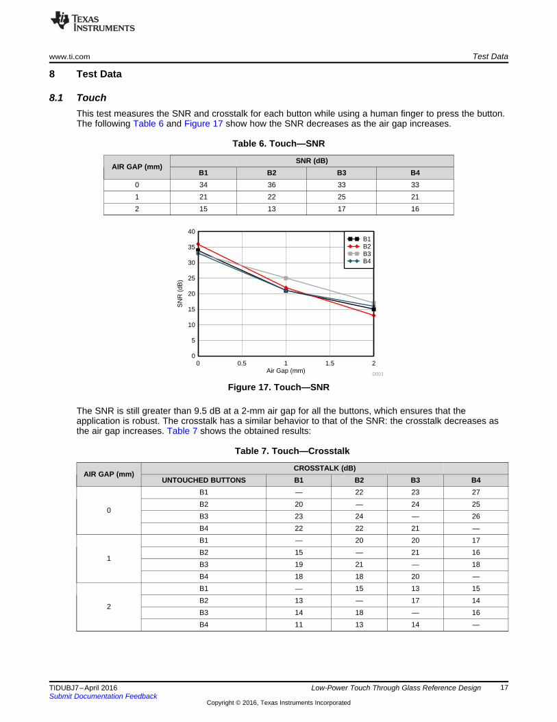
8.1 TouchThis test measures the SNR and crosstalk for each button while using a human finger to press the button.The following Table 6 and Figure 17 show how the SNR decreases as the air gap increases.
Table 6. Touch—SNR
AIR GAP (mm)SNR (dB)
B1 B2 B3 B40 34 36 33 331 21 22 25 212 15 13 17 16
Figure 17. Touch—SNR
The SNR is still greater than 9.5 dB at a 2-mm air gap for all the buttons, which ensures that theapplication is robust. The crosstalk has a similar behavior to that of the SNR: the crosstalk decreases asthe air gap increases. Table 7 shows the obtained results:
Table 7. Touch—Crosstalk
AIR GAP (mm)CROSSTALK (dB)
UNTOUCHED BUTTONS B1 B2 B3 B4
0
B1 — 22 23 27B2 20 — 24 25B3 23 24 — 26B4 22 22 21 —
1
B1 — 20 20 17B2 15 — 21 16B3 19 21 — 18B4 18 18 20 —
2
B1 — 15 13 15B2 13 — 17 14B3 14 18 — 16B4 11 13 14 —

Air Gap(mm)
Cro
ss T
alk
(dB
)
0 0.5 1 1.5 20
5
10
15
20
25
30
35
40
D002
B1vsB2B1vsB3B1vsB4
B2vsB1B2vsB3B2vsB4
B3vsB1B3vsB2B3vsB4
B4vsB1B4vsB2B4vsB3
Test Data www.ti.com
18 TIDUBJ7–April 2016Submit Documentation Feedback
Copyright © 2016, Texas Instruments Incorporated
Low-Power Touch Through Glass Reference Design
The crosstalk is measured for each button pressed. The best crosstalk results are obtained betweenbutton 3 and button 2 because they have the most distance between each other with respect to the otherbuttons (see Figure 5).
Figure 18 shows the crosstalk results:
Figure 18. Touch—Crosstalk
8.2 Touch With GlovesThis test measures the SNR and crosstalk for each button while a human finger wearing a thick glove isused to press the button (see Figure 19).
Figure 19. Example Firefighting Glove
This test shows a significant decrease in the measured SNR and crosstalk in comparison to the testresults without a glove, which is a result of the thick fabric of the glove and its resistance to harshenvironments.
However, the SNR values are still greater than 9.5 dB, even at 2 mm (see Table 8), which indicates thatthe TIDA-00343 device is still capable of recognizing a button press while a user is wearing a thick pair ofgloves (see Figure 20).
Table 8. Touch With Gloves—SNR
AIR GAP (mm)SNR (dB)
B1 B2 B3 B40 24 23 25 231 16 17 19 172 12 14 15 13
Air Gap(mm)
Cro
ss T
alk
(dB
)
0 0.5 1 1.5 20
5
10
15
20
25
30
35
40
D004
B1vsB2B1vsB3B1vsB4
B2vsB1B2vsB3B2vsB4
B3vsB1B3vsB2B3vsB4
B4vsB1B4vsB2B4vsB3
Air Gap (mm)
SN
R (
dB)
0 0.5 1 1.5 20
5
10
15
20
25
30
D003
B1B2B3B4
www.ti.com Test Data
19TIDUBJ7–April 2016Submit Documentation Feedback
Copyright © 2016, Texas Instruments Incorporated
Low-Power Touch Through Glass Reference Design
Figure 20. Touch With Gloves—SNR
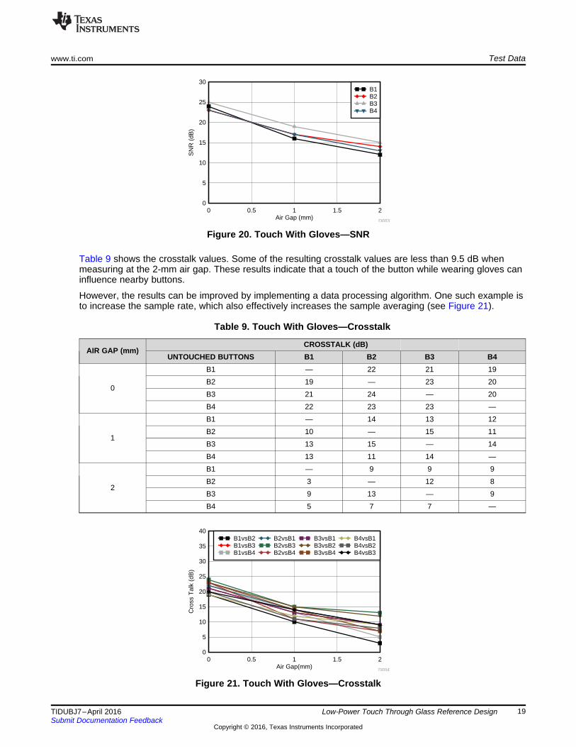
Table 9 shows the crosstalk values. Some of the resulting crosstalk values are less than 9.5 dB whenmeasuring at the 2-mm air gap. These results indicate that a touch of the button while wearing gloves caninfluence nearby buttons.
However, the results can be improved by implementing a data processing algorithm. One such example isto increase the sample rate, which also effectively increases the sample averaging (see Figure 21).
Table 9. Touch With Gloves—Crosstalk
AIR GAP (mm)CROSSTALK (dB)
UNTOUCHED BUTTONS B1 B2 B3 B4
0
B1 — 22 21 19B2 19 — 23 20B3 21 24 — 20B4 22 23 23 —
1
B1 — 14 13 12B2 10 — 15 11B3 13 15 — 14B4 13 11 14 —
2
B1 — 9 9 9B2 3 — 12 8B3 9 13 — 9B4 5 7 7 —
Figure 21. Touch With Gloves—Crosstalk

Groundedmetalenclosure
10-mmthick glass
38
80
1
2
4
3
All measurements are in mm
15.8
11.48.9
13
Test Data www.ti.com
20 TIDUBJ7–April 2016Submit Documentation Feedback
Copyright © 2016, Texas Instruments Incorporated
Low-Power Touch Through Glass Reference Design
8.3 False TouchThis test measures the SNR of the two buttons that are the closest to the false touch position and isperformed by touching the point between two buttons, as Figure 22 shows.
Figure 22. False Touch Example
Table 10 shows the results of the false touch test:
Table 10. False Touch—SNR
AIR GAP (mm)SNR (dB)
B1–B2 B2–B4 B4–B3 B3–B1 B3–B20 24–25 25–21 25–25 26–24 25–211 16–18 19–18 18–19 16–16 17–172 7–7 9–9 10–9 7–10 10–10
In the false touch example, the measured SNR on button 1 and button 2 is 16 dB and 18 dB, respectively,when measuring with a 1-mm air gap. These values show that the SNR of button 1 and button 2 is lowerduring a false-touch event in comparison to the values in Table 6 during a normal button touch event. Theminimum SNR difference between a false and true event is 3 dB. This difference is enough to set a properthreshold to exclude the false touch event from the true event. Another way to address false touch eventsis to exclude them from the true events when the SNR of the two buttons is simultaneously high.
The same false touch test has been performed while wearing the firefighter glove, for which Table 11shows the results.
Table 11. False Touch With Gloves—SNR
AIR GAP (mm)SNR (dB)
B1–B2 B2–B4 B4–B3 B3–B1 B3–B20 17–18 16–17 18–21 19–17 19–161 11–10 13–13 13–16 15–12 12–132 0–7 7–7 3–6 0–5 2–7

www.ti.com Design Files
21TIDUBJ7–April 2016Submit Documentation Feedback
Copyright © 2016, Texas Instruments Incorporated
Low-Power Touch Through Glass Reference Design
9 Design Files
9.1 SchematicsTo download the schematics, see the design files at TIDA-00343.
9.2 Bill of MaterialsTo download the bill of materials (BOM), see the design files at TIDA-00343.
9.3 Layout Guidelines
9.3.1 PCB Layout RecommendationsThe use of a hatched ground plane on the bottom side reduces the parasitic capacitance associated withboth trace and electrode capacitance, reducing the susceptibility of the traces to capacitive touch events(see Figure 23).
Figure 23. TIDA-00343 Layout
TI recommends to keep the traces as short as possible. Increasing the distance of the trace increases theparasitic capacitance associated with the trace. Increasing the trace length can also increase susceptibilityto noise.
Refer to the Best Practices section of the CapTIvate™ Technology Guide to browse otherrecommendations for an optimized layout.
9.4 Layout PrintsTo download the layer plots, see the design files at TIDA-00343.
9.5 Altium ProjectTo download the Altium project files, see the design files at TIDA-00343.

Design Files www.ti.com
22 TIDUBJ7–April 2016Submit Documentation Feedback
Copyright © 2016, Texas Instruments Incorporated
Low-Power Touch Through Glass Reference Design
9.6 Gerber FilesTo download the Gerber files, see the design files at TIDA-00343.
9.7 Assembly DrawingsTo download the assembly drawings, see the design files at TIDA-00343.
10 Software FilesTo download the software files, see the design files at TIDA-00343.
11 References
1. Texas Instruments, CapTIvate™ Technology Guide, Software Guide v1.10.00.00 (http://software-dl.ti.com/msp430/msp430_public_sw/mcu/msp430/CapTIvate_Design_Center/latest/exports/docs/users_guide/html/)
12 About the AuthorGIOVANNI CAMPANELLA is an Industrial Systems Engineer with the Field Transmitter Team in theFactory Automation and Control organization. He earned his bachelor's degree in electronic andtelecommunication engineering at the University of Bologna and his master's degree in electronicengineering at the Polytechnic of Turin in Italy. His design experience covers sensors and analog signalchain (with a focus on fluxgate and analytics sensing technologies) and mixed-signal control of DCbrushed servo drives.
IMPORTANT NOTICE FOR TI REFERENCE DESIGNS
Texas Instruments Incorporated ("TI") reference designs are solely intended to assist designers (“Buyers”) who are developing systems thatincorporate TI semiconductor products (also referred to herein as “components”). Buyer understands and agrees that Buyer remainsresponsible for using its independent analysis, evaluation and judgment in designing Buyer’s systems and products.TI reference designs have been created using standard laboratory conditions and engineering practices. TI has not conducted anytesting other than that specifically described in the published documentation for a particular reference design. TI may makecorrections, enhancements, improvements and other changes to its reference designs.Buyers are authorized to use TI reference designs with the TI component(s) identified in each particular reference design and to modify thereference design in the development of their end products. HOWEVER, NO OTHER LICENSE, EXPRESS OR IMPLIED, BY ESTOPPELOR OTHERWISE TO ANY OTHER TI INTELLECTUAL PROPERTY RIGHT, AND NO LICENSE TO ANY THIRD PARTY TECHNOLOGYOR INTELLECTUAL PROPERTY RIGHT, IS GRANTED HEREIN, including but not limited to any patent right, copyright, mask work right,or other intellectual property right relating to any combination, machine, or process in which TI components or services are used.Information published by TI regarding third-party products or services does not constitute a license to use such products or services, or awarranty or endorsement thereof. Use of such information may require a license from a third party under the patents or other intellectualproperty of the third party, or a license from TI under the patents or other intellectual property of TI.TI REFERENCE DESIGNS ARE PROVIDED "AS IS". TI MAKES NO WARRANTIES OR REPRESENTATIONS WITH REGARD TO THEREFERENCE DESIGNS OR USE OF THE REFERENCE DESIGNS, EXPRESS, IMPLIED OR STATUTORY, INCLUDING ACCURACY ORCOMPLETENESS. TI DISCLAIMS ANY WARRANTY OF TITLE AND ANY IMPLIED WARRANTIES OF MERCHANTABILITY, FITNESSFOR A PARTICULAR PURPOSE, QUIET ENJOYMENT, QUIET POSSESSION, AND NON-INFRINGEMENT OF ANY THIRD PARTYINTELLECTUAL PROPERTY RIGHTS WITH REGARD TO TI REFERENCE DESIGNS OR USE THEREOF. TI SHALL NOT BE LIABLEFOR AND SHALL NOT DEFEND OR INDEMNIFY BUYERS AGAINST ANY THIRD PARTY INFRINGEMENT CLAIM THAT RELATES TOOR IS BASED ON A COMBINATION OF COMPONENTS PROVIDED IN A TI REFERENCE DESIGN. IN NO EVENT SHALL TI BELIABLE FOR ANY ACTUAL, SPECIAL, INCIDENTAL, CONSEQUENTIAL OR INDIRECT DAMAGES, HOWEVER CAUSED, ON ANYTHEORY OF LIABILITY AND WHETHER OR NOT TI HAS BEEN ADVISED OF THE POSSIBILITY OF SUCH DAMAGES, ARISING INANY WAY OUT OF TI REFERENCE DESIGNS OR BUYER’S USE OF TI REFERENCE DESIGNS.TI reserves the right to make corrections, enhancements, improvements and other changes to its semiconductor products and services perJESD46, latest issue, and to discontinue any product or service per JESD48, latest issue. Buyers should obtain the latest relevantinformation before placing orders and should verify that such information is current and complete. All semiconductor products are soldsubject to TI’s terms and conditions of sale supplied at the time of order acknowledgment.TI warrants performance of its components to the specifications applicable at the time of sale, in accordance with the warranty in TI’s termsand conditions of sale of semiconductor products. Testing and other quality control techniques for TI components are used to the extent TIdeems necessary to support this warranty. Except where mandated by applicable law, testing of all parameters of each component is notnecessarily performed.TI assumes no liability for applications assistance or the design of Buyers’ products. Buyers are responsible for their products andapplications using TI components. To minimize the risks associated with Buyers’ products and applications, Buyers should provideadequate design and operating safeguards.Reproduction of significant portions of TI information in TI data books, data sheets or reference designs is permissible only if reproduction iswithout alteration and is accompanied by all associated warranties, conditions, limitations, and notices. TI is not responsible or liable forsuch altered documentation. Information of third parties may be subject to additional restrictions.Buyer acknowledges and agrees that it is solely responsible for compliance with all legal, regulatory and safety-related requirementsconcerning its products, and any use of TI components in its applications, notwithstanding any applications-related information or supportthat may be provided by TI. Buyer represents and agrees that it has all the necessary expertise to create and implement safeguards thatanticipate dangerous failures, monitor failures and their consequences, lessen the likelihood of dangerous failures and take appropriateremedial actions. Buyer will fully indemnify TI and its representatives against any damages arising out of the use of any TI components inBuyer’s safety-critical applications.In some cases, TI components may be promoted specifically to facilitate safety-related applications. With such components, TI’s goal is tohelp enable customers to design and create their own end-product solutions that meet applicable functional safety standards andrequirements. Nonetheless, such components are subject to these terms.No TI components are authorized for use in FDA Class III (or similar life-critical medical equipment) unless authorized officers of the partieshave executed an agreement specifically governing such use.Only those TI components that TI has specifically designated as military grade or “enhanced plastic” are designed and intended for use inmilitary/aerospace applications or environments. Buyer acknowledges and agrees that any military or aerospace use of TI components thathave not been so designated is solely at Buyer's risk, and Buyer is solely responsible for compliance with all legal and regulatoryrequirements in connection with such use.TI has specifically designated certain components as meeting ISO/TS16949 requirements, mainly for automotive use. In any case of use ofnon-designated products, TI will not be responsible for any failure to meet ISO/TS16949.IMPORTANT NOTICE
Mailing Address: Texas Instruments, Post Office Box 655303, Dallas, Texas 75265Copyright © 2016, Texas Instruments Incorporated