Low-power quad voltage comparators - Farnell element14 · Low-power quad voltage comparators...
19
This is information on a product in full production. August 2014 DocID2159 Rev 4 1/19 LM139, LM239, LM339 Low-power quad voltage comparators Datasheet - production data Features • Wide single supply voltage range or dual supplies for all devices: +2 to +36 V or ±1 V to ±18 V • Very low supply current (1.1 mA) independent of supply voltage • Low input bias current: 25 nA typ • Low input offset current: ±5 nA typ • Low input offset voltage: ±1 mV typ • Input common-mode voltage range includes ground • Low output saturation voltage: 250 mV typ; (I SINK = 4 mA) • Differential input voltage range equal to the supply voltage • TTL, DTL, ECL, MOS, CMOS compatible outputs Description This family of devices consists of four independent precision-voltage comparators with an offset voltage specification as low as 2 mV maximum for LM339A, LM239A, and LM139A. Each comparator has been designed specifically to operate from a single power supply over a wide range of voltages. Operation from split power supplies is also possible. These comparators also have a unique characteristic in that the input common mode voltage range includes ground even though operated from a single power supply voltage. D SO14 (plastic micropackage) P TSSOP14 (thin shrink small outline package) Q QFN16 3x3 (plastic micropackage) www.st.com
Transcript of Low-power quad voltage comparators - Farnell element14 · Low-power quad voltage comparators...
This is information on a product in full production.
August 2014 DocID2159 Rev 4 1/19
LM139, LM239, LM339
Low-power quad voltage comparators
Datasheet - production data
Features
• Wide single supply voltage range or dual supplies for all devices: +2 to +36 V or ±1 V to ±18 V
• Very low supply current (1.1 mA) independent of supply voltage
• Low input bias current: 25 nA typ
• Low input offset current: ±5 nA typ
• Low input offset voltage: ±1 mV typ
• Input common-mode voltage range includes ground
• Low output saturation voltage: 250 mV typ; (ISINK = 4 mA)
• Differential input voltage range equal to the supply voltage
• TTL, DTL, ECL, MOS, CMOS compatible outputs
Description
This family of devices consists of four independent precision-voltage comparators with an offset voltage specification as low as 2 mV maximum for LM339A, LM239A, and LM139A. Each comparator has been designed specifically to operate from a single power supply over a wide range of voltages. Operation from split power supplies is also possible.
These comparators also have a unique characteristic in that the input common mode voltage range includes ground even though operated from a single power supply voltage.
DSO14
(plastic micropackage)
PTSSOP14
(thin shrink small outline package)
QQFN16 3x3
(plastic micropackage)
www.st.com
Contents LM139, LM239, LM339
2/19 DocID2159 Rev 4
Contents
1 Pin and schematic diagram . . . . . . . . . . . . . . . . . . . . . . . . . . . . . . . . . . . 3
2 Absolute maximum ratings and operating conditions . . . . . . . . . . . . . 4
3 Electrical characteristics . . . . . . . . . . . . . . . . . . . . . . . . . . . . . . . . . . . . . 6
4 Electrical characteristics curves . . . . . . . . . . . . . . . . . . . . . . . . . . . . . . . 8
5 Typical applications . . . . . . . . . . . . . . . . . . . . . . . . . . . . . . . . . . . . . . . . . 9
6 Package information . . . . . . . . . . . . . . . . . . . . . . . . . . . . . . . . . . . . . . . . 12
6.1 SO14 package information . . . . . . . . . . . . . . . . . . . . . . . . . . . . . . . . . . . . 13
6.2 TSSOP14 package information . . . . . . . . . . . . . . . . . . . . . . . . . . . . . . . . 14
6.3 QFN16 3x3 package information . . . . . . . . . . . . . . . . . . . . . . . . . . . . . . . 15
7 Ordering information . . . . . . . . . . . . . . . . . . . . . . . . . . . . . . . . . . . . . . . 17
8 Revision history . . . . . . . . . . . . . . . . . . . . . . . . . . . . . . . . . . . . . . . . . . . 18
DocID2159 Rev 4 3/19
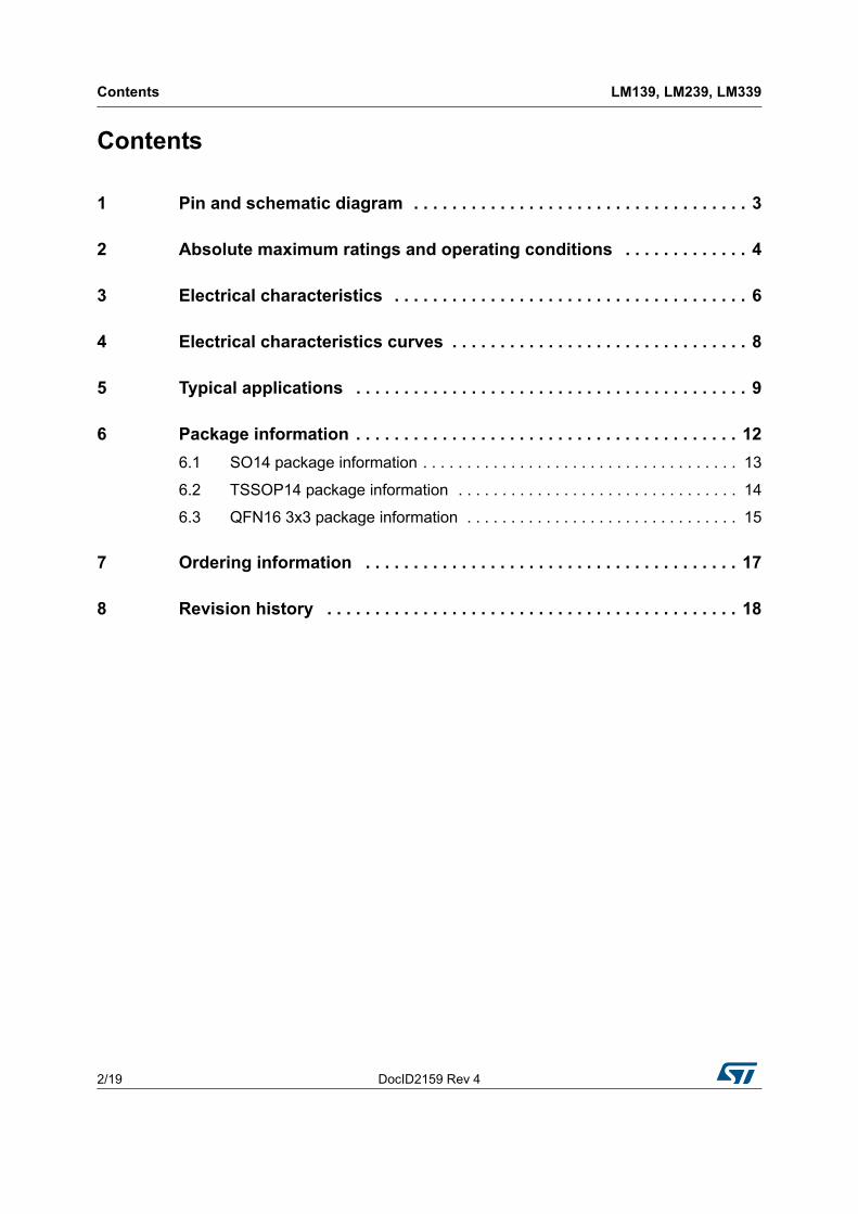
LM139, LM239, LM339 Pin and schematic diagram
19
1 Pin and schematic diagram
Figure 1. Pin connections (top view)
Figure 2. Schematic diagram (1/4 LM139)
4
5
6
7 8
9
10
11
13
1
2
3
14
12
Output2
Output4
Output3
Non-inverting input4
VCC
Non-inverting input3
Inverting input4
VCC
+
Output1
Inverting input1
Non-inverting input2
-
Inverting input3
Non-inverting input1
Inverting input2
Non-invertinginput
Invertinginput
3.5 μA
VCC
VO
3.5 μA 100 μA100 μA
VCC
Absolute maximum ratings and operating conditions LM139, LM239, LM339
4/19 DocID2159 Rev 4
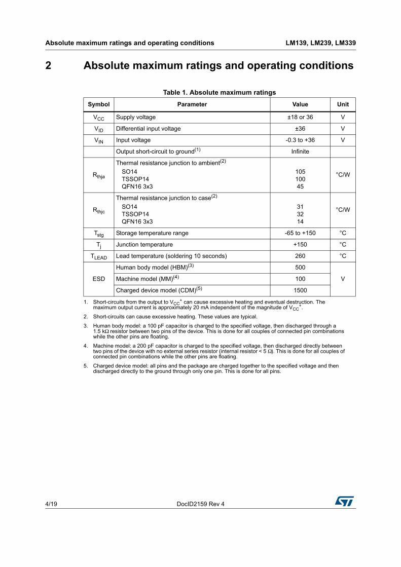
2 Absolute maximum ratings and operating conditions
Table 1. Absolute maximum ratings
Symbol Parameter Value Unit
VCC Supply voltage ±18 or 36 V
VID Differential input voltage ±36 V
VIN Input voltage -0.3 to +36 V
Output short-circuit to ground(1)
1. Short-circuits from the output to VCC+ can cause excessive heating and eventual destruction. The
maximum output current is approximately 20 mA independent of the magnitude of VCC+.
Infinite
Rthja
Thermal resistance junction to ambient(2)
SO14 TSSOP14 QFN16 3x3
2. Short-circuits can cause excessive heating. These values are typical.
10510045
°C/W
Rthjc
Thermal resistance junction to case(2)
SO14 TSSOP14 QFN16 3x3
313214
°C/W
Tstg Storage temperature range -65 to +150 °C
Tj Junction temperature +150 °C
TLEAD Lead temperature (soldering 10 seconds) 260 °C
ESD
Human body model (HBM)(3)
3. Human body model: a 100 pF capacitor is charged to the specified voltage, then discharged through a 1.5 kΩ resistor between two pins of the device. This is done for all couples of connected pin combinations while the other pins are floating.
500
VMachine model (MM)(4)
4. Machine model: a 200 pF capacitor is charged to the specified voltage, then discharged directly between two pins of the device with no external series resistor (internal resistor < 5 Ω). This is done for all couples of connected pin combinations while the other pins are floating.
100
Charged device model (CDM)(5)
5. Charged device model: all pins and the package are charged together to the specified voltage and then discharged directly to the ground through only one pin. This is done for all pins.
1500
DocID2159 Rev 4 5/19
LM139, LM239, LM339 Absolute maximum ratings and operating conditions
19
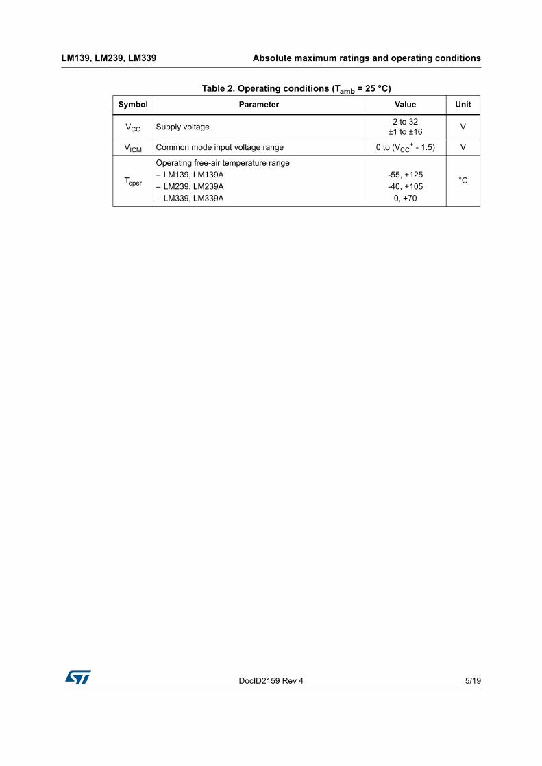
Table 2. Operating conditions (Tamb = 25 °C)
Symbol Parameter Value Unit
VCC Supply voltage2 to 32
±1 to ±16V
VICM Common mode input voltage range 0 to (VCC+ - 1.5) V
Toper
Operating free-air temperature range
– LM139, LM139A
– LM239, LM239A
– LM339, LM339A
-55, +125
-40, +105
0, +70
°C
Electrical characteristics LM139, LM239, LM339
6/19 DocID2159 Rev 4
3 Electrical characteristics
Table 3. Electrical characteristics at VCC+ = +5 V, VCC
- = GND, Tamb = +25 °C (unless otherwise specified)
Symbol Parameter
LM139A - LM239ALM339A
LM139 - LM239LM339 Unit
Min. Typ. Max. Min Typ. Max.
VIOInput offset voltage(1)
Tmin ≤ Tamb ≤ Tmax
1 24
1 59
mV
IIOInput offset current
Tmin ≤ Tamb ≤ Tmax
3 25100
5 50150
nA
IIBInput bias current (I+ or I-)(2)
Tmin ≤ Tamb ≤ Tmax
25 100300
25 250400
nA
AVDLarge signal voltage gain
VCC = 15 V, RL = 15 kΩ, Vo = 1 V to 11 V 50 200 50 200 V/mV
ICC
Supply current (all comparators)
VCC = +5 V, no load VCC = +30 V, no load
1.11.3
22.5
1.11.3
22.5
mA
VICM
Input common mode voltage range(3)
VCC = 30 V
Tmin ≤ Tamb ≤ Tmax
00
VCC+ -1.5
VCC+ -2
00
VCC+ -1.5
VCC+ -2
V
VID Differential input voltage (4) VCC+ VCC
+ V
VOL
Low level output voltage
VID = -1 V, ISINK = 4 mA Tmin ≤ Tamb ≤ Tmax
250 400700
250 400700
mV
IOH
High level output current
VCC = Vo = 30 V, VID = 1 V
Tmin ≤ Tamb ≤ Tmax
0.11
0.11
nAμA
ISINKOutput sink current
VID= 1 V, Vo = 1.5 V 6 16 6 16 mA
treResponse time (5)
RL= 5.1 kΩ connected to VCC+ 1.3 1.3 μs
DocID2159 Rev 4 7/19
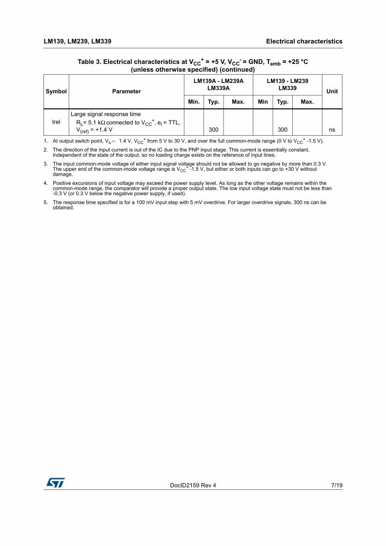
LM139, LM239, LM339 Electrical characteristics
19
trelLarge signal response time
RL= 5.1 kΩ connected to VCC+, el = TTL,
V(ref) = +1.4 V 300 300 ns
1. At output switch point, Vo ≈ 1.4 V, VCC+ from 5 V to 30 V, and over the full common-mode range (0 V to VCC
+ -1.5 V).
2. The direction of the input current is out of the IC due to the PNP input stage. This current is essentially constant, independent of the state of the output, so no loading charge exists on the reference of input lines.
3. The input common-mode voltage of either input signal voltage should not be allowed to go negative by more than 0.3 V. The upper end of the common-mode voltage range is VCC
+ -1.5 V, but either or both inputs can go to +30 V without damage.
4. Positive excursions of input voltage may exceed the power supply level. As long as the other voltage remains within the common-mode range, the comparator will provide a proper output state. The low input voltage state must not be less than -0.3 V (or 0.3 V below the negative power supply, if used).
5. The response time specified is for a 100 mV input step with 5 mV overdrive. For larger overdrive signals, 300 ns can be obtained.
Table 3. Electrical characteristics at VCC+ = +5 V, VCC
- = GND, Tamb = +25 °C (unless otherwise specified) (continued)
Symbol Parameter
LM139A - LM239ALM339A
LM139 - LM239LM339 Unit
Min. Typ. Max. Min Typ. Max.
Electrical characteristics curves LM139, LM239, LM339
8/19 DocID2159 Rev 4
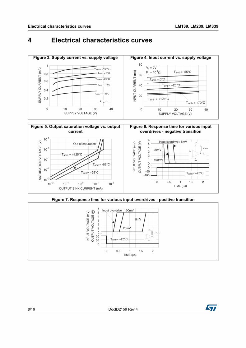
4 Electrical characteristics curves
Figure 7. Response time for various input overdrives - positive transition
Figure 3. Supply current vs. supply voltage Figure 4. Input current vs. supply voltage
SU
PP
LYC
UR
RE
NT
(mA
) 1
0.8
0.6
0.4
0.2
0 10 20 30 40SUPPLY VOLTAGE (V)
Tamb = +70°C
Tamb = +125°C
Tamb = 0°C
R =
Tamb= +25°C
Tamb= -55°C
INP
UT
CU
RR
EN
T(n
A)
20
10 20 30 40SUPPLY VOLTAGE (V)
Tamb = +70°CTamb = +125°C
Tamb= -55°C
40
60
80
0
Tamb = 0°C
Tamb= +25°C
V = 0Vi
R = 10 Ωi
9
Figure 5. Output saturation voltage vs. output current
Figure 6. Response time for various input overdrives - negative transition
Tamb = +125°C
Out of saturation
10 1
10-3
10-2
10 -1
10 0
SA
TU
RA
TIO
NV
OLT
AG
E(V
)
10-2 10 -1 10 0 10 1 10 2
OUTPUT SINK CURRENT (mA)
Out of saturation
Tamb= -55°C
Tamb= +25°C
5V
5.1kΩ
eo
e I
65432
00
-50-100
INP
UT
VO
LTA
GE
(mV
)
OU
TP
UT
VO
LTA
GE
(V)
0 0.5 1 1.5 2TIME (μs)
Input overdrive : 5mV
20mV
1 100mV
Tamb= +25°C
5V
5.1kΩ
eo
e I
6543210
1
0050IN
PU
TV
OLT
AG
E(m
V)
OU
TP
UT
VO
LTA
GE
(V)
0 0.5 1 1.5 2TIME (μs)
0
pIn ut overdrive : 100mV
Tamb= +25°C
5mV
20mV
DocID2159 Rev 4 9/19
LM139, LM239, LM339 Typical applications
19
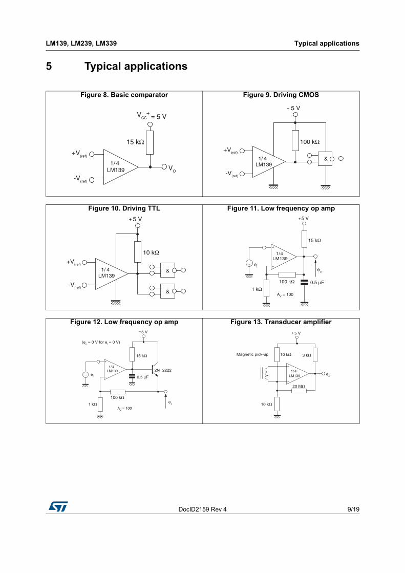
5 Typical applications
Figure 8. Basic comparator Figure 9. Driving CMOS
VCC = 5 V
15 kΩ
VO
+V(ref)
1/4LM139
-V(ref)
5 V
100 kΩ
&1/ 4LM139
+V(ref)
-V(ref)
Figure 10. Driving TTL Figure 11. Low frequency op amp
5 V
10 kΩ+V(ref)
&
&
1/ 4LM139
-V(ref)
5 V
15 kΩ
eo
0.5 μF100 kΩ
el
1 kΩ
~
1/4LM139
AV = 100
Figure 12. Low frequency op amp Figure 13. Transducer amplifier5 V
15 kΩ
0.5 μF
100 kΩ
1 kΩ
~2N 2222
(eo = 0 V for el = 0 V)
1/ 4LM139
eo
el
AV = 100
5 V
10 kΩ
eo
20 MΩ
3 kΩ Magnetic pick-up
10 kΩ
1/ 4LM139
Typical applications LM139, LM239, LM339
10/19 DocID2159 Rev 4
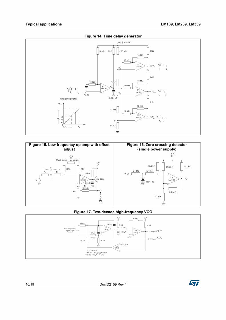
Figure 14. Time delay generator
Figure 17. Two-decade high-frequency VCO
VCC0
V(ref.)
10 kΩ
1/4
15 kΩ 200 kΩ 3 kΩ
3kΩ
3 kΩ
10 MΩ
VO2
V03
O1V
51 kΩ
V1
V2
0.001μF
VC1
V3
VCC
VC1
V1
V2
V3
00 1t t 3t 4t2t
t
VCC
t0
t1
VCC
VCC
VCC = +15V
1/4LM139
1/4
1/4
LM139
LM139
LM139
10 kΩ
10 kΩ
10 kΩ
10 kΩ
10 MΩ
10 MΩ
51 kΩ
51 kΩ
t2
to
t3
to
tA
to
Input gating signal
Figure 15. Low frequency op amp with offset adjust
Figure 16. Zero crossing detector (single power supply)
el~ 2N 2222
5 V
eo
R1100 kΩ
1 kΩ
5 V
1 MΩ
100 kΩ
1 MΩ
Offset adjust
RS R1 15 kΩ
0.5 μF
R2
1/ 4LM139
100 kΩ
10 kΩ
el
20 MΩ
5 V
1N4148
5.1 kΩ
5.1 kΩ100 kΩ
1/ 4LM139
5.1 kΩ
VCC VCC100 kΩ
3 kΩ5.1 kΩ
/2
VCC /2
0.01 μF
500 pF100 kΩ
0.1 μF
20 kΩ
50 kΩ
= + 30 V
+250 mV Vcontrol +50 V
700 Hz f 100 kHzo
20 kΩ
3 kΩ
1/ 4LM139
1/ 4LM139
1/ 4LM139
Output 1
Output 2
VCC
VCC
Frequency controlvoltage input
Vcontrol
DocID2159 Rev 4 11/19
LM139, LM239, LM339 Typical applications
19
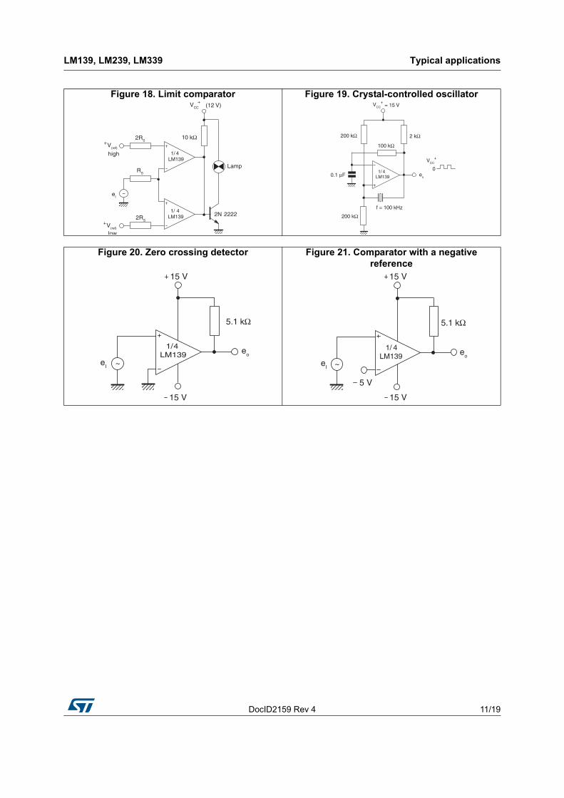
Figure 18. Limit comparator Figure 19. Crystal-controlled oscillator
10 kΩ
eI~
RS
2RS
V(ref)
high
V(ref)
low
2N 2222
VCC
Lamp
1/ 4LM139
1/ 4LM1392RS
(12 V)
2 kΩ
200 kΩ
eo
VCC
0
100 kΩ
200 kΩ
1/ 4LM1390.1 μF
f = 100 kHz
VCC = 15 V
Figure 20. Zero crossing detector Figure 21. Comparator with a negative reference
15 V
5.1 kΩ
eo
eI ~
15 V
1/4LM139
15 V
5.1 kΩ
eo
eI ~
15 V
5 V
1/ 4LM139
Package information LM139, LM239, LM339
12/19 DocID2159 Rev 4
6 Package information
In order to meet environmental requirements, ST offers these devices in different grades of ECOPACK® packages, depending on their level of environmental compliance. ECOPACK® specifications, grade definitions and product status are available at: www.st.com. ECOPACK® is an ST trademark.
DocID2159 Rev 4 13/19
LM139, LM239, LM339 Package information
19
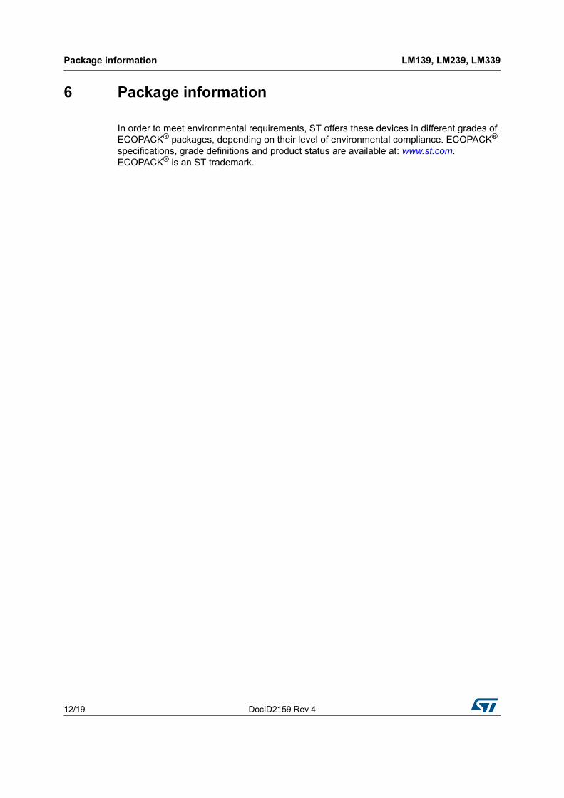
6.1 SO14 package information
Figure 22. SO14 package mechanical drawing
Table 4. SO14 package mechanical data
Dimensions
Ref.Millimeters Inches
Min. Typ. Max. Min. Typ. Max.
A 1.35 1.75 0.05 0.068
A1 0.10 0.25 0.004 0.009
A2 1.10 1.65 0.04 0.06
B 0.33 0.51 0.01 0.02
C 0.19 0.25 0.007 0.009
D 8.55 8.75 0.33 0.34
E 3.80 4.0 0.15 0.15
e 1.27 0.05
H 5.80 6.20 0.22 0.24
h 0.25 0.50 0.009 0.02
L 0.40 1.27 0.015 0.05
k 8° (max.)
ddd 0.10 0.004
Package information LM139, LM239, LM339
14/19 DocID2159 Rev 4
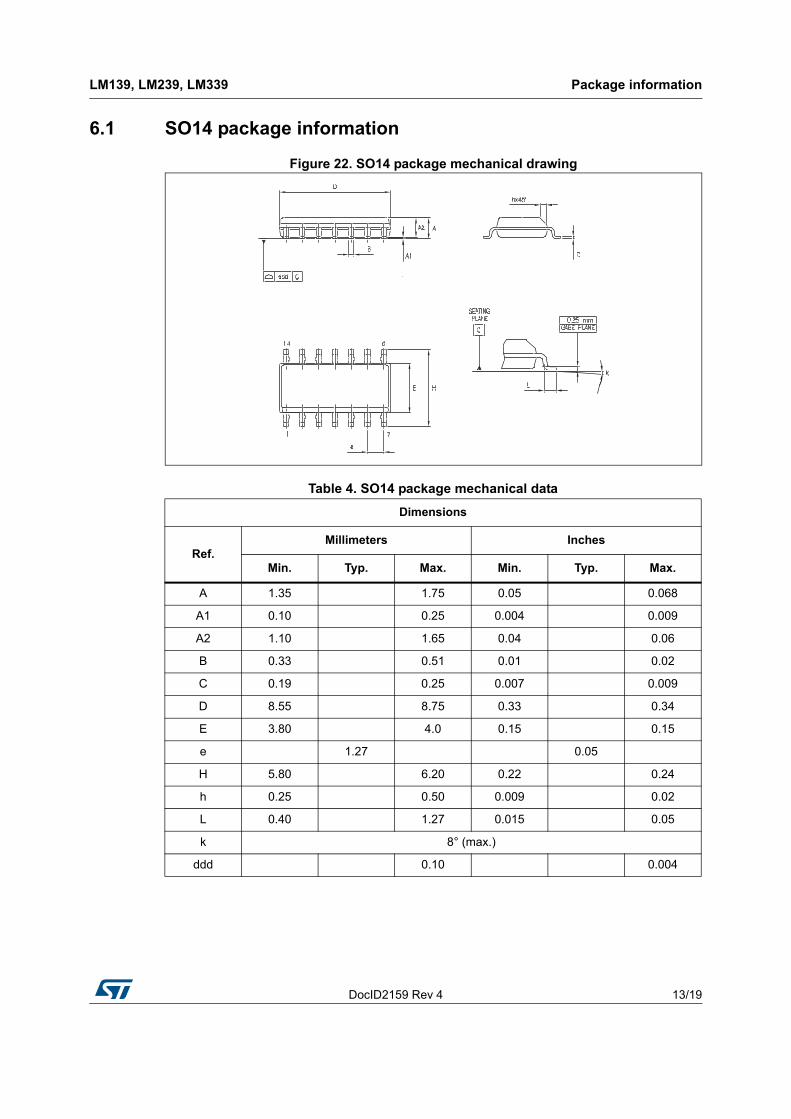
6.2 TSSOP14 package information
Figure 23. TSSOP14 package mechanical drawing
Table 5. TSSOP14 package mechanical data
Ref.
Dimensions
Millimeters Inches
Min. Typ. Max. Min. Typ. Max.
A 1.20 0.047
A1 0.05 0.15 0.002 0.004 0.006
A2 0.80 1.00 1.05 0.031 0.039 0.041
b 0.19 0.30 0.007 0.012
c 0.09 0.20 0.004 0.0089
D 4.90 5.00 5.10 0.193 0.197 0.201
E 6.20 6.40 6.60 0.244 0.252 0.260
E1 4.30 4.40 4.50 0.169 0.173 0.176
e 0.65 0.0256
L 0.45 0.60 0.75 0.018 0.024 0.030
L1 1.00 0.039
k 0° 8° 0° 8°
aaa 0.10 0.004
DocID2159 Rev 4 15/19
LM139, LM239, LM339 Package information
19
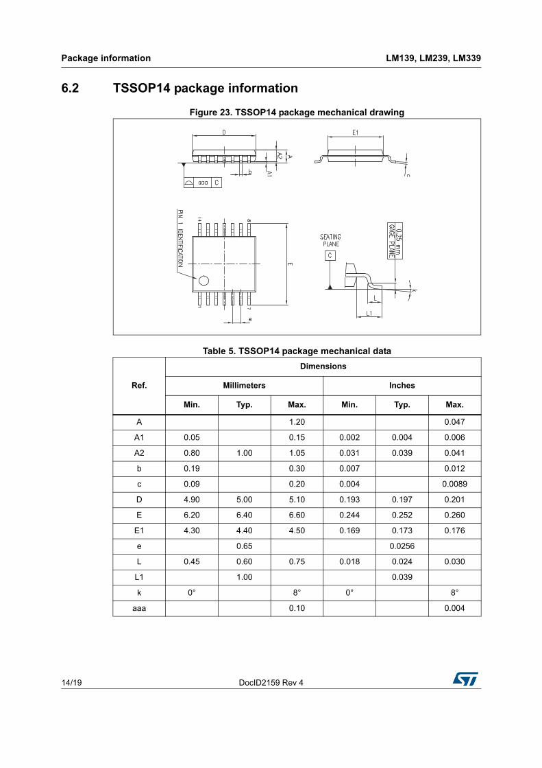
6.3 QFN16 3x3 package information
Figure 24. QFN16 3x3 package mechanical drawing
Package information LM139, LM239, LM339
16/19 DocID2159 Rev 4
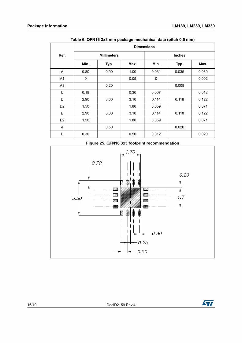
Figure 25. QFN16 3x3 footprint recommendation
Table 6. QFN16 3x3 mm package mechanical data (pitch 0.5 mm)
Ref.
Dimensions
Millimeters Inches
Min. Typ. Max. Min. Typ. Max.
A 0.80 0.90 1.00 0.031 0.035 0.039
A1 0 0.05 0 0.002
A3 0.20 0.008
b 0.18 0.30 0.007 0.012
D 2.90 3.00 3.10 0.114 0.118 0.122
D2 1.50 1.80 0.059 0.071
E 2.90 3.00 3.10 0.114 0.118 0.122
E2 1.50 1.80 0.059 0.071
e 0.50 0.020
L 0.30 0.50 0.012 0.020
DocID2159 Rev 4 17/19
LM139, LM239, LM339 Ordering information
19
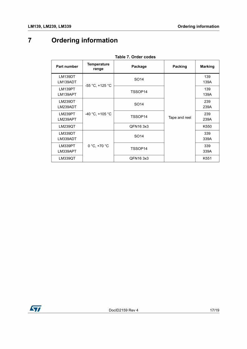
7 Ordering information
Table 7. Order codes
Part numberTemperature
rangePackage Packing Marking
LM139DT
LM139ADT-55 °C, +125 °C
SO14
Tape and reel
139
139A
LM139PT
LM139APTTSSOP14
139
139A
LM239DT
LM239ADT
-40 °C, +105 °C
SO14239
239A
LM239PT
LM239APTTSSOP14
239
239A
LM239QT QFN16 3x3 K550
LM339DT
LM339ADT
0 °C, +70 °C
SO14339
339A
LM339PT
LM339APTTSSOP14
339
339A
LM339QT QFN16 3x3 K551
Revision history LM139, LM239, LM339
18/19 DocID2159 Rev 4
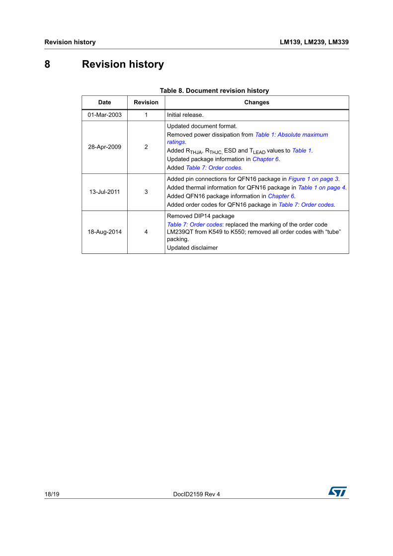
8 Revision history
Table 8. Document revision history
Date Revision Changes
01-Mar-2003 1 Initial release.
28-Apr-2009 2
Updated document format.
Removed power dissipation from Table 1: Absolute maximum ratings.
Added RTHJA, RTHJC, ESD and TLEAD values to Table 1.
Updated package information in Chapter 6.
Added Table 7: Order codes.
13-Jul-2011 3
Added pin connections for QFN16 package in Figure 1 on page 3.
Added thermal information for QFN16 package in Table 1 on page 4.
Added QFN16 package information in Chapter 6.
Added order codes for QFN16 package in Table 7: Order codes.
18-Aug-2014 4
Removed DIP14 package
Table 7: Order codes: replaced the marking of the order code LM239QT from K549 to K550; removed all order codes with “tube” packing.
Updated disclaimer
DocID2159 Rev 4 19/19
LM139, LM239, LM339
19
IMPORTANT NOTICE – PLEASE READ CAREFULLY
STMicroelectronics NV and its subsidiaries (“ST”) reserve the right to make changes, corrections, enhancements, modifications, and improvements to ST products and/or to this document at any time without notice. Purchasers should obtain the latest relevant information on ST products before placing orders. ST products are sold pursuant to ST’s terms and conditions of sale in place at the time of order acknowledgement.
Purchasers are solely responsible for the choice, selection, and use of ST products and ST assumes no liability for application assistance or the design of Purchasers’ products.
No license, express or implied, to any intellectual property right is granted by ST herein.
Resale of ST products with provisions different from the information set forth herein shall void any warranty granted by ST for such product.
ST and the ST logo are trademarks of ST. All other product or service names are the property of their respective owners.
Information in this document supersedes and replaces information previously supplied in any prior versions of this document.
© 2014 STMicroelectronics – All rights reserved