Low Power PL FM Transmitter - Greg · PDF file2.2 Phase-Locked Loop Module “A...
41
Low Power PLL FM Transmitter Greg Browne 200119576
Transcript of Low Power PL FM Transmitter - Greg · PDF file2.2 Phase-Locked Loop Module “A...
Low Power PLL FM
Transmitter
Greg Browne 200119576
TABLE OF CONTENTS
TABLE OF CONTENTS I
ABSTRACT III
1 INTRODUCTION 1
1.1 Auto Slalom Background 1
1.2 Current Communication Setup 2 1.2.1 Photogates 2 1.2.2 Controller & Stopwatch 2 1.2.3 Bullhorn / Common FM Transmitter 3
2 SYSTEM DESIGN 3
2.1 Audio Module 5 2.1.1 Microphone 6 2.1.2 Audio Signal Conditioning 7
2.2 Phase-Locked Loop Module 9 2.2.1 Crystal Oscillator 10 2.2.2 Voltage-Controlled Oscillator (VCO) 12 2.2.3 Frequency Divider 14 2.2.4 Phase Detector 15 2.2.5 Loop Filter 16
2.3 FM Transmitter Module 17 2.3.1 FM Modulator 17 2.3.2 Radio Frequency (RF) Amplifier 19 2.3.3 Antenna 20 2.3.4 Channel Selection 23
2.4 Auxiliary Components 24
3 RESULTS AND RECOMMENDATIONS 26
3.1 Performance Results 26
3.2 Problems / Implementation Issues 27 3.2.1 Microphone Biasing 27
Low Power PLL FM Transmitter I
3.2.2 Immeasurable Inductance 27 3.2.3 Frequency Division 29 3.2.4 RF Infection 29 3.2.5 Recommended Design Improvements 30
4 RESOURCES COST ANALYSIS 33
4.1 Parts List Costing 33
4.2 Equipment and Software 34
5 REFERENCES 35
APPENDIX – LPPFMTX BOARD LAYOUT 37
Low Power PLL FM Transmitter II
ABSTRACT
The Low Power PLL FM Transmitter (LPPFMTx) is a one-way communication system developed for Vinland Motorsports Inc, a local motorsports club. It is to replace the existing method of communication (bullhorn, 2-way radios and/or common FM transmitter) for use during their events, such as auto slalom. The LPPFMTx is a method of broadcasting announcements (via standard microphone input) tunable by a commercial FM radio, which is not prone to the shortcomings of a common FM transmitter. These shortcomings include high power output and long distance transmissions (which violate government anti-piracy regulations), as well as frequency drifting (caused by factors such as thermal instabilities and inertial forces). The above problems are avoided via the phase locked loop (PLL) implementation operating in conjunction with an FM transmitter design. The PLL involves the feedback of the FM output, through a frequency divider, to a phase comparator. The signal is then compared against a stable crystal oscillator to produce a variable-duty error signal to be incident upon the voltage-controlled oscillator (VCO). The VCO frequency will then be adjusted until the system reaches equilibrium and is successfully “locked” to that of the stable crystal. Moreover, the input (voice) signal undergoes high-order Butterworth low-pass filtering in conjunction with power input filtering to maximize the signal-to-noise ratio (SNR) of the system. The result is a clean and clear FM transmission that has the stability of a crystal and the flexibility of a tunable FM transmitter that can be received on the order of 1 km away and is powered via an automotive accessory (cigarette lighter) jack. Supervisors: Dr. Weimin Huang Mr. Andrew Menchions, P. Eng
Low Power PLL FM Transmitter III
1 INTRODUCTION
This project, the Low Power PLL FM Transmitter (LPPFMTx), was designed for
Vinland Motorsports Inc., as suggested by its Auto Slalom Director, Andrew
Menchions. “Vinland Motorsports Inc. (VMI) is an autosport club and a member
of Atlantic Region Motor Sport Club (A.R.M.S.), the Canadian Association of
Rallysport (C.A.R.S.) and affiliated with ASN-Canada-FIA. VMI organizes rallies
and auto slalom events throughout the year and aims to promote all aspects of
autosport in the Province of Newfoundland and Labrador”.[1]
The purpose of the LPPFMTx is to replace the existing rudimentary
communication system with a more sophisticated system available to all
participants and competitors.
1.1 Auto Slalom Background
Auto Slalom is a motorsports event similar to the American “autocross”. “An
autocross is a timed competition where drivers navigate one at a time through a
temporary course marked by traffic cones, rather than racing on a track with
multiple other cars, as in road racing or oval racing. Autocross tends to place
more emphasis on car handling and driver skill than on sheer horsepower, and
events typically have many classes which allow almost any vehicle, from
economy sedans to purpose-built vehicles, to compete. Speeds are slower in
absolute terms when compared to other forms of motorsports, usually not
Low Power PLL FM Transmitter 1
exceeding highway speeds, but the activity level (measured in driver inputs per
second) can be higher than even Formula One due to the large number of
elements packed into each course.”[2]
1.2
1.2.1 Photogates
1.2.2
Current Communication Setup
The current communication setup employed by VMI includes the following:
• Photogates
• Controller & Stopwatch
• Bullhorn / Common FM Transmitter
There are two photogates being utilized by the current communication setup – at
the start gate and stop box. These are triggered when the currently competing
car crosses the plane between the transmitter and receiver.
Controller & Stopwatch
When the first photogate is triggered, the controller activates the stopwatch and
similarly deactivates it upon the triggering of the second photogate. The resulting
time is then recorded in a spreadsheet either manually or on a laptop in the
timing vehicle.
Low Power PLL FM Transmitter 2
1.2.3 Bullhorn / Common FM Transmitter
A bullhorn or common FM transmitter may or may not be used to relay run times
and other announcements. The main purpose of the LPPFMTx is to replace this
element of the current communication setup. When referring to a “common FM
transmitter” in this document, the reference is to any that will cost around $20
and operate in open loop.
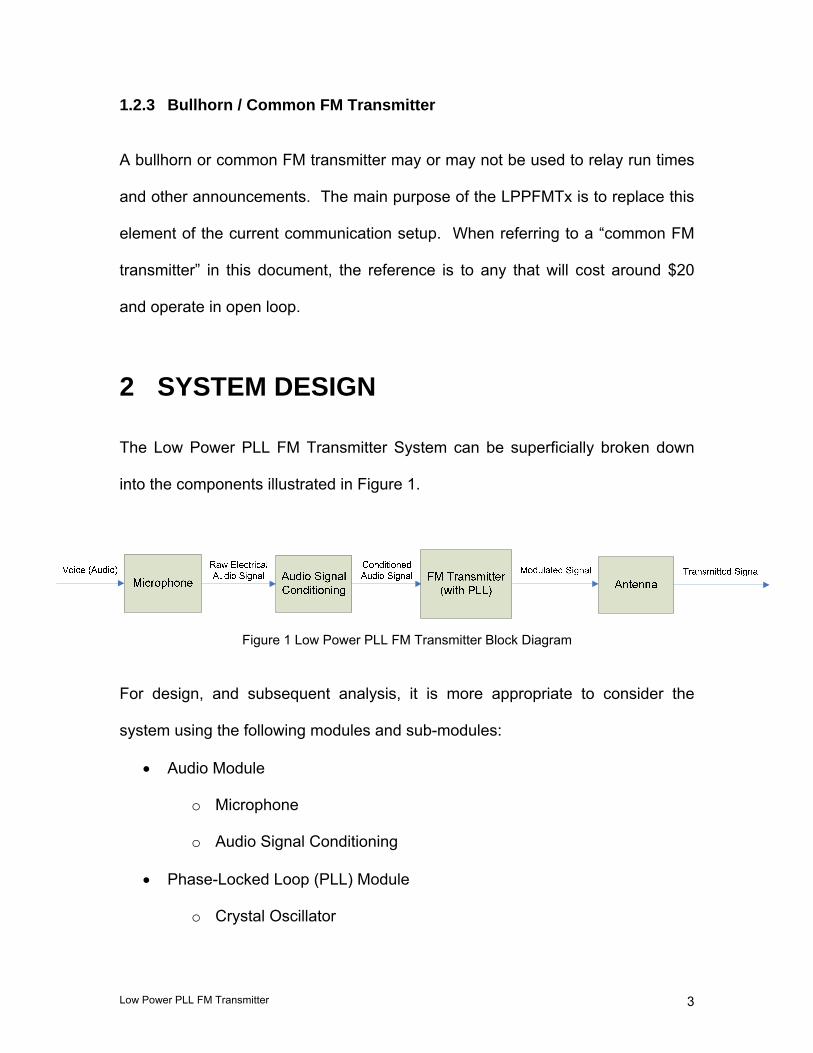
2 SYSTEM DESIGN
The Low Power PLL FM Transmitter System can be superficially broken down
into the components illustrated in Figure 1.
Figure 1 Low Power PLL FM Transmitter Block Diagram
For design, and subsequent analysis, it is more appropriate to consider the
system using the following modules and sub-modules:
• Audio Module
o Microphone
o Audio Signal Conditioning
• Phase-Locked Loop (PLL) Module
o Crystal Oscillator
Low Power PLL FM Transmitter 3
o Voltage-Controlled Oscillator
o Frequency Divider
o Phase Detector
o Loop Filter
• FM Transmitter
o FM Modulator
o RF Amplifier
o Antenna
o Channel Selection
The physical layout of these modules is illustrated in Figure 2. The modules will
be broken down and subsequently discussed throughout this document.
External connectors include:
• 3.5mm jack – microphone input
• Rocker switch – power on/off
• LED – power indicator
• Power jack – power from 12V adapter
• Push button – channel selection
• 4 x LED – channel indicator
• BNC-style connector – Antenna output
Low Power PLL FM Transmitter 4
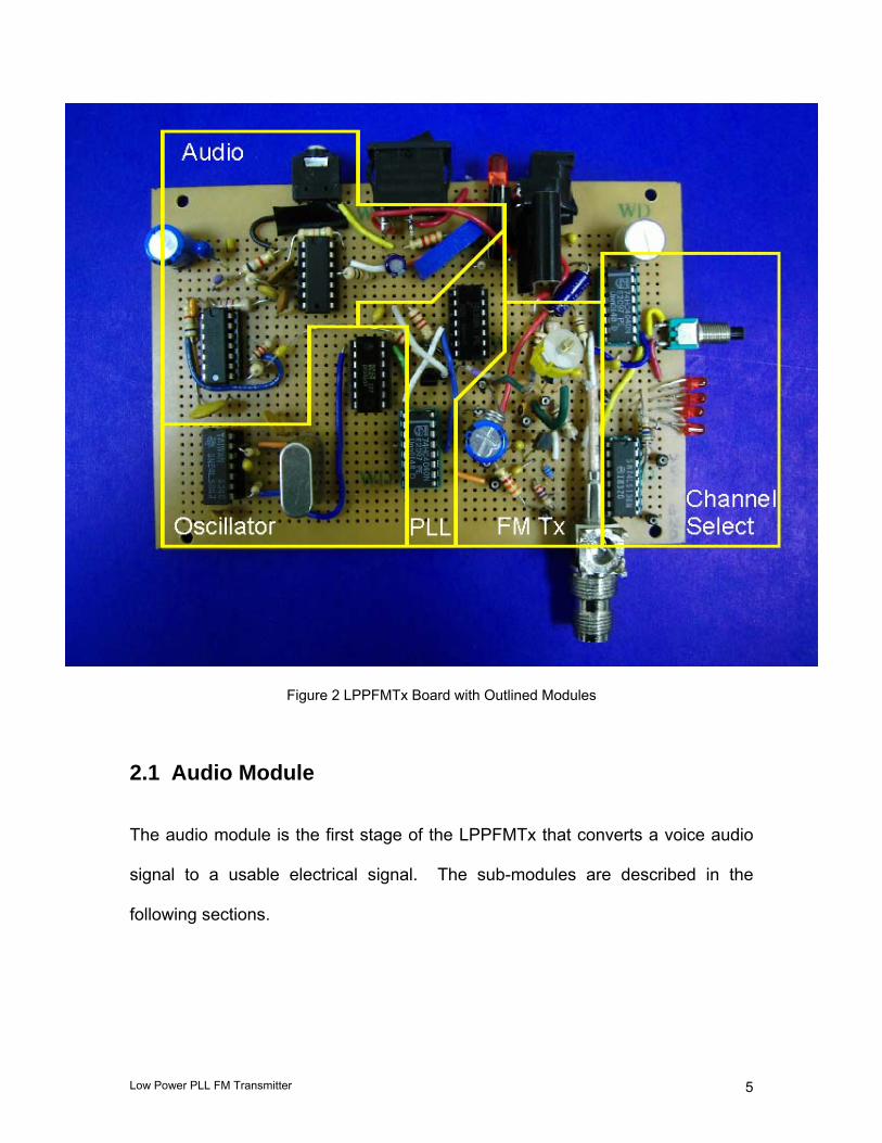
Figure 2 LPPFMTx Board with Outlined Modules
2.1 Audio Module
The audio module is the first stage of the LPPFMTx that converts a voice audio
signal to a usable electrical signal. The sub-modules are described in the
following sections.
Low Power PLL FM Transmitter 5
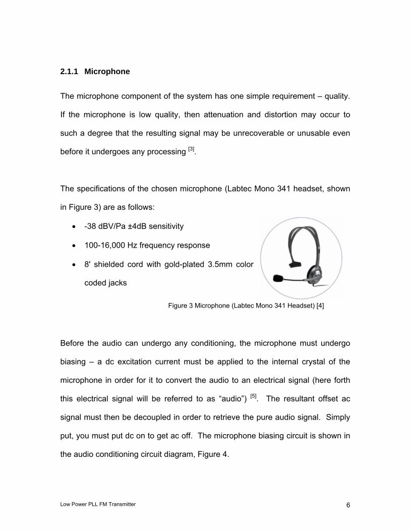
2.1.1 Microphone The microphone component of the system has one simple requirement – quality.
If the microphone is low quality, then attenuation and distortion may occur to
such a degree that the resulting signal may be unrecoverable or unusable even
before it undergoes any processing [3].
The specifications of the chosen microphone (Labtec Mono 341 headset, shown
in Figure 3) are as follows:
• -38 dBV/Pa ±4dB sensitivity
• 100-16,000 Hz frequency response
• 8' shielded cord with gold-plated 3.5mm color
coded jacks
Figure 3 Microphone (Labtec Mono 341 Headset) [4]
Before the audio can undergo any conditioning, the microphone must undergo
biasing – a dc excitation current must be applied to the internal crystal of the
microphone in order for it to convert the audio to an electrical signal (here forth
this electrical signal will be referred to as “audio”) [5]. The resultant offset ac
signal must then be decoupled in order to retrieve the pure audio signal. Simply
put, you must put dc on to get ac off. The microphone biasing circuit is shown in
the audio conditioning circuit diagram, Figure 4.
Low Power PLL FM Transmitter 6
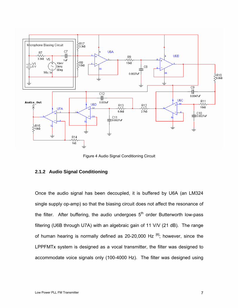
Figure 4 Audio Signal Conditioning Circuit
2.1.2 Audio Signal Conditioning
Once the audio signal has been decoupled, it is buffered by U6A (an LM324
single supply op-amp) so that the biasing circuit does not affect the resonance of
the filter. After buffering, the audio undergoes 5th order Butterworth low-pass
filtering (U6B through U7A) with an algebraic gain of 11 V/V (21 dB). The range
of human hearing is normally defined as 20-20,000 Hz [6]; however, since the
LPPFMTx system is designed as a vocal transmitter, the filter was designed to
accommodate voice signals only (100-4000 Hz). The filter was designed using
Low Power PLL FM Transmitter 7
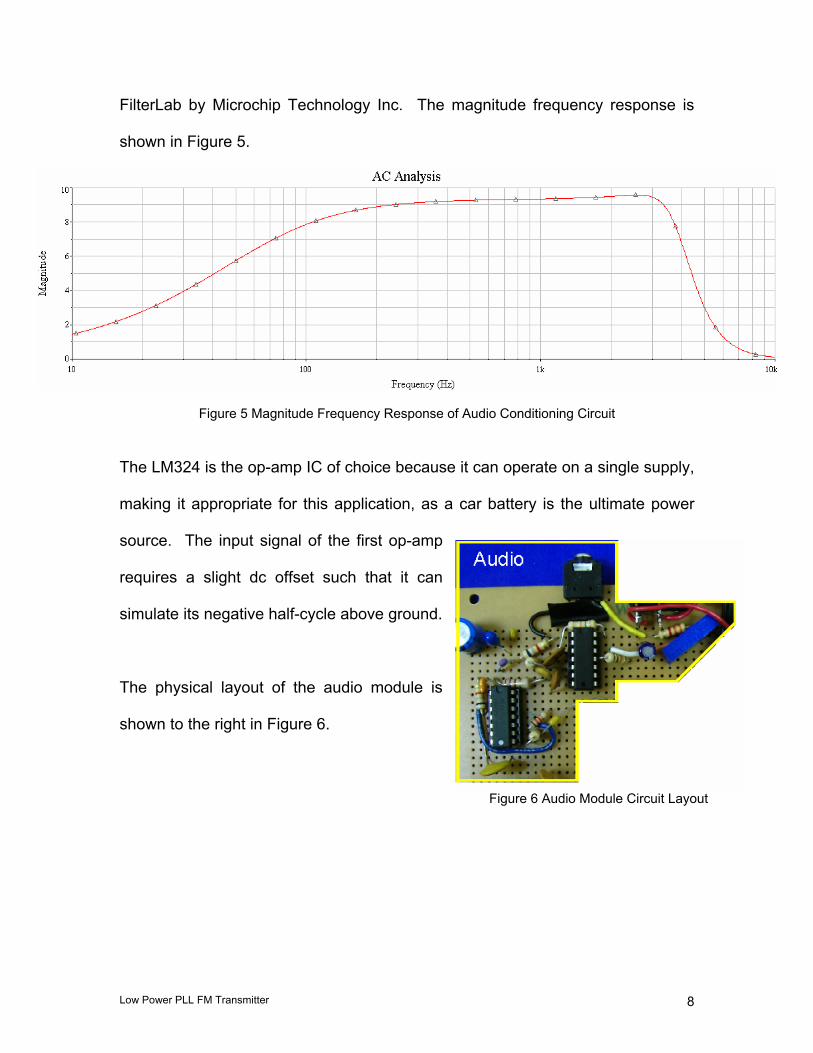
FilterLab by Microchip Technology Inc. The magnitude frequency response is
shown in Figure 5.
Figure 5 Magnitude Frequency Response of Audio Conditioning Circuit
The LM324 is the op-amp IC of choice because it can operate on a single supply,
making it appropriate for this application, as a car battery is the ultimate power
source. The input signal of the first op-amp
requires a slight dc offset such that it can
simulate its negative half-cycle above ground.
The physical layout of the audio module is
shown to the right in Figure 6.
Figure 6 Audio Module Circuit Layout
Low Power PLL FM Transmitter 8
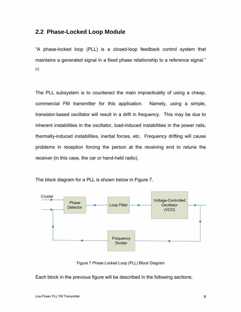
2.2 Phase-Locked Loop Module
“A phase-locked loop (PLL) is a closed-loop feedback control system that
maintains a generated signal in a fixed phase relationship to a reference signal.”
[7]
The PLL subsystem is to counteract the main impracticality of using a cheap,
commercial FM transmitter for this application. Namely, using a simple,
transistor-based oscillator will result in a drift in frequency. This may be due to
inherent instabilities in the oscillator, load-induced instabilities in the power rails,
thermally-induced instabilities, inertial forces, etc. Frequency drifting will cause
problems in reception forcing the person at the receiving end to retune the
receiver (in this case, the car or hand-held radio).
The block diagram for a PLL is shown below in Figure 7.
Phase Detector Loop Filter
Voltage-Controlled Oscillator
(VCO)
FrequencyDivider
Crystal
Figure 7 Phase Locked Loop (PLL) Block Diagram
Each block in the previous figure will be described in the following sections.
Low Power PLL FM Transmitter 9
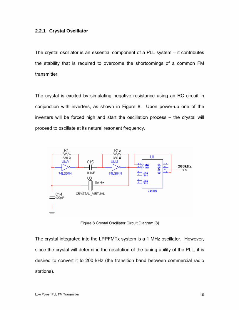
2.2.1 Crystal Oscillator
The crystal oscillator is an essential component of a PLL system – it contributes
the stability that is required to overcome the shortcomings of a common FM
transmitter.
The crystal is excited by simulating negative resistance using an RC circuit in
conjunction with inverters, as shown in Figure 8. Upon power-up one of the
inverters will be forced high and start the oscillation process – the crystal will
proceed to oscillate at its natural resonant frequency.
Figure 8 Crystal Oscillator Circuit Diagram [8]
The crystal integrated into the LPPFMTx system is a 1 MHz oscillator. However,
since the crystal will determine the resolution of the tuning ability of the PLL, it is
desired to convert it to 200 kHz (the transition band between commercial radio
stations).
Low Power PLL FM Transmitter 10
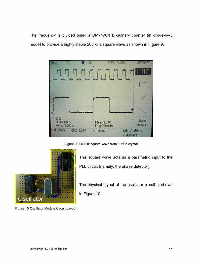
The frequency is divided using a DM7490N Bi-quinary counter (in divide-by-5
mode) to provide a highly stable 200 kHz square wave as shown in Figure 9.
Figure 9 200 kHz square wave from 1 MHz crystal
This square wave acts as a parametric input to the
PLL circuit (namely, the phase detector).
The physical layout of the oscillator circuit is shown
in Figure 10.
Figure 10 Oscillator Module Circuit Layout
Low Power PLL FM Transmitter 11
A crystal cannot (or should not) simply be used as a solution to the stability issue
associated with a common FM transmitter because it cannot be tuned to
resonate at a frequency other than its fundamental.
2.2.2 Voltage-Controlled Oscillator (VCO)
Due to the cyclic nature of the PLL process, its performance is perhaps best
analyzed by starting at the output and working backwards to the “input”. The
most obvious point to consider as the output would be the VCO.
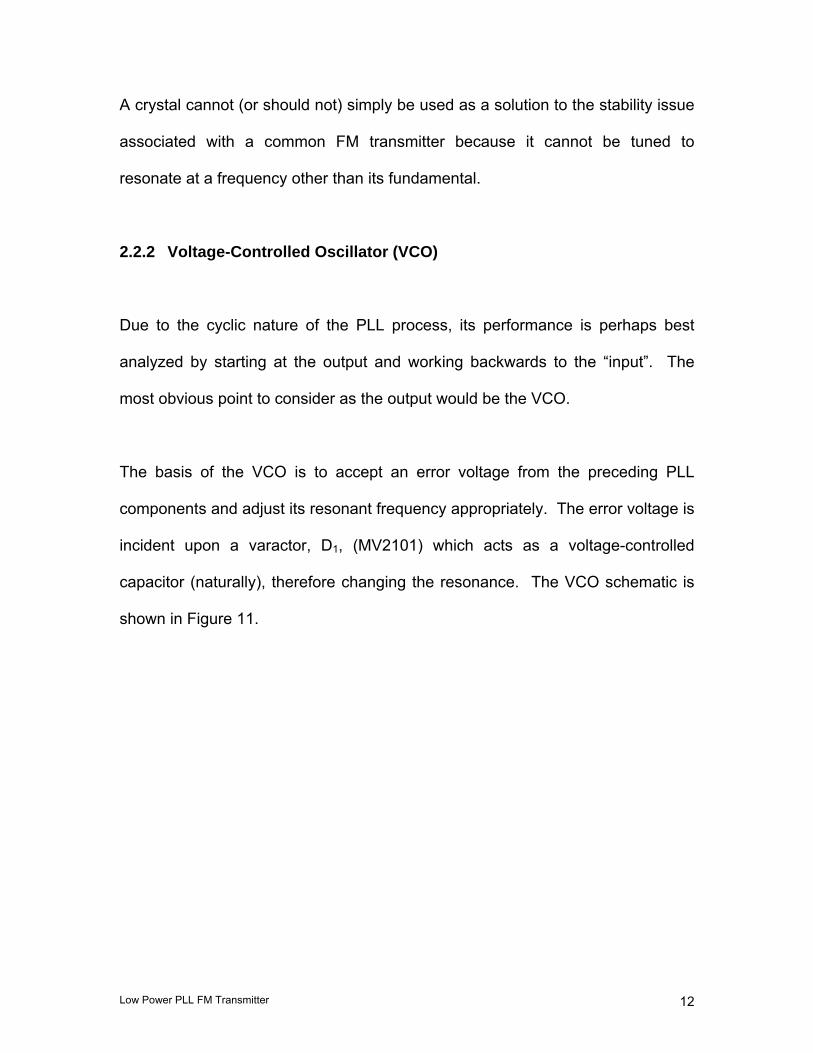
The basis of the VCO is to accept an error voltage from the preceding PLL
components and adjust its resonant frequency appropriately. The error voltage is
incident upon a varactor, D1, (MV2101) which acts as a voltage-controlled
capacitor (naturally), therefore changing the resonance. The VCO schematic is
shown in Figure 11.
Low Power PLL FM Transmitter 12
R110kΩ
R210kΩ
C1
1nF
C227pF
L171nH
V312 V
C4
1nF
C5
10pF R5100kΩ
D1FMMV2101
PD_Out
R6
220 Ω
C6
10nF VCO_Out
Audio_Out
U17150 Ω
U1815 Ω
C3Key = A 78pF 50%
Q1
PN2222A
Figure 11 VCO / FM Modulator Schematic
The oscillator is based around a general purpose PN2222A NPN bipolar
transistor which is configured as a Colpitts oscillator. Without the varactor (and
its associated input) the oscillator would operate open-loop as a common FM
transmitter. With the varactor, the frequency of oscillation is defined by Equation
1.
)(2
1
32
32
51
511 CC
CCCD
CDLf
++
+
=π
Equation 1 Resonant Frequency
It is easily observable that any change in the capacitance of the varactor, D1, will
result in an alteration of the resonant frequency. Moreover, the variable
Low Power PLL FM Transmitter 13
capacitor, C3, can be adjusted to tune the VCO as a system that ranges from 88-
108 MHz (bandwidth of commercial radio), depending on the input to the
varactor. The inductor was 2 turns of 22 gauge wire.
2.2.3 Frequency Divider
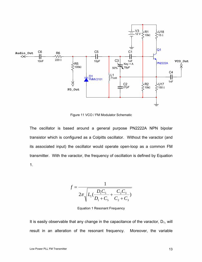
The output of the VCO* is fed back to a 74HC4040 high speed 12-stage binary
counter, which acts as a frequency divider. The PLL feedback loop schematic is
shown in Figure 12.
Figure 12 PLL Feedback Loop Schematic (Frequency Divider, Phase Detector & Loop Filter
By selecting output Q8 of the counter, the input FM signal is effectively divided by
512. Since the original signal is on the order of 100 MHz, the quotient is on the
*Actually, the output is from the RF amplifier, because the VCO signal output has a magnitude too low to trigger the clock of the counter IC. However, the premise is the same.
Low Power PLL FM Transmitter 14
order of 200 kHz – the proximity of the reference signal implemented by the
crystal oscillator circuitry.
2.2.4 Phase Detector
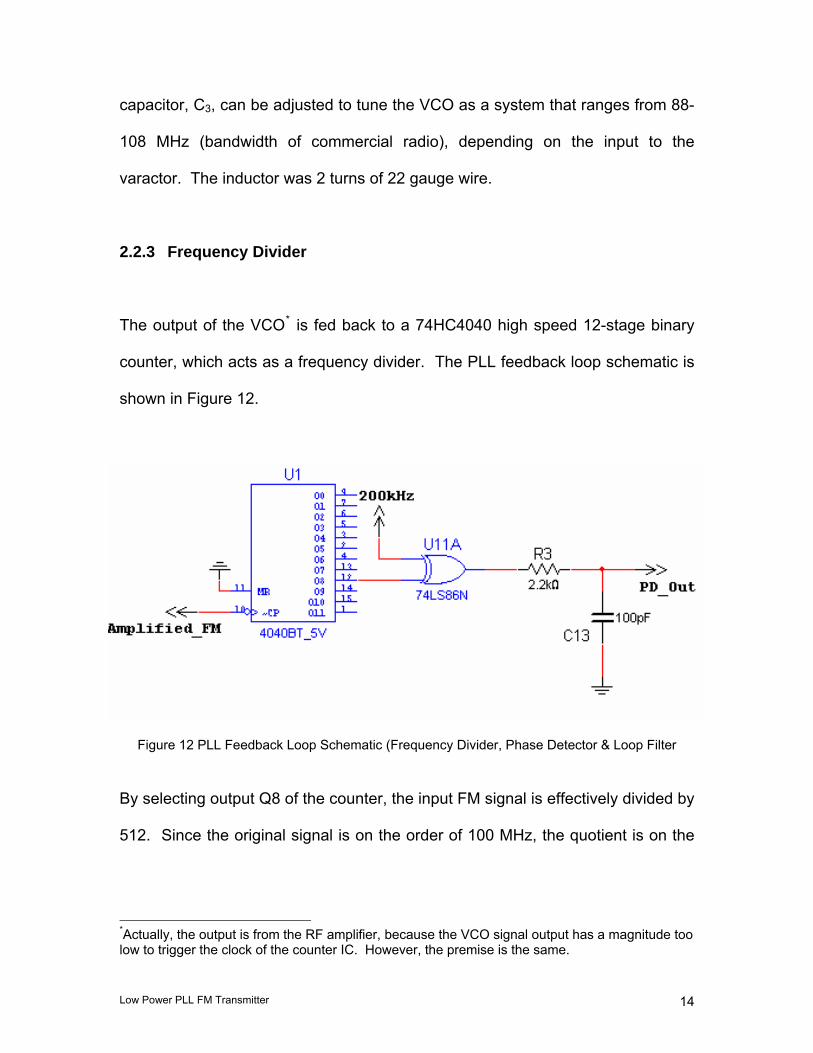
The purpose of the phase detector is to quantify the difference in frequency
and/or phase of any two input signals. In this case, a simple exclusive OR gate
[9], U11A (74LS86) in Figure 12, was utilized to generate the error signal.
As shown in Figure 13, the yellow square
wave represents the frequency-divided
version of the FM signal, the cyan square
wave represents the divided crystal
oscillation and the magenta waveform is the
error signal generated by the phase
detector. Figure 13 Phase Detector & Loop Filter Waveforms
This error signal is a variable-duty square wave that is based on the diversity of
the two inputs.
Low Power PLL FM Transmitter 15

2.2.5 Loop Filter
The structure of the loop filter is equivalent to that of a first order low-pass filter.
However, its purpose is actually to average (i.e. smooth) the error signal
generated by the phase detector, shown as the green waveform in Figure 13.
The cutoff frequency is chosen at an arbitrary multiple of the
operating frequency of the phase detector to ensure its proper
operation (in this case 723 kHz). The averaging causes the
capacitor to charge or discharge, as necessary, against the
varactor to adjust the VCO. This process continues until the
error signal has a zero duty cycle and the VCO is effectively
“locked” to the frequency of the crystal-based oscillator.
The physical layout of the PLL feedback loop is shown in Figure
14.
Figure 14 PLL Feedback Loop Layout
Low Power PLL FM Transmitter 16
2.3
2.3.1
FM Transmitter Module
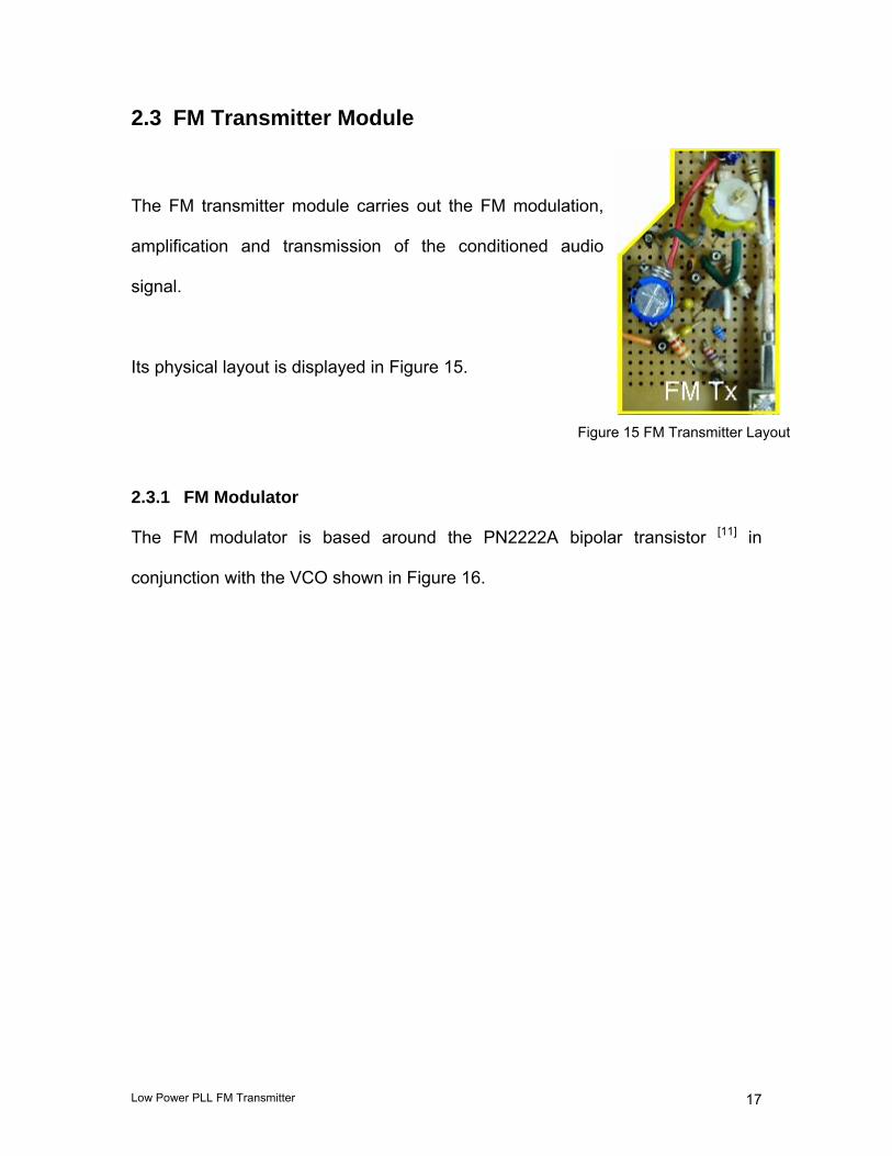
The FM transmitter module carries out the FM modulation,
amplification and transmission of the conditioned audio
signal.
Its physical layout is displayed in Figure 15.
Figure 15 FM Transmitter Layout
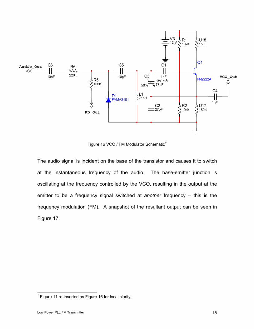
FM Modulator
The FM modulator is based around the PN2222A bipolar transistor [11] in
conjunction with the VCO shown in Figure 16.
Low Power PLL FM Transmitter 17
R110kΩ
R210kΩ
C1
1nF
C227pF
L171nH
V312 V
C4
1nF
C5
10pF R5100kΩ
D1FMMV2101
PD_Out
R6
220 Ω
C6
10nF VCO_Out
Audio_Out
U17150 Ω
U1815 Ω
C3Key = A 78pF 50%
Q1
PN2222A
Figure 16 VCO / FM Modulator Schematic†
The audio signal is incident on the base of the transistor and causes it to switch
at the instantaneous frequency of the audio. The base-emitter junction is
oscillating at the frequency controlled by the VCO, resulting in the output at the
emitter to be a frequency signal switched at another frequency – this is the
frequency modulation (FM). A snapshot of the resultant output can be seen in
Figure 17.
† Figure 11 re-inserted as Figure 16 for local clarity.
Low Power PLL FM Transmitter 18
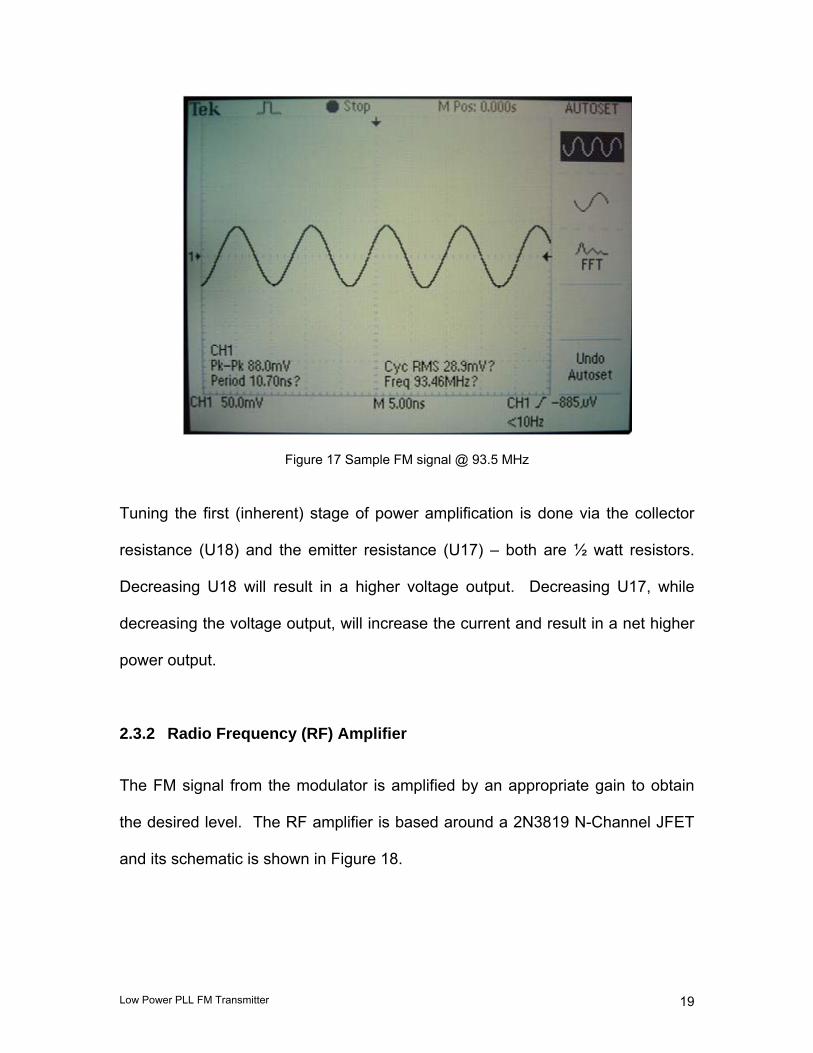
Figure 17 Sample FM signal @ 93.5 MHz
Tuning the first (inherent) stage of power amplification is done via the collector
resistance (U18) and the emitter resistance (U17) – both are ½ watt resistors.
Decreasing U18 will result in a higher voltage output. Decreasing U17, while
decreasing the voltage output, will increase the current and result in a net higher
power output.
2.3.2 Radio Frequency (RF) Amplifier
The FM signal from the modulator is amplified by an appropriate gain to obtain
the desired level. The RF amplifier is based around a 2N3819 N-Channel JFET
and its schematic is shown in Figure 18.
Low Power PLL FM Transmitter 19
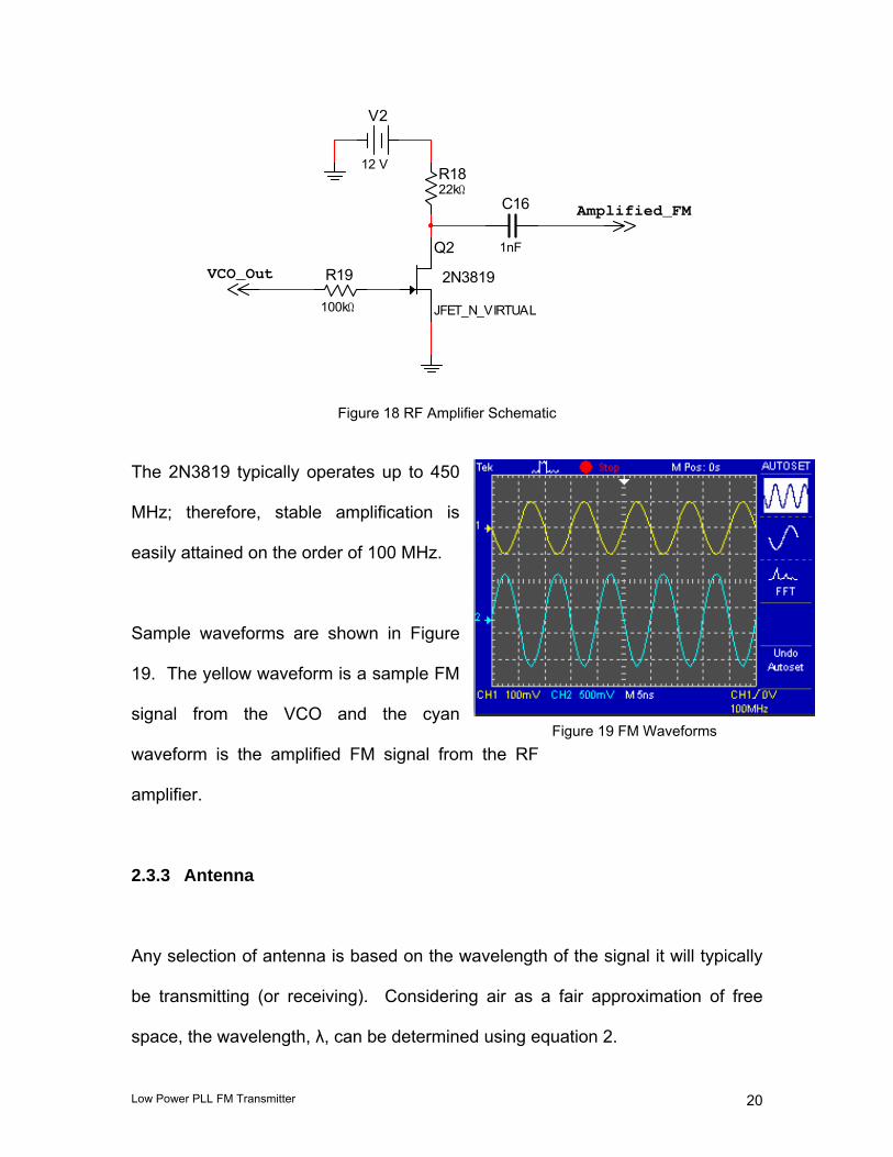
Q2
JFET_N_VIRTUAL
R1822kΩ
R19
100kΩ
V2
12 V
C16
1nF
Amplified_FM
VCO_Out 2N3819
Figure 18 RF Amplifier Schematic
The 2N3819 typically operates up to 450
MHz; therefore, stable amplification is
easily attained on the order of 100 MHz.
Sample waveforms are shown in Figure
19. The yellow waveform is a sample FM
signal from the VCO and the cyan
waveform is the amplified FM signal from the RF
amplifier.
Figure 19 FM Waveforms
2.3.3 Antenna
Any selection of antenna is based on the wavelength of the signal it will typically
be transmitting (or receiving). Considering air as a fair approximation of free
space, the wavelength, λ, can be determined using equation 2.
Low Power PLL FM Transmitter 20
fc
=λ
Equation 2 Wavelength Calculation
Where,
• c is the speed of light in a vacuum ≡ 3x10⁸m/s.
• f is the frequency of the signal – on the order of 100 MHz.
Using these values yields a wavelength of 3m.
This would be the ideal wavelength to utilize when calculating the length of
antenna to transmit the signal. However, when dealing with broadcasting, the
mechanical length becomes slightly less important (the importance of length
being predominant in directional transmissions). Therefore, the availability of a
2.4 GHz wireless router antenna was proposed as the LPPFMTx antenna.
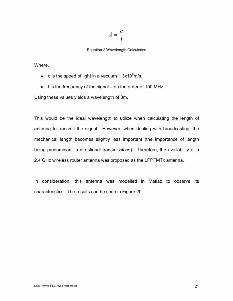
In consideration, this antenna was modelled in Matlab to observe its
characteristics. The results can be seen in Figure 20.
Low Power PLL FM Transmitter 21
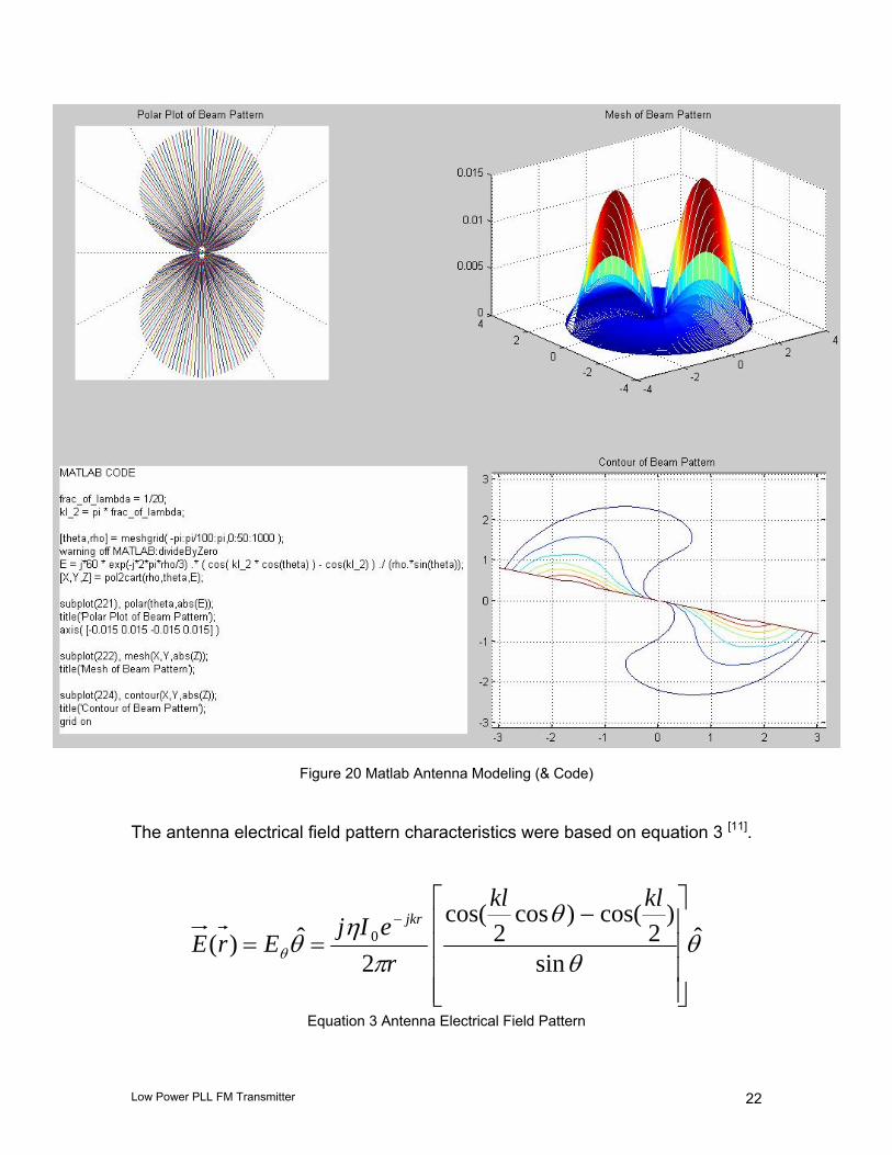
Figure 20 Matlab Antenna Modeling (& Code)
The antenna electrical field pattern characteristics were based on equation 3 [11].
θθ
θ
πη
θθ ˆsin
)2
cos()cos2
cos(
2ˆ)( 0
⎥⎥⎥⎥
⎦
⎤
⎢⎢⎢⎢
⎣
⎡ −==
−klkl
reIj
ErEjkr
Equation 3 Antenna Electrical Field Pattern
Low Power PLL FM Transmitter 22
It can be observed from the antenna characteristic plots that this antenna is
suitable for broadcast on the order of 100 MHz (as a λ/20 monopole) despite
being designed for 2.4 GHz. Moreover, its compact size is more desirable than
an antenna on the order of metres.
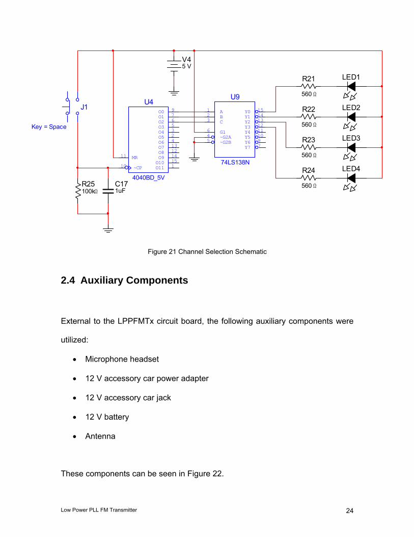
2.3.4 Channel Selection
The template for channel selection is set up such that, by pushing a normally-
open button, the channel will cycle between four pre-determined values.
Moreover, an LED will indicate the active channel.
The setup involves the de-bounced button to act as a clock input to the counter
which will address a 74LS138 decoder/demultiplexer. The active-low outputs of
the decoder will determine which channel is active. This is illustrated in Figure
21.
Low Power PLL FM Transmitter 23
U4
4040BD_5V
O10 15
O1 7
O11 1
O0 9
MR11
~CP10
O4 3O5 2O6 4O7 13O8 12O9 14
O2 6O3 5
U9
74LS138N
Y0 15Y1 14Y2 13Y3 12Y4 11Y5 10Y6 9Y7 7
A1B2C3
G16~G2A4~G2B5
J1
Key = Space
LED1
LED2
LED3
LED4
R21
560 Ω
R25100kΩ
C171uF
V45 V
R22
560 Ω
R23
560 Ω
R24
560 Ω
Figure 21 Channel Selection Schematic
2.4 Auxiliary Components
External to the LPPFMTx circuit board, the following auxiliary components were
utilized:
• Microphone headset
• 12 V accessory car power adapter
• 12 V accessory car jack
• 12 V battery
• Antenna
These components can be seen in Figure 22.
Low Power PLL FM Transmitter 24
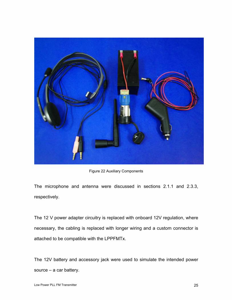
Figure 22 Auxiliary Components
The microphone and antenna were discussed in sections 2.1.1 and 2.3.3,
respectively.
The 12 V power adapter circuitry is replaced with onboard 12V regulation, where
necessary, the cabling is replaced with longer wiring and a custom connector is
attached to be compatible with the LPPFMTx.
The 12V battery and accessory jack were used to simulate the intended power
source – a car battery.
Low Power PLL FM Transmitter 25
3 RESULTS AND RECOMMENDATIONS
3.1 Performance Results
The audio module produces a noise-free voice signal that was tested for clarity
on quality-controlled speakers.
The FM output signal produced by the modulator in conjunction with the PLL
implementation is highly stable and carrying clean audio. Moreover, the system
possesses the tuneability of a common FM transmitter while maintaining crystal
stability.
The second stage RF amplifier allows for the adjustment of gain, such that the
desired broadcast radius can be achieved.
FM is broadcast at 115 mW – within the desired spec, such that it does not
impinge on government broadcast limitation laws (<1W). Current consumption is
84 mA – most of which can undoubtedly be attributed to the 7805 voltage
regulator.
Low Power PLL FM Transmitter 26
3.2
3.2.1
3.2.2
Problems / Implementation Issues
Microphone Biasing
Implementing the correct biasing network to extract audio from the microphone
was a preliminary issue. Slow iteration revealed the proper bias point without
damaging the internal crystal.
Immeasurable Inductance
Measuring the inductance of custom wound inductors proved non-trivial. After
successive iterations of unwinding, without actual reduction in inductance yielded
the discovery that the in-house LCR meter could not measure below an order of
μH (the inductance of the cabling was about 1.5 μH), while the orders of the
inductors in question were nH. As the highest quality piece of equipment, the
Tektronix oscilloscope was the basis of the design of a custom inductance (or,
more generally, reactance) meter. The design is shown in Figure 23.
Low Power PLL FM Transmitter 27
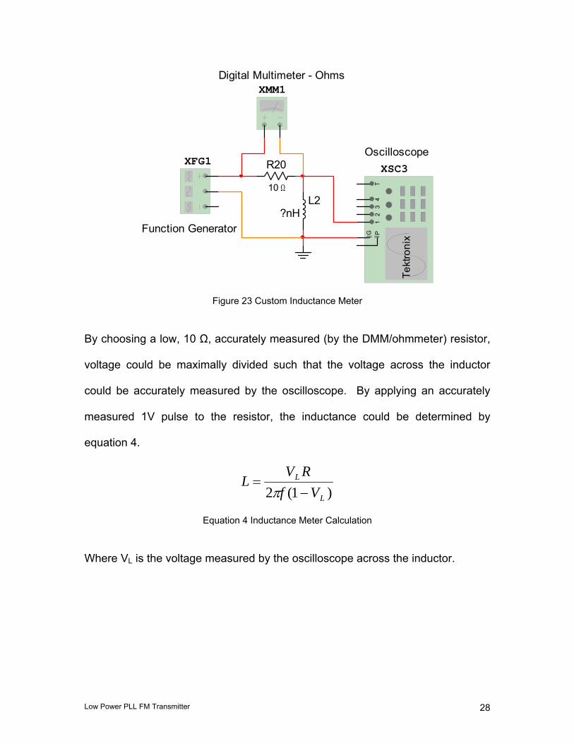
XFG1 R20
10 Ω L2
XSC3
Tekt
roni
x
12
34
TG P
XMM1
Function Generator
Digital Multimeter - Ohms
Oscilloscope
?nH
Figure 23 Custom Inductance Meter
By choosing a low, 10 Ω, accurately measured (by the DMM/ohmmeter) resistor,
voltage could be maximally divided such that the voltage across the inductor
could be accurately measured by the oscilloscope. By applying an accurately
measured 1V pulse to the resistor, the inductance could be determined by
equation 4.
)1(2 L
L
VfRV
L−
=π
Equation 4 Inductance Meter Calculation
Where VL is the voltage measured by the oscilloscope across the inductor.
Low Power PLL FM Transmitter 28
3.2.3
3.2.4
Frequency Division
The frequency divider (one of the main PLL components) first introduced
difficulties whereby the ICs chosen to perform the task were unable to function at
a frequency on the order of 100 MHz. Various implementations of 74LS series
frequency dividers, counters, flip flops and timers failed. The solution to the clock
frequency issue was resolved with the special order of the 74HC series (high
speed) 12 stage binary counter.
However, further issue arose due to the fact that the output FM signal from the
VCO had a magnitude too low to trigger the counter as an edge of the clock
(requiring a minimum of 2.4 V). This was resolved with the implementation of the
RF amplifier, which was necessary regardless.
RF Infection
Due to a freak accident while changing batteries, a current spike, which caused
the fuse to be blown, entered the LPPFMTx board. At best, some of the power
rail filtration was damaged causing the power rail and/or ground plane to be
infected with RF energy (due to acting as a receiving antenna of the FM
transmission).
Due to the fact that the ground plane was at a potential of 100 mV and oscillating
at a frequency on the order of 100 MHz, the audio conditioning could no longer
Low Power PLL FM Transmitter 29
function properly. This was a result of the fact that the output of the microphone,
before conditioning, is on the order of 5-10 mV. Therefore, when referenced to a
100 mV, 100 MHz ground plane, resulted in a lack of any remaining coherent
signal to be transmitted.
However, the FM transmitter module remained functional and could continue to
transmit, for example, tones from a function generator input directly to the base of
the first stage transistor.
Unfortunately, this issue could not be resolved before the project demo and will
remain unresolved until after graduation.
3.2.5 Recommended Design Improvements
To reduce the amount of RF infection within the circuit, the following methods
could be employed:
• Optocouplers/isolators – by optically isolating the RF and low frequency
(LF) portions of the circuit board, physical ground continuity can be
avoided and therefore, ground infection would not pose a problem to the
LF circuitry.
• PCB board development – by developing the LPPFMTx circuit on a printed
circuit board, RF infection can be reduced due to the shorter traces
required to connect circuit components. Moreover, microstrips allow for a
Low Power PLL FM Transmitter 30
more versatile matching network development between amplifiers, the
input (LF circuitry) and output (antenna).
• Toroidal cabling could be implemented at any transition between LF and
RF circuitry. This will confine any electric fields to within the toroid and
prevent and infection or leakage to other parts of the circuit.
To properly manage selecting between broadcast channels, one of the following
methods may be employed:
• Continuous Inductor Deformation – by attaching a deformable inductor to a
rotary knob, the resonance of the FM modulator can be adjusted. This
happens because the length of the inductor changes which causes the
inductance to change according to the relationship described in equation 5.
zdNdHL
4018)(
22
+=μ
Equation 5 Wheeler's Inductance Equation [12]
Where, d is the diameter, z is the length (both in inches) and N is the
number of turns.
• Discrete PWM/Varactor – by applying a PWM (possibly from a
microcontroller) to a varactor operating within the tuning paramaters of the
FM modulator, one can utilize its voltage-controlled capacitance to adjust
the resonance of oscillation, by varying the PWM duty cycle. Moreover,
Low Power PLL FM Transmitter 31

the existence of a microcontroller lends itself to the possible inclusion of
an LCD display that can display parameters such as the current broadcast
station.
Low Power PLL FM Transmitter 32
4 RESOURCES COST ANALYSIS
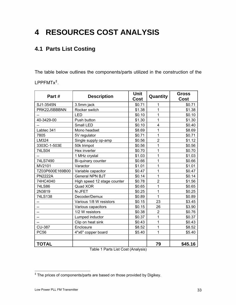
4.1 Parts List Costing
The table below outlines the components/parts utilized in the construction of the
LPPFMTx‡.
Part # Description Unit Cost Quantity Gross
Cost SJ1-3545N 3.5mm jack $0.71 1 $0.71PRK22J5BBBNN Rocker switch $1.38 1 $1.38-- LED $0.10 1 $0.1040-3429-00 Push button $1.30 1 $1.30-- Small LED $0.10 4 $0.40Labtec 341 Mono headset $8.69 1 $8.697805 5V regulator $0.71 1 $0.71LM324 Single supply op-amp $0.56 2 $1.123303C-1-503E 50k trimpot $0.56 1 $0.5674LS04 Hex inverter $0.70 1 $0.70-- 1 MHz crystal $1.03 1 $1.0374LS7490 Bi-quinary counter $0.66 1 $0.66MV2101 Varactor $1.01 1 $1.01TZ03P600E169B00 Variable capacitor $0.47 1 $0.47PN2222A General NPN BJT $0.14 1 $0.1474HC4040 High speed 12 stage counter $0.78 2 $1.5674LS86 Quad XOR $0.65 1 $0.652N3819 N-JFET $0.25 1 $0.2574LS138 Decoder/Demux $0.89 1 $0.89-- Various 1/8 W resistors $0.15 23 $3.45-- Various capacitors $0.15 26 $3.90-- 1/2 W resistors $0.38 2 $0.76-- Lumped inductor $0.37 1 $0.37-- Clip on heat sink $0.43 1 $0.43CU-387 Enclosure $8.52 1 $8.52PC56 4"x6" copper board $5.40 1 $5.40
TOTAL 79 $45.16Table 1 Parts List Cost (Analysis)
‡ The prices of components/parts are based on those provided by Digikey.
Low Power PLL FM Transmitter 33
The designed distance of the LPPFMTx is on the order of 1 km (about 3281 feet),
according to Amazon.com, the range of prices for a PLL FM transmitter that has
a range of 10-30 feet is about $25-60 USD (about $30-70 CAD) and for 150-300
feet, the cost is about $90-160 USD (about $105-185 CAD) [13].
This illustrates the marketability and competitive nature of the LPPFMTx design
as a commercial product.
4.2 Equipment and Software
The following lab equipment and commercial software were utilized in the design,
testing and debugging of the LPPFMTx.
Lab Equipment
• Breadboard
• Oscilloscope
• Function generator
• DC power supply
• Digital multimeter
• LCR meter
• 12 V lead acid battery
Software
• Microchip Technology Inc FilterLab
• Orcad PSpice
• Electronic Workbench Multisim
• Mathworks Matlab
• Microsoft Excel
Low Power PLL FM Transmitter 34
5 REFERENCES
[1]. Untitled, Undated. Retrieved on July 24, 2006 from <http://www.vinland.ca/header.htm>.
[2]. Wikipedia (2006). Autocross. Wikipedia. Retrieved on July 24, 2006 from
<http://en.wikipedia.org/wiki/Autocross>.
[3]. Browne, Greg (2006). Low Power PLL-Based FM Transmitter.
[4]. Labtec Mono 341 PC Headset Microphone SKYPE/VOIP/GAMING (Undated). Retrieved
on January 29, 2007 from <http://stores.ebay.ca/Reforger>.
[5]. Engdahl, T (1997). Powering Microphone. Retrieved on February 7, 2007 from
<http://www.epanorama.net/circuits/microphone_powering.html>.
[6]. Hearing (sense). (2007). In Wikipedia, The Free Encyclopedia. Retrieved on January 29,
2007, from
<http://en.wikipedia.org/w/index.php?title=Hearing_%28sense%29&oldid=118544964>.
[7]. Wikipedia (2006). Phase-locked loop. Wikipedia. Retrieved on July 26, 2006 from
<http://en.wikipedia.org/wiki/PLL>.
[8]. Scherrer, T (2007). Crystal Oscillator Circuits. Retrieved on March 15, 2007, from
<http://www.z80.info/uexosc.htm>.
[9]. Van Roon, T (2001). Phase-Locked Loop Tutorial, PLL. Retrieved on February 2, 2007,
from <http://www.uoguelph.ca/~antoon/gadgets/pll/pll.html>.
[10]. Incepinar, B (2001). Simple 20 Meters Range FM Transmitter. Retrieved on February
16, 2007 from <http://tacashi.tripod.com/elctrncs/smplfmtr/smplfmtr.htm>.
[11]. Gill, E. (2005). Thin, Linear Wire Antennas (Equation 3.8). St. John’s: Memorial
University of Newfoundland.
[12]. RF Café (2007). Inductors & Inductance Calculations Formulas Equations. Retrieved on
February 26, 2007, from <http://www.rfcafe.com/references/electrical/inductance.htm>.
Low Power PLL FM Transmitter 35

[13]. Google (2007). Search for PLL FM transmitters on Amazon.com. Retrieved on April 3,
2007 from <http://www.google.ca/search?q=pll+fm+transmitter+-review+-inurl:page+-
inurl:search+site:www.amazon.com&hl=en&rls=GGGL,GGGL:2006-31,GGGL:en&filter=0>.
Low Power PLL FM Transmitter 36
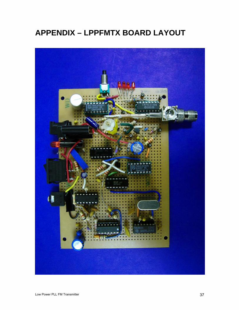
APPENDIX – LPPFMTX BOARD LAYOUT
Low Power PLL FM Transmitter 37