LOW POWER DESIGN OF 8B/10B ENCODER AND …eprints.usm.my/39575/1/ONG_JI_XIAN_24_Pages.pdf ·...
37
LOW POWER DESIGN OF 8B/10B ENCODER AND 10B/8B DECODER USING CLOCK GATING TECHNIQUE by ONG JI XIAN A Dissertation submitted for partial fulfilment of the requirement for the degree of Master of Science (Microelectronic Engineering) August 2017
Transcript of LOW POWER DESIGN OF 8B/10B ENCODER AND …eprints.usm.my/39575/1/ONG_JI_XIAN_24_Pages.pdf ·...
LOW POWER DESIGN OF 8B/10B
ENCODER AND 10B/8B DECODER USING CLOCK GATING
TECHNIQUE
by
ONG JI XIAN
A Dissertation submitted for partial fulfilment of the requirement for
the degree of Master of Science (Microelectronic Engineering)
August 2017

i
ACKNOWLEDGEMENT
First of all, thanks to Intel and my managers for the supporting and providing
the fund for me to complete my research. Second, I would like to take this opportunity
to express my appreciation to my supervisor, Dr. Nor Muzlifah Mahyuddin. Appreciate
her guidance throughout the entire project. Third, thanks to my both examiners, Ir. Dr.
Nor Asiah and Dr. Mohamed Fauzi. Thanks for their comment and make this
dissertation more valuable. Lastly, thanks to my friends who directly or indirectly help
me to complete the project.

ii
TABLE OF CONTENTS
ACKNOWLEDGEMENT .......................................................................................................... i
TABLE OF CONTENTS ........................................................................................................... ii
LIST OF TABLES ............................................................................................................... vi
LIST OF FIGURES .............................................................................................................. vii
LIST OF ABBREVIATIONS ................................................................................................... ix
ABSTRAK ............................................................................................................... xi
ABSTRACT .............................................................................................................. xii
CHAPTER 1 INTRODUCTION .................................................................................. 1
1.1 Background ...................................................................................................... 1
1.2 Problem Statements .......................................................................................... 2
1.3 Objective .......................................................................................................... 3
1.4 Research Scope ................................................................................................. 4
1.5 Thesis Outline ................................................................................................... 4
CHAPTER 2 LITERATURE REVIEW ....................................................................... 6
2.1 Introduction ...................................................................................................... 6
2.2 Performance Metrics ........................................................................................ 6
2.3 Comparison of Line Codes ............................................................................... 8
2.4 8B/10B Encoder and 10B/8B Decoder .......................................................... 10
2.4.1 Operation of 8B/10B Encoder ................................................................ 10
iii
2.4.2 Special Character .................................................................................... 14
2.4.3 Operation of 10B/8B Decoder ................................................................ 15
2.5 Power Reduction Techniques ......................................................................... 19
2.5.1 Multi Voltage Source .............................................................................. 20
2.5.2 Power Gating .......................................................................................... 21
2.5.3 Clock Gating ........................................................................................... 22
2.6 Summary ........................................................................................................ 23
CHAPTER 3 METHODOLOGY ............................................................................... 25
3.1 Introduction .................................................................................................... 25
3.2 Logical Implementation of 8B/10B Encoder and 10B/8B Decoder ............... 27
3.2.1 Logical Implementation of 8B/10B Encoder .......................................... 27
3.2.1.1 Data Path Design of 5B/6B Encoder .................................................. 28
3.2.1.2 Data Path Design of 3B/4B Encoder .................................................. 32
3.2.1.3 Disparity Control Unit Design of 8B/10B Encoder ........................... 34
3.2.2 Logical Implementation of 10B/8B Decoder ......................................... 38
3.2.2.1 Data Path Design of 6B/5B Decoder.................................................. 38
3.2.2.2 Data Path Design of 4B/3B Decoder.................................................. 42
3.3 Behavioral Implementation of 8B/10B Encoder and 10B/8B Decoder ......... 45
3.3.1 Behavioral Implementation of 8B/10B Encoder..................................... 45
3.3.1.1 Data Path Design of 5B/6B Encoder .................................................. 46
3.3.1.2 Data Path Design of 3B/4B Encoder .................................................. 47
iv
3.3.1.3 Disparity Control Unit of 8B/10B Encoder........................................ 48
3.3.2 Behavioral Implementation of 10B/8B Decoder .................................... 50
3.4 Clock Gating Design Implementation and Power Analysis ........................... 50
3.5 Summary ........................................................................................................ 51
CHAPTER 4 RESULTS AND DISCUSSION ........................................................... 53
4.1 Introduction .................................................................................................... 53
4.2 Simulation Results for Logic Implementation of 8B/10B Encoder and 10B/8B
Decoder .......................................................................................................... 53
4.2.1 Simulation Results of 8B/10B Encoder .................................................. 54
4.2.2 Simulation Results of 8B/10B Decoder .................................................. 59
4.3 Simulation Results of Behavioral Implementation 8B/10B Encoder and
10B/8B Decoder ............................................................................................. 61
4.3.1 Simulation Results of 8B/10B Encoder .................................................. 62
4.3.2 Simulation Results of 10B/8B Decoder .................................................. 67
4.4 Clock Gating Design and Clock Gating Implemented Encoder/Decoder ...... 71
4.5 Power Analysis of Behavioral Implementation 8B/10B Encoder and 10B/8B
Decoder .......................................................................................................... 77
4.6 Summary ........................................................................................................ 78
CHAPTER 5 CONCLUSIONS AND FUTURE WORK ........................................... 80
5.1 Conclusion ...................................................................................................... 80
5.2 Future Work ................................................................................................... 81
v
References .............................................................................................................. 82
APPENDIX A CLOCK GATING CIRCUIT VERILOG HDL CODES ...................... A-1
APPENDIX B LOGIC IMPLEMENTATION CIRCUIT VERILOG HDL CODES ... B-1
APPENDIX C BEHAVIORAL IMPLEMENTATION CIRCUIT VERILOG HDL
CODES ................................................................................................. C-1
vi
LIST OF TABLES
Table 2.1 Type of Codes with DSV Parameters ........................................................... 9
Table 2.2 5B/6B Encoding Table ................................................................................ 12
Table 2.3 3B/4B Encoding Table ................................................................................ 14
Table 2.4 Encoding Table for Special Character ........................................................ 15
Table 2.5 6B/5B Decoding Table ............................................................................... 16
Table 2.6 4B/3B Decoding Table ............................................................................... 18
Table 3.1 Truth Table of Classifications circuit .......................................................... 29
Table 3.2 Input Classifications of 5B/6B Encoder ...................................................... 30
Table 3.3 Input Classifications of 3B/4B Encoder ...................................................... 32
Table 3.4 Disparity Classifications of 5B/6B Encoder ................................................ 34
Table 3.5 Disparity Classifications of 3B/4B Encoder ................................................ 36
Table 3.6 Input Classifications of 6B/5B Decoder ...................................................... 39
Table 3.7 Input Classifications of 4B/3B Decoder ...................................................... 43
Table 3.8 Output Mapping of Behavioral Implementation 5B/6B Encoder ................ 46
Table 3.9 Output Mapping of Behavioral Implementation 3B/4B Encoder ................ 47
Table 4.1 Simulated Power of 8B/10B Encoder by Xilinx XPower Analysis ............. 77
Table 4.2 Simulated Power of 10B/8B Decoder by Xilinx XPower Analysis ............ 78
vii
LIST OF FIGURES
Figure 2.1 The Output comparison between NRZ(M), Miller and Manchester. ........... 9
Figure 2.2 The Block Diagram of an 8B/10B Encoder .............................................. 11
Figure 2.3 Data arrangements in encoding process .................................................... 12
Figure 2.4 (a) AND Gate Clock Gating (b) Latch Based Clock Gating (c) Flip-flop
Based Clock Gating ................................................................................... 22
Figure 3.1 Design Process Flow .................................................................................. 26
Figure 3.2 8B/10B Encoder Structure Organization .................................................... 28
Figure 3.3 10B/8B Decoder Organization ................................................................... 38
Figure 3.4 FSM of Disparity Control Unit................................................................... 49
Figure 3.5 Clock Gate Cell .......................................................................................... 51
Figure 4.1 Simple block diagram of 8B/10B Encoder Structure ................................. 54
Figure 4.2 Simulation Waveform for Logic Implementation 8B/10B Encoder from 0 ps
.................................................................................................................... 55
Figure 4.3 Simulation Result at Lower Four Bits Output, fghj = 100 ......................... 58
Figure 4.4 Simulation Waveform for Logical Implementation 10B/8B Decoder from 0
ps. ............................................................................................................... 60
Figure 4.5 Simulation Waveform for Behavioral Implementation 8B/10B Encoder from
0 ps. ............................................................................................................ 63
Figure 4.6 Simulation Result at Lower Four Bits Output, fghj = 1000. ...................... 65
Figure 4.7 State Machine Sequence of 5B/6B Encoder ............................................... 66
viii
Figure 4.8 Simulation Waveform for Behavioral Implementation 10B/8B Decoder from
0 ps. ............................................................................................................ 68
Figure 4.9 Simulation Waveform When Decoding Lower Four Bits Encoded Data, fghj
= 0101. ....................................................................................................... 70
Figure 4.10 Coding Sequence for Clock Gating Cell without Temporary Buffer ....... 72
Figure 4.11 Coding Sequence for Clock Gating Cell with Temporary Buffer, clk_en 72
Figure 4.12 The Waveform of Gated Clock Signal ..................................................... 73
Figure 4.13 Simulation Waveform of Logical Implementation 8B/10B Encoder and
10B/8B Decoder with Clock Gating .......................................................... 75
Figure 4.14 Simulation Waveform of Behavioral Implementation 8B/10B Encoder and
10B/8B Decoder with Clock Gating .......................................................... 76

ix
LIST OF ABBREVIATIONS
Abbreviation Meaning
4B/5B 4 Bits to 5 Bits
4B/3T 4 Bits to 3 Ternary
64B/66B 64 Bits to 66 Bits
6B/8B 6 Bits to 8 Bits
8B/10B 8 Bits to 10 Bits
8B/6T 8 Bits to 6 Ternary
B Bit(s)
CRC Cyclic redundancy check
D0 Running disparity of the current encoded output
D-1 Running disparity of the before encoded output
FSM Finite state machine
HDL Hardware Description Language
HDMI High-Definition Multimedia Interface
IP Intellectual Property
LSB Least significant bit
MSB Most significant bit
NRZ Non-Return-Zero
NRZ(M) Non-return-to-zero mark
RD Running disparity
RL Run length
RZ Return-Zero
SATA Serial ATA

x
USB Universal Serial Bus

xi
REKA BENTUK 8B/10B ENGEKOD DAN 10B/8B PENYAHKOD BERKUASA
RENDAH DENGAN TEKNIK PENGEGATAN JAM
ABSTRAK
8B/10B Pengekod dan 10B/8B Penyahkod boleh dijumpai di dalam kebanyakkan
aplikasi elektronik dengan penghantaran tinggi, contohnya, ATA berangkai (SATA), USB3.0
dan applikasi fiber optikal. Disebabkan oleh keseimbangan arus terus (AT), ia tidak
memerlukan lebih daripada lima bits berterusan untuk menghasilkan pemulihan jam yang
berkesan dan pengesanan ralat yang mudah pada data yang telah dikodkan. Dengan populasi
peranti mudah alih dalam pasaran, rekabentuk dengan kuasa rendah menjadi salah satu
kekangan yang sangat penting dalam reka bentuk litar elektronik. Oleh kerana 8B/10B
Pengekod akan digunakan dalam komponen pengalihan data dengan kelajuan tinggi, pereka
bentuk yang berkuasa rendah amat diperlukan di pasaran elektronik. Di dalam projek ini, dua
perlaksanaan bagi 8B/10B pengekod/penyahkod direkabentuk dan dilaksanakan bersama litar
pengegetan jam. Di dalam pelaksannan logikal, semua hasil dari litar akan direka dalam bentuk
lojik boolean, tetapi di dalam pelaksanaan berdasarkan tingkahlaku, litar direkabentuk dengan
mengunakan ciri-ciri pengekod/penyahkod sahaja tanpa mengenal pasti litar lojik pengekod
tersebut. Semua litar akan direkabentuk dengan menggunakan Verilog HDL dan disimulasikan
dengan ModelSim. Analisis kuasa akan dijalankan untuk membandingkan prestasi kuasa bagi
litar bersama pengegetan jam dan litar sebelum pengegetan jam. Analisis kuasa akan dijalankan
untuk frekuensi 20 MHz dan 200 MHz dengan bantuan Xilinx Power Analysis Tool. Dengan
20 MHz frekuensi, kuasa hierarki pengekod yang telah bersama pengegatan telah dikurangkan
dengan 38.24 % dan 8.33 % kuasa hierarki dikurangkan dalam penyahkod. Dengan 200 MHz
frekuensi, kuasa hierarki telah dikurangkan daripada sebanyak 45.28 % dalam pengekod dan
8.47 % dalam penyahkod.
xii
LOW POWER DESIGN OF 8B/10B
ENCODER AND 10B/8B DECODER USING CLOCK GATING TECHNIQUE
ABSTRACT
8B/10B Encoder and 10B/8B Decoder can be found in most of the high transmission
speed electronic application such as Serial ATA (SATA), Universal Serial Bus (USB) 3.0 and
optical fiber applications. This is due to the DC balance, not more than five consecutive bits
which leads to reliable clock recovery and easiness of error detection of the encoded data. Due
to the market demand of portable devices, the low power design become one of the critical
design concern of electronic circuit. Since 8B/10B Encoder will be using in the high speed data
transferring components, low power design of the encoder will be needed by the market. In
this project two implementation of 8B/10B Encoder and 10B/8B Decoder are designed and
implement with clock gating circuit. The logical implementation method is designed from
finding the boolean logic of every output, while behavioral implementation method is designed
by only behavioral of the encoder/decoder. All the circuits were designed with Verilog
Hardware Description Language (HDL) and simulated with ModelSim. The clock gating
circuit is simple, easy to be implemented to the circuit and effectively reduce the clock activity,
eventually reduced the dynamic power of the circuit. The power analysis is done under 20 MHz
and 200 MHz clock frequencies with the help of Xilinx Power Analysis Tool. At 20 MHz,
38.24 % of the hierarchy power has been reduced for clock gated 8B/10B Encoder and 8.33 %
reduction for clock gated 10B/8B Decoder. At 200 MHz, 45.28 % of the hierarchy power has
been reduced for clock gated 8B/10B Encoder and 8.47 % reduction for clock gated 10B/8B
Decoder.
1
CHAPTER 1
INTRODUCTION
1.1 Background
Line coding is a very important data transferring technique used in digital
system. The idea of line coding is to ensure the data transferring by digital system with
high efficiency and high accuracy. The input data will be encoded by rearranging or
manipulating the input data according to the algorithm of the specific line coding
method.
The common line coding techniques used are Non-Return-Zero (NRZ), Polar
NRZ, Return-Zero (RZ) and etc. These techniques are further enhanced to 4 Bits to 5
Bits (4B/5B), 4 Bits to 3 Ternary (4B/3T), 6 Bits to 8 Bits (6B/8B), 8 Bits to 6 Ternary
(8B/6T), 8 Bits to 10 Bits (8B/10B), 64 Bits to 66 Bits (64B/66B) and etc. All of these
line codes are mainly to increase the performance of the data transferring as well as
data recovering. The data will be encoded in the transmitter in order to transfer the data
out to the receiver, and the decoder in receiver will decode the encoded data to the
original data. Therefore, it is very important to have a method that is able to transfer the
data in simple, fast and with easy of recovery.
Due to the evolution of the digital system and device, the complexity of the data
also increases. Thus a line coding technique that is able to process these complex data
in a faster and accurate way are demanded to implement into the device. The method
used in 8B/10B Encoder to encode the data input can ensure the data transfer faster and
easier recovery. This explains the ever increasing demand of 8B/10B Encoder
2
implementation. The 8B/10B Encoder can be easily found in the high data transfer rate
device such as USB 3.0, High-Definition Multimedia Interface (HDMI), SATA, and
optical fiber application [1].
1.2 Problem Statements
In the world of high speed communication system, there is also a need for a fast
data delivery and with bigger capacity. However with this comes a problem of baseline
offset and unbalance code flow [2]. In order to overcome this issue, the 8B/10B Encoder
is used as it has a very low percentage error in transmission and DC compensation
function to enhance the accuracy of the data transmission.
The 8B/10B Encoder and 10B/8B Decoder has a quite simple circuit
implementation but a very complicated logic implementation. Thus in order to simplify
the logic implementation of the 8B/10B Encoder and 10B/8B Decoder, an idea
proposed by [3] which adapts a lookup table mechanism in order to map the logic into
the structure of the encoder, simplifying the design process.
Nowadays, low power consumption is one of the important constraints in the
current trending of electronic design. This is due to the increase of demanding of the
portable devices such as mobile phone, laptop and tablets, they become part of the
lifestyle of most of the people and one of the limitation of the portable device are battery
life. Additionally, with other high speed device, the power consumption to drive the
speed of this will be significantly high. As the power itself is directly proportional to
the switching activity of the device, the faster the process is, the higher the power
consumption will be.
3
The most common power reduction technique is by reducing the voltage supply.
This may work effectively for dynamic power consumption but has little or no effect
on the static power consumption. Besides by reducing the voltage supply, it will
significantly reduce the driving current at the output of the device which insignificantly
reduce the speed of the data transmission. Moreover, by reducing the voltage supply,
the power consumption for the high speed device like 8B/10B Encoder will remain high
as the mechanism is heavily depending on the switching of the clock.
Another method that can reduce both dynamic and static power consumption,
as well as able to control the switching activity of the clock is known as clock gating.
In this technique, the clock is disabled at when it is unnecessary [4]. Thus, reducing the
power consumption without affecting overall performance.
Therefore, with simplified version of the logic implementation by using the
lookup table, the implementation of clock gating circuit into the encoder is significantly
easy. The effect of clock gating implementation on power consumption for both version
of 8B/10B Encoder and 10B/8B Decoder will be discussed later.
1.3 Objective
The objectives of this research are:
1. To develop an 8B/10B Encoder and 10B/8B Decoder using the
conventional logic implementation.
2. To develop an 8B/10B Encoder and 10B/8B Decoder without finding
the logical circuit of the decoder, i.e. behavioral implementation.

4
3. To reduce more than 50 % of the power consumption of the 8B/10B
Encoder and more than 0 % of the power consumption of the 10B/8B
Decoder by using simple latch based clock gating technique.
1.4 Research Scope
There are three scopes included in this research. First, design and investigate
the functional of the 8B/10B by using Verilog HDL and simulated it by using
ModelSim. Second, the power analysis of the designs are carried out with clock
frequencies of 20 MHz and 200 MHz by using Xilinx ISE suit. Clock gating cell is
designed and examine the impact of clock gating to the encoders and the decoders.
1.5 Thesis Outline
This dissertation is organized into four chapters. The rest of the dissertation is
organized as follow.
In Chapter 2, the first subtopic will be discussing about the idea, the objective
and the functionality of 8B/10B Encoder and 10B/8B Decoder. The discussion will be
followed by the power reduction techniques that had been or had not been implemented
in the 8B/10B Encoder and 10B/8B Decoder. The comparison of those researches will
be discussed at the end of this chapter.
In Chapter 3, the process of encoders and decoder will be discussed. The design
flow of logical implementation 8B/10B Encoder and 10B/8B Decoder, behavioral
implementation 8B/10B Encoder and clock gate will be shown in this chapter. The
intentions of every steps will be stated in this chapter as well.

5
The simulation result of the encoders and decoders will be discussed in Chapter
4. The result will be discussed with simulation waveform, and power estimation result
will be attached with the discussion.
The conclusion and the future work of the research will be concluded in Chapter
5.
6
CHAPTER 2
LITERATURE REVIEW
2.1 Introduction
Modern communications nowadays need a very high transmission speed, the
encoder is one of the important component to achieve this. The encoding techniques
used proposed for 8B/10B Encoder are very useful in high speed communication
system such as optical fiber applications, gigabit Ethernet and USB3.0 or higher [5, 6].
The easier of error detection, DC balancing and less power consumption are the
advantages provided by 8B/10B Encoder. This is due to the limitation of run length and
the balance code flow. In this chapter, the performance metrics will be discussed at first,
then followed by operation of 8B/10B Encoder and 10B/8B Encoder and lastly
comparison between various power reduction techniques.
2.2 Performance Metrics
There are several important parameter metrics of line coding such as digital sum
variation (DSV), disparity, run length and DC-balance. They are all directly impact
quality of the transmitted data. The definition of DSV is the sum of the running energy
between the maximum and the minimum value of the codes. In binary codes, the value
of 1’s is +1, while value of 0’s will be –1. This is used to measure the DC value in the
data stream [7, 8].
7
Run Length (RL) is the number of a continuous bits in the sequence [9]. For
example, in the sequence of 111100, the RL of 1’s at the beginning is four, then
followed by two RL of 0’s. This is very important factor for clock and data recovery
(CRD) [6, 7, 9–11], the longer the RL, the lower the reliability of the CRD. Running
disparity (RD) is another measurement for line code. RD is defined as the difference
between the numbers of 1’s and the number of 0’s in the group of data. The running
disparity can be calculate by the equation below [12]:
𝑅𝐷 = ∑ 1′𝑠 − ∑ 0′𝑠 (2.1)
Where,
RD is the running disparity,
∑ 1′𝑠 is the total numbers of bit 1 in the encoded data,
∑ 0′𝑠 is the total numbers of bit 0 in the encoded data.
If the RD is negative (-) which means the numbers of 1’s is less than the numbers
of 0’s in the encoded data; if RD is positive (+) which means the numbers of 1’s more
than the numbers of 0’s in the encoded data; if RD is neutral (0) which means both
numbers of 1’s and numbers of 0’s are equal. RD plays a very important role in the
8B/10B Encoder and 10B/8B Decoder, this will be discussed in the following section.
The RD is used to control the DC Balance of the encoded data. If the numbers
of 1’s and 0’s are balance in a series of encoded data, the data is DC-free or DC balance.
The unbalanced DC will caused the shifting the voltage level of the AC-coupled data
links of the device and cause error data in the receiver side. In a simple words, this is
avoid the DC component is sending through the transmission channel. As the channels
8
are rich with most of the AC components, such as capacitor and inductor, that will
caused the wrong data is received by the receiver. Therefore, a balance number of 1’s
and 0’s of the transmitting data can avoid the DC shifting[2, 9].
2.3 Comparison of Line Codes
Non-return-to-zero mark (NRZ(M)) is a simple line coding method. The output
data will be toggle when the input bit 1 is detected, and bit 0 will be remain unchanged
[13]. As a result, the line code do is not bounded the data, the output data will be having
a possible a long sequence of 1’s or 0’s. Therefore, it is DC unbalance coding. The DC
component will be sending through the transmission channel and hard to recovery the
data.
The operation of Miller is similar with NRZ(M) but in the Miller coding, if two
consecutive 0’s, the signal will be toggled [14]. Therefore, this coding method are able
to reduce the DC component of the output, but this method will still having DC
unbalance situation and clock recovery are not easy as 8B/10B encoding. Another
coding method called Manchester. The output data of this coding will be toggle as clock
when the input data is 1, and inverted the toggling signal of clock when the input data
is “0” [15]. This coding method is able to produce the DC balance coding method. But
since the output will be toggled as the same as the clock, high bandwidth is needed at
the receiver as compared to Miller coding and 8B/10B encoding.
The example outputs of these three different coding methods are shown in
Figure 2.1.
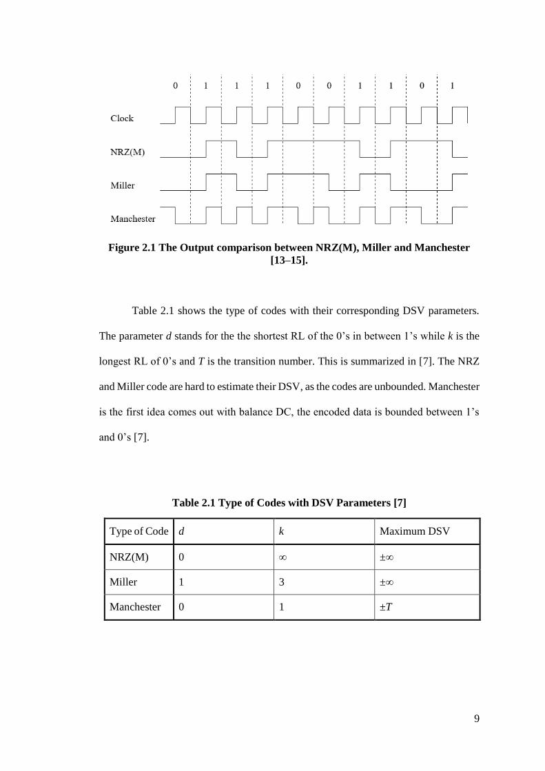
9
Figure 2.1 The Output comparison between NRZ(M), Miller and Manchester
[13–15].
Table 2.1 shows the type of codes with their corresponding DSV parameters.
The parameter d stands for the the shortest RL of the 0’s in between 1’s while k is the
longest RL of 0’s and T is the transition number. This is summarized in [7]. The NRZ
and Miller code are hard to estimate their DSV, as the codes are unbounded. Manchester
is the first idea comes out with balance DC, the encoded data is bounded between 1’s
and 0’s [7].
Table 2.1 Type of Codes with DSV Parameters [7]
Type of Code d k Maximum DSV
NRZ(M) 0 ∞ ±∞
Miller 1 3 ±∞
Manchester 0 1 ±T
10
2.4 8B/10B Encoder and 10B/8B Decoder
The first idea of 8B/10B was suggested by Albert X. Wider and Peter A.
Franaszek in 1983 [8]. The coding method is targeted to be DC balanced which means
the encoded data will have a balanced number of 1’s and 0’s and the run length of the
encoded data will be less than continuous of five 1’s or 0’s. Thus, the encoded will have
a good clock recovery and able to avoid the DC shifting [2, 8, 12, 16].
2.4.1 Operation of 8B/10B Encoder
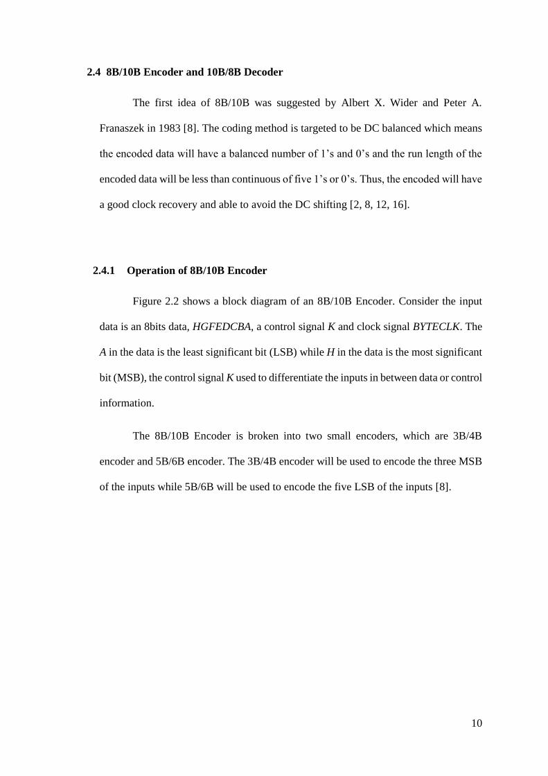
Figure 2.2 shows a block diagram of an 8B/10B Encoder. Consider the input
data is an 8bits data, HGFEDCBA, a control signal K and clock signal BYTECLK. The
A in the data is the least significant bit (LSB) while H in the data is the most significant
bit (MSB), the control signal K used to differentiate the inputs in between data or control
information.
The 8B/10B Encoder is broken into two small encoders, which are 3B/4B
encoder and 5B/6B encoder. The 3B/4B encoder will be used to encode the three MSB
of the inputs while 5B/6B will be used to encode the five LSB of the inputs [8].
11
Figure 2.2 The Block Diagram of an 8B/10B Encoder [8]
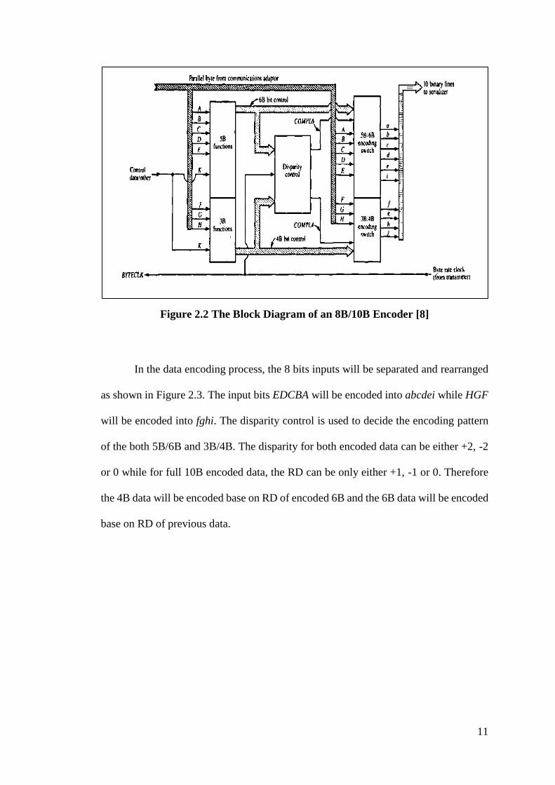
In the data encoding process, the 8 bits inputs will be separated and rearranged
as shown in Figure 2.3. The input bits EDCBA will be encoded into abcdei while HGF
will be encoded into fghi. The disparity control is used to decide the encoding pattern
of the both 5B/6B and 3B/4B. The disparity for both encoded data can be either +2, -2
or 0 while for full 10B encoded data, the RD can be only either +1, -1 or 0. Therefore
the 4B data will be encoded base on RD of encoded 6B and the 6B data will be encoded
base on RD of previous data.
12
Figure 2.3 Data arrangements in encoding process [17]
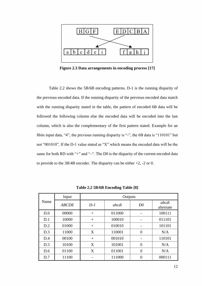
Table 2.2 shows the 5B/6B encoding patterns. D-1 is the running disparity of
the previous encoded data. If the running disparity of the previous encoded data match
with the running disparity stated in the table, the pattern of encoded 6B data will be
followed the following column else the encoded data will be encoded into the last
column, which is also the complementary of the first pattern stated. Example for an
8bits input data, “4”, the previous running disparity is “-”, the 6B data is “110101” but
not “001010”. If the D-1 value stated as “X” which means the encoded data will be the
same for both RD with “+” and “–“. The D0 is the disparity of the current encoded data
to provide to the 3B/4B encoder. The disparity can be either +2, -2 or 0.
Table 2.2 5B/6B Encoding Table [8]
Name
Input Outputs
ABCDE D-1 abcdi D0 abcdi
alternate
D.0 00000 + 011000 - 100111
D.1 10000 + 100010 - 011101
D.2 01000 + 010010 - 101101
D.3 11000 X 110001 0 N/A
D.4 00100 + 001010 - 110101
D.5 10100 X 101001 0 N/A
D.6 01100 X 011001 0 N/A
D.7 11100 - 111000 0 000111
13
D.8 00010 + 000110 - 111001
D.9 10010 X 100101 0 N/A
D.10 01010 X 010101 0 N/A
D.11 11010 X 110100 0 N/A
D.12 00110 X 001101 0 N/A
D.13 10110 X 101100 0 N/A
D.14 01110 X 011100 0 N/A
D.15 11110 + 101000 - 010111
D.16 00001 - 011011 + 100100
D.17 10001 X 100011 0 N/A
D.18 01001 X 010011 0 N/A
D.19 11001 X 110010 0 N/A
D.20 00101 X 001011 0 N/A
D.21 10101 X 101010 0 N/A
D.22 01101 X 011010 0 N/A
D/K.23 11101 - 111010 + 000101
D.24 00011 + 001100 - 110011
D.25 10011 X 100110 0 N/A
D.26 01011 X 010110 0 N/A
D/K.27 11011 - 110110 + 001001
D.28 00111 X 001110 0 N/A
K.28 00111 - 001111 + 110000
D/K.29 10111 - 101110 + 010001
D/K.30 01111 - 011110 + 100001
D.31 11111 - 101011 + 010100
Remark: N/A stands for not applicable
Table 2.3 shows the 3B/4B data encoding pattern. The data will be encoded
based on the table. The D-1 is the running disparity from the output of 5B/6B encoder,
while the encoding process of 3B/4B encoder is similar as 5B/6B encoder. In addition,
the D/K.y.A7 is the encoding pattern that used to control the DC balance and the RL of
either 1’s or 0’s of the output. If the last two bits of the output of 5B/6B Encoder is
same, the 3B/4B Encoder will encode the data based on D/K.y.A7 instead of D.x.P7.
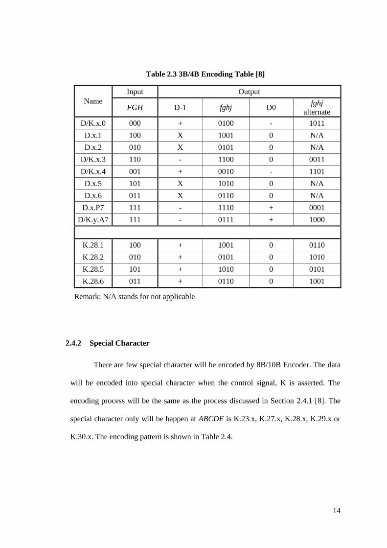
14
Table 2.3 3B/4B Encoding Table [8]
Name
Input Output
FGH D-1 fghj D0 fghj
alternate
D/K.x.0 000 + 0100 - 1011
D.x.1 100 X 1001 0 N/A
D.x.2 010 X 0101 0 N/A
D/K.x.3 110 - 1100 0 0011
D/K.x.4 001 + 0010 - 1101
D.x.5 101 X 1010 0 N/A
D.x.6 011 X 0110 0 N/A
D.x.P7 111 - 1110 + 0001
D/K.y.A7 111 - 0111 + 1000
K.28.1 100 + 1001 0 0110
K.28.2 010 + 0101 0 1010
K.28.5 101 + 1010 0 0101
K.28.6 011 + 0110 0 1001
Remark: N/A stands for not applicable
2.4.2 Special Character
There are few special character will be encoded by 8B/10B Encoder. The data
will be encoded into special character when the control signal, K is asserted. The
encoding process will be the same as the process discussed in Section 2.4.1 [8]. The
special character only will be happen at ABCDE is K.23.x, K.27.x, K.28.x, K.29.x or
K.30.x. The encoding pattern is shown in Table 2.4.
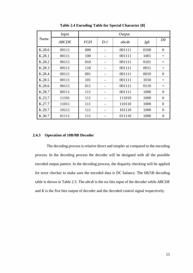
15
Table 2.4 Encoding Table for Special Character [8]
Name
Input Output
ABCDE FGH D-1 abcde fgh D0
K.28.0 00111 000 - 001111 0100 0
K.28.1 00111 100 - 001111 1001 +
K.28.2 00111 010 - 001111 0101 +
K.28.3 00111 110 - 001111 0011 +
K.28.4 00111 001 - 001111 0010 0
K.28.5 00111 101 - 001111 1010 +
K.28.6 00111 011 - 001111 0110 +
K.28.7 00111 111 - 001111 1000 0
K.23.7 11101 111 - 111010 1000 0
K.27.7 11011 111 - 110110 1000 0
K.29.7 10111 111 - 101110 1000 0
K.30.7 01111 111 - 011110 1000 0
2.4.3 Operation of 10B/8B Decoder
The decoding process is relative direct and simpler as compared to the encoding
process. In the decoding process the decoder will be designed with all the possible
encoded output pattern. In the decoding process, the disparity checking will be applied
for error checker to make sure the encoded data is DC balance. The 6B/5B decoding
table is shown in Table 2.5. The abcdi is the six bits input of the decoder while ABCDE
and K is the five bits output of decoder and the decoded control signal respectively.
16
Table 2.5 6B/5B Decoding Table [8]
Name Input Output
abcdi ABCDE K
D.0 011000
00000 0
100111 0
D.1 100010
10000 0
011101 0
D.2 010010
01000 0
101101 0
D.3 110001 11000 0
D.4 001010
00100 0
110101 0
D.5 101001 10100 0
D.6 011001 01100 0
D.7 111000
11100 0
000111 0
D.8 000110
00010 0
111001 0
D.9 100101 10010 0
D.10 010101 01010 0
D.11 110100 11010 0
D.12 001101 00110 0
D.13 101100 10110 0
D.14 011100 01110 0
D.15 101000
11110 0
010111 0
D.16 011011
00001 0
100100 0
D.17 100011 10001 0
D.18 010011 01001 0
D.19 110010 11001 0
D.20 001011 00101 0
D.21 101010 10101 0
D.22 011010 01101 0
D/K.23 111010
11101 X
000101 X
D.24 001100 00011 0
17
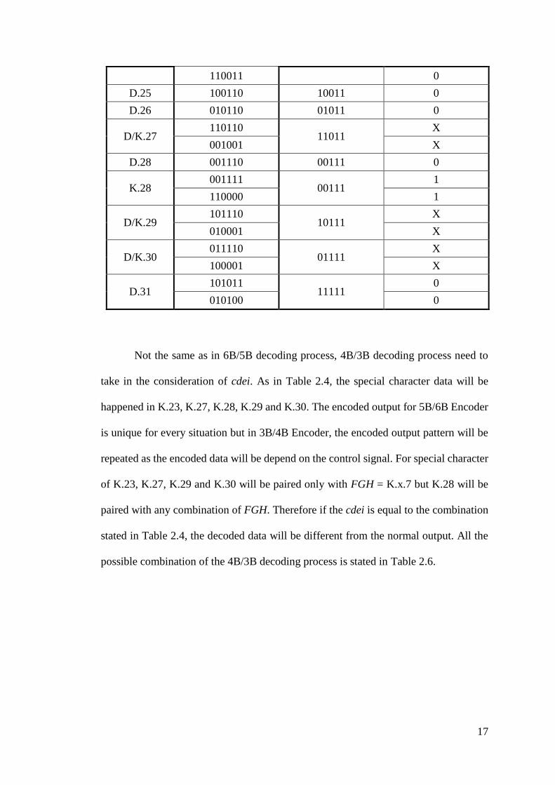
110011 0
D.25 100110 10011 0
D.26 010110 01011 0
D/K.27 110110
11011 X
001001 X
D.28 001110 00111 0
K.28 001111
00111 1
110000 1
D/K.29 101110
10111 X
010001 X
D/K.30 011110
01111 X
100001 X
D.31 101011
11111 0
010100 0
Not the same as in 6B/5B decoding process, 4B/3B decoding process need to
take in the consideration of cdei. As in Table 2.4, the special character data will be
happened in K.23, K.27, K.28, K.29 and K.30. The encoded output for 5B/6B Encoder
is unique for every situation but in 3B/4B Encoder, the encoded output pattern will be
repeated as the encoded data will be depend on the control signal. For special character
of K.23, K.27, K.29 and K.30 will be paired only with FGH = K.x.7 but K.28 will be
paired with any combination of FGH. Therefore if the cdei is equal to the combination
stated in Table 2.4, the decoded data will be different from the normal output. All the
possible combination of the 4B/3B decoding process is stated in Table 2.6.
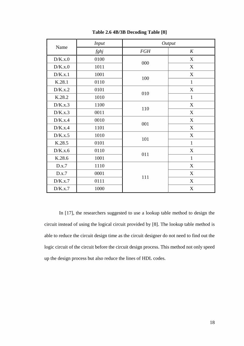
18
Table 2.6 4B/3B Decoding Table [8]
Name Input Output
fghj FGH K
D/K.x.0 0100 000
X
D/K.x.0 1011 X
D/K.x.1 1001 100
X
K.28.1 0110 1
D/K.x.2 0101 010
X
K.28.2 1010 1
D/K.x.3 1100 110
X
D/K.x.3 0011 X
D/K.x.4 0010 001
X
D/K.x.4 1101 X
D/K.x.5 1010 101
X
K.28.5 0101 1
D/K.x.6 0110 011
X
K.28.6 1001 1
D.x.7 1110
111
X
D.x.7 0001 X
D/K.x.7 0111 X
D/K.x.7 1000 X
In [17], the researchers suggested to use a lookup table method to design the
circuit instead of using the logical circuit provided by [8]. The lookup table method is
able to reduce the circuit design time as the circuit designer do not need to find out the
logic circuit of the circuit before the circuit design process. This method not only speed
up the design process but also reduce the lines of HDL codes.
19
2.5 Power Reduction Techniques
The total power consumption of a digital circuit is defined as[18]:
𝑃𝑡 = 𝑃𝑠𝑡𝑎𝑡𝑖𝑐 + 𝑃𝑑𝑦𝑛 (2.2)
Where:
𝑃𝑡 is the total power consumption of the circuit,
𝑃𝑠𝑡𝑎𝑡𝑖𝑐 is the static power of the circuit,
𝑃𝑑𝑦𝑛 is the dynamic power of the circuit
The static power is due to the leakage current of the transistor, steady state
current and etc. The general equations of the static power is:
𝑃𝑠𝑡𝑎𝑡𝑖𝑐 = 𝑉𝑐𝑐𝐼𝑐𝑐 (2.3)
Where:
𝑉𝑐𝑐 is the voltage supply to the circuit,
𝐼𝑐𝑐 is the current to the circuit
While dynamic power is due to the switching activity of the transistor such as
clock switching and dynamic power is defined as [19]:
𝑃𝑑𝑦𝑛 = 𝛼𝑓𝐶𝑉𝑑𝑑2 (2.4)
Where:
𝛼 is the switching activity factor,
20
𝑓 is the switching frequency
𝐶 is the capacitance of the circuit,
𝑉𝑑𝑑 is the voltage source of the circuit
Dynamic power will be the critical power that is needed to be reduced [20]. The
clock switching will cause the transistors to switch on and off, extra power is needed to
carry out in this activity and thus consume more power in the chip. The power
consumption by the clock switching activity is called clock power. The more switching
activities happen in the circuit, the more power will be needed by the circuit, as the
digital circuit needs to carry out logical operations even though the input data or the
data will not needed to process by the circuit. The overall power consumption (included
clock power) by the circuit or component is called hierarchy power. Therefore, to
reduce the power consumption, the switching activity or the voltage source supply
should be limit at a reasonable state.
2.5.1 Multi Voltage Source
Multi voltage source is used to reduce the wasted power of a system or circuit.
This can be done when a system has multiple intellectual property (IP) is grouped under
the same partition but different IP will be used at different level of voltage or power. If
only one source of voltage, the lower level voltage source consumers will be wasting
the power supply to it [21]. The voltage level shifter can be designed to shift the high
level power supply to low level supply [22–25].
21
In [21], the multi voltage source is applied to 16 nm Processor. The result
showing 54% of power reductions. The lower voltage source is applied to the lower
performance requirement IPs, and higher voltage source only applied to the higher
performance requirement IPs. This method can effectively distribute the power source
to the IPs without wasting the unnecessary power but it will also create extra area in the
circuit. As in [21], the area is increased 49% of the standard processor area, as the
retention register is needed in the circuit to distribute the power source to the IPs.
On the other hand, this method is more effectively to be done at circuit
implementation stage, as the same group of IPs will be group together and easier for
power planning. In this project, this method is not suitable to be implemented to the
circuit. This is because, the encoder design will be done up until Verilog HDL coding
and simulation stage, circuit implementation will not be carried out.
2.5.2 Power Gating
Power gating is another method can be implemented in circuit to reduce the
power consumption. This technique is used to shut down the non-operational part of
the circuit. This may reduce the power leakage of the static circuit [26]. The power
gating act as a switch to switch on and off the power supply to a non-functional group
of circuits and reduce the power consumption of the system [27–29].
In [26], the authors implemented the power gating circuit in to the Network-on-
Chip to shut down the power to those idle components. The results show that 18%
power consumption has been reduced by the power gating circuit. Although the power
gating circuit is able to reduce the power consumption, the results shows also the
perfomace degradation of the chip.
22
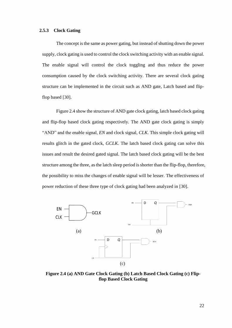
2.5.3 Clock Gating
The concept is the same as power gating, but instead of shutting down the power
supply, clock gating is used to control the clock switching activity with an enable signal.
The enable signal will control the clock toggling and thus reduce the power
consumption caused by the clock switching activity. There are several clock gating
structure can be implemented in the circuit such as AND gate, Latch based and flip-
flop based [30].
Figure 2.4 show the structure of AND gate clock gating, latch based clock gating
and flip-flop based clock gating respectively. The AND gate clock gating is simply
“AND” and the enable signal, EN and clock signal, CLK. This simple clock gating will
results glitch in the gated clock, GCLK. The latch based clock gating can solve this
issues and result the desired gated signal. The latch based clock gating will be the best
structure among the three, as the latch sleep period is shorter than the flip-flop, therefore,
the possibility to miss the changes of enable signal will be lesser. The effectiveness of
power reduction of these three type of clock gating had been analyzed in [30].
(a) (b)
(c)
Figure 2.4 (a) AND Gate Clock Gating (b) Latch Based Clock Gating (c) Flip-
flop Based Clock Gating

23
Therefore, the latch based signal will be implemented with the 8B/10B Encoder
and 10B/8B Decoder by using the gated clock signal instead of directly using the clock
source. This may improve the power performance of the circuit. The clock gating
implementation in 8B/10B Encoder and 10B/8B Decoder were carried out by [4, 29–
32].
In [4], the clock gated circuit reduce the encoder’s hierarchy power by 50% and
55.23% at 20 MHz and 200 MHz respectively. While the hierarchy power of clock
gated decoder’s circuit is reduced by 0% for both 20 MHz and 200 MHz. In the design,
the authors implemented a clock gating using negative latch. With this method, the
clock gating circuit not only limit the clock activities of the encoder but also limit the
clock activities of the clock gating circuit itself, as a result, more power consumption
is reduced by the clock gate.
2.6 Summary
The limited run length, DC balance and easiness of clock recovery are the
important characteristic and reason for 8B/10B to become popular recently. In the era
of small device, the power consumption is one of the element that researches are
focusing on. High speed application will consume more power as compared to low
speed application as the clock switching is more frequent. Thus, the clock gating is a
better choice to reduce the 8B/10B Encoder and 10B/8B Decoder. The second reason
of choosing clock gating over multi voltage source and power gating is because the
clock gating cell will not impact the area as the multi voltage source and power gating
does. Only a simple latch and AND gate are able to reduce the power consumption by

24
more than 50% as shown in the results of the research in [4]. In this project, a normal
latch and AND gate is used to form the clock gating cell.


![10B-LR 10B-SUB - Bryston10B].pdf · The 10B crossover is available in three stock versions; 10B-SUB incorporating frequencies more ... MONO LOW PASS MODE (10B-SUB AND 10B-STD ONLY):](https://static.fdocuments.net/doc/165x107/5afd7a367f8b9a434e8d9dda/10b-lr-10b-sub-10bpdfthe-10b-crossover-is-available-in-three-stock-versions.jpg)