Low-Power Analog Circuits for Sub-Band Speech Processing
75
Graduate Theses, Dissertations, and Problem Reports 2010 Low-Power Analog Circuits for Sub-Band Speech Processing Low-Power Analog Circuits for Sub-Band Speech Processing Anvesh Kumar Singireddy West Virginia University Follow this and additional works at: https://researchrepository.wvu.edu/etd Recommended Citation Recommended Citation Singireddy, Anvesh Kumar, "Low-Power Analog Circuits for Sub-Band Speech Processing" (2010). Graduate Theses, Dissertations, and Problem Reports. 4657. https://researchrepository.wvu.edu/etd/4657 This Thesis is protected by copyright and/or related rights. It has been brought to you by the The Research Repository @ WVU with permission from the rights-holder(s). You are free to use this Thesis in any way that is permitted by the copyright and related rights legislation that applies to your use. For other uses you must obtain permission from the rights-holder(s) directly, unless additional rights are indicated by a Creative Commons license in the record and/ or on the work itself. This Thesis has been accepted for inclusion in WVU Graduate Theses, Dissertations, and Problem Reports collection by an authorized administrator of The Research Repository @ WVU. For more information, please contact [email protected].
Transcript of Low-Power Analog Circuits for Sub-Band Speech Processing
Graduate Theses, Dissertations, and Problem Reports
2010
Low-Power Analog Circuits for Sub-Band Speech Processing Low-Power Analog Circuits for Sub-Band Speech Processing
Anvesh Kumar Singireddy West Virginia University
Follow this and additional works at: https://researchrepository.wvu.edu/etd
Recommended Citation Recommended Citation Singireddy, Anvesh Kumar, "Low-Power Analog Circuits for Sub-Band Speech Processing" (2010). Graduate Theses, Dissertations, and Problem Reports. 4657. https://researchrepository.wvu.edu/etd/4657
This Thesis is protected by copyright and/or related rights. It has been brought to you by the The Research Repository @ WVU with permission from the rights-holder(s). You are free to use this Thesis in any way that is permitted by the copyright and related rights legislation that applies to your use. For other uses you must obtain permission from the rights-holder(s) directly, unless additional rights are indicated by a Creative Commons license in the record and/ or on the work itself. This Thesis has been accepted for inclusion in WVU Graduate Theses, Dissertations, and Problem Reports collection by an authorized administrator of The Research Repository @ WVU. For more information, please contact [email protected].
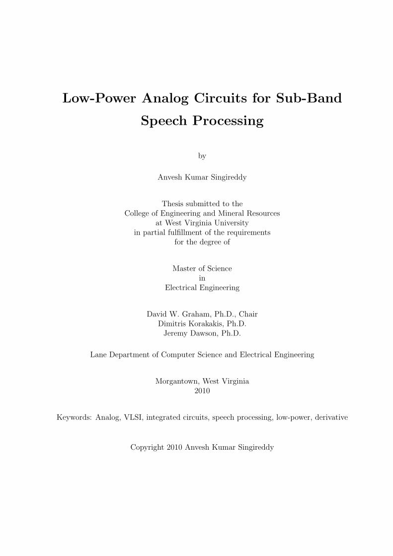
Low-Power Analog Circuits for Sub-Band
Speech Processing
by
Anvesh Kumar Singireddy
Thesis submitted to theCollege of Engineering and Mineral Resources
at West Virginia Universityin partial fulfillment of the requirements
for the degree of
Master of Sciencein
Electrical Engineering
David W. Graham, Ph.D., ChairDimitris Korakakis, Ph.D.
Jeremy Dawson, Ph.D.
Lane Department of Computer Science and Electrical Engineering
Morgantown, West Virginia2010
Keywords: Analog, VLSI, integrated circuits, speech processing, low-power, derivative
Copyright 2010 Anvesh Kumar Singireddy

Abstract
Low-Power Analog Circuits for Sub-Band Speech Processing
by
Anvesh Kumar SingireddyMaster of Science in Electrical Engineering
West Virginia University
David W. Graham, Ph.D., Chair
The need for efficient electronics has been increasing by the day, as have the constraintson power and size of the devices. Also the increase in use of mobile and wearable electronicshas been leading to innovative methods to conserve power and increase functionality. Thetraditional approach of signal processing heavily relies on the Digital Signal Processing (DSP)hardware to perform most of the tasks, which has lead to power-hungry circuits. Use ofanalog front-end devices could prove to be efficient, since most of the real-world data isanalog and since the DSP could be spared for more application-specific tasks within thesystem, thereby resulting in more efficient mixed-signal systems.
The focus in this work is to develop an analog front-end for speech-processing applicationswith inspiration from biology, and trying to mimic human auditory perception techniques.The circuits are designed in 600nm, 350nm and 180nm CMOS processes and are biasedin the sub-threshold region to consume low-power. Also, various modules of the systemare connected using multiplexing circuits to allow post-fabrication reconfigurability to suitvarious applications. These circuits are biased using a network of floating-gate transistorswhich allow reconfigurability and increased bias accuracy. This thesis mainly describes twomodules of the analog front-end used for speech processing: derivative circuit and voltage-mode subtractor circuit, which are used for processing spectrally decomposed signals. Thesecircuits could be used for applications like audio analysis or event detection.

iii
Acknowledgments
I want to thank my advisor, Dr. David Graham, for his encouragement, knowledge
and support throughout my graduate studies here at West Virginia University. I also want
to thank the rest of my committee, Dr. Dimitris Korakakis and Dr. Jeremy Dawson, for
lending their expertise on the periphery of this research area. Thanks to GTronix for partially
funding this project and for their valuable feedback. I also want to acknowledge Brandon
Rumberg, who worked on the other half of this project. Also, a big thanks to my family and
friends, without whom I could not have come so far.
iv
Contents
Acknowledgments iii
List of Figures vi
1 Introduction 11.1 Analog Front-ends . . . . . . . . . . . . . . . . . . . . . . . . . . . . . . . . 2
1.1.1 Differentiator . . . . . . . . . . . . . . . . . . . . . . . . . . . . . . . 41.1.2 Subtractor . . . . . . . . . . . . . . . . . . . . . . . . . . . . . . . . . 51.1.3 Floating-gate Transistors . . . . . . . . . . . . . . . . . . . . . . . . . 51.1.4 Filter-Bank with Sub-band Processing . . . . . . . . . . . . . . . . . 6
1.2 Basic Building Blocks . . . . . . . . . . . . . . . . . . . . . . . . . . . . . . . 61.3 Organization . . . . . . . . . . . . . . . . . . . . . . . . . . . . . . . . . . . 7
2 Derivative Circuit 92.1 Different Kinds of Derivative Models . . . . . . . . . . . . . . . . . . . . . . 10
2.1.1 First-Order High-Pass Filter . . . . . . . . . . . . . . . . . . . . . . . 102.1.2 Capacitor for Derivative . . . . . . . . . . . . . . . . . . . . . . . . . 122.1.3 Current-Output Derivative Circuits . . . . . . . . . . . . . . . . . . . 162.1.4 Differently-Clamped-Capacitor based Differentiator . . . . . . . . . . 17
2.2 Design of Differentiator Circuit . . . . . . . . . . . . . . . . . . . . . . . . . 182.2.1 Various Blocks of the Differentiator Circuit . . . . . . . . . . . . . . . 222.2.2 Results from the Differentiator Circuit . . . . . . . . . . . . . . . . . 25
3 Subtractor Circuit 293.1 Basic Principle . . . . . . . . . . . . . . . . . . . . . . . . . . . . . . . . . . 293.2 Design of Subtractor Circuit . . . . . . . . . . . . . . . . . . . . . . . . . . . 30
3.2.1 Working of Subtractor Circuit . . . . . . . . . . . . . . . . . . . . . . 313.2.2 Output Limitations . . . . . . . . . . . . . . . . . . . . . . . . . . . . 33
3.3 Results . . . . . . . . . . . . . . . . . . . . . . . . . . . . . . . . . . . . . . . 33
4 Floating-Gate Tranistors 414.1 Floating-Gate Transistors . . . . . . . . . . . . . . . . . . . . . . . . . . . . 41
4.1.1 Electron Injection . . . . . . . . . . . . . . . . . . . . . . . . . . . . . 424.1.2 Electron Tunneling . . . . . . . . . . . . . . . . . . . . . . . . . . . . 444.1.3 Tunneling Junction . . . . . . . . . . . . . . . . . . . . . . . . . . . . 46
CONTENTS v
5 Analog Auditory Front-End 485.1 Working of Analog Auditory Front-End . . . . . . . . . . . . . . . . . . . . . 48
6 Applications and Conclusion 536.1 Low-Power Hardware-Based Event Detection . . . . . . . . . . . . . . . . . . 536.2 Design of the Analog System . . . . . . . . . . . . . . . . . . . . . . . . . . . 54
6.2.1 Single-Dimensional Sound Localization . . . . . . . . . . . . . . . . . 546.2.2 Sound/Event Classification . . . . . . . . . . . . . . . . . . . . . . . . 55
6.3 Conclusion . . . . . . . . . . . . . . . . . . . . . . . . . . . . . . . . . . . . . 56
A Cadence setup 59
B More Derivative Circuit Models 60B.1 Hysteretic Differentiators . . . . . . . . . . . . . . . . . . . . . . . . . . . . . 60B.2 RL-Type Differentiators . . . . . . . . . . . . . . . . . . . . . . . . . . . . . 61
References 64
Approval Page 66
vi
List of Figures
1.1 Analog and digital systems . . . . . . . . . . . . . . . . . . . . . . . . . . . . 31.2 Block diagram of the analog front-end . . . . . . . . . . . . . . . . . . . . . 31.3 A real-time system with analog front-end. . . . . . . . . . . . . . . . . . . . 41.4 Floating-gate symbol . . . . . . . . . . . . . . . . . . . . . . . . . . . . . . . 51.5 Transistor symbols . . . . . . . . . . . . . . . . . . . . . . . . . . . . . . . . 7
2.1 Differentiation of a sine wave (simulated) . . . . . . . . . . . . . . . . . . . . 102.2 Ideal frequency response of a differentiator (simulated) . . . . . . . . . . . . 112.3 Variation of gain with capacitor size . . . . . . . . . . . . . . . . . . . . . . . 122.4 Differentiator using RC-like filter . . . . . . . . . . . . . . . . . . . . . . . . 132.5 Frequency response of a differentiator using RC-like filter . . . . . . . . . . . 142.6 Grounded Capacitor and Clamped capacitor methodss . . . . . . . . . . . . 152.7 Follower integrator circuit . . . . . . . . . . . . . . . . . . . . . . . . . . . . 152.8 The diff1 circuit . . . . . . . . . . . . . . . . . . . . . . . . . . . . . . . . . . 162.9 The diff2 circuit . . . . . . . . . . . . . . . . . . . . . . . . . . . . . . . . . . 162.10 Frequency response of diff2 (simulated) . . . . . . . . . . . . . . . . . . . . . 172.11 Varying bias conditions versus Diff2 frequency resposne . . . . . . . . . . . . 182.12 Current output based differentiator . . . . . . . . . . . . . . . . . . . . . . . 192.13 Basic idea for differentiation . . . . . . . . . . . . . . . . . . . . . . . . . . . 192.14 Limiter circuit . . . . . . . . . . . . . . . . . . . . . . . . . . . . . . . . . . . 202.15 Frequency response of clamped capacitor based differentiator (simulated) . . 202.16 Feed-back and feed-forward differentiator models . . . . . . . . . . . . . . . . 212.17 The basic differentiator circuit . . . . . . . . . . . . . . . . . . . . . . . . . . 222.18 The improvised differentiator circuit . . . . . . . . . . . . . . . . . . . . . . . 232.19 The Tobi element . . . . . . . . . . . . . . . . . . . . . . . . . . . . . . . . . 242.20 Layout of differentiator block . . . . . . . . . . . . . . . . . . . . . . . . . . 242.21 Demonstration of Sine to Cosine conversion . . . . . . . . . . . . . . . . . . 262.22 Frequency response of differentiator circuit . . . . . . . . . . . . . . . . . . . 272.23 Noise power in the output of differentiator circuit . . . . . . . . . . . . . . . 282.24 THD of the differentiator circuit . . . . . . . . . . . . . . . . . . . . . . . . . 28
3.1 Basic idea for voltage-mode subtractor circuit . . . . . . . . . . . . . . . . . 303.2 Subtractor circuit . . . . . . . . . . . . . . . . . . . . . . . . . . . . . . . . . 323.3 Subtractor implentation . . . . . . . . . . . . . . . . . . . . . . . . . . . . . 34
LIST OF FIGURES vii
3.4 Layout of subtractor block . . . . . . . . . . . . . . . . . . . . . . . . . . . . 353.5 Voltage-mode subtraction of two sinusoidal signals . . . . . . . . . . . . . . . 363.6 Amplitude modulated signals through Subtractor circuit . . . . . . . . . . . 373.7 Error vs. Amplitude for Subtractor circuit . . . . . . . . . . . . . . . . . . . 373.8 Output Error relation with input DC level . . . . . . . . . . . . . . . . . . . 383.9 Output Error relation with output DC level . . . . . . . . . . . . . . . . . . 383.10 Frequency response of subtractor circuit . . . . . . . . . . . . . . . . . . . . 393.11 THD of subtractor circuit. . . . . . . . . . . . . . . . . . . . . . . . . . . . . 393.12 Noise power in the output of the subtractor circuit . . . . . . . . . . . . . . 403.13 Relation between SNR and bias voltage . . . . . . . . . . . . . . . . . . . . . 40
4.1 Floating gate and Control gate . . . . . . . . . . . . . . . . . . . . . . . . . 414.2 I-V relation with charge present on the floating gate . . . . . . . . . . . . . . 424.3 Drain current relation with floating-gate charge . . . . . . . . . . . . . . . . 434.4 Electron injection . . . . . . . . . . . . . . . . . . . . . . . . . . . . . . . . . 444.5 Electron tunneling . . . . . . . . . . . . . . . . . . . . . . . . . . . . . . . . 454.6 Comparison of tunneling times for MOScap and Varactor tunneling junctions 464.7 Layout of MOSCAP based tunneling junction . . . . . . . . . . . . . . . . . 474.8 Layout of varactor based tunneling junction . . . . . . . . . . . . . . . . . . 47
5.1 C4 frequency response. . . . . . . . . . . . . . . . . . . . . . . . . . . . . . . 495.2 Response of the magnitude detector circuit (simulated). . . . . . . . . . . . . 505.3 Transient response of differentiator circuit . . . . . . . . . . . . . . . . . . . 505.4 Transient response of subtractor circuit (simulated). . . . . . . . . . . . . . . 515.5 Single column of the analog front-end . . . . . . . . . . . . . . . . . . . . . . 515.6 Layout of the 0.18µm auditory front-end . . . . . . . . . . . . . . . . . . . . 52
6.1 Idea for hardware detection of sound events. . . . . . . . . . . . . . . . . . . 546.2 Peak detector prototype with discrete components . . . . . . . . . . . . . . . 556.3 Power consumption comparison in analog and digital systems . . . . . . . . . 566.4 Block diagram for the fabricated event detection system. . . . . . . . . . . . 576.5 Die shot of the event detection chip . . . . . . . . . . . . . . . . . . . . . . . 58
B.1 Hysteretic differentiator circuit . . . . . . . . . . . . . . . . . . . . . . . . . 60B.2 Different versions of hysteretic differentiator circuit . . . . . . . . . . . . . . 62B.3 The RL-type differentiator . . . . . . . . . . . . . . . . . . . . . . . . . . . . 63
1
Chapter 1
Introduction
Most circuits in contemporary VLSI systems are designed with digital technology as their
basis. But computations, such as addition, subtraction, multiplication, differentiation and
integration, are more suitable for analog circuits at a macroscopic level [1]. For example,
a high quality microphone deployed to pick up sound from a musical concert generates a
signal whose amplitude may vary from few microvolts to hundreds of microvolts. For exten-
sive sound processing, all such signals go through significant processing using a digital signal
processor (DSP). But these signals almost always are either too small for digitization or have
unwanted out-of-band signals and noise associated with them. Due to this, the introduc-
tion of a modified analog front-end could enhance the signal quality. Also, these front-end
operations can be performed using only a few transistors [2]. Along with the advantage of
low-power consumption of circuits that operate in sub-threshold or weak inversion regions,
analog systems can also describe naturally occurring systems more closely than the digital
systems.
With progress in semiconductor research leading to smaller chip sizes and the increased
use of small and mobile electronic devices, low-power systems have gained importance. Most
modern electronic devices require significant processing capability to support the various
applications they are used for, hence, leading to higher power consumption. Using analog
systems operating in weak inversion region as a front-end for tasks like speech-recognition
or environment sensing would greatly reduce the power needs of the devices. Mainly, these
kind of devices would be useful in hearing aids, audio analysis and situations like remote
Anvesh K. Singireddy Chapter 1. Introduction 2
monitoring where human presence needs to be avoided or would not be feasible. The main
idea behind this kind of speech processing system is to closely replicate the signals produced
by a human brain while processing auditory information it receives through the cochlea. So
for the device to perform like human to perceive the environment, designing systems that
mimic the human biology would be logical. Moreover, biology provides examples of very
efficient perception systems, so trying to replicate, or at least come close, would present us
with very efficient systems [3].
The objective of this overreaching project is to develop a speech-processing front-end,
which can process auditory information, extract certain application specific features, and
reduce the burden on the next level of digital processing systems.
1.1 Analog Front-ends
In a typical real-time system, the transducer produces current or voltage signals depend-
ing on the changes in its environment. These signals are mostly in varying time intervals and
varying magnitude depending on the input the transducer receives. The output signals from
the transducers are later processed by digital signal processors (DSPs) after being converted
to digital signals using an analog to digital converter (ADC). A lot of computational power
would be required to process all the data that the transducers dump onto the DSP. Using
a few custom-built circuits to properly decompose the raw data from the transducer would
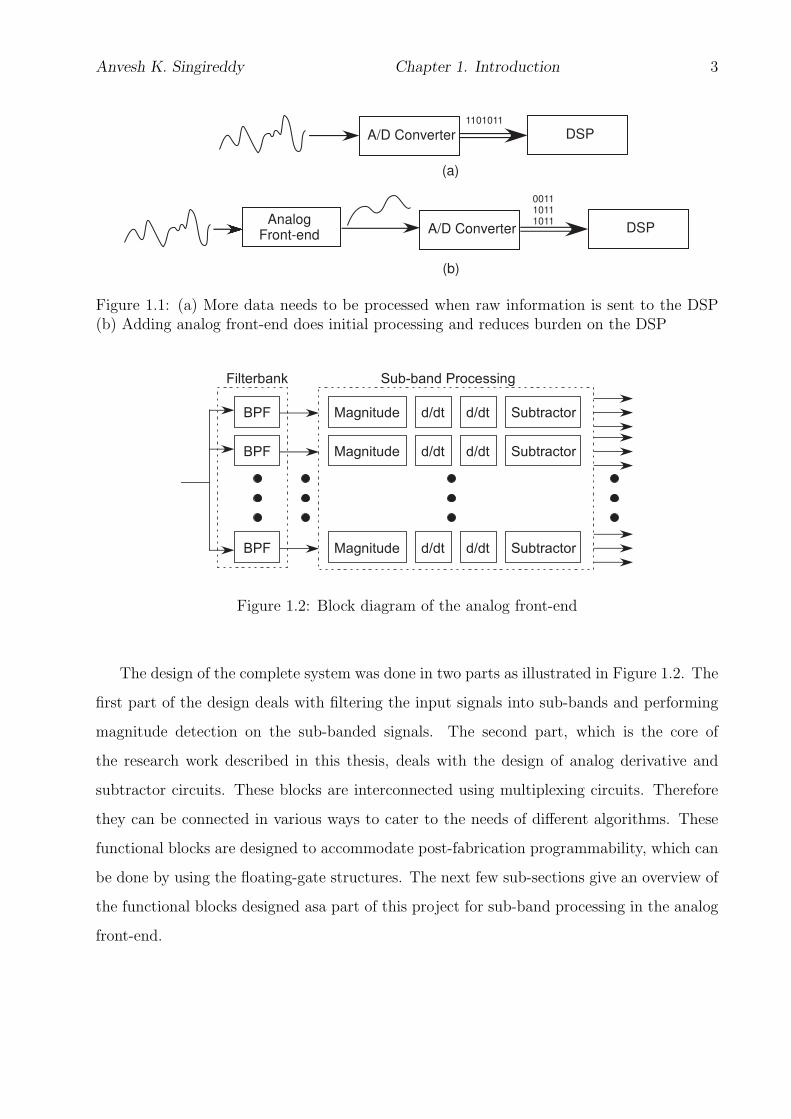
greatly reduce the burden on the power-hungry DSPs (Fig. 1.1).
The focus of this project is to design such custom-built circuits for band-pass filtering
of speech signals while adding specific computational capability to the circuits. The main
aim here is to produce a few compact circuits with low-power consumption, allowing highly-
parallel systems used in real-time data collection and processing. For this particular project,
a large number of computations are done on raw data normally by the digital end. This
could easily be done by an analog system (Fig. 1.3). Also, this analog system will have
continous-time circuits for real-time operation. This new model could lead to lower power
consumption as the transistors are biased in sub-threshold and also they could be more
efficient [3].
Anvesh K. Singireddy Chapter 1. Introduction 3
A/D Converter
1101011
DSP
(a)
A/D Converter
0011 1011 1011
DSPAnalog
Front-end
(b)
Figure 1.1: (a) More data needs to be processed when raw information is sent to the DSP(b) Adding analog front-end does initial processing and reduces burden on the DSP
BPF Magnitude d/dt Subtractord/dt
BPF Magnitude d/dt Subtractord/dt
BPF Magnitude d/dt Subtractord/dt
Filterbank Sub-band Processing
Figure 1.2: Block diagram of the analog front-end
The design of the complete system was done in two parts as illustrated in Figure 1.2. The
first part of the design deals with filtering the input signals into sub-bands and performing
magnitude detection on the sub-banded signals. The second part, which is the core of
the research work described in this thesis, deals with the design of analog derivative and
subtractor circuits. These blocks are interconnected using multiplexing circuits. Therefore
they can be connected in various ways to cater to the needs of different algorithms. These
functional blocks are designed to accommodate post-fabrication programmability, which can
be done by using the floating-gate structures. The next few sub-sections give an overview of
the functional blocks designed asa part of this project for sub-band processing in the analog
front-end.
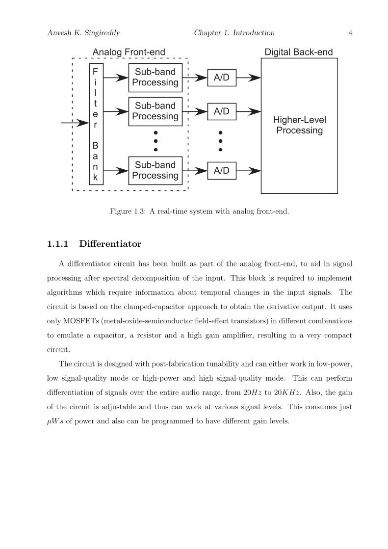
Anvesh K. Singireddy Chapter 1. Introduction 4
Sub-band Processing
A/D
Higher-Level Processing
Analog Front-end Digital Back-end
Sub-band Processing
Sub-band Processing
F i l t e r
B a n k
A/D
A/D
Figure 1.3: A real-time system with analog front-end.
1.1.1 Differentiator
A differentiator circuit has been built as part of the analog front-end, to aid in signal
processing after spectral decomposition of the input. This block is required to implement
algorithms which require information about temporal changes in the input signals. The
circuit is based on the clamped-capacitor approach to obtain the derivative output. It uses
only MOSFETs (metal-oxide-semiconductor field-effect transistors) in different combinations
to emulate a capacitor, a resistor and a high gain amplifier, resulting in a very compact
circuit.
The circuit is designed with post-fabrication tunability and can either work in low-power,
low signal-quality mode or high-power and high signal-quality mode. This can perform
differentiation of signals over the entire audio range, from 20Hz to 20KHz. Also, the gain
of the circuit is adjustable and thus can work at various signal levels. This consumes just
µWs of power and also can be programmed to have different gain levels.
Anvesh K. Singireddy Chapter 1. Introduction 5
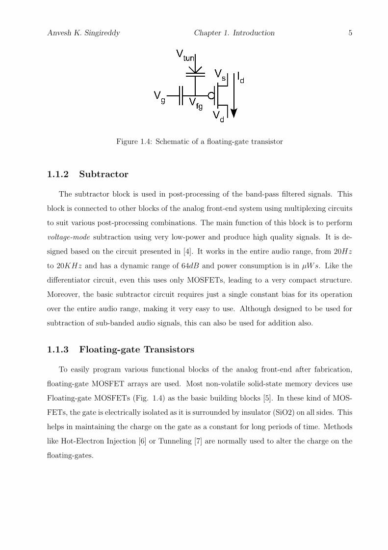
Figure 1.4: Schematic of a floating-gate transistor
1.1.2 Subtractor
The subtractor block is used in post-processing of the band-pass filtered signals. This
block is connected to other blocks of the analog front-end system using multiplexing circuits
to suit various post-processing combinations. The main function of this block is to perform
voltage-mode subtraction using very low-power and produce high quality signals. It is de-
signed based on the circuit presented in [4]. It works in the entire audio range, from 20Hz
to 20KHz and has a dynamic range of 64dB and power consumption is in µWs. Like the
differentiator circuit, even this uses only MOSFETs, leading to a very compact structure.
Moreover, the basic subtractor circuit requires just a single constant bias for its operation
over the entire audio range, making it very easy to use. Although designed to be used for
subtraction of sub-banded audio signals, this can also be used for addition also.
1.1.3 Floating-gate Transistors
To easily program various functional blocks of the analog front-end after fabrication,
floating-gate MOSFET arrays are used. Most non-volatile solid-state memory devices use
Floating-gate MOSFETs (Fig. 1.4) as the basic building blocks [5]. In these kind of MOS-
FETs, the gate is electrically isolated as it is surrounded by insulator (SiO2) on all sides. This
helps in maintaining the charge on the gate as a constant for long periods of time. Methods
like Hot-Electron Injection [6] or Tunneling [7] are normally used to alter the charge on the
floating-gates.
Anvesh K. Singireddy Chapter 1. Introduction 6
As the gate of these transistors does not have any physical contact with other conductors
on the chip, the capacitively induced charge can be stored and used to set the bias for other
devices. The floating-gate MOSFETs can be used to precisely set the bias for operating the
systems reliably and efficiently. This gives the ability to program various functional blocks,
depending on the application. By suitably designing a matrix of these basic floating-gate
MOSFETs, the total analog front-end can be programed easily and efficiently. Also, this
helps to offset any mismatches during fabrication of the chips and leads to better quality
systems.
1.1.4 Filter-Bank with Sub-band Processing
The complete analog front-end comprises the functional blocks for spectral decomposi-
tion, magnitude detection, differentiation and subtraction. The complete system includes an
array of 16 channels of each of the analog front-ends. Each channel is used for sub-banding
and processing the audio signals of a particular frequency range within the audio range. The
total system was fabricated on a 0.18µm CMOS (complementary MOS) process and was
designed to have high flexibility of connections between each block post-fabrication. This
would allow to perform various applications depending on the requirement. Along with this,
one more filter-bank with reduced functionality and only 8 channels was used to design an
intelligent wireless analog event-detection system. This was done on a 0.5µm CMOS process.
These front-ends could be used in the future for applications like speech-recognition, audio
analysis or hardware-based event detection.
1.2 Basic Building Blocks
The main focus of this project was to build a low-power system, while having good
performance and signal quality. This system is intended to compliment the DSP, and help
reduce the burden on it, in turn, leading to lower power consumption. CMOS linear devices
and digital devices use the same fabrication process so the analog and digital systems can
be integrated onto a single chip, making the production easier and cheaper. Also, as the
range of applications performed by a chip increases, it would require both analog and digital
Anvesh K. Singireddy Chapter 1. Introduction 7
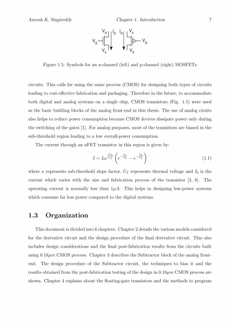
Vg
VdVs
Id IdVsVd
Vg
Figure 1.5: Symbols for an n-channel (left) and p-channel (right) MOSFETs
circuits. This calls for using the same process (CMOS) for designing both types of circuits
leading to cost-effective fabrication and packaging. Therefore in the future, to accommodate
both digital and analog systems on a single chip, CMOS transistors (Fig. 1.5) were used
as the basic building blocks of the analog front-end in this thesis. The use of analog ciruits
also helps to reduce power consumption because CMOS devices dissipate power only during
the switching of the gates [1]. For analog purposes, most of the transistors are biased in the
sub-threshold region leading to a low overall-power consumption.
The current through an nFET transistor in this region is given by:
I = I0eκVgUT
(e− Vs
UT − e− Vd
UT
)(1.1)
where κ represents sub-threshold slope factor, UT represents thermal voltage and I0 is the
current which varies with the size and fabrication process of the transistor [3, 8]. The
operating current is normally less than 1µA. This helps in designing low-power systems
which consume far less power compared to the digital systems.
1.3 Organization
This document is divided into 6 chapters. Chapter 2 details the various models considered
for the derivative circuit and the design procedure of the final derivative circuit. This also
includes design considerations and the final post-fabrication results from the circuits built
using 0.18µm CMOS process. Chapter 3 describes the Subtractor block of the analog front-
end. The design procedure of the Subtractor circuit, the techniques to bias it and the
results obtained from the post-fabrication testing of the design in 0.18µm CMOS process are
shown. Chapter 4 explains about the floating-gate transistors and the methods to program

Anvesh K. Singireddy Chapter 1. Introduction 8
and erase charge from the floating-gate. Chapter 5 deals with the overall function of the
analog front-end as a whole. The flow of signals between various blocks of the analog front-
end is discussed and explains how each block would fit in. It also gives the details of how
the floating gate structures were used to program various blocks of the analog front-end.
Chapter 6 discusses the application of the analog systems in wireless sensor networks to
reduce power conusmption and future scope of this work.
All the data presented in this thesis is from circuits fabricated in either 0.5µm or 0.18µm
CMOS process unless mentioned as simulated.
9
Chapter 2
Derivative Circuit
The derivative circuit designed as part of this project is used to implement various speech
processing algorithms on the audio signals after they have been spectrally decomposed. That
is, only the sub-banded signals would be fed as input to the derivative circuit. The circuit
helps in extracting the temporal change information from various band-passed signals in the
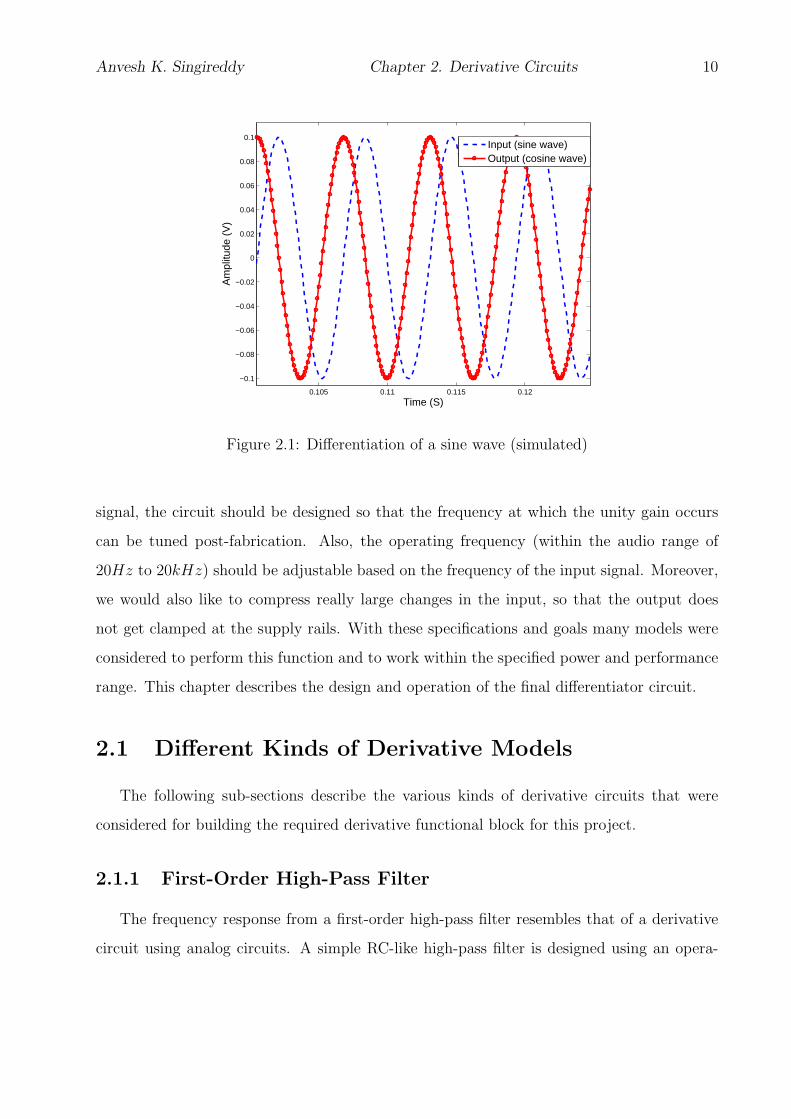
audio frequency range. To obtain the derivative of a sub-banded signal, the gain must be
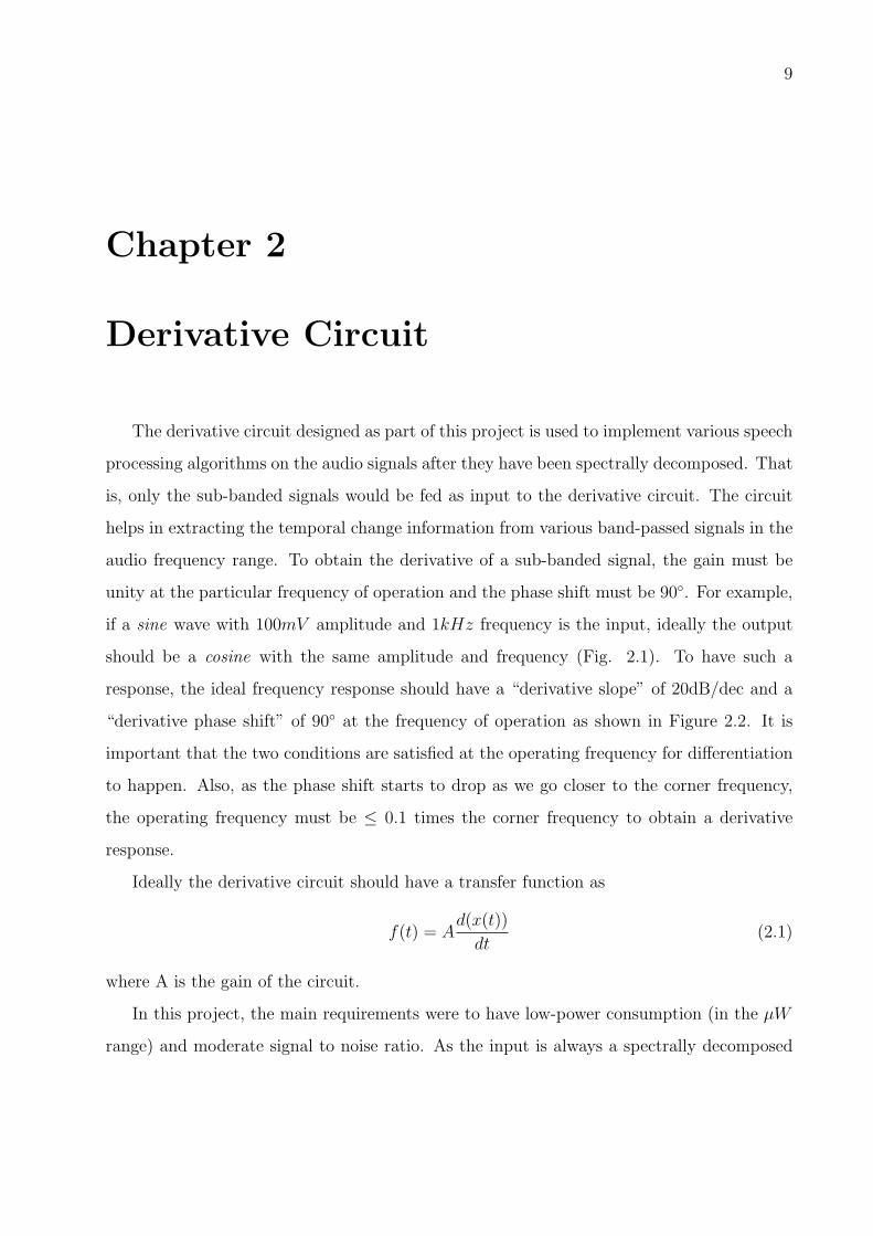
unity at the particular frequency of operation and the phase shift must be 90◦. For example,
if a sine wave with 100mV amplitude and 1kHz frequency is the input, ideally the output
should be a cosine with the same amplitude and frequency (Fig. 2.1). To have such a
response, the ideal frequency response should have a “derivative slope” of 20dB/dec and a
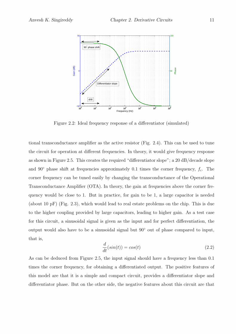
“derivative phase shift” of 90◦ at the frequency of operation as shown in Figure 2.2. It is
important that the two conditions are satisfied at the operating frequency for differentiation
to happen. Also, as the phase shift starts to drop as we go closer to the corner frequency,
the operating frequency must be ≤ 0.1 times the corner frequency to obtain a derivative
response.
Ideally the derivative circuit should have a transfer function as
f(t) = Ad(x(t))
dt(2.1)
where A is the gain of the circuit.
In this project, the main requirements were to have low-power consumption (in the µW
range) and moderate signal to noise ratio. As the input is always a spectrally decomposed
Anvesh K. Singireddy Chapter 2. Derivative Circuits 10
0.105 0.11 0.115 0.12
−0.1
−0.08
−0.06
−0.04
−0.02
0
0.02
0.04
0.06
0.08
0.1
Time (S)
Am
plitu
de (
V)
Input (sine wave)Output (cosine wave)
Figure 2.1: Differentiation of a sine wave (simulated)
signal, the circuit should be designed so that the frequency at which the unity gain occurs
can be tuned post-fabrication. Also, the operating frequency (within the audio range of
20Hz to 20kHz) should be adjustable based on the frequency of the input signal. Moreover,
we would also like to compress really large changes in the input, so that the output does
not get clamped at the supply rails. With these specifications and goals many models were
considered to perform this function and to work within the specified power and performance
range. This chapter describes the design and operation of the final differentiator circuit.
2.1 Different Kinds of Derivative Models
The following sub-sections describe the various kinds of derivative circuits that were
considered for building the required derivative functional block for this project.
2.1.1 First-Order High-Pass Filter
The frequency response from a first-order high-pass filter resembles that of a derivative
circuit using analog circuits. A simple RC-like high-pass filter is designed using an opera-
Anvesh K. Singireddy Chapter 2. Derivative Circuits 11
100
101
102
103
104
105
106
−50
0
50
Gai
n (d
B)
Frequency (Hz)10
010
110
210
310
410
510
60
50
100
Pha
se
Differentiator slope
d/dt
90° phase shift
Figure 2.2: Ideal frequency response of a differentiator (simulated)
tional transconductance amplifier as the active resistor (Fig. 2.4). This can be used to tune
the circuit for operation at different frequencies. In theory, it would give frequency response
as shown in Figure 2.5. This creates the required “differentiator slope”; a 20 dB/decade slope
and 90◦ phase shift at frequencies approximately 0.1 times the corner frequency, fc. The
corner frequency can be tuned easily by changing the transconductance of the Operational
Transconductance Amplifier (OTA). In theory, the gain at frequencies above the corner fre-
quency would be close to 1. But in practice, for gain to be 1, a large capacitor is needed
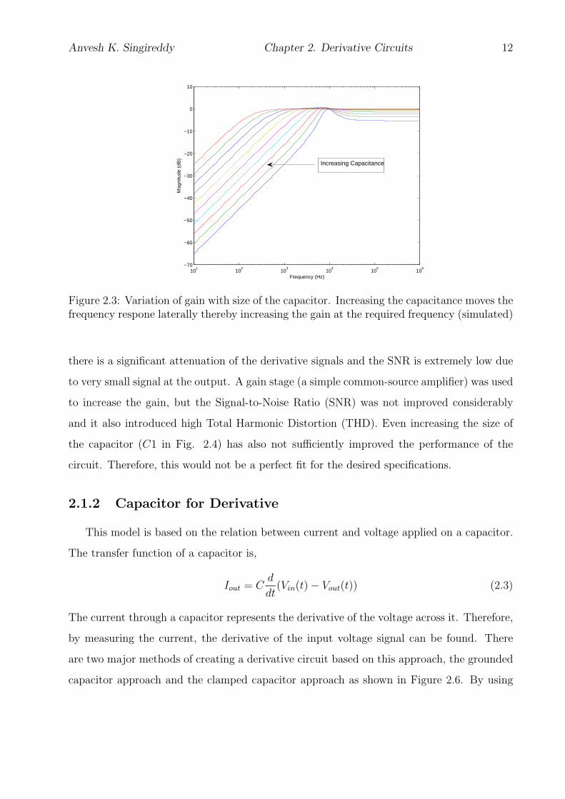
(about 10 pF) (Fig. 2.3), which would lead to real estate problems on the chip. This is due
to the higher coupling provided by large capacitors, leading to higher gain. As a test case
for this circuit, a sinusoidal signal is given as the input and for perfect differentiation, the
output would also have to be a sinusoidal signal but 90◦ out of phase compared to input,
that is,d
dt(sin(t)) = cos(t) (2.2)
As can be deduced from Figure 2.5, the input signal should have a frequency less than 0.1
times the corner frequency, for obtaining a differentiated output. The positive features of
this model are that it is a simple and compact circuit, provides a differentiator slope and
differentiator phase. But on the other side, the negative features about this circuit are that
Anvesh K. Singireddy Chapter 2. Derivative Circuits 12
101
102
103
104
105
106
−70
−60
−50
−40
−30
−20
−10
0
10
Frequency (Hz)
Mag
nitu
de (
dB)
Increasing Capacitance
Figure 2.3: Variation of gain with size of the capacitor. Increasing the capacitance moves thefrequency respone laterally thereby increasing the gain at the required frequency (simulated)
there is a significant attenuation of the derivative signals and the SNR is extremely low due
to very small signal at the output. A gain stage (a simple common-source amplifier) was used
to increase the gain, but the Signal-to-Noise Ratio (SNR) was not improved considerably
and it also introduced high Total Harmonic Distortion (THD). Even increasing the size of
the capacitor (C1 in Fig. 2.4) has also not sufficiently improved the performance of the
circuit. Therefore, this would not be a perfect fit for the desired specifications.
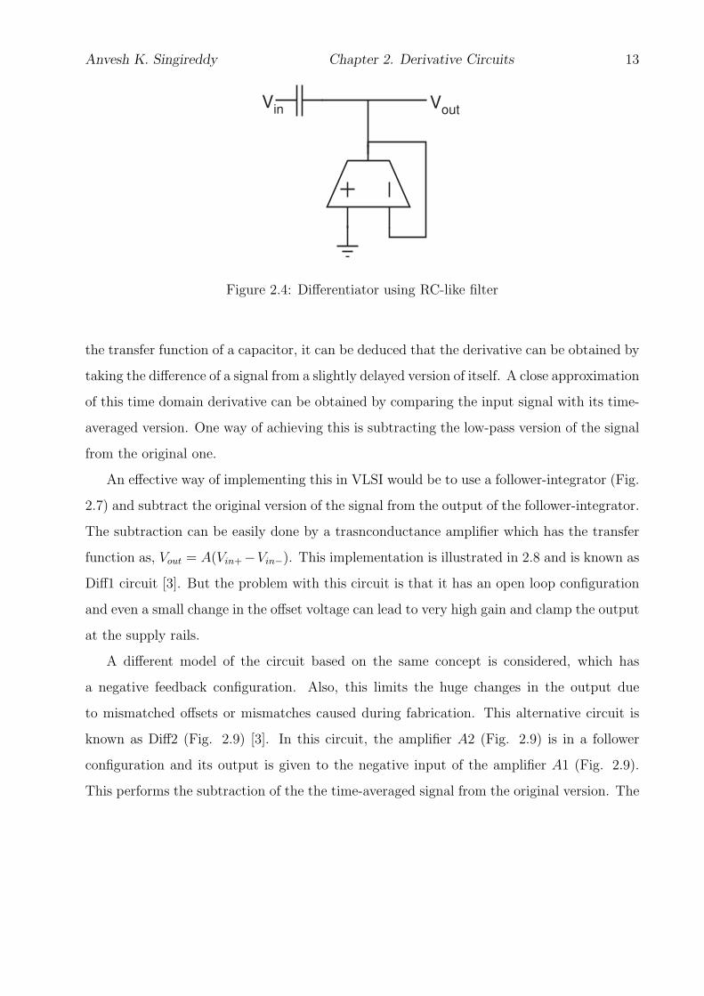
2.1.2 Capacitor for Derivative
This model is based on the relation between current and voltage applied on a capacitor.
The transfer function of a capacitor is,
Iout = Cd
dt(Vin(t) − Vout(t)) (2.3)
The current through a capacitor represents the derivative of the voltage across it. Therefore,
by measuring the current, the derivative of the input voltage signal can be found. There
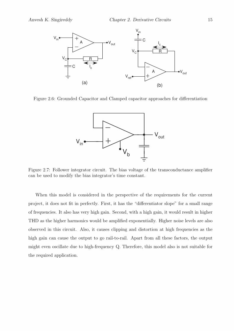
are two major methods of creating a derivative circuit based on this approach, the grounded
capacitor approach and the clamped capacitor approach as shown in Figure 2.6. By using
Anvesh K. Singireddy Chapter 2. Derivative Circuits 13
Vin
Vout
Figure 2.4: Differentiator using RC-like filter
the transfer function of a capacitor, it can be deduced that the derivative can be obtained by
taking the difference of a signal from a slightly delayed version of itself. A close approximation
of this time domain derivative can be obtained by comparing the input signal with its time-
averaged version. One way of achieving this is subtracting the low-pass version of the signal
from the original one.
An effective way of implementing this in VLSI would be to use a follower-integrator (Fig.
2.7) and subtract the original version of the signal from the output of the follower-integrator.
The subtraction can be easily done by a trasnconductance amplifier which has the transfer
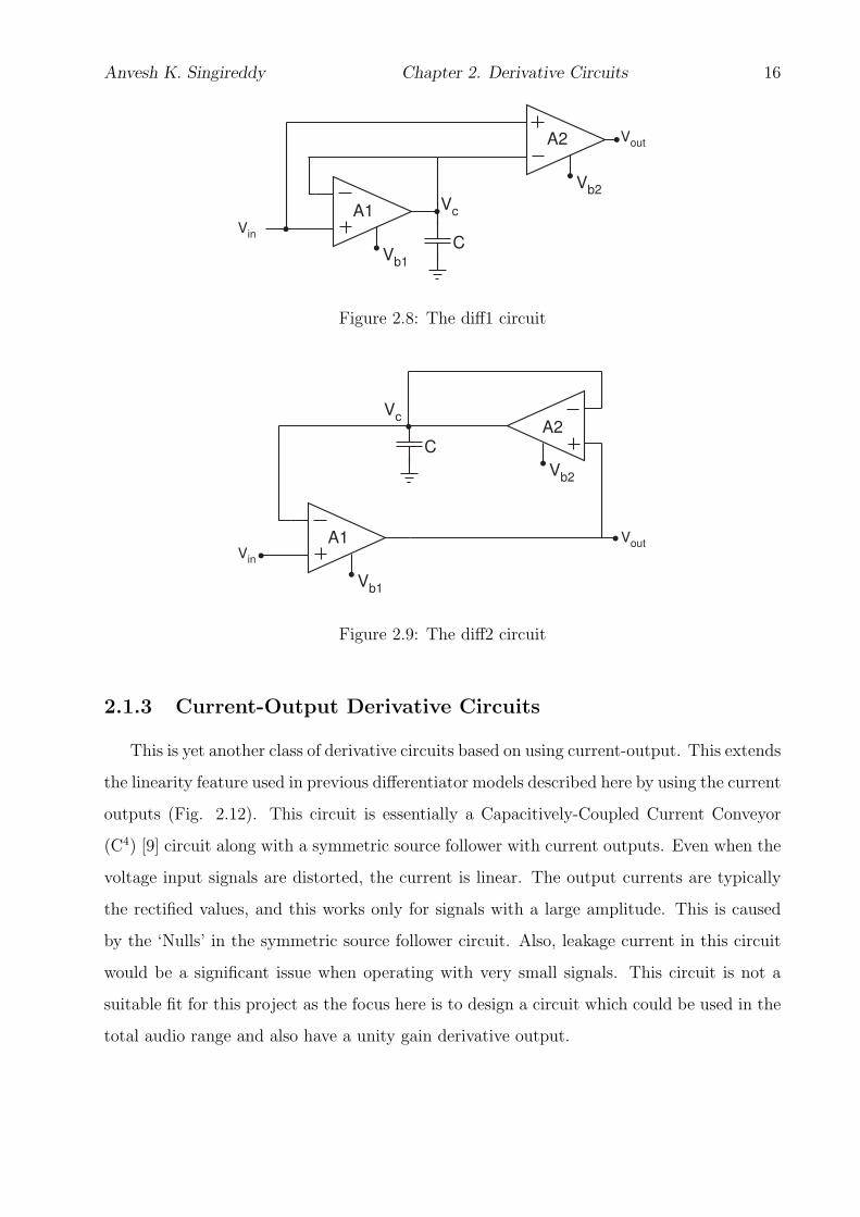
function as, Vout = A(Vin+−Vin−). This implementation is illustrated in 2.8 and is known as
Diff1 circuit [3]. But the problem with this circuit is that it has an open loop configuration
and even a small change in the offset voltage can lead to very high gain and clamp the output
at the supply rails.
A different model of the circuit based on the same concept is considered, which has
a negative feedback configuration. Also, this limits the huge changes in the output due
to mismatched offsets or mismatches caused during fabrication. This alternative circuit is
known as Diff2 (Fig. 2.9) [3]. In this circuit, the amplifier A2 (Fig. 2.9) is in a follower
configuration and its output is given to the negative input of the amplifier A1 (Fig. 2.9).
This performs the subtraction of the the time-averaged signal from the original version. The
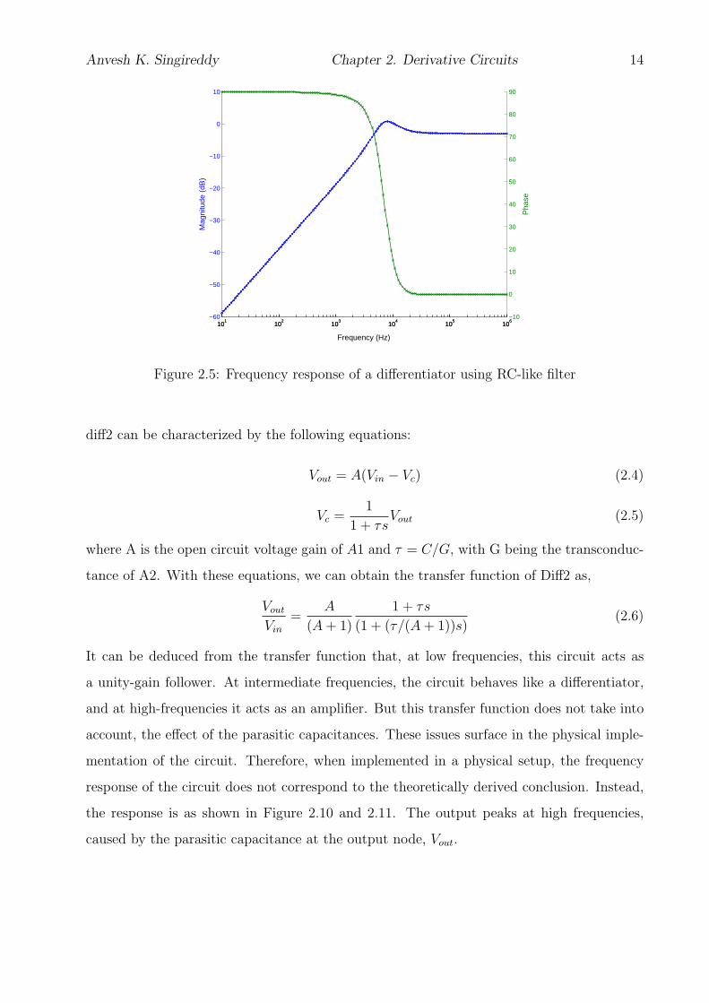
Anvesh K. Singireddy Chapter 2. Derivative Circuits 14
101
102
103
104
105
106
−60
−50
−40
−30
−20
−10
0
10
Mag
nitu
de (
dB)
101
102
103
104
105
106−10
0
10
20
30
40
50
60
70
80
90
Frequency (Hz)
Pha
se
Figure 2.5: Frequency response of a differentiator using RC-like filter
diff2 can be characterized by the following equations:
Vout = A(Vin − Vc) (2.4)
Vc =1
1 + τsVout (2.5)
where A is the open circuit voltage gain of A1 and τ = C/G, with G being the transconduc-
tance of A2. With these equations, we can obtain the transfer function of Diff2 as,
Vout
Vin
=A
(A + 1)
1 + τs
(1 + (τ/(A + 1))s)(2.6)
It can be deduced from the transfer function that, at low frequencies, this circuit acts as
a unity-gain follower. At intermediate frequencies, the circuit behaves like a differentiator,
and at high-frequencies it acts as an amplifier. But this transfer function does not take into
account, the effect of the parasitic capacitances. These issues surface in the physical imple-
mentation of the circuit. Therefore, when implemented in a physical setup, the frequency
response of the circuit does not correspond to the theoretically derived conclusion. Instead,
the response is as shown in Figure 2.10 and 2.11. The output peaks at high frequencies,
caused by the parasitic capacitance at the output node, Vout.
Anvesh K. Singireddy Chapter 2. Derivative Circuits 15
Vin
Vout
A
R
C Ic
VC
(a)
Vref
A
R
CIc
Vout
Vin
VC
(b)
Figure 2.6: Grounded Capacitor and Clamped capacitor approaches for differentiation
Vin
Vout
Vb
Figure 2.7: Follower integrator circuit. The bias voltage of the transconductance amplifiercan be used to modify the bias integrator’s time constant.
When this model is considered in the perspective of the requirements for the current
project, it does not fit in perfectly. First, it has the “differentiator slope” for a small range
of frequencies. It also has very high gain. Second, with a high gain, it would result in higher
THD as the higher harmonics would be amplified exponentially. Higher noise levels are also
observed in this circuit. Also, it causes clipping and distortion at high frequencies as the
high gain can cause the output to go rail-to-rail. Apart from all these factors, the output
might even oscillate due to high-frequency Q. Therefore, this model also is not suitable for
the required application.
Anvesh K. Singireddy Chapter 2. Derivative Circuits 16
Vin
Vout
Vb1
Vb2
C
A1
A2
Vc
Figure 2.8: The diff1 circuit
Vin
Vout
Vb1
Vb2
A2
A1
C
Vc
Figure 2.9: The diff2 circuit
2.1.3 Current-Output Derivative Circuits
This is yet another class of derivative circuits based on using current-output. This extends
the linearity feature used in previous differentiator models described here by using the current
outputs (Fig. 2.12). This circuit is essentially a Capacitively-Coupled Current Conveyor
(C4) [9] circuit along with a symmetric source follower with current outputs. Even when the
voltage input signals are distorted, the current is linear. The output currents are typically
the rectified values, and this works only for signals with a large amplitude. This is caused
by the ‘Nulls’ in the symmetric source follower circuit. Also, leakage current in this circuit
would be a significant issue when operating with very small signals. This circuit is not a
suitable fit for this project as the focus here is to design a circuit which could be used in the
total audio range and also have a unity gain derivative output.
Anvesh K. Singireddy Chapter 2. Derivative Circuits 17
101
102
103
104
105
106
−50
−40
−30
−20
−10
0
10
20
Mag
nitu
de (
dB)
101
102
103
104
105
106−350
−300
−250
−200
−150
−100
−50
0
Frequency (Hz)
Pha
se
Figure 2.10: Frequency response of diff2 (simulated)
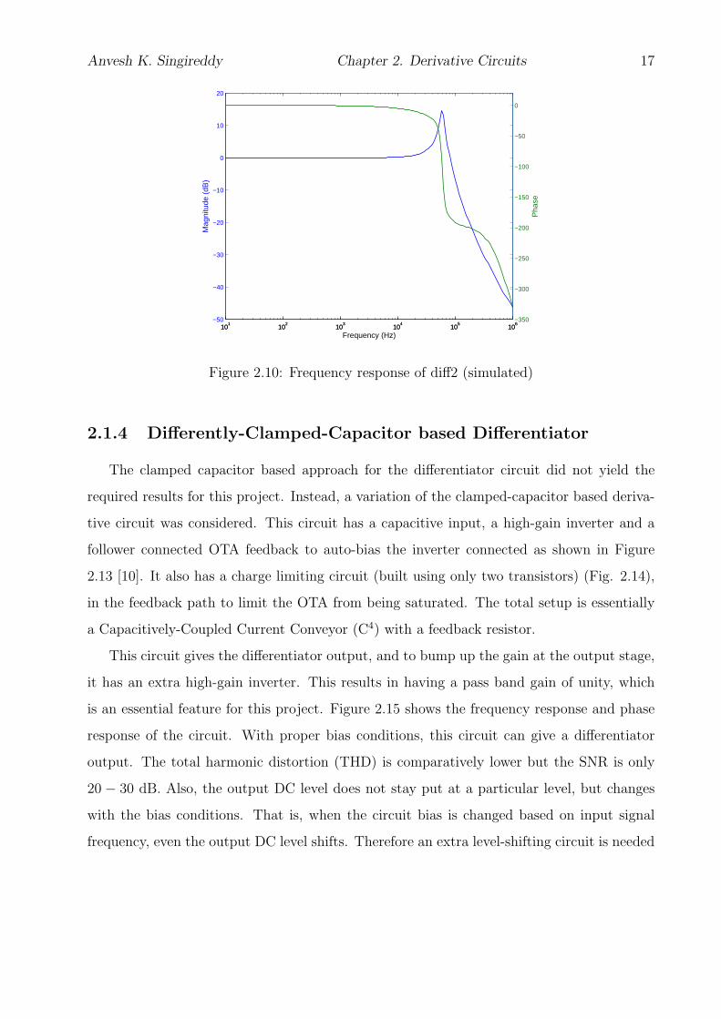
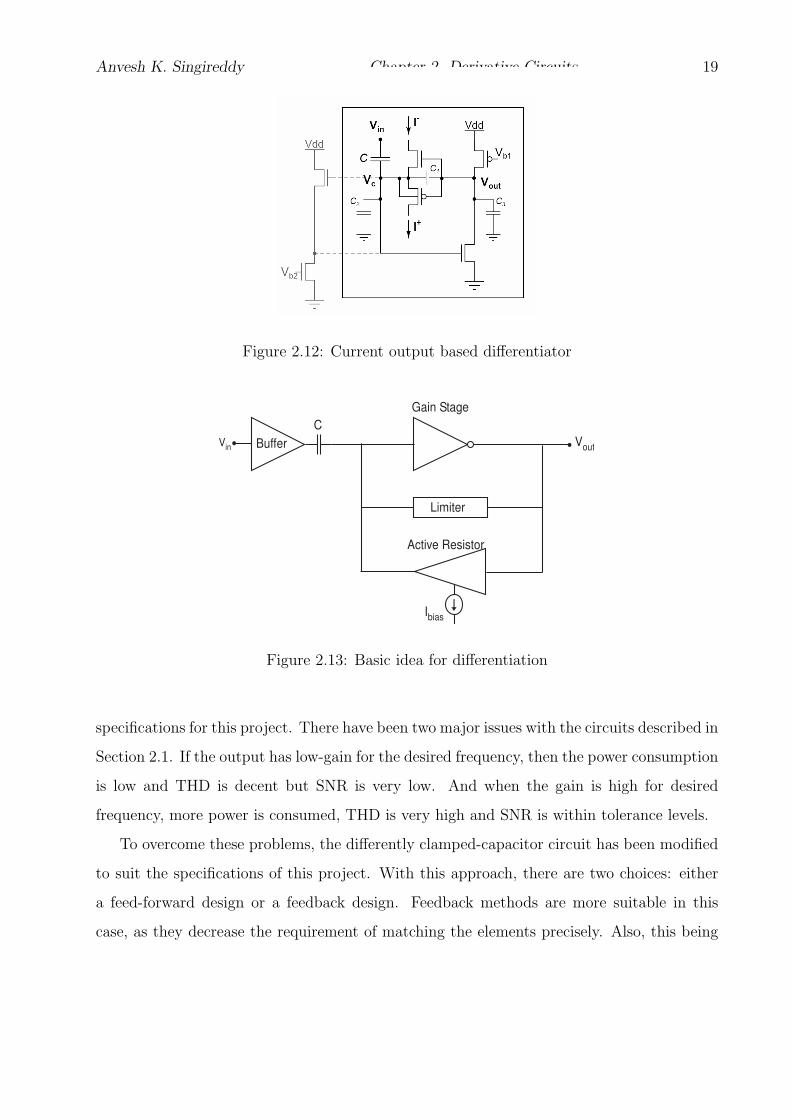
2.1.4 Differently-Clamped-Capacitor based Differentiator
The clamped capacitor based approach for the differentiator circuit did not yield the
required results for this project. Instead, a variation of the clamped-capacitor based deriva-
tive circuit was considered. This circuit has a capacitive input, a high-gain inverter and a
follower connected OTA feedback to auto-bias the inverter connected as shown in Figure
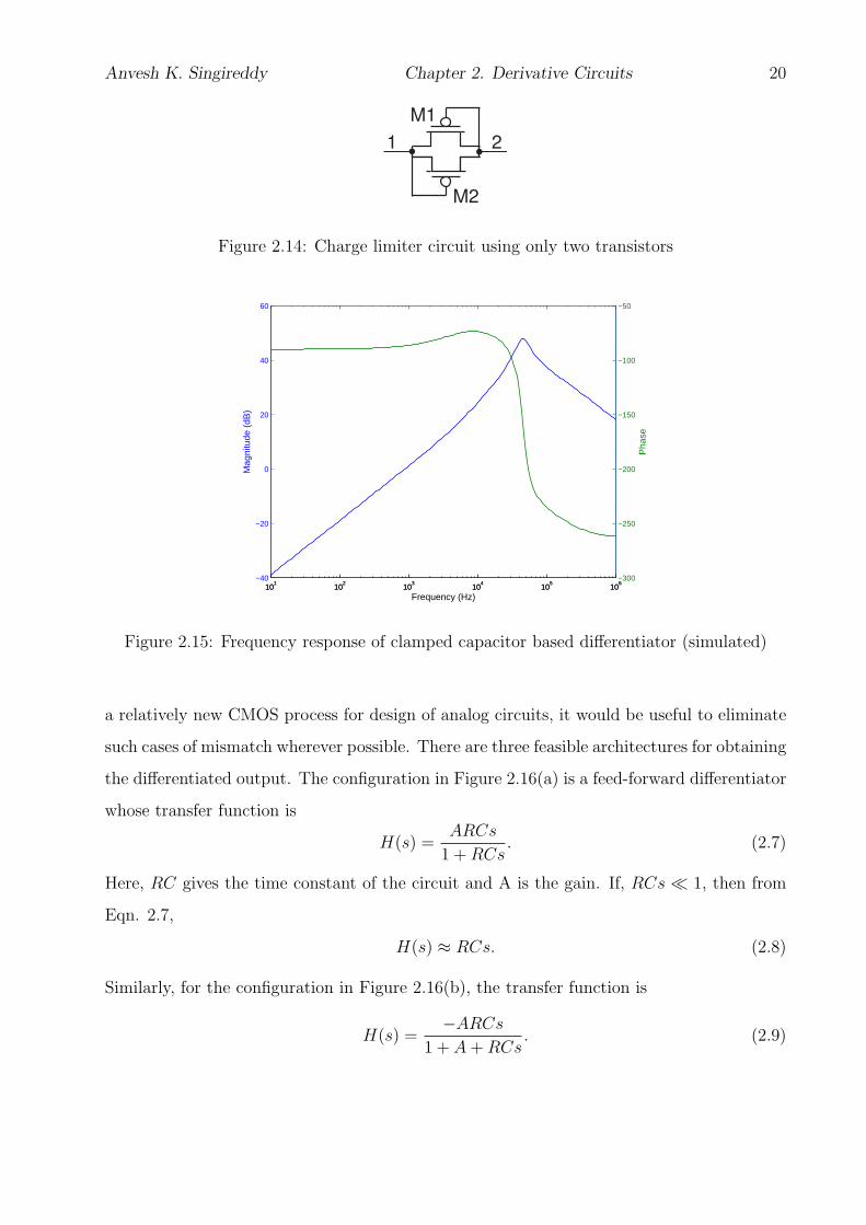
2.13 [10]. It also has a charge limiting circuit (built using only two transistors) (Fig. 2.14),
in the feedback path to limit the OTA from being saturated. The total setup is essentially
a Capacitively-Coupled Current Conveyor (C4) with a feedback resistor.
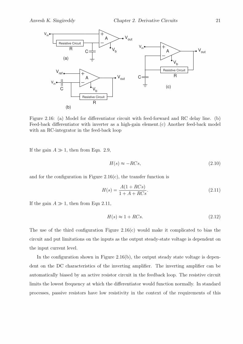
This circuit gives the differentiator output, and to bump up the gain at the output stage,
it has an extra high-gain inverter. This results in having a pass band gain of unity, which
is an essential feature for this project. Figure 2.15 shows the frequency response and phase
response of the circuit. With proper bias conditions, this circuit can give a differentiator
output. The total harmonic distortion (THD) is comparatively lower but the SNR is only
20 − 30 dB. Also, the output DC level does not stay put at a particular level, but changes
with the bias conditions. That is, when the circuit bias is changed based on input signal
frequency, even the output DC level shifts. Therefore an extra level-shifting circuit is needed
Anvesh K. Singireddy Chapter 2. Derivative Circuits 18
101
102
103
104
105
106
−80
−70
−60
−50
−40
−30
−20
−10
0
10
20
Frequency (Hz)
Mag
nitu
de (
dB)
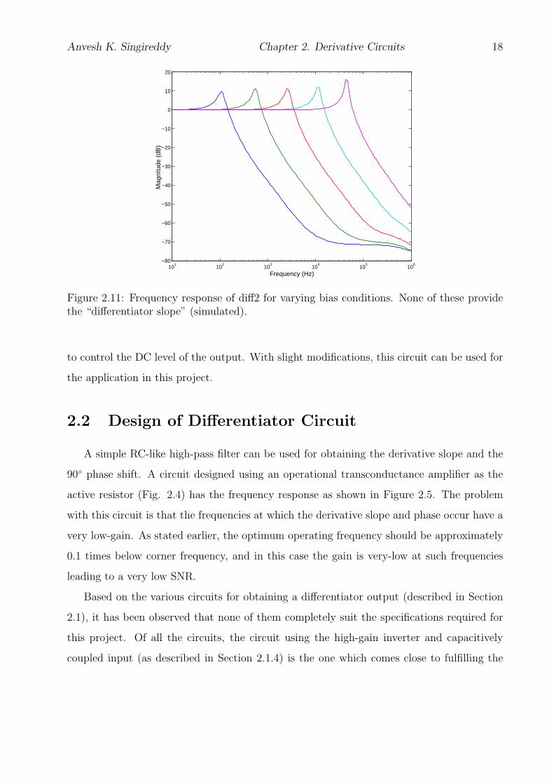
Figure 2.11: Frequency response of diff2 for varying bias conditions. None of these providethe “differentiator slope” (simulated).
to control the DC level of the output. With slight modifications, this circuit can be used for
the application in this project.
2.2 Design of Differentiator Circuit
A simple RC-like high-pass filter can be used for obtaining the derivative slope and the
90◦ phase shift. A circuit designed using an operational transconductance amplifier as the
active resistor (Fig. 2.4) has the frequency response as shown in Figure 2.5. The problem
with this circuit is that the frequencies at which the derivative slope and phase occur have a
very low-gain. As stated earlier, the optimum operating frequency should be approximately
0.1 times below corner frequency, and in this case the gain is very-low at such frequencies
leading to a very low SNR.
Based on the various circuits for obtaining a differentiator output (described in Section
2.1), it has been observed that none of them completely suit the specifications required for
this project. Of all the circuits, the circuit using the high-gain inverter and capacitively
coupled input (as described in Section 2.1.4) is the one which comes close to fulfilling the
Anvesh K. Singireddy Chapter 2. Derivative Circuits 19
Figure 2.12: Current output based differentiator
C
BufferVin Vout
Gain Stage
Limiter
Active Resistor
Ibias
Figure 2.13: Basic idea for differentiation
specifications for this project. There have been two major issues with the circuits described in
Section 2.1. If the output has low-gain for the desired frequency, then the power consumption
is low and THD is decent but SNR is very low. And when the gain is high for desired
frequency, more power is consumed, THD is very high and SNR is within tolerance levels.
To overcome these problems, the differently clamped-capacitor circuit has been modified
to suit the specifications of this project. With this approach, there are two choices: either
a feed-forward design or a feedback design. Feedback methods are more suitable in this
case, as they decrease the requirement of matching the elements precisely. Also, this being
Anvesh K. Singireddy Chapter 2. Derivative Circuits 20
1 2
M1
M2
Figure 2.14: Charge limiter circuit using only two transistors
101
102
103
104
105
106
−40
−20
0
20
40
60
Mag
nitu
de (
dB)
101
102
103
104
105
106−300
−250
−200
−150
−100
−50
Frequency (Hz)
Pha
seFigure 2.15: Frequency response of clamped capacitor based differentiator (simulated)
a relatively new CMOS process for design of analog circuits, it would be useful to eliminate
such cases of mismatch wherever possible. There are three feasible architectures for obtaining
the differentiated output. The configuration in Figure 2.16(a) is a feed-forward differentiator
whose transfer function is
H(s) =ARCs
1 + RCs. (2.7)
Here, RC gives the time constant of the circuit and A is the gain. If, RCs � 1, then from
Eqn. 2.7,
H(s) ≈ RCs. (2.8)
Similarly, for the configuration in Figure 2.16(b), the transfer function is
H(s) =−ARCs
1 + A + RCs. (2.9)
Anvesh K. Singireddy Chapter 2. Derivative Circuits 21
VbC
Vout
Vin
Resistive Circuit
A
R
C
Vb
Vout
Vin
Resistive Circuit
R
A
Vin
C Vb
Vout
Resistive Circuit
R
A
Vref
(a)
(b)
(c)
Figure 2.16: (a) Model for differentiator circuit with feed-forward and RC delay line. (b)Feed-back differentiator with inverter as a high-gain element.(c) Another feed-back modelwith an RC-integrator in the feed-back loop
If the gain A � 1, then from Eqn. 2.9,
H(s) ≈ −RCs, (2.10)
and for the configuration in Figure 2.16(c), the transfer function is
H(s) =A(1 + RCs)
1 + A + RCs. (2.11)
If the gain A � 1, then from Eqn 2.11,
H(s) ≈ 1 + RCs. (2.12)
The use of the third configuration Figure 2.16(c) would make it complicated to bias the
circuit and put limitations on the inputs as the output steady-state voltage is dependent on
the input current level.
In the configuration shown in Figure 2.16(b), the output steady state voltage is depen-
dent on the DC characteristics of the inverting amplifier. The inverting amplifier can be
automatically biased by an active resistor circuit in the feedback loop. The resistive circuit
limits the lowest frequency at which the differentiator would function normally. In standard
processes, passive resistors have low resistivity in the context of the requirements of this
Anvesh K. Singireddy Chapter 2. Derivative Circuits 22
Vbias
Vin
Vout
M1
M2
M3
M4
M5
M6
M7
M8
Figure 2.17: The basic differentiator circuit
circuit. The active resistors can be designed using a modified version of an Operational
Transconductance Amplifier (OTA). The active resistor may go into saturation if the charge
is too high and result in non-ideal output. Therefore, a limiting circuit is used to limit the
charge on the active resistor and preventing it from saturating. The limiting circuit can
inject a large amount of charge onto the output node of the active resistor. The amount of
charge injected depends on the limiting circuit. This way, a differentiator circuit can be de-
signed to meet the specific requirements of this project. The following sub-section describes
each block of this circuit.
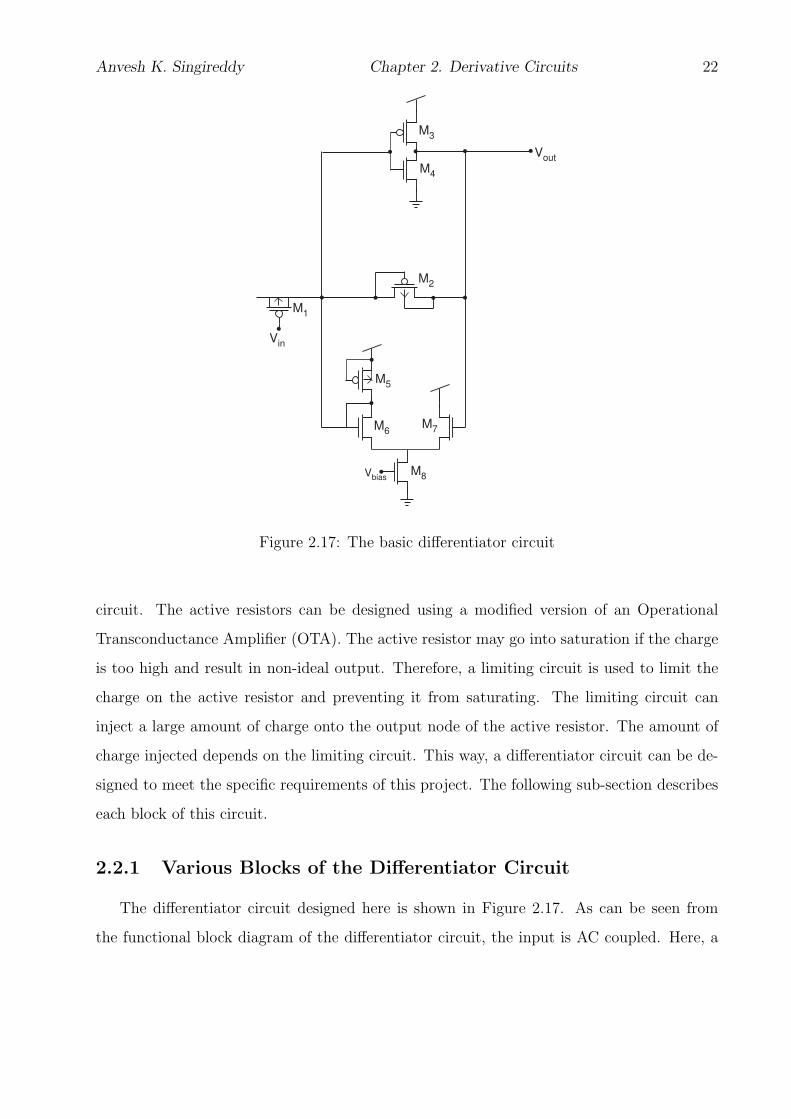
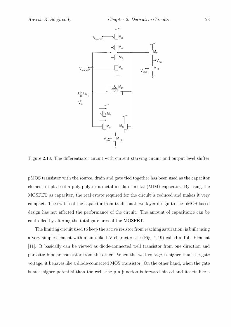
2.2.1 Various Blocks of the Differentiator Circuit
The differentiator circuit designed here is shown in Figure 2.17. As can be seen from
the functional block diagram of the differentiator circuit, the input is AC coupled. Here, a
Anvesh K. Singireddy Chapter 2. Derivative Circuits 23
Vbias
Vstarve1
Vin
Vshift
Vout
M1
M2
M3
M4
M5
M6
M11
M12
M7
M8
M9
M10
Vstarve2
Figure 2.18: The differentiator circuit with current starving circuit and output level shifter
pMOS transistor with the source, drain and gate tied together has been used as the capacitor
element in place of a poly-poly or a metal-insulator-metal (MIM) capacitor. By using the
MOSFET as capacitor, the real estate required for the circuit is reduced and makes it very
compact. The switch of the capacitor from traditional two layer design to the pMOS based
design has not affected the performance of the circuit. The amount of capacitance can be
controlled by altering the total gate area of the MOSFET.
The limiting circuit used to keep the active resistor from reaching saturation, is built using
a very simple element with a sinh-like I-V characteristic (Fig. 2.19) called a Tobi Element
[11]. It basically can be viewed as diode-connected well transistor from one direction and
parasitic bipolar transistor from the other. When the well voltage is higher than the gate
voltage, it behaves like a diode-connected MOS transistor. On the other hand, when the gate
is at a higher potential than the well, the p-n junction is forward biased and it acts like a
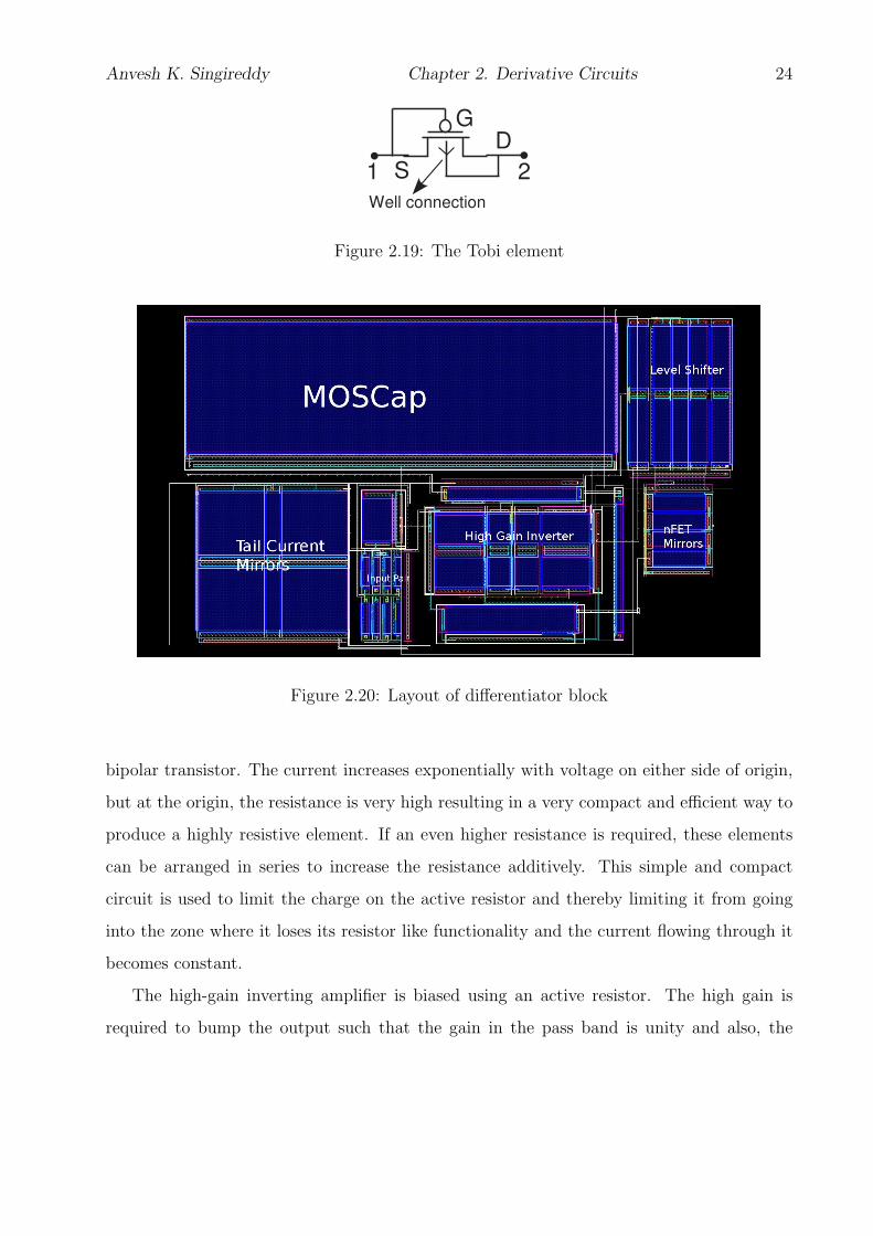
Anvesh K. Singireddy Chapter 2. Derivative Circuits 24
1 2
G
S
D
Well connection
Figure 2.19: The Tobi element
Figure 2.20: Layout of differentiator block
bipolar transistor. The current increases exponentially with voltage on either side of origin,
but at the origin, the resistance is very high resulting in a very compact and efficient way to
produce a highly resistive element. If an even higher resistance is required, these elements
can be arranged in series to increase the resistance additively. This simple and compact
circuit is used to limit the charge on the active resistor and thereby limiting it from going
into the zone where it loses its resistor like functionality and the current flowing through it
becomes constant.
The high-gain inverting amplifier is biased using an active resistor. The high gain is
required to bump the output such that the gain in the pass band is unity and also, the

Anvesh K. Singireddy Chapter 2. Derivative Circuits 25
“differentiation phase” of 90◦ is achieved. Also, the current to the inverter is limited using a
current-starving configuration as can be seen in (Fig. 2.18). This is done to have control on
the amount of current to the inverter, thereby providing control over the total power con-
sumption of the inverter. In general, the inverter is a comparatively high-power-consumption
circuit. In this way, the circuit could be tuned to function in low-power consumption mode
and at normal performance. This performance trade-off is due to the lower gain on the out-
put resulting in the total shift of frequency response, resulting in a lower gain than unity for
the output. This in turn results in loss of the perfect 90◦ phase difference between the input
and output. In a few applications which require only the temporal change patterns, such
small loss can be tolerated for lowering power consumption. And for situations where the
phase and gain have to be precise, a high power mode can be used. By tuning the circuit such
that the inverter can operate freely without limiting the current through it, the total power
consumption increases but the desired performance can be achieved. The active resistor is
designed based on a diff-pair. This active resistor sets the operating bias conditions for the
inverting amplifier. The bias on this circuit is used to tune the differentiator for operation
in different pass-bands.
For differentiating signals of different frequencies the bias conditions need to be varied.
The output steady-state voltage of the derivative circuit varies with bias conditions. This
change in the steady-state output voltage is due to varying bias conditions of the inverting
amplifier, and thus, resulting in a different DC level of the output for each frequency range.
To tie the output DC level at a constant level, an extra level-shifter circuit is added at the
output stage (Fig. 2.18) of the basic differentiator circuit. This circuit has its own bias
and can be tuned to shift the steady state value of the output as per the requirements of a
particular application. The layout of the differentiator block is shown in Figure 2.20 and it
measures 51µm by 84µm.
2.2.2 Results from the Differentiator Circuit
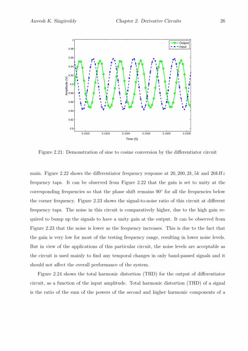
Figure 2.21 shows the basic operation of the differentiator circuit for a sinusoidal input:
a sinusoidal input is shifted in phase by 90◦ to get its differentiated output in time do-
Anvesh K. Singireddy Chapter 2. Derivative Circuits 26
0.1503 0.1503 0.1504 0.1505 0.1505 0.1505
0.8
0.82
0.84
0.86
0.88
0.9
0.92
0.94
0.96
0.98
1
Time (S)
Am
plitu
de (
V)
OutputInput
Figure 2.21: Demonstration of sine to cosine conversion by the differentiator circuit
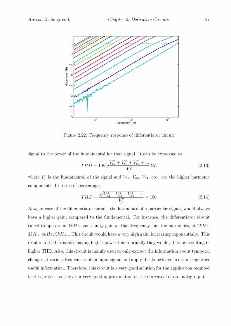
main. Figure 2.22 shows the differentiator frequency response at 20, 200, 2k, 5k and 20kHz
frequency taps. It can be observed from Figure 2.22 that the gain is set to unity at the
corresponding frequencies so that the phase shift remains 90◦ for all the frequencies below
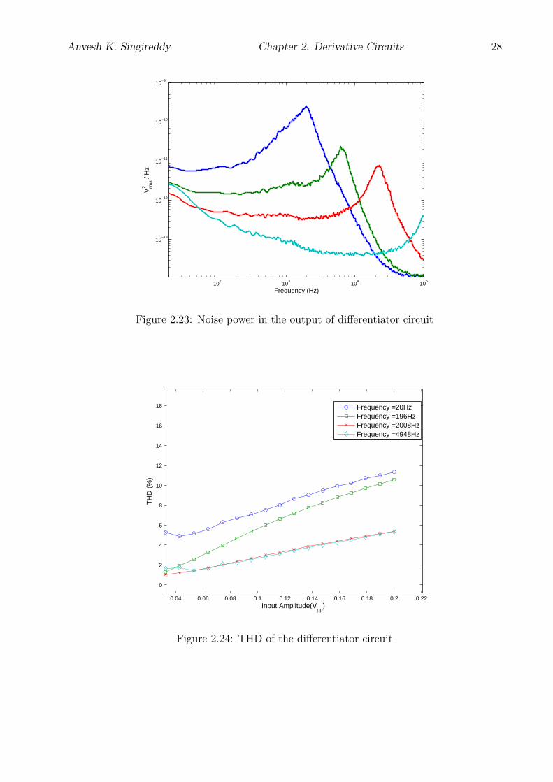
the corner frequency. Figure 2.23 shows the signal-to-noise ratio of this circuit at different
frequency taps. The noise in this circuit is comparatively higher, due to the high gain re-
quired to bump up the signals to have a unity gain at the output. It can be observed from
Figure 2.23 that the noise is lower as the frequency increases. This is due to the fact that
the gain is very low for most of the testing frequency range, resulting in lower noise levels.
But in view of the applications of this particular circuit, the noise levels are acceptable as
the circuit is used mainly to find any temporal changes in only band-passed signals and it
should not affect the overall performance of the system.
Figure 2.24 shows the total harmonic distortion (THD) for the output of differentiator
circuit, as a function of the input amplitude. Total harmonic distortion (THD) of a signal
is the ratio of the sum of the powers of the second and higher harmonic components of a
Anvesh K. Singireddy Chapter 2. Derivative Circuits 27
102
103
104
−70
−60
−50
−40
−30
−20
−10
0
Frequency (Hz)
Mag
nitu
de (
dB)
Figure 2.22: Frequency response of differentiator circuit
signal to the power of the fundamental for that signal. It can be expressed as,
THD = 10logV 2
h2 + V 2h3 + V 2
h4 + ...
V 2f
dB, (2.13)
where Vf is the fundamental of the signal and Vh2, Vh3, Vh4, etc. are the higher harmonic
components. In terms of percentage,
THD =
√V 2
h2 + V 2h3 + V 2
h4 + ...
V 2f
× 100 (2.14)
Now, in case of the differentiator circuit, the harmonics of a particular signal, would always
have a higher gain, compared to the fundamental. For instance, the differentiator circuit
tuned to operate at 1kHz has a unity gain at that frequency, but the harmonics, at 2kHz,
3kHz, 4kHz, 5kHz,...This circuit would have a very high gain, increasing exponentially. This
results in the harmonics having higher power than normally they would, thereby resulting in
higher THD. Also, this circuit is mainly used to only extract the information about temporal
changes at various frequencies of an input signal and apply this knowledge in extracting other
useful information. Therefore, this circuit is a very good solution for the application required
in this project as it gives a very good approximation of the derivative of an analog input.
Anvesh K. Singireddy Chapter 2. Derivative Circuits 28
102
103
104
105
10−13
10−12
10−11
10−10
10−9
V2 rm
s / H
z
Frequency (Hz)
Figure 2.23: Noise power in the output of differentiator circuit
0.04 0.06 0.08 0.1 0.12 0.14 0.16 0.18 0.2 0.22
0
2
4
6
8
10
12
14
16
18
Input Amplitude(Vpp
)
TH
D (
%)
Frequency =20HzFrequency =196HzFrequency =2008HzFrequency =4948Hz
Figure 2.24: THD of the differentiator circuit
29
Chapter 3
Subtractor Circuit
In general, voltage-mode adders and subtractors form a very essential part of collective
analog computational systems [12]. To perform a few application specific tasks on the sub-
banded signals, a voltage-mode subtractor circuit is required. In this project, analog signals
are first spectrally decomposed, and then various signal processing algorithms are applied
on them to extract the required information. These processed signals are then sent to the
analog-to-digital converter and then to the digital signal processor for further processing.
The first phase of processing is done using the analog front-end designed in this project. As
part of this front-end, a voltage-mode subtractor is designed.
The subtractor circuit designed here is for low-power consumption and high-dynamic
range. The power consumption is in µWs and the dynamic range is 64dB. Also, the circuit
is very easily tuned as it works over the whole audio range using only one bias value; that
is, it does not need a seperate bias for each single tap in the larger system. This chapter
describes the design and operation of the subtractor circuit.
3.1 Basic Principle
As current can be easily added or subtracted based on Kirchoff’s current law, a voltage-
mode subtractor circuit could be designed by first converting voltage signals into current
and then converting them back to voltage after the required operation has been done. This
conversion can be done using an operational transconductance amplifier (OTA) or current
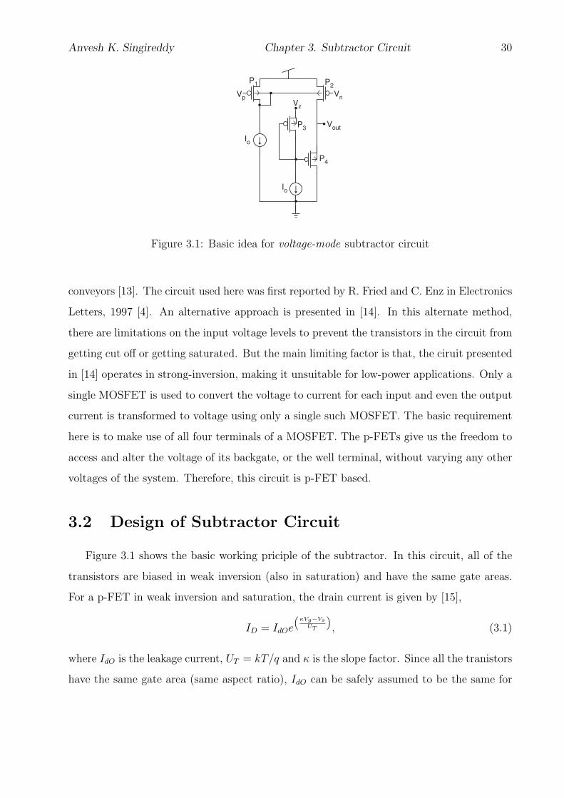
Anvesh K. Singireddy Chapter 3. Subtractor Circuit 30
Vp Vn
Vout
Vz
Io
Io
P1 P2
P3
P4
Figure 3.1: Basic idea for voltage-mode subtractor circuit
conveyors [13]. The circuit used here was first reported by R. Fried and C. Enz in Electronics
Letters, 1997 [4]. An alternative approach is presented in [14]. In this alternate method,
there are limitations on the input voltage levels to prevent the transistors in the circuit from
getting cut off or getting saturated. But the main limiting factor is that, the ciruit presented
in [14] operates in strong-inversion, making it unsuitable for low-power applications. Only a
single MOSFET is used to convert the voltage to current for each input and even the output
current is transformed to voltage using only a single such MOSFET. The basic requirement
here is to make use of all four terminals of a MOSFET. The p-FETs give us the freedom to
access and alter the voltage of its backgate, or the well terminal, without varying any other
voltages of the system. Therefore, this circuit is p-FET based.
3.2 Design of Subtractor Circuit
Figure 3.1 shows the basic working priciple of the subtractor. In this circuit, all of the
transistors are biased in weak inversion (also in saturation) and have the same gate areas.
For a p-FET in weak inversion and saturation, the drain current is given by [15],
ID = IdOe
“
κVg−VsUT
”
, (3.1)
where IdO is the leakage current, UT = kT/q and κ is the slope factor. Since all the tranistors
have the same gate area (same aspect ratio), IdO can be safely assumed to be the same for
Anvesh K. Singireddy Chapter 3. Subtractor Circuit 31
all the transistors. This gives the relation between the bias current and output as,
Iout
Ibias
= e
“
κ(Vp−Vn)
UT
”
. (3.2)
From equations 3.1 and 3.2, the voltage at the output transistor, P4 (Fig. 3.1) is given by,
Vout = Vp − Vn +
(κ
UT
)ln
(Ibias
IdO
)+ Vg, (3.3)
where Vp and Vn are the input voltages and Vg is the gate voltage of P3 (Fig. 3.1). The
equation 3.3 clearly shows that the output voltage is the difference of the two input voltages
along with a small offset voltage Voff−set, which is given by,
Voff−set =
(κ
UT
)ln
(Ibias
IdO
)+ Vg. (3.4)
The gate voltage of the transistor P3 (Fig. 3.1) is given by,
Vg = Vz −(
κ
UT
)ln
(Ibias
IdO
). (3.5)
Now, from equations 3.3, 3.4 and 3.5,
Vout = Vp − Vn + Vz. (3.6)
This gives us the required subtractor operation. The extra offset voltage, Vz can be used to
set a constant offset voltage for the output or can even be used as additional input voltage.
Therefore, this circuit has the potential to be used as either a subtractor or as an adder.
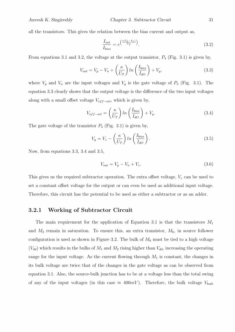
3.2.1 Working of Subtractor Circuit
The main requirement for the application of Equation 3.1 is that the transistors M1
and M2 remain in saturation. To ensure this, an extra transistor, M6, in source follower
configuration is used as shown in Figure 3.2. The bulk of M6 must be tied to a high voltage
(Vdd) which results in the bulks of M1 and M2 rising higher than Vdd, increasing the operating
range for the input voltage. As the current flowing through M1 is constant, the changes in
its bulk voltage are twice that of the changes in the gate voltage as can be observed from
equation 3.1. Also, the source-bulk junction has to be at a voltage less than the total swing
of any of the input voltages (in this case ≈ 400mV ). Therefore, the bulk voltage Vbulk
Anvesh K. Singireddy Chapter 3. Subtractor Circuit 32
Vp Vn
Vout
Vz
Vbias
M1
M5 M6
M7
M2
M4
M3
M10M9M8
Vg
Figure 3.2: Subtractor circuit
needs to be greater than the sum of VThreshold, the maximum input swing and VDsat (that
is, Vbulk ≥ VThreshold + VDsat + 400mV ) . For this reason, the bulk can be tied safely to Vdd.
This also eliminates the need of an extra biasing input.
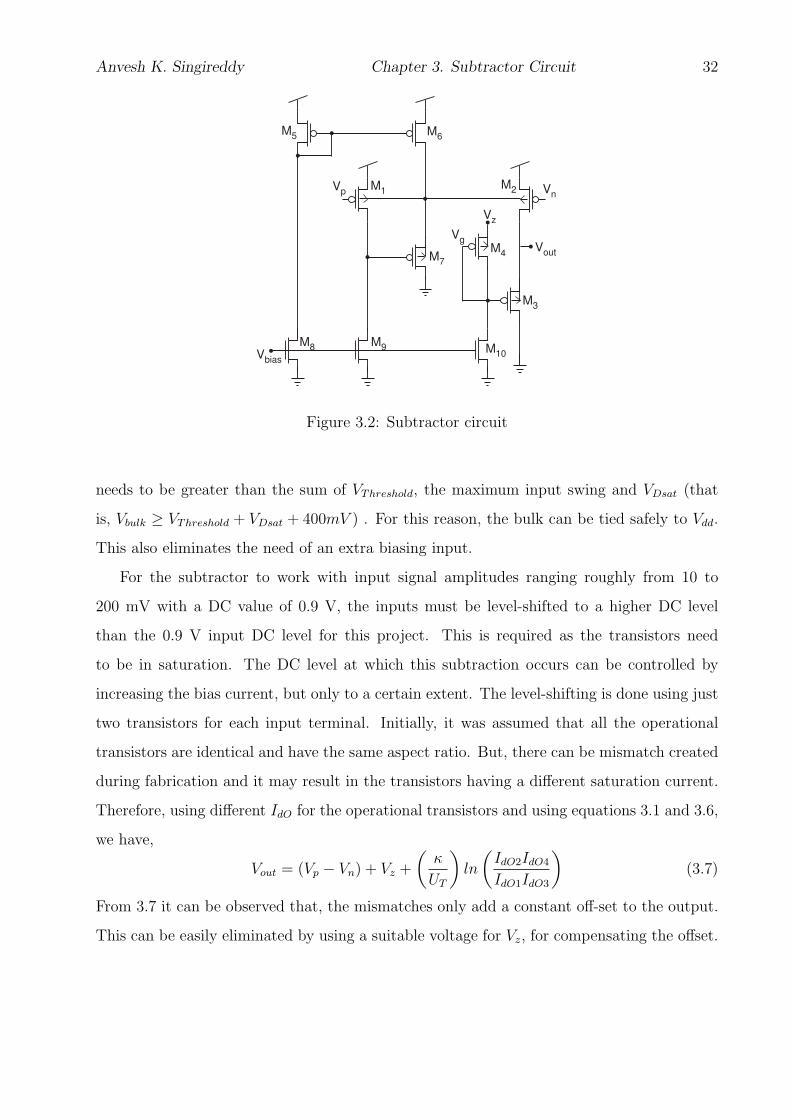
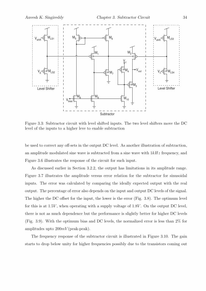
For the subtractor to work with input signal amplitudes ranging roughly from 10 to
200 mV with a DC value of 0.9 V, the inputs must be level-shifted to a higher DC level
than the 0.9 V input DC level for this project. This is required as the transistors need
to be in saturation. The DC level at which this subtraction occurs can be controlled by
increasing the bias current, but only to a certain extent. The level-shifting is done using just
two transistors for each input terminal. Initially, it was assumed that all the operational
transistors are identical and have the same aspect ratio. But, there can be mismatch created
during fabrication and it may result in the transistors having a different saturation current.
Therefore, using different IdO for the operational transistors and using equations 3.1 and 3.6,
we have,
Vout = (Vp − Vn) + Vz +
(κ
UT
)ln
(IdO2IdO4
IdO1IdO3
)(3.7)
From 3.7 it can be observed that, the mismatches only add a constant off-set to the output.
This can be easily eliminated by using a suitable voltage for Vz, for compensating the offset.
Anvesh K. Singireddy Chapter 3. Subtractor Circuit 33
Moreover, this circuit requires only one bias voltage for its operation. With a single bias
value, it can perform the subtraction over the whole audio range without any requirement of
tuning for different frequencies. Also, as the operational transistors are identical, any changes
in circuit conditions due to temperature are automatically offset due to the symmetrical
nature of the circuit. The noise is level is lower in this circuit as most of it gets cancelled
out during the subtraction.
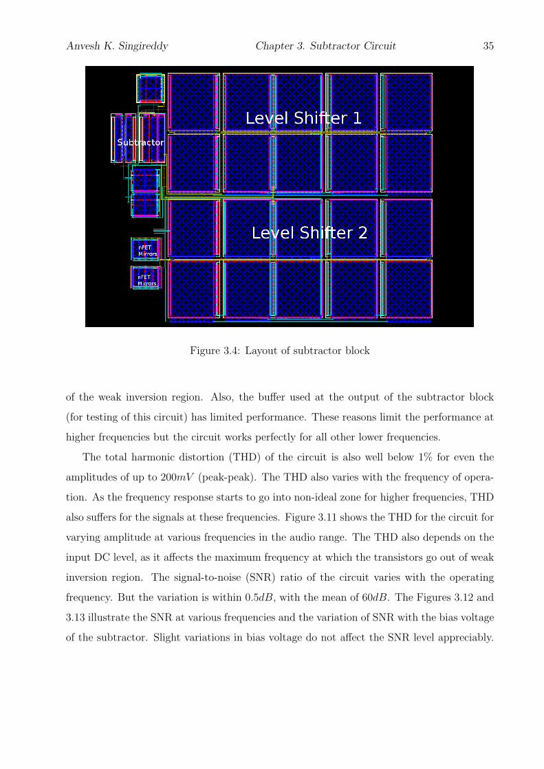
The layout of the subtractor block is shown in Figure 3.4 and it measures 115µm by
147µm. As can be observed from Figure 3.4, the core subtractor circuit is very small and
the maximum area is used up by the level shifters.
3.2.2 Output Limitations
The slope factor of the transistors changes with the change in gate-to-bulk voltage. The
upper and lower limit of the differential input voltage is therefore limited. The uppper limit
depends on the lower voltage of the bulks of M1 and M2 at which the source-bulk junction
is forward biased. The lower limit depends on the M1 tansistor’s gate voltage, beyond which
the transistor comes out of the weak inversion region. Even with these limits, the required
operational range is not much affected, as most of the singals are within 50− 200mV . Also,
its operating frequency is limited due to the use of MOSFETs in weak inversion. However,
it works reliably in the region below the upper end of the audio frequency range.
3.3 Results
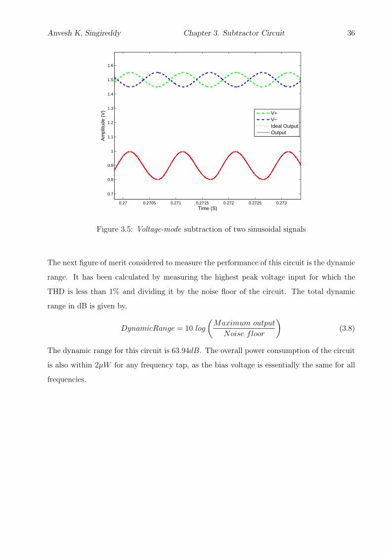
The Figure 3.3 shows the complete implementation of the subtractor circuit. To test the
basic operation of the circuit, a sine wave with an amplitude of 100mV and 1kHz frequency
is given as the input to the positive terminal. To the negative terminal, a similar input
with a phase shift of 180◦ (relative to the input at positive terminal) is given. Figure 3.5
illustrates the output of the circuit in this scenario. As can be observed in Figure 3.5, the
input DC level is shifted to 1.5V (from the 0.9V input DC level for this project) for the
saturation of the operational transistors and thereby facilitating subtraction. The output
DC level is set by the voltage Vz, which acts like an additional input to the circuit. This can
Anvesh K. Singireddy Chapter 3. Subtractor Circuit 34
Vshift
Vp
MLS1
MLS2Vout
Vz
Vbias
M1
M5 M6
M7
M2
M4
M3
M10M9M8
Vn
VshiftMLS3
MLS4
Subtractor
Level ShifterLevel Shifter
Figure 3.3: Subtractor circuit with level shifted inputs. The two level shifters move the DClevel of the inputs to a higher leve to enable subtraction
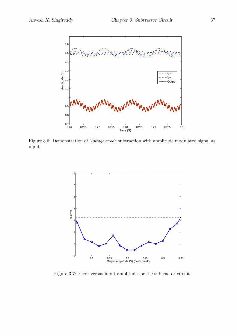
be used to correct any off-sets in the output DC level. As another illustration of subtraction,
an amplitude modulated sine wave is subtracted from a sine wave with 1kHz frequency, and
Figure 3.6 illustrates the response of the circuit for such input.
As discussed earlier in Section 3.2.2, the output has limitations in its amplitude range.
Figure 3.7 illustrates the amplitude versus error relation for the subtractor for sinusoidal
inputs. The error was calculated by comparing the ideally expected output with the real
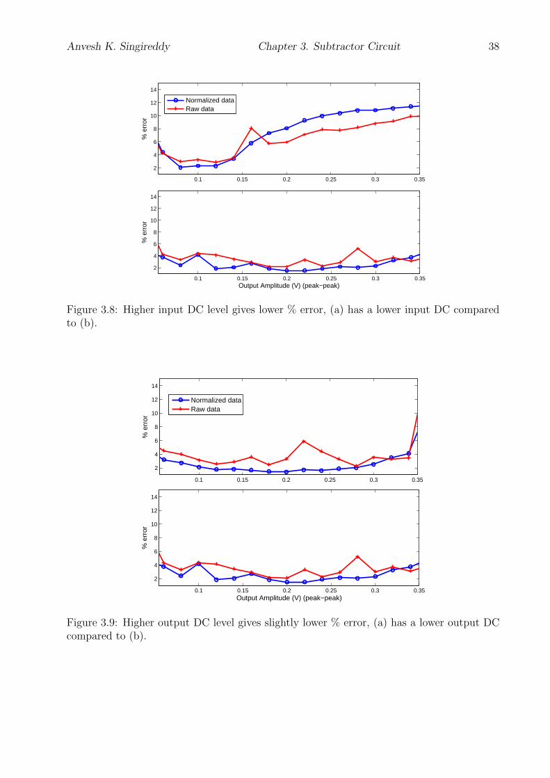
output. The percentage of error also depends on the input and output DC levels of the signal.
The higher the DC offset for the input, the lower is the error (Fig. 3.8). The optimum level
for this is at 1.5V , when operating with a supply voltage of 1.8V . On the output DC level,
there is not as much dependence but the performance is slightly better for higher DC levels
(Fig. 3.9). With the optimum bias and DC levels, the normalized error is less than 2% for
amplitudes upto 200mV (peak-peak).
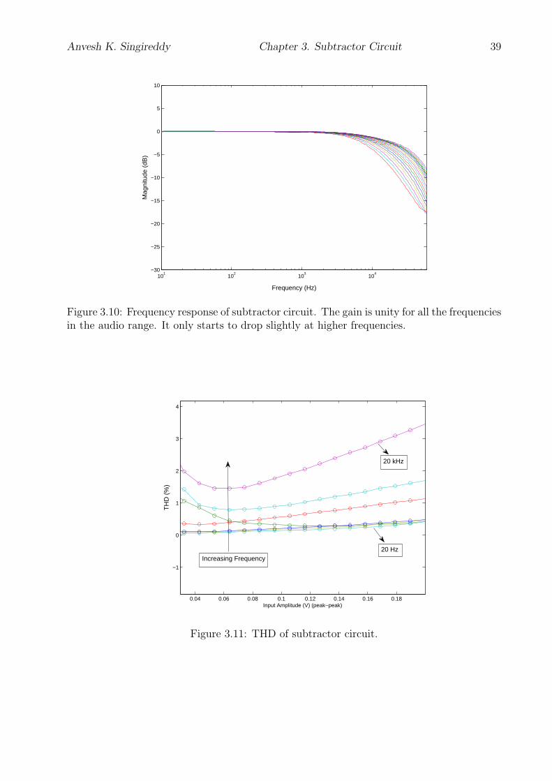
The frequency response of the subtractor circuit is illustrated in Figure 3.10. The gain
starts to drop below unity for higher frequencies possibly due to the transistors coming out
Anvesh K. Singireddy Chapter 3. Subtractor Circuit 35
Figure 3.4: Layout of subtractor block
of the weak inversion region. Also, the buffer used at the output of the subtractor block
(for testing of this circuit) has limited performance. These reasons limit the performance at
higher frequencies but the circuit works perfectly for all other lower frequencies.
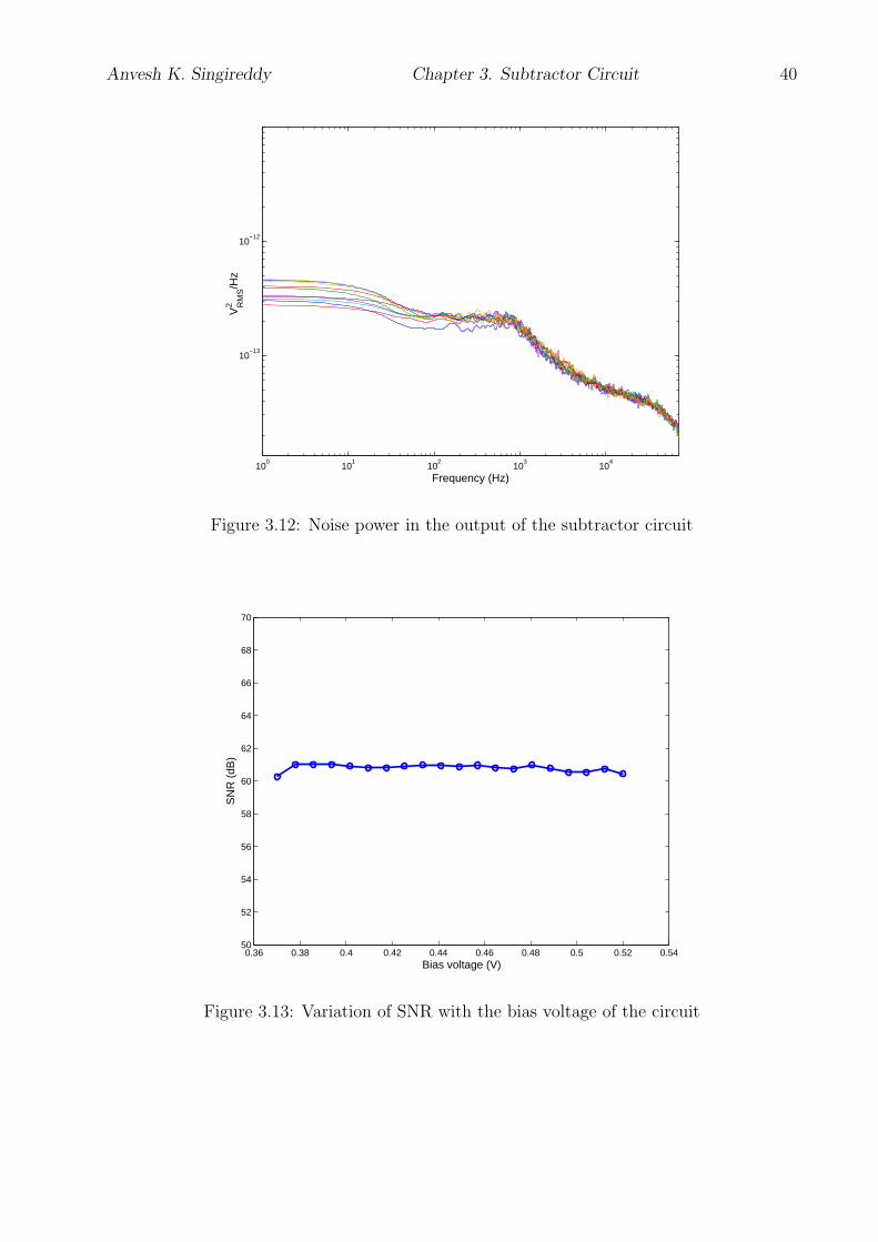
The total harmonic distortion (THD) of the circuit is also well below 1% for even the
amplitudes of up to 200mV (peak-peak). The THD also varies with the frequency of opera-
tion. As the frequency response starts to go into non-ideal zone for higher frequencies, THD
also suffers for the signals at these frequencies. Figure 3.11 shows the THD for the circuit for
varying amplitude at various frequencies in the audio range. The THD also depends on the
input DC level, as it affects the maximum frequency at which the transistors go out of weak
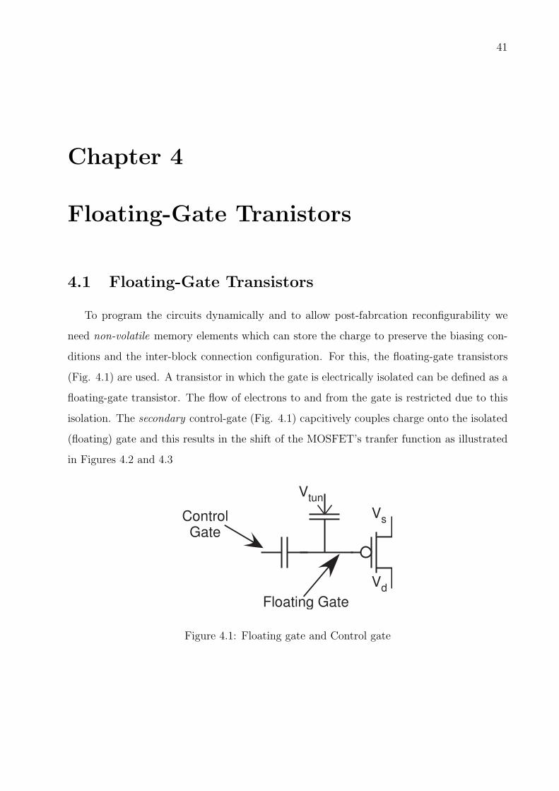
inversion region. The signal-to-noise (SNR) ratio of the circuit varies with the operating
frequency. But the variation is within 0.5dB, with the mean of 60dB. The Figures 3.12 and
3.13 illustrate the SNR at various frequencies and the variation of SNR with the bias voltage
of the subtractor. Slight variations in bias voltage do not affect the SNR level appreciably.
Anvesh K. Singireddy Chapter 3. Subtractor Circuit 36
0.27 0.2705 0.271 0.2715 0.272 0.2725 0.273
0.7
0.8
0.9
1
1.1
1.2
1.3
1.4
1.5
1.6
Time (S)
Am
plitu
de (
V)
V+V−Ideal OutputOutput
Figure 3.5: Voltage-mode subtraction of two sinusoidal signals
The next figure of merit considered to measure the performance of this circuit is the dynamic
range. It has been calculated by measuring the highest peak voltage input for which the
THD is less than 1% and dividing it by the noise floor of the circuit. The total dynamic
range in dB is given by,
DynamicRange = 10 log
(Maximum output
Noise floor
)(3.8)
The dynamic range for this circuit is 63.94dB. The overall power consumption of the circuit
is also within 2µW for any frequency tap, as the bias voltage is essentially the same for all
frequencies.
Anvesh K. Singireddy Chapter 3. Subtractor Circuit 37
0.26 0.265 0.27 0.275 0.28 0.285 0.29 0.295 0.30.7
0.8
0.9
1
1.1
1.2
1.3
1.4
1.5
1.6
Time (S)
Am
plitu
de (
V)
V+V−Output
Figure 3.6: Demonstration of Voltage-mode subtraction with amplitude modulated signal asinput.
0.1 0.15 0.2 0.25 0.3 0.351
2
3
4
5
6
7
8
Output amplitude (V) (peak−peak)
% e
rror
Figure 3.7: Error versus input amplitude for the subtractor circuit
Anvesh K. Singireddy Chapter 3. Subtractor Circuit 38
0.1 0.15 0.2 0.25 0.3 0.35
2
4
6
8
10
12
14
Output Amplitude (V) (peak−peak)
% e
rror
0.1 0.15 0.2 0.25 0.3 0.35
2
4
6
8
10
12
14
% e
rror
Normalized dataRaw data
Figure 3.8: Higher input DC level gives lower % error, (a) has a lower input DC comparedto (b).
0.1 0.15 0.2 0.25 0.3 0.35
2
4
6
8
10
12
14
Output Amplitude (V) (peak−peak)
% e
rror
0.1 0.15 0.2 0.25 0.3 0.35
2
4
6
8
10
12
14
% e
rror
Normalized dataRaw data
Figure 3.9: Higher output DC level gives slightly lower % error, (a) has a lower output DCcompared to (b).
Anvesh K. Singireddy Chapter 3. Subtractor Circuit 39
101
102
103
104
−30
−25
−20
−15
−10
−5
0
5
10
Frequency (Hz)
Mag
nitu
de (
dB)
Figure 3.10: Frequency response of subtractor circuit. The gain is unity for all the frequenciesin the audio range. It only starts to drop slightly at higher frequencies.
0.04 0.06 0.08 0.1 0.12 0.14 0.16 0.18
−1
0
1
2
3
4
TH
D (
%)
Input Amplitude (V) (peak−peak)
Increasing Frequency
20 kHz
20 Hz
Figure 3.11: THD of subtractor circuit.
Anvesh K. Singireddy Chapter 3. Subtractor Circuit 40
100
101
102
103
104
10−13
10−12
Frequency (Hz)
V2 R
MS/H
z
Figure 3.12: Noise power in the output of the subtractor circuit
0.36 0.38 0.4 0.42 0.44 0.46 0.48 0.5 0.52 0.5450
52
54
56
58
60
62
64
66
68
70
Bias voltage (V)
SN
R (
dB)
Figure 3.13: Variation of SNR with the bias voltage of the circuit
41
Chapter 4
Floating-Gate Tranistors
4.1 Floating-Gate Transistors
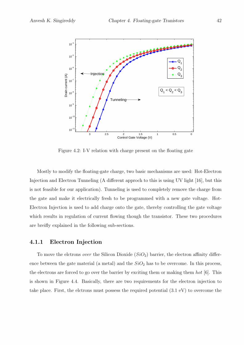
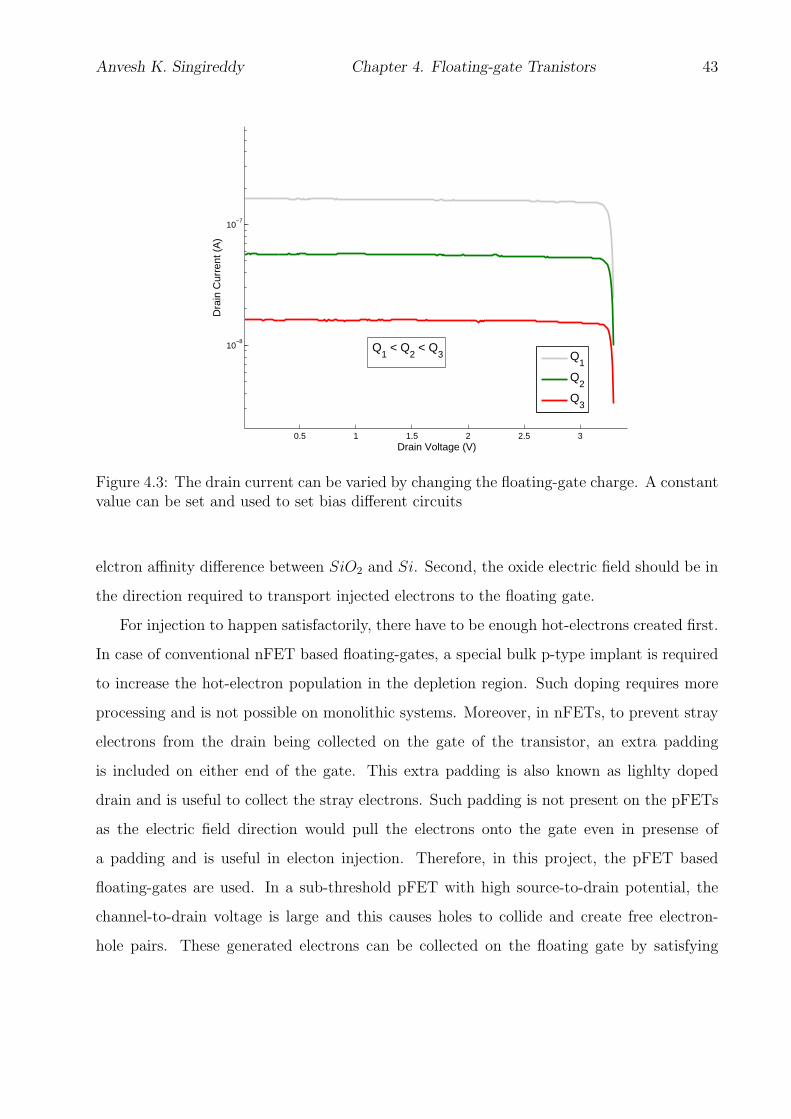
To program the circuits dynamically and to allow post-fabrcation reconfigurability we
need non-volatile memory elements which can store the charge to preserve the biasing con-
ditions and the inter-block connection configuration. For this, the floating-gate transistors
(Fig. 4.1) are used. A transistor in which the gate is electrically isolated can be defined as a
floating-gate transistor. The flow of electrons to and from the gate is restricted due to this
isolation. The secondary control-gate (Fig. 4.1) capcitively couples charge onto the isolated
(floating) gate and this results in the shift of the MOSFET’s tranfer function as illustrated
in Figures 4.2 and 4.3
Vs
Vd
Vtun
Floating Gate
Control Gate
Figure 4.1: Floating gate and Control gate
Anvesh K. Singireddy Chapter 4. Floating-gate Tranistors 42
00.511.522.53
10−11
10−10
10−9
10−8
10−7
10−6
10−5
10−4
Control Gate Voltage (V)
Dra
in c
urre
nt (
A)
Q1
Q2
Q3
Injection
Tunneling
Q1 < Q
2 < Q
3
Figure 4.2: I-V relation with charge present on the floating gate
Mostly to modify the floating-gate charge, two basic mechanisms are used: Hot-Electron
Injection and Electron Tunneling (A different approch to this is using UV light [16], but this
is not feasible for our application). Tunneling is used to completely remove the charge from
the gate and make it electrically fresh to be programmed with a new gate voltage. Hot-
Electron Injection is used to add charge onto the gate, thereby controlling the gate voltage
which results in regulation of current flowing though the transistor. These two procedures
are breifly explained in the following sub-sections.
4.1.1 Electron Injection
To move the elctrons over the Silicon Dioxide (SiO2) barrier, the electron affinity differ-
ence between the gate material (a metal) and the SiO2 has to be overcome. In this process,
the electrons are forced to go over the barrier by exciting them or making them hot [6]. This
is shown in Figure 4.4. Basically, there are two requirements for the electron injection to
take place. First, the elctrons must possess the required potential (3.1 eV) to overcome the
Anvesh K. Singireddy Chapter 4. Floating-gate Tranistors 43
0.5 1 1.5 2 2.5 3
10−8
10−7
Drain Voltage (V)
Dra
in C
urre
nt (
A)
Q1
Q2
Q3
Q1 < Q
2 < Q
3
Figure 4.3: The drain current can be varied by changing the floating-gate charge. A constantvalue can be set and used to set bias different circuits
elctron affinity difference between SiO2 and Si. Second, the oxide electric field should be in
the direction required to transport injected electrons to the floating gate.
For injection to happen satisfactorily, there have to be enough hot-electrons created first.
In case of conventional nFET based floating-gates, a special bulk p-type implant is required
to increase the hot-electron population in the depletion region. Such doping requires more
processing and is not possible on monolithic systems. Moreover, in nFETs, to prevent stray
electrons from the drain being collected on the gate of the transistor, an extra padding
is included on either end of the gate. This extra padding is also known as lighlty doped
drain and is useful to collect the stray electrons. Such padding is not present on the pFETs
as the electric field direction would pull the electrons onto the gate even in presense of
a padding and is useful in electon injection. Therefore, in this project, the pFET based
floating-gates are used. In a sub-threshold pFET with high source-to-drain potential, the
channel-to-drain voltage is large and this causes holes to collide and create free electron-
hole pairs. These generated electrons can be collected on the floating gate by satisfying
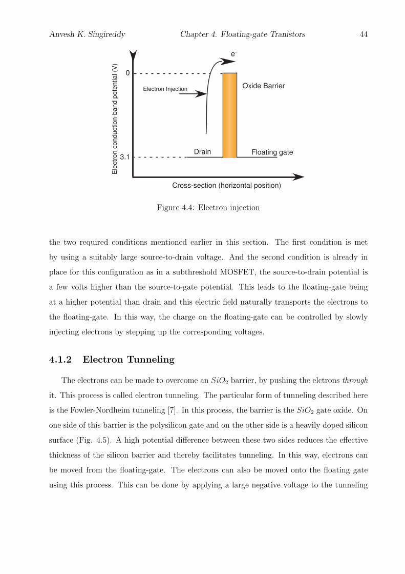
Anvesh K. Singireddy Chapter 4. Floating-gate Tranistors 44
Electron Injection
0
3.1
Ele
ctr
on
co
nd
uctio
n-b
an
d p
ote
ntia
l (V
)
Cross-section (horizontal position)
Floating gate
Oxide Barrier
Drain
e-
Figure 4.4: Electron injection
the two required conditions mentioned earlier in this section. The first condition is met
by using a suitably large source-to-drain voltage. And the second condition is already in
place for this configuration as in a subthreshold MOSFET, the source-to-drain potential is
a few volts higher than the source-to-gate potential. This leads to the floating-gate being
at a higher potential than drain and this electric field naturally transports the electrons to
the floating-gate. In this way, the charge on the floating-gate can be controlled by slowly
injecting electrons by stepping up the corresponding voltages.
4.1.2 Electron Tunneling
The electrons can be made to overcome an SiO2 barrier, by pushing the elctrons through
it. This process is called electron tunneling. The particular form of tunneling described here
is the Fowler-Nordheim tunneling [7]. In this process, the barrier is the SiO2 gate oxide. On
one side of this barrier is the polysilicon gate and on the other side is a heavily doped silicon
surface (Fig. 4.5). A high potential difference between these two sides reduces the effective
thickness of the silicon barrier and thereby facilitates tunneling. In this way, electrons can
be moved from the floating-gate. The electrons can also be moved onto the floating gate
using this process. This can be done by applying a large negative voltage to the tunneling
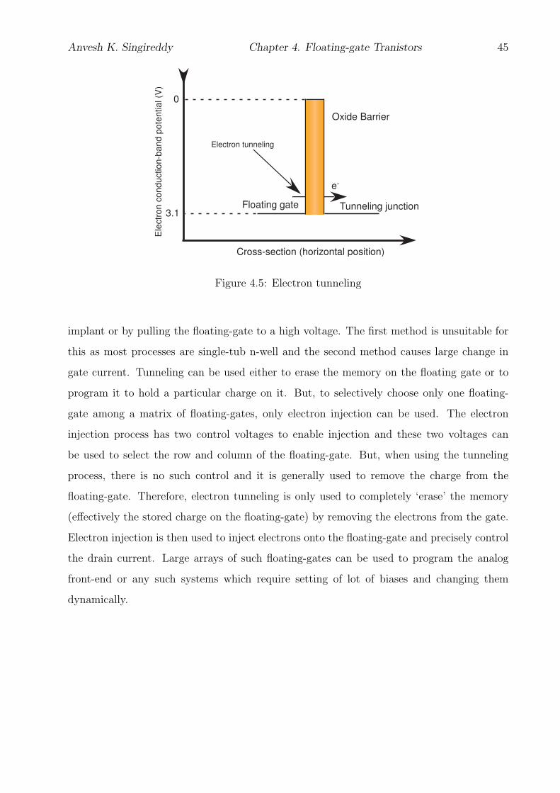
Anvesh K. Singireddy Chapter 4. Floating-gate Tranistors 45
Electron tunneling
0
3.1
Ele
ctr
on
co
nd
uctio
n-b
an
d p
ote
ntia
l (V
)
Cross-section (horizontal position)
Tunneling junction
Oxide Barrier
Floating gate
e-
Figure 4.5: Electron tunneling
implant or by pulling the floating-gate to a high voltage. The first method is unsuitable for
this as most processes are single-tub n-well and the second method causes large change in
gate current. Tunneling can be used either to erase the memory on the floating gate or to
program it to hold a particular charge on it. But, to selectively choose only one floating-
gate among a matrix of floating-gates, only electron injection can be used. The electron
injection process has two control voltages to enable injection and these two voltages can
be used to select the row and column of the floating-gate. But, when using the tunneling
process, there is no such control and it is generally used to remove the charge from the
floating-gate. Therefore, electron tunneling is only used to completely ‘erase’ the memory
(effectively the stored charge on the floating-gate) by removing the electrons from the gate.
Electron injection is then used to inject electrons onto the floating-gate and precisely control
the drain current. Large arrays of such floating-gates can be used to program the analog
front-end or any such systems which require setting of lot of biases and changing them
dynamically.
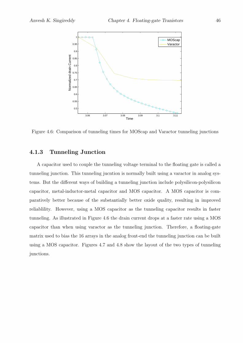
Anvesh K. Singireddy Chapter 4. Floating-gate Tranistors 46
3.06 3.07 3.08 3.09 3.1 3.11
0.5
0.55
0.6
0.65
0.7
0.75
0.8
0.85
0.9
0.95
1
Time
Nor
mal
ized
dra
in C
urre
nt
MOScapVaractor
Figure 4.6: Comparison of tunneling times for MOScap and Varactor tunneling junctions
4.1.3 Tunneling Junction
A capacitor used to couple the tunneling voltage terminal to the floating gate is called a
tunneling junction. This tunneling jucntion is normally built using a varactor in analog sys-
tems. But the different ways of building a tunneling junction include polysilicon-polysilicon
capacitor, metal-inductor-metal capacitor and MOS capacitor. A MOS capacitor is com-
paratively better because of the substantially better oxide quality, resulting in improved
reliablility. However, using a MOS capacitor as the tunneling capacitor results in faster
tunneling. As illustrated in Figure 4.6 the drain current drops at a faster rate using a MOS
capacitor than when using varactor as the tunneling junction. Therefore, a floating-gate
matrix used to bias the 16 arrays in the analog front-end the tunneling junction can be built
using a MOS capacitor. Figures 4.7 and 4.8 show the layout of the two types of tunneling
junctions.
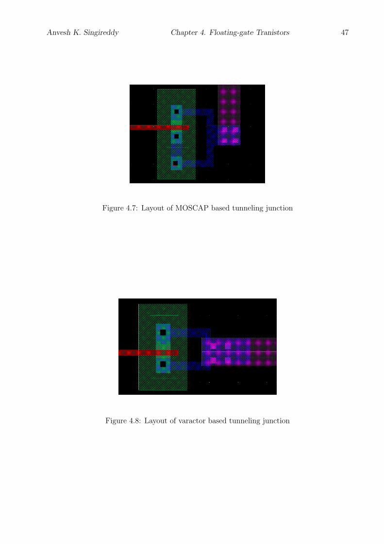
Anvesh K. Singireddy Chapter 4. Floating-gate Tranistors 47
Figure 4.7: Layout of MOSCAP based tunneling junction
Figure 4.8: Layout of varactor based tunneling junction
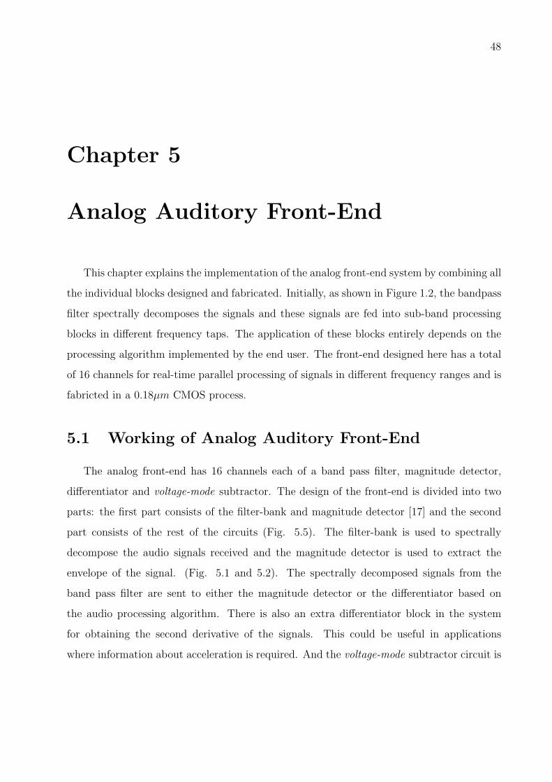
48
Chapter 5
Analog Auditory Front-End
This chapter explains the implementation of the analog front-end system by combining all
the individual blocks designed and fabricated. Initially, as shown in Figure 1.2, the bandpass
filter spectrally decomposes the signals and these signals are fed into sub-band processing
blocks in different frequency taps. The application of these blocks entirely depends on the
processing algorithm implemented by the end user. The front-end designed here has a total
of 16 channels for real-time parallel processing of signals in different frequency ranges and is
fabricted in a 0.18µm CMOS process.
5.1 Working of Analog Auditory Front-End
The analog front-end has 16 channels each of a band pass filter, magnitude detector,
differentiator and voltage-mode subtractor. The design of the front-end is divided into two
parts: the first part consists of the filter-bank and magnitude detector [17] and the second
part consists of the rest of the circuits (Fig. 5.5). The filter-bank is used to spectrally
decompose the audio signals received and the magnitude detector is used to extract the
envelope of the signal. (Fig. 5.1 and 5.2). The spectrally decomposed signals from the
band pass filter are sent to either the magnitude detector or the differentiator based on
the audio processing algorithm. There is also an extra differentiator block in the system
for obtaining the second derivative of the signals. This could be useful in applications
where information about acceleration is required. And the voltage-mode subtractor circuit is
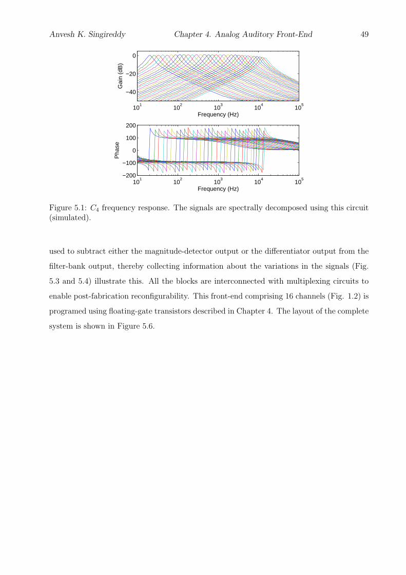
Anvesh K. Singireddy Chapter 4. Analog Auditory Front-End 49
101
102
103
104
105
−40
−20
0
Frequency (Hz)G
ain
(dB
)
101
102
103
104
105
−200
−100
0
100
200
Frequency (Hz)
Pha
se
Figure 5.1: C4 frequency response. The signals are spectrally decomposed using this circuit(simulated).
used to subtract either the magnitude-detector output or the differentiator output from the
filter-bank output, thereby collecting information about the variations in the signals (Fig.
5.3 and 5.4) illustrate this. All the blocks are interconnected with multiplexing circuits to
enable post-fabrication reconfigurability. This front-end comprising 16 channels (Fig. 1.2) is
programed using floating-gate transistors described in Chapter 4. The layout of the complete
system is shown in Figure 5.6.
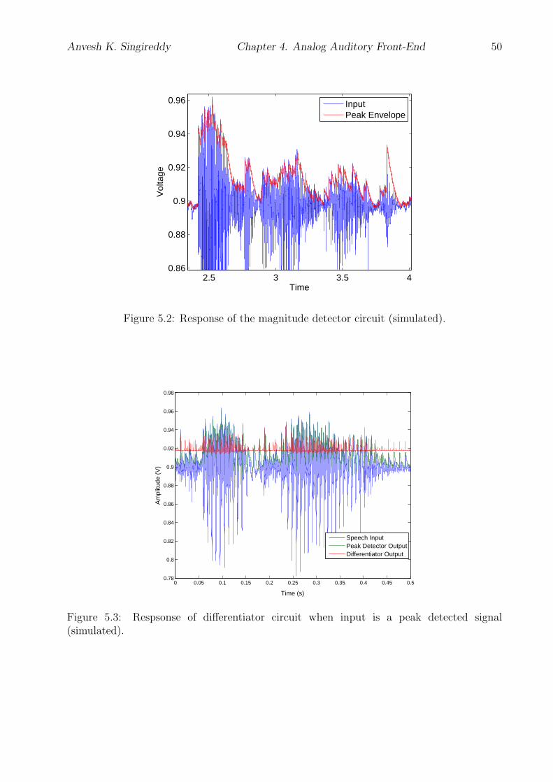
Anvesh K. Singireddy Chapter 4. Analog Auditory Front-End 50
2.5 3 3.5 40.86
0.88
0.9
0.92
0.94
0.96
Time
Vol
tage
InputPeak Envelope
Figure 5.2: Response of the magnitude detector circuit (simulated).
0 0.05 0.1 0.15 0.2 0.25 0.3 0.35 0.4 0.45 0.50.78
0.8
0.82
0.84
0.86
0.88
0.9
0.92
0.94
0.96
0.98
Time (s)
Am
plitu
de (
V)
Speech InputPeak Detector OutputDifferentiator Output
Figure 5.3: Respsonse of differentiator circuit when input is a peak detected signal(simulated).
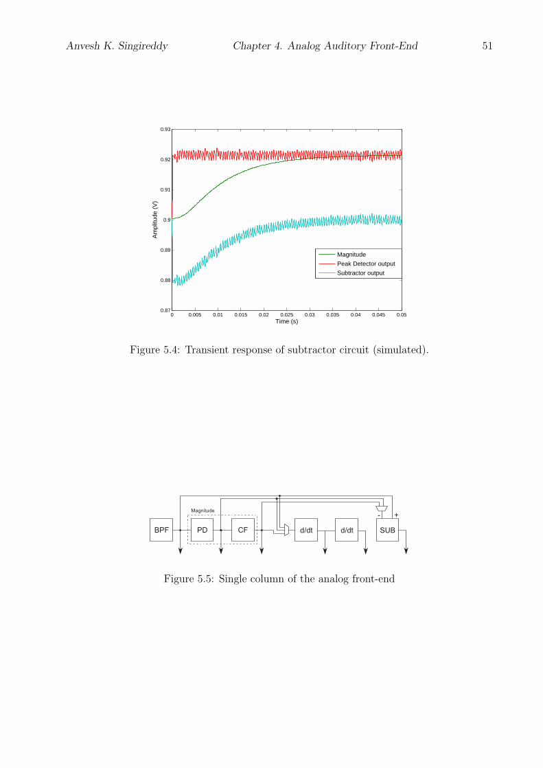
Anvesh K. Singireddy Chapter 4. Analog Auditory Front-End 51
0 0.005 0.01 0.015 0.02 0.025 0.03 0.035 0.04 0.045 0.050.87
0.88
0.89
0.9
0.91
0.92
0.93
Time (s)
Am
plitu
de (
V)
Magnitude
Peak Detector output
Subtractor output
Figure 5.4: Transient response of subtractor circuit (simulated).
BPF PD CF d/dt d/dt SUB
Magnitude+-
Figure 5.5: Single column of the analog front-end
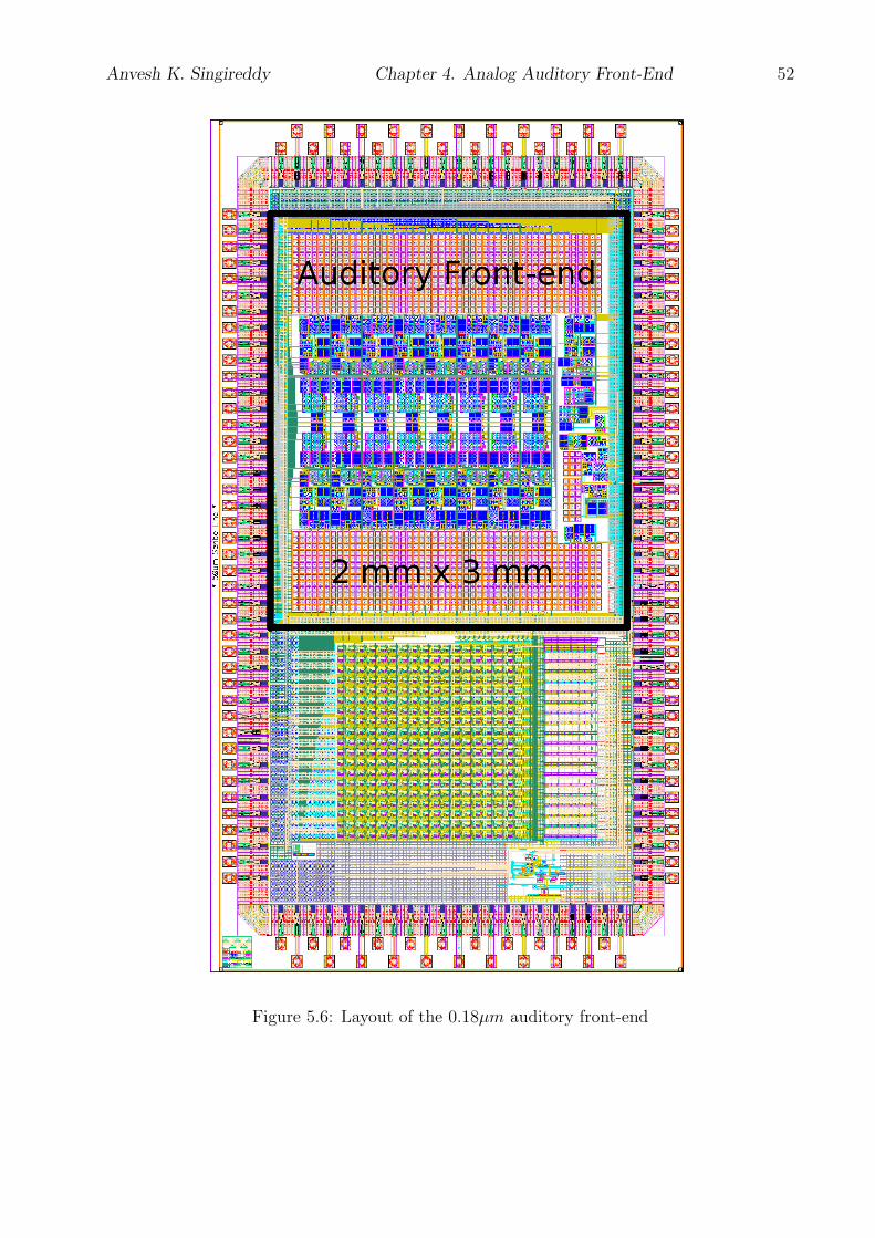
Anvesh K. Singireddy Chapter 4. Analog Auditory Front-End 52
Figure 5.6: Layout of the 0.18µm auditory front-end
53
Chapter 6
Applications and Conclusion
6.1 Low-Power Hardware-Based Event Detection
The analog auditory front-end system desinged here finds many applications in speech
recognition [18], sound localizing [19], noise supression [20] or hearing prosthesis [21]. One
of the many application areas is wireless sensor networks. This is a very suitable field of
application as power is at premium in such networks and also the contemporary sensor
nodes essentially have low computational abilities [22, 23, 24, 25]. The analog systems here
offer ultra-low-power alternatives when compared to digital counterparts for initial signal
processing [26, 27]. In addition to the low-power advantage, these systems also are able to
perform some signal analysis and free-up the power hungry digital systems for other higher-
level tasks.
In sensor networks, usually the maximum power consumption is by the radio or the
communication system. One good way to reduce this power is communicating only when
required and also transmitting only the relevant information rather than everything the
sensor detects. To acheive this, the radio is set to a sleep state until an event of interest
is detected by the mote sensors [28]. To communicate only the relevant informaiton, some
signal processing would be required on the mote itself and this is done by using the low-power
analog circuits. This chapter explains the details of this application and its advantages.
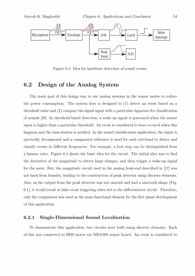
Anvesh K. Singireddy Chapter 6. Applications and Conclusion 54
Microphone Envelope d/dt Latch
Peak Hold
Mote Interrupt
A/D
Figure 6.1: Idea for hardware detection of sound events.
6.2 Design of the Analog System
The main goal of this design was to use analog systems in the sensor motes to reduce
the power consumption. The system here is designed to (1) detect an event based on a
threshold value and (2) compare the signal input with a particular signature for classification
of sounds [26]. In threshold-based detection, a wake-up signal is generated when the sensor
input is higher than a particular threshold. An event is considered to have occured when this
happens and the base-station is notified. In the sound classification application, the input is
spectrally decomposed and a comparator reference is used for each sub-band to detect and
classify events in different frequencies. For example, a foot step can be distinguished from
a human voice. Figure 6.1 shows the basic idea for the circuit. The initial idea was to find
the derivative of the magnitude to detect large changes, and then trigger a wake-up signal
for the mote. But, the magnitude circuit used in the analog front-end described in [17] was
not back from foundry, leading to the construction of peak detector using discrete elements.
Also, as the output from the peak detector was not smooth and had a sawtooth shape (Fig.
6.1), it would result in false event triggering when fed to the differentiator circuit. Therefore,
only the comparator was used as the main functional element for the first phase development
of this application.
6.2.1 Single-Dimensional Sound Localization
To demonstrate this application, two circuits were built using discrete elements. Each
of this was connected to IRIS motes via MDA300 sensor board. An event is considered to
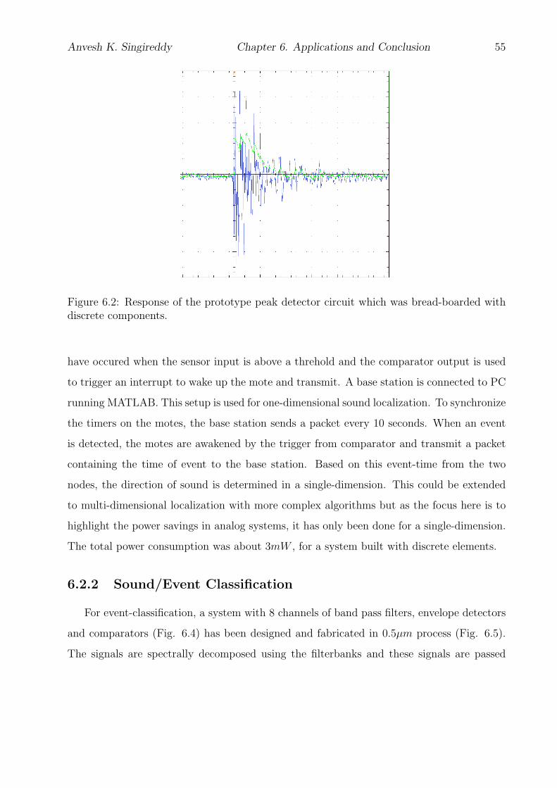
Anvesh K. Singireddy Chapter 6. Applications and Conclusion 55
Figure 6.2: Response of the prototype peak detector circuit which was bread-boarded withdiscrete components.
have occured when the sensor input is above a threhold and the comparator output is used
to trigger an interrupt to wake up the mote and transmit. A base station is connected to PC
running MATLAB. This setup is used for one-dimensional sound localization. To synchronize
the timers on the motes, the base station sends a packet every 10 seconds. When an event
is detected, the motes are awakened by the trigger from comparator and transmit a packet
containing the time of event to the base station. Based on this event-time from the two
nodes, the direction of sound is determined in a single-dimension. This could be extended
to multi-dimensional localization with more complex algorithms but as the focus here is to
highlight the power savings in analog systems, it has only been done for a single-dimension.
The total power consumption was about 3mW , for a system built with discrete elements.
6.2.2 Sound/Event Classification
For event-classification, a system with 8 channels of band pass filters, envelope detectors
and comparators (Fig. 6.4) has been designed and fabricated in 0.5µm process (Fig. 6.5).
The signals are spectrally decomposed using the filterbanks and these signals are passed
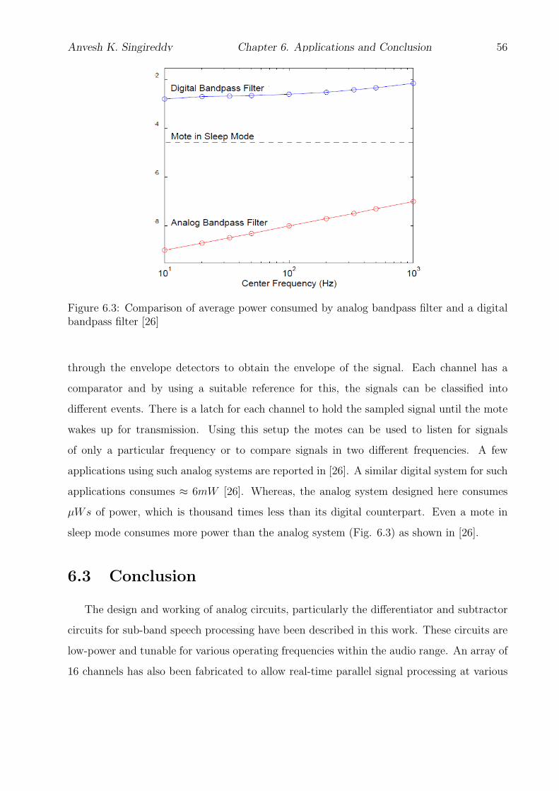
Anvesh K. Singireddy Chapter 6. Applications and Conclusion 56
Figure 6.3: Comparison of average power consumed by analog bandpass filter and a digitalbandpass filter [26]
through the envelope detectors to obtain the envelope of the signal. Each channel has a
comparator and by using a suitable reference for this, the signals can be classified into
different events. There is a latch for each channel to hold the sampled signal until the mote
wakes up for transmission. Using this setup the motes can be used to listen for signals
of only a particular frequency or to compare signals in two different frequencies. A few
applications using such analog systems are reported in [26]. A similar digital system for such
applications consumes ≈ 6mW [26]. Whereas, the analog system designed here consumes
µWs of power, which is thousand times less than its digital counterpart. Even a mote in
sleep mode consumes more power than the analog system (Fig. 6.3) as shown in [26].
6.3 Conclusion
The design and working of analog circuits, particularly the differentiator and subtractor
circuits for sub-band speech processing have been described in this work. These circuits are
low-power and tunable for various operating frequencies within the audio range. An array of
16 channels has also been fabricated to allow real-time parallel signal processing at various
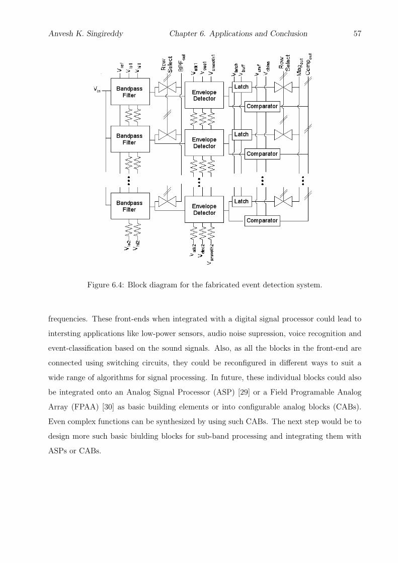
Anvesh K. Singireddy Chapter 6. Applications and Conclusion 57
Figure 6.4: Block diagram for the fabricated event detection system.
frequencies. These front-ends when integrated with a digital signal processor could lead to
intersting applications like low-power sensors, audio noise supression, voice recognition and
event-classification based on the sound signals. Also, as all the blocks in the front-end are
connected using switching circuits, they could be reconfigured in different ways to suit a
wide range of algorithms for signal processing. In future, these individual blocks could also
be integrated onto an Analog Signal Processor (ASP) [29] or a Field Programable Analog
Array (FPAA) [30] as basic building elements or into configurable analog blocks (CABs).
Even complex functions can be synthesized by using such CABs. The next step would be to
design more such basic biulding blocks for sub-band processing and integrating them with
ASPs or CABs.

Anvesh K. Singireddy Chapter 6. Applications and Conclusion 58
Figure 6.5: Die shot of the event detection chip. The area inside the pad frame measures1.5mm x 1.5mm
59
Appendix A
Cadence setup
Majority of the work in this thesis was done on the software suite from Cadence Inc. It
was used to run simulaitons, do the layout of circuits in various CMOS processes and also
build PCBs to test the fabricated ICs. This software suite was setup on systems with Ubuntu
(an open souorce version of Linux operating system), which is not officially supported by
Cadence. To do this, various customizations had to be done to make it work on this particular
version of Linux operating system. The final goal was to setup this software such that it
could be accessed from all the departmental laboratories. Initially a CentOS based system
was used as the license server but eventually, all the applications in the suite and the license
server were migrated to Ubuntu based operating system at West Virginia University, known
as LOUD (LCSEE Optimized Ubuntu Distribution). Presently this software suite can be
accessed from any of the departmental laboratories.
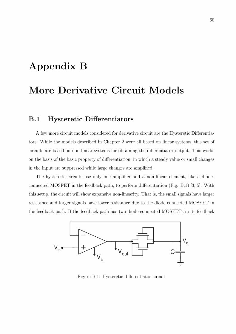
60
Appendix B
More Derivative Circuit Models
B.1 Hysteretic Differentiators
A few more circuit models considered for derivative circuit are the Hysteretic Differentia-
tors. While the models described in Chapter 2 were all based on linear systems, this set of
circuits are based on non-linear systems for obtaining the differentiator output. This works
on the basis of the basic property of differentiation, in which a steady value or small changes
in the input are suppressed while large changes are amplified.
The hysteretic circuits use only one amplifier and a non-linear element, like a diode-
connected MOSFET in the feedback path, to perform differentiation (Fig. B.1) [3, 5]. With
this setup, the circuit will show expansive non-linearity. That is, the small signals have larger
resistance and larger signals have lower resistance due to the diode connected MOSFET in
the feedback path. If the feedback path has two diode-connected MOSFETs in its feedback
Vin
Vc
Vb
CVout
Figure B.1: Hysteretic differentiator circuit
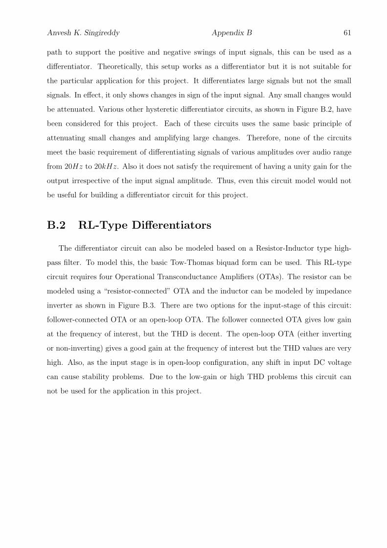
Anvesh K. Singireddy Appendix B 61
path to support the positive and negative swings of input signals, this can be used as a
differentiator. Theoretically, this setup works as a differentiator but it is not suitable for
the particular application for this project. It differentiates large signals but not the small
signals. In effect, it only shows changes in sign of the input signal. Any small changes would
be attenuated. Various other hysteretic differentiator circuits, as shown in Figure B.2, have
been considered for this project. Each of these circuits uses the same basic principle of
attenuating small changes and amplifying large changes. Therefore, none of the circuits
meet the basic requirement of differentiating signals of various amplitudes over audio range
from 20Hz to 20kHz. Also it does not satisfy the requirement of having a unity gain for the
output irrespective of the input signal amplitude. Thus, even this circuit model would not
be useful for building a differentiator circuit for this project.
B.2 RL-Type Differentiators
The differentiator circuit can also be modeled based on a Resistor-Inductor type high-
pass filter. To model this, the basic Tow-Thomas biquad form can be used. This RL-type
circuit requires four Operational Transconductance Amplifiers (OTAs). The resistor can be
modeled using a “resistor-connected” OTA and the inductor can be modeled by impedance
inverter as shown in Figure B.3. There are two options for the input-stage of this circuit:
follower-connected OTA or an open-loop OTA. The follower connected OTA gives low gain
at the frequency of interest, but the THD is decent. The open-loop OTA (either inverting
or non-inverting) gives a good gain at the frequency of interest but the THD values are very
high. Also, as the input stage is in open-loop configuration, any shift in input DC voltage
can cause stability problems. Due to the low-gain or high THD problems this circuit can
not be used for the application in this project.
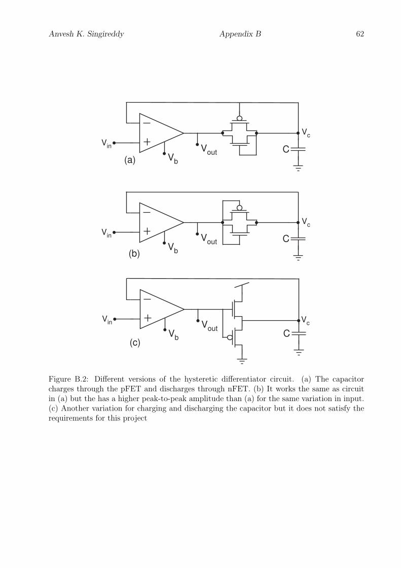
Anvesh K. Singireddy Appendix B 62
Vin
Vc
Vb
CVout
Vin
Vc
Vb
CVout
Vin V
c
Vb
C
Vout
(a)
(b)
(c)
Figure B.2: Different versions of the hysteretic differentiator circuit. (a) The capacitorcharges through the pFET and discharges through nFET. (b) It works the same as circuitin (a) but the has a higher peak-to-peak amplitude than (a) for the same variation in input.(c) Another variation for charging and discharging the capacitor but it does not satisfy therequirements for this project
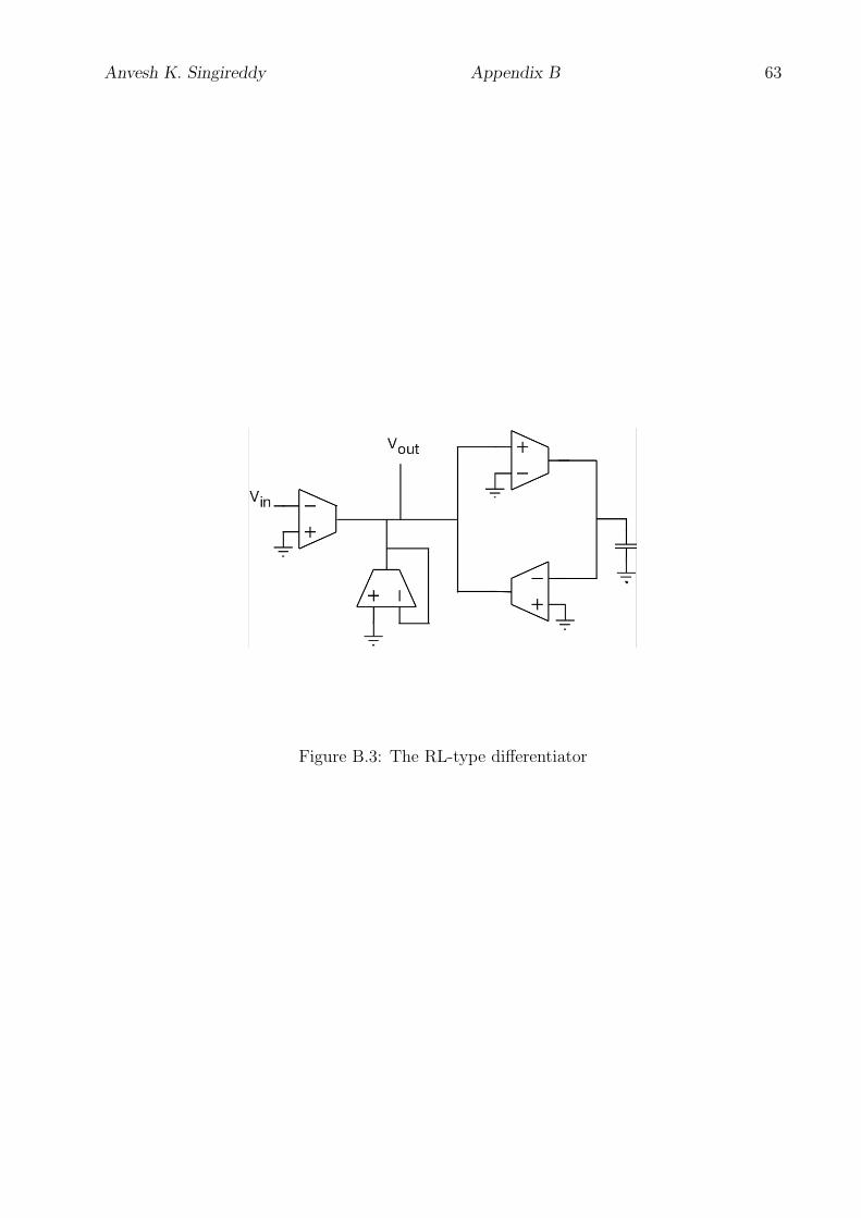
Anvesh K. Singireddy Appendix B 63
Figure B.3: The RL-type differentiator
64
References
[1] Behzad Razavi, Design of analog CMOS integrated circuits, McGraw Hill, 2001.
[2] Ivan A. Greenwood Jr., J. Vance Holdam Jr., and Duncan Machrae Jr., ElectronicInstruments, volume 21 of MIT Radiation Laboratory Series, McGraw-Hill, 1948.
[3] C. Mead, Analog VLSI and Neural Systems, Addison-Wesley, 1989.
[4] R. Fried and C.C. Enz, “Simple and accurate voltage adder/subtractor,” in ElectronicsLetters, May 1997, vol. 33, pp. 944–945.
[5] Jorg Kramer, Giacomo Indiveri, Tobias Delbruck, Shih-Chii Liu, and Rodney Douglas,Analog VLSI: Circuits and Principles, The MIT Press, 2002.
[6] Eiji Takeda, Cary Yang, and Akemi Miura-Hamada, Hot-Carrier effects in MOS devices,vol. optional of optional, Academic Press, Elsevier, optional, optional edition, November1995, optional.
[7] M. Lenzlinger and E. H. Snow, “Fowler-Nordheim Tunneling into Thermally GrownSiO2,” Journal of Applied Physics, vol. 40, pp. 278–283, Jan. 1969.
[8] C. Enz, F. Krummanacher, and E. Vittoz, “An analytical mos transistor model validin all regions of operation and dedicated to low-voltage and low-current applications,”Journal on Analog Integrated Circuits and Signal Processsing, , no. 1, pp. 83–114, July1995.
[9] David W. Graham and Paul Hasler, “Capacitively-coupled current conveyer second-order section for continuous-time bandpass filtering and cochlea modeling,” in Proceed-ings of the IEEE ISCAS, Atlanta, GA, 2002.
[10] A. Bouzerdoum, A. Yakovleff, D. Abbott, O. Kim, K. Eshraghian, A. Moini, and R.E.Bogner, “An analog implementation of early visual processing in insects,” in Proceedingsof International Symposium on VLSI Technology, Systems and Applications, 1993, pp.283–287.
[11] T. Delbruck and C. Mead, “Analog vlsi adaptive logarithmic wide-dynamic-range pho-toreceptor,” in Proceedings of the IEEE ISCAS, 1994, pp. 339–342.
[12] E.A. Vittoz, Analog VLSI computation of neural networks: Handbook of Neural Com-putation, Institute of Pyhsics Publishing and Oxford Univresity Press, USA.
REFERENCES 65
[13] A.S. Sedra and G.W. Roberts, “Current conveyor theory and practice,” Advances inAnalog Integrated Circuit Design, pp. 93–126, 1990.
[14] M.G. Johnson, “An input-free vt extractor circuit using a two-transistor differentialamplifier,” IEEE Journal of Solid-State Circuits, vol. 28, pp. 704–705, 1993.
[15] E.A. Vittoz, Micropower Techniques: Principles of Neural Science, Prentice-Hall, 1994.
[16] Douglas A. Kerns, John E. Tanner, Massimo A. Sivilotti, and Jin Luo, “Cmos uv-writable non-volatile analog storage,” in Proceedings of the 1991 University of Califor-nia/Santa Cruz conference on Advanced research in VLSI, Cambridge, MA, USA, 1991,pp. 245–261, MIT Press.
[17] Brandon Rumberg, “Speech processing front-end in low-power hardware,” M.S. thesis,West Virginia University, Morgantown, West Virginia, 2009.
[18] T. Massengill, D. Wilson, P. Hasler, and D. W. Graham, “Empirical comparison of ana-log and digital auditory preprocessing for automatic speech recognition,” in Proceedingsof the IEEE International Symposium on Circuits and Systems, Scottsdale, AZ, May2002, vol. 5, pp. 77–80.
[19] A. van Schaik and S. Shamma, “A neuromorphic sound localizer for a smart MEMSsystem,” in Proceedings of the International Symposium on Circuits and Systems, May2003, vol. 4, pp. IV–864–IV–867.
[20] R. Ellis, H. Yoo, D. W. Graham, P. Hasler, and D. V. Anderson, “A continuous-timespeech enhancement front-end for microphone inputs,” in Proceedings of the IEEEInternational Symposium on Circuits and Systems, Scottsdale, AZ, May 2002, vol. 2,pp. II–728–II–731.
[21] Rahul Sarpeshkar, Christopher Salthouse, Ji jon Sit, Michael W. Baker, Serhii M. Zhak,Timothy K. -t. Lu, Lorenzo Turicchia, and Stephanie Balster, “An ultra-low-powerprogrammable analog bionic ear processor,” in IEEE Transactions on Biomedical En-gineering, 2005, pp. 711–727.
[22] Anish Arora, Rajiv Ramnath, Emre Ertin, Prasun Sinha, Sandip Bapat, Vinayak Naik,and Vinod Kulathumani, “Exscal: Elements of an extreme scale wireless sensor net-work,” in RTCSA ’05: Proceedings of the 11th IEEE International Conference on Em-bedded and Real-Time Computing Systems and Applications, Washington, DC, USA,2005, pp. 102–108, IEEE Computer Society.
[23] Marco F. Duarte and Yu Hen Hu, “Vehicle classification in distributed sensor networks,”Journal of Parallel and Distributed Computing, vol. 64, no. optional, pp. 826–838, July2004, optional.
[24] V. Raghunathan, C. Schurgers, Sung Park, and M.B. Srivastava, “Energy-aware wirelessmicrosensor networks,” Signal Processing Magazine, IEEE, vol. 19, no. 2, pp. 40–50,mar 2002.
REFERENCES 66
[25] Ning Xu, Sumit Rangwala, Krishna Kant Chintalapudi, Deepak Ganesan, Alan Broad,Ramesh Govindan, and Deborah Estrin, “A wireless sensor network for structural mon-itoring,” in SenSys ’04: Proceedings of the 2nd international conference on Embeddednetworked sensor systems, New York, NY, USA, 2004, pp. 13–24, ACM.
[26] Brandon Rumberg, David Graham, and Vinod Kulathumani, “Hibernets: Energy-efficient sensor networks using analog signal processing,” in Proceedings of InternationalConference on Information Processing in Sensor Networks, Stockholm, Sweden, 2010(accepted).
[27] Rahul Sarpeshkar, “Analog versus digital: extrapolating from electronics to neurobiol-ogy,” Neural Comput., vol. 10, no. 7, pp. 1601–1638, 1998.
[28] S. Jevtic, M. Kotowsky, R.P. Dick, P.A. Dindap, and C. Dowding, “Lucid dreaming:reliable analog event detection for energy-constrained applications,” Piscataway, NJ,USA, 2007/04/, pp. 350–359.
[29] P. Hasler, P. Smith, D. Graham, R. Ellis, and D. Anderson, “Analog floating-gate, on-chip auditory sensing system interfaces,” IEEE Sensors Journal, vol. 5, pp. 1027–1034,October 2005.
[30] T.S. Hall, C.M. Twigg, J.D. Gray, P. Hasler, and D.V. Anderson, “Large-scale field-programmable analog arrays for analog signal processing,” Circuits and Systems I:Regular Papers, IEEE Transactions on, vol. 52, no. 11, pp. 2298–2307, nov. 2005.
Low-Power Analog Circuits for Sub-Band
Speech Processing
by
Anvesh Kumar Singireddy
Thesis submitted to theCollege of Engineering and Mineral Resources
at West Virginia Universityin partial fulfillment of the requirements for the degree of
Master of Sciencein
Electrical Engineering
Lane Department of Computer Science and Electrical Engineering
APPROVAL OF THE EXAMINING COMMITTEE
Dimitris Korakakis, Ph.D.
Jeremy Dawson, Ph.D.
David W. Graham, Ph.D., Chair
Date