Low Noise, Low Power Variable Gain Amplifier for...
9
Low Noise, Variable Gain Ampli TRA Fac Com Dep Adrian-Virgi Corporate Technology Siemens SRL, Romania Joint International Confere Optimization of Ele Aegean Conference on Electrical M May 25-27, 2017, Brașov, Low Power ifier for Ultrasounds ANSILVANIA University of BRAŞOV culty of Electrical Engineering and mputer Science partment of Electronics and Computers il CRĂCIUN ence OPTIM – ACEMP 2017 ectrical & Electronic Equipment Machines and Power Electronics Moieciu-Fundata ”Cheile Grădiștei”
Transcript of Low Noise, Low Power Variable Gain Amplifier for...

Low Noise, Low PowerVariable Gain Amplifier for Ultrasounds
TRANSILVANIAFaculty of Electrical Engineering andComputer ScienceDepartment of Electronics and Computers
Adrian-Virgil
Corporate TechnologySiemens SRL, Romania
Joint International Conference OPTIMOptimization of Electrical & Electronic Equipment
Aegean Conference on Electrical Machines and Power ElectronicsMay 25-27, 2017, Brașov, Moieciu
Low Noise, Low PowerVariable Gain Amplifier for Ultrasounds
TRANSILVANIA University of BRAŞOVFaculty of Electrical Engineering andComputer ScienceDepartment of Electronics and Computers
Virgil CRĂCIUN
Joint International Conference OPTIM – ACEMP 2017Optimization of Electrical & Electronic Equipment
Aegean Conference on Electrical Machines and Power Electronics27, 2017, Brașov, Moieciu-Fundata ”Cheile Grădiștei”

General presentation• This paper presents the simulation of a variable gain amplifier from three perspectives:
- functional, using LTspice circuit simulator;- signal-to-noise-ratio, computed with Excel and- power consumption, estimated with ACEplorer power simulator.
• The architectural decisions are taken based on these simulations to meet the requirements:- a dynamic range greater than 60 dB;- a frequency domain of 100 kHz to 3 MHz;- power consumption lower than 20 mW and- the signal to noise ratio greater than 12 dB (for an input sensitivity better than 50 microvolts).
• The analog part of the portableultrasonic measurement systemsconsists on a transmission (TX) chainand a receiver (RX) chain.
• The delay between TX and RX signalis measured; to have good results theoutput of TX chain (with a peak voltageof 13 V) is send also to the input of RXchain. The voltage range at thepreamplifier input will be from tens ofmicrovolts to volts (5 decade);
General presentationThis paper presents the simulation of a variable gain amplifier from three perspectives:
ratio, computed with Excel andpower consumption, estimated with ACEplorer power simulator.
The architectural decisions are taken based on these simulations to meet the requirements:
the signal to noise ratio greater than 12 dB (for an input sensitivity better than 50 microvolts).
Symplified Block diagram of the system

The RX Variable Gain Amplifier• The preliminary architecture presented in figure consists on: the buffer, the preamplifier and theVGA; three stages VGA has been considered with a gain of 0 to 24 dB each; that gives a gainvariation of 72 dB (3x24); an additional requirement is to vary the gain in steps of 3 dB to usemore than 70% of the ADC range. A possible allocation of gains for the 3 stages is:
• 24 / 15 / 9 / 0 dB for one stage;• 24 / 18 / 6 / 0 dB for another stage;• 24 / 21 / 3 / 0 dB for the other stage.
• The preamplifier gain should begreater than 11 dB (for the minimumsensitivity of 50 microvolts) and theattenuation (for the maximum inputof 10 V) should be less than -23 dB.The preliminary preamplifier gains(and attenuations) are:
• 12 / 6 / -9 / -24 dB; the twointermediate values can bemodified according to otherpossible needs.
The RX Variable Gain AmplifierThe preliminary architecture presented in figure consists on: the buffer, the preamplifier and the
VGA; three stages VGA has been considered with a gain of 0 to 24 dB each; that gives a gainvariation of 72 dB (3x24); an additional requirement is to vary the gain in steps of 3 dB to usemore than 70% of the ADC range. A possible allocation of gains for the 3 stages is:
Block diagram of the RX amplifier
Stability of CFAThe circuit used to analyze the stability is
presented in the next figure. The signalinjection point is not relevant from the stabilitypoint of view; the input was grounded.
The stability has been evaluated at the point ofintersection of the open-loop gain (Z) with theideal closed-loop gain (1/b) – 0dB point of theloop gain.
The feedback impedance used by invertingconfiguration consists on a 4.7kW resistor inparallel with a 4.7 pF capacitor, used to filterthe alias frequency – red line in the figure.
FZGZ
oV
1I 2I
+
-
ZB
G=1
G=1I
Z I.
I-
I-
Stability of CFA
With the 4.7 kW feedback resistor and withthe minimum gain case, the filtering frequencywill be of 1.2 MHz; at the intersections of anequivalent 1/b value of 99dBW (79dBW + 20dBW)with the open-loop characteristic – yellow line.
Based on these analyses a separate filter(instead of CF) would be a good alternative.
Graphical stability analysis realized on the gain-frequency CFA characteristic (ADG8005)
fP=7MHzfZ=127MHzto 267MHz
RF=500W
79
544
RF=4.7kWCF=4.7pF
86 RF=10kW
99
fP=1.2MHz
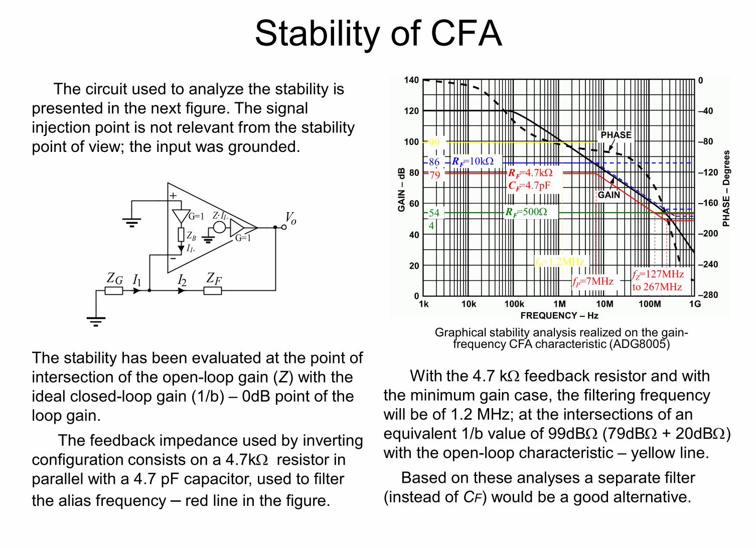
Limiting of Bandwidth
Simulation circuit for the 2nd order active filter with MUX
Filters are used to reduce the bandwidth (BW); that will reduce the input noise and increase thesignal-to-noise ratio. In this analysis a switchable filters is proposed.
A KRC (Salen-Key) active filter is considered since it does not require reactive elements in the(negative) feedback path, which would compromise stability of CFA.
A solution for the filter was calculated to cover the frequency domain with 4 set of values andwith a gain of 6 dB at the center frequency of the filter. The low and high frequency wereestimated with a quality factor of 1. Simulation and theoretical results are compared in next table.
Limiting of Bandwidth); that will reduce the input noise and increase the
noise ratio. In this analysis a switchable filters is proposed.Key) active filter is considered since it does not require reactive elements in the
(negative) feedback path, which would compromise stability of CFA.
A solution for the filter was calculated to cover the frequency domain with 4 set of values andwith a gain of 6 dB at the center frequency of the filter. The low and high frequency wereestimated with a quality factor of 1. Simulation and theoretical results are compared in next table.
Theoretical and simulation results for 3 set of values
The analog MUX effect is the reduction ofthe gain (H0) at the central frequency whenfilter frequency decrease. This effect wascompensated by adjusting the componentvalues and verify by simulation.
Th Sim Th Sim Th Simf0 (MHz) 1 1 2 1.99 0.5 0.5
R3 (W) 1k 1k 250 249 4k 4020K0 2.67 - 6.67 - 1.67 -
RG (W) 600 590 176 124 1.5k 1500Q 1.06 1.06 0.85 0.9 0.85 0.82
H0 (dB) 6.0 6.1 6.0 6.06 6.0 5.8BW (MHz) 0.94 0.94 2.36 2.2 0.59 0.61
Signal to Noise Ratio Analysis
Signal-to-Noise-Ratio for different positions of BPF
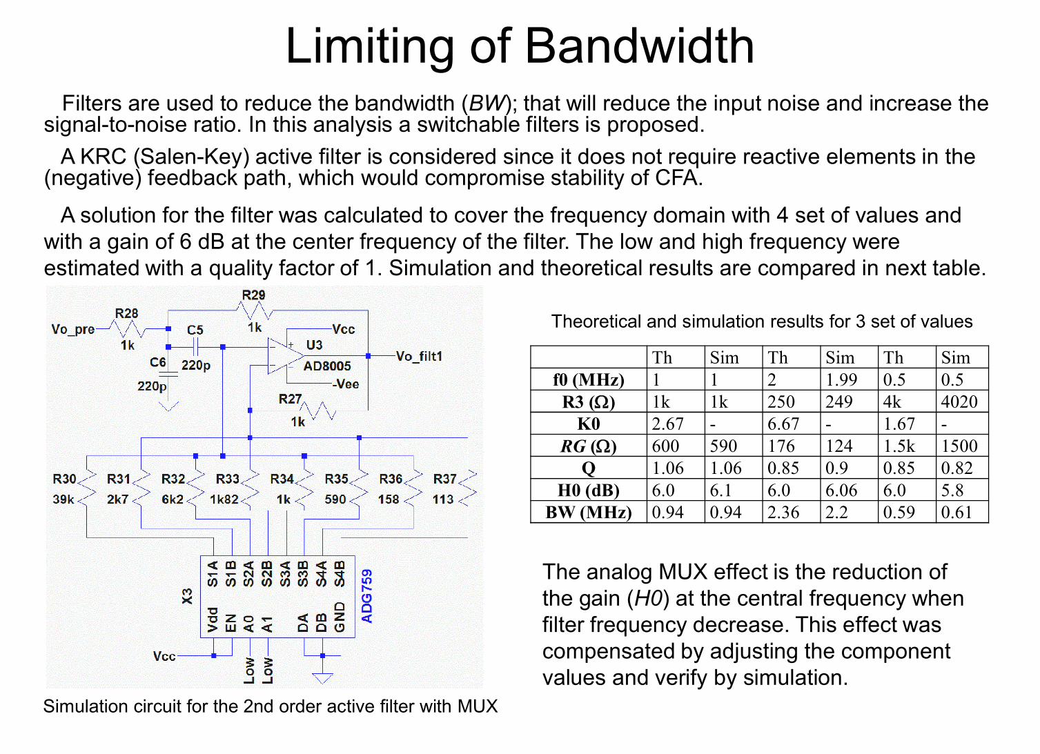
The RX buffer and preamplifier determinethe input noise and the SNR of the wholecircuit. To get a good SNR, the buffer circuitis realized with low noise transistors and thepreamplifier circuit is realized with the lownoise AD8014 CFA. The band pass filter(BPF) position influences the noise.
The results of the Excel noise model forthe lower bandwidth (BW) of the BPF arepresented in next figure.
Signal to Noise Ratio AnalysisThe worst cases are with the BPF at the
input of the circuit and without BPF. The bestcase, for all VGA gains, is with the BPF afterthe VGA.
The whole RX chain is modeled in Excel; itcontains the actual circuits with the buffer, thepreamplifier, the VGA and the BPF.
The simulation results presented in figureare with the BPF set at the 1st position (with aBW of 0.65 MHz). At the center frequency ofthe BPF, the input sensitivity is 45 micro-volts,with a corresponding SNR of 18.5 dB.
Signal-to-Noise-Ratio for the RX chain

Signal to Noise Ratio Computing
Excel table for computing the Signal
Signal to Noise Ratio Computing
Excel table for computing the Signal-to-Noise-Ratio of the RX chain

The power scenario description is based onthe operating use-case that specifies theexecution order and timing information.
The sequence of operation is periodicallyexecuted with a transmission phase of 50 msand a receiving phase of 0.5 ms.
Scenario description in Aceplorer (a Docea Intel tool)
Block diagram of the RX chain and of the VGA macro-component
Power SimulationPower Simulation
Power distribution of RX chain in time
The scenario was coded with TX activitiesand RX activities in parallel as indicated in thefigure. The scenario elements are the delay(indicate time), the stamp (indicates powerstates and programmable values), the step(indicates the time and the power operations)and job (a container for other elements).
The average values of VGA part / RX chainfor the presented scenario are 11.8 / 36.7 mW(with a minimum of 10.4 / 24.8 mW and amaximum of 22.9 / 609 mW).

ConclusionsThis paper present the architecture and implementation details for an ultrasound variable gain
amplifier with low power consumption and low noise for:• a frequency domain of 100 kHz to 4 MHz,• a gain variation of 72 dB.• A signal-to-noise ratio better than 18.5 dB for an input sensitivity of 45 mV;• Worst case average power consumption is 12
The proposed circuit is realized with low power current feedback amplifiers and consists on:• a preamplifier with AD8014 with a gain of: -• a switchable band-pass filter with AD8005 with 6 dB gain and center frequencies of:0.2, 0.4, 1 and 2.5 MHz,• 3 VGA stages with AD8005, with a gain of 0 to 24 dB, digitally controlled in 3 dB steps.
The circuit was designed starting from theoretical analysis and was verified by differentsimulations:
• LT-spice functional simulation,• Aceplorer, (a Docea Intel tool) used for power simulation,• Excel estimation and LT-spice noise simulation.
It was analyzed the current feedback amplifier stability. The noise was reduced by limiting thebandwidth with a dedicated switchable filter. The simulation results validate the proposed circuit.
The typical quiescent power consumption is 5total typical power of about 12 mW; that is lower than the dedicated VGA integrated circuits.
ConclusionsThis paper present the architecture and implementation details for an ultrasound variable gain
amplifier with low power consumption and low noise for:
noise ratio better than 18.5 dB for an input sensitivity of 45 mV;Worst case average power consumption is 12 mW
The proposed circuit is realized with low power current feedback amplifiers and consists on:-19, 0, 15 and 21 dB,
pass filter with AD8005 with 6 dB gain and center frequencies of:
3 VGA stages with AD8005, with a gain of 0 to 24 dB, digitally controlled in 3 dB steps.The circuit was designed starting from theoretical analysis and was verified by different
Intel tool) used for power simulation,spice noise simulation.
It was analyzed the current feedback amplifier stability. The noise was reduced by limiting thebandwidth with a dedicated switchable filter. The simulation results validate the proposed circuit.
The typical quiescent power consumption is 5 mW for AD8014 and 1.75 mW for AD8005, with a; that is lower than the dedicated VGA integrated circuits.