
Low Input Voltage Synchronous Boost Converter with 1.3 A ... · VIN L EN UVLO PS GND PGND FB VAUX...
35
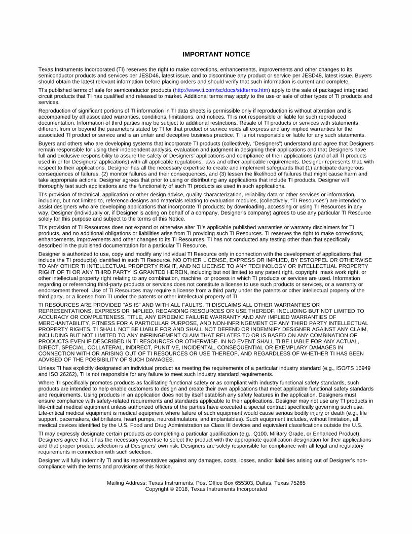
L VIN EN UVLO PS GND PGND FB VAUX VOUT TPS61200 VIN 0.3 V to 5.5 V VOUT 1.8 V to 5.5 V 10 F m 10 F m 2.2 H m 0.1 F m C 1 C 2 C 3 L 1 R 1 R 2 Product Folder Sample & Buy Technical Documents Tools & Software Support & Community TPS61200, TPS61201, TPS61202 SLVS577E – MARCH 2007 – REVISED DECEMBER 2014 TPS6120x Low Input Voltage Synchronous Boost Converter With 1.3-A Switches 1 Features 3 Description The TPS6120x devices provide a power supply 1• More than 90% Efficiency at solution for products powered by either a single-cell, – 300 mA Output Current at 3.3 V two-cell, or three-cell alkaline, NiCd or NiMH, or one- (VIN ≥ 2.4 V) cell Li-Ion or Li-polymer battery. It is also used in fuel – 600 mA Output Current at 5 V (VIN ≥ 3 V) cell or solar cell powered devices where the capability of handling low input voltages is essential. Possible • Automatic Transition between Boost Mode and output currents depend on the input to output voltage Down Conversion Mode ratio. The devices provide output currents of up to • Device Quiescent Current Less than 55 μA 600 mA at a 5-V output, while using a single-cell Li- • Startup into Full Load at 0.5 V Input Voltage Ion or Li-Polymer battery and discharges it down to 2.6 V. The boost converter is based on a fixed • Operating Input Voltage Range from frequency, pulse-width-modulation (PWM) controller 0.3 V to 5.5 V using synchronous rectification to obtain maximum • Programmable Undervoltage Lockout Threshold efficiency. At low load currents, the converter enters • Output Short Circuit Protection Under all the Power Save mode to maintain a high efficiency Operating Conditions over a wide load current range. The Power Save mode can be disabled, forcing the converter to • Fixed and Adjustable Output Voltage Options from operate at a fixed switching frequency. The average 1.8 V to 5.5 V input current is limited to a maximum value of 1500 • Power Save Mode for Improved Efficiency at Low mA. The output voltage is programmed by an Output Power external resistor divider, or is fixed internally on the chip. The converter can be disabled to minimize • Forced Fixed Frequency Operation Possible battery drain. During shutdown, the load is completely • Load Disconnect During Shutdown disconnected from the battery. The device is • Overtemperature Protection packaged in a 10-pin VSON package measuring 3 • Small 3 mm x 3 mm VSON-10 Package mm x 3 mm. Device Information (1) 2 Applications PART NUMBER PACKAGE BODY SIZE (NOM) • All Single-Cell, Two-Cell and Three-Cell Alkaline, TPS6120x VSON (10) 3.00 mm × 3.00 mm NiCd or NiMH or Single-Cell Li Battery Powered Products (1) For all available packages, see the orderable addendum at the end of the datasheet. • Fuel Cell And Solar Cell Powered Products • Portable Audio Players • PDAs • Cellular Phones • Personal Medical Products • White LED Driver 4 Typical Application 1 An IMPORTANT NOTICE at the end of this data sheet addresses availability, warranty, changes, use in safety-critical applications, intellectual property matters and other important disclaimers. PRODUCTION DATA.
Transcript of Low Input Voltage Synchronous Boost Converter with 1.3 A ... · VIN L EN UVLO PS GND PGND FB VAUX...
LVIN
EN
UVLO
PS
GND PGND
FB
VAUX
VOUT
TPS61200
VIN
0.3 V to 5.5 VVOUT
1.8 V to 5.5 V
10 Fm
10 Fm
2.2 Hm
0.1 Fm
C1
C2
C3
L1
R1
R2
Product
Folder
Sample &Buy
Technical
Documents
Tools &
Software
Support &Community
TPS61200, TPS61201, TPS61202SLVS577E –MARCH 2007–REVISED DECEMBER 2014
TPS6120x Low Input Voltage Synchronous Boost ConverterWith 1.3-A Switches
1 Features 3 DescriptionThe TPS6120x devices provide a power supply
1• More than 90% Efficiency atsolution for products powered by either a single-cell,– 300 mA Output Current at 3.3 V two-cell, or three-cell alkaline, NiCd or NiMH, or one-
(VIN ≥ 2.4 V) cell Li-Ion or Li-polymer battery. It is also used in fuel– 600 mA Output Current at 5 V (VIN ≥ 3 V) cell or solar cell powered devices where the capability
of handling low input voltages is essential. Possible• Automatic Transition between Boost Mode andoutput currents depend on the input to output voltageDown Conversion Moderatio. The devices provide output currents of up to
• Device Quiescent Current Less than 55 μA 600 mA at a 5-V output, while using a single-cell Li-• Startup into Full Load at 0.5 V Input Voltage Ion or Li-Polymer battery and discharges it down to
2.6 V. The boost converter is based on a fixed• Operating Input Voltage Range fromfrequency, pulse-width-modulation (PWM) controller0.3 V to 5.5 Vusing synchronous rectification to obtain maximum
• Programmable Undervoltage Lockout Threshold efficiency. At low load currents, the converter enters• Output Short Circuit Protection Under all the Power Save mode to maintain a high efficiency
Operating Conditions over a wide load current range. The Power Savemode can be disabled, forcing the converter to• Fixed and Adjustable Output Voltage Options fromoperate at a fixed switching frequency. The average1.8 V to 5.5 Vinput current is limited to a maximum value of 1500
• Power Save Mode for Improved Efficiency at Low mA. The output voltage is programmed by anOutput Power external resistor divider, or is fixed internally on the
chip. The converter can be disabled to minimize• Forced Fixed Frequency Operation Possiblebattery drain. During shutdown, the load is completely• Load Disconnect During Shutdowndisconnected from the battery. The device is
• Overtemperature Protection packaged in a 10-pin VSON package measuring 3• Small 3 mm x 3 mm VSON-10 Package mm x 3 mm.
Device Information(1)2 ApplicationsPART NUMBER PACKAGE BODY SIZE (NOM)• All Single-Cell, Two-Cell and Three-Cell Alkaline,
TPS6120x VSON (10) 3.00 mm × 3.00 mmNiCd or NiMH or Single-Cell Li Battery PoweredProducts (1) For all available packages, see the orderable addendum at
the end of the datasheet.• Fuel Cell And Solar Cell Powered Products• Portable Audio Players• PDAs• Cellular Phones• Personal Medical Products• White LED Driver
4 Typical Application
1
An IMPORTANT NOTICE at the end of this data sheet addresses availability, warranty, changes, use in safety-critical applications,intellectual property matters and other important disclaimers. PRODUCTION DATA.

TPS61200, TPS61201, TPS61202SLVS577E –MARCH 2007–REVISED DECEMBER 2014 www.ti.com
Table of Contents10.3 Feature Description............................................... 121 Features .................................................................. 110.4 Device Functional Modes...................................... 132 Applications ........................................................... 1
11 Application and Implementation........................ 143 Description ............................................................. 111.1 Application Information.......................................... 144 Typical Application ................................................ 111.2 Typical Application ............................................... 145 Revision History..................................................... 211.3 System Examples ................................................. 196 Device Options....................................................... 4
12 Power Supply Recommendations ..................... 207 Pin Configuration and Functions ......................... 413 Layout................................................................... 218 Specifications......................................................... 5
13.1 Layout Guidelines ................................................. 218.1 Absolute Maximum Ratings ...................................... 513.2 Layout Example .................................................... 218.2 ESD Ratings.............................................................. 513.3 Thermal Considerations ........................................ 218.3 Recommended Operating Conditions....................... 5
14 Device and Documentation Support ................. 228.4 Thermal Information .................................................. 514.1 Related Links ........................................................ 228.5 Electrical Characteristics........................................... 614.2 Trademarks ........................................................... 228.6 Typical Characteristics .............................................. 714.3 Electrostatic Discharge Caution............................ 229 Parameter Measurement Information ................ 1014.4 Glossary ................................................................ 2210 Detailed Description ........................................... 11 15 Mechanical, Packaging, and Orderable10.1 Overview ............................................................... 11 Information ........................................................... 22
10.2 Functional Block Diagram ..................................... 11
5 Revision HistoryNOTE: Page numbers for previous revisions may differ from page numbers in the current version.
Changes from Revision D (March 2013) to Revision E Page
• Added ESD Ratings table, Feature Description section, Device Functional Modes, Application and Implementationsection, Power Supply Recommendations section, Layout section, Device and Documentation Support section, andMechanical, Packaging, and Orderable Information section .................................................................................................. 1
Changes from Revision C (September 2012) to Revision D Page
• Changed the PS pin description From: Enable/disable Power Save mode (High = enabled, Low = disabled) To:Enable/disable Power Save mode (High = disabled, Low = enabled) ................................................................................... 4
Changes from Revision B (FEBRUARY 2008) to Revision C Page
• Changed Feature From: Small 3 mm x 3 mm QFN-10 Package To: Small 3 mm x 3 mm SON-10 Package ...................... 1• Changed Application From: White LED's To: White LED Driver ............................................................................................ 1• Changed the Available Device Options Package type From: 10-PIN QFN To: 10-Pin SON................................................. 4• Changed VSS to VIN in the Recommended Operating Conditions table ................................................................................. 5• Changed From: DISSIPATION RATINGS TABLE To: Thermal Information table ................................................................ 5• Changed the Parameters and Test Conditions in the Electrical Characteristics table .......................................................... 6• Updated Figure 1 through Figure 11 ...................................................................................................................................... 7• Added C3 to the List of Components ................................................................................................................................... 14• Added text to the Input Capacitor section "An R-C filter may be placed..." ......................................................................... 16• Added Figure 26, Figure 27, and Figure 28 ......................................................................................................................... 19• Added Figure 29 ................................................................................................................................................................... 21
2 Submit Documentation Feedback Copyright © 2007–2014, Texas Instruments Incorporated
Product Folder Links: TPS61200 TPS61201 TPS61202
TPS61200, TPS61201, TPS61202www.ti.com SLVS577E –MARCH 2007–REVISED DECEMBER 2014
Changes from Revision A (JUNE 2007) to Revision B Page
• Added DSC package and tape and reel note to the Available Device Options. .................................................................... 4
Changes from Original (MARCH 2007) to Revision A Page
• Changed Features bullet From: 600 mA Output Current at 3.3 V (VIN ≥ 1.2 V) To: 300 mA Output Current at 3.3 V(VIN ≥ 2.4 V)........................................................................................................................................................................... 1
• Changed Figure 6 label From: Power Save Disabled To: Power Save Enabled .................................................................. 7• Changed Figure 7 label From: Power Save Enabled To: Power Save Disabled .................................................................. 8
Copyright © 2007–2014, Texas Instruments Incorporated Submit Documentation Feedback 3
Product Folder Links: TPS61200 TPS61201 TPS61202

PGND
L
VIN EN
GNDVOUT
UVLO
PS
VAUX FBExposedThermal
Pad
1
2
3
4
5
10
9
8
7
6
TPS61200, TPS61201, TPS61202SLVS577E –MARCH 2007–REVISED DECEMBER 2014 www.ti.com
6 Device Options
TA OUTPUT VOLTAGE (1) PART NUMBER (2)
Adjustable TPS61200DRC3.3 V TPS61201DRC
–40°C to 85°C5 V TPS61202DRC5 V TPS61202DSC
(1) Contact the factory to check availability of other fixed output voltage versions.(2) The DRC and the DSC package are available taped and reeled. Add R suffix to device type (e.g., TPS61200DRCR or TPS61202DSCR)
to order quantities of 3000 devices per reel. It is also available in minireels. Add a T suffix to the device type (i.e. TPS61200DRCT orTPS61202DSCT) to order quantities of 250 devices per reel.
7 Pin Configuration and Functions
DSC and DRC Package10 Pins
Top View
Pin FunctionsPIN
I/O DESCRIPTIONNAME NO.EN 6 I Enable input (High = enabled, Low = disabled). Do not leave floating.Exposed — — Must be soldered to achieve appropriate power dissipation and mechanical reliability. Should bethermal pad connected to PGND.FB 10 I Voltage feedback of adjustable versions, must be connected to VOUT at fixed output voltage versionsGND 9 — Control / logic groundPGND 4 — Power groundPS 8 I Enable/disable Power Save mode (High = disabled, Low = enabled). Do not leave floating.L 3 I Connection for InductorUVLO 7 I Undervoltage lockout comparator input. Must be connected to VAUX if not usedVAUX 1 I/O Supply voltage for control stageVIN 5 I Boost converter input voltageVOUT 2 O Boost converter output
4 Submit Documentation Feedback Copyright © 2007–2014, Texas Instruments Incorporated
Product Folder Links: TPS61200 TPS61201 TPS61202

TPS61200, TPS61201, TPS61202www.ti.com SLVS577E –MARCH 2007–REVISED DECEMBER 2014
8 Specifications
8.1 Absolute Maximum Ratingsover operating free-air temperature range (unless otherwise noted) (1)
MIN MAX UNITVIN Input voltage range on VIN, L, VAUX, VOUT, PS, EN, FB, UVLO –0.3 7 VTJ Operating junction temperature –40 150 °CTstg Storage temperature –65 150 °C
(1) Stresses beyond those listed under Absolute Maximum Ratings may cause permanent damage to the device. These are stress ratingsonly, and functional operation of the device at these or any other conditions beyond those indicated under Recommended OperatingConditions is not implied. Exposure to absolute-maximum-rated conditions for extended periods may affect device reliability.
8.2 ESD RatingsVALUE UNIT
Human-body model (HBM), per ANSI/ESDA/JEDEC JS-001 (1) ±4000Charged-device model (CDM), per JEDEC specification JESD22- ±1500V(ESD) Electrostatic discharge VC101 (2)
Machine Model (MM) (3) ±200
(1) JEDEC document JEP155 states that 500-V HBM allows safe manufacturing with a standard ESD control process. Manufacturing withless than 500-V HBM is possible with the necessary precautions.
(2) JEDEC document JEP157 states that 250-V CDM allows safe manufacturing with a standard ESD control process. Manufacturing withless than 250-V CDM is possible with the necessary precautions.
(3) ESD testing is performed according to the respective JESD22 JEDEC standard.
8.3 Recommended Operating ConditionsMIN NOM MAX UNIT
VIN Input voltage at VIN 0.3 5.5 VTA Operating free air temperature range –40 85 °CTJ Operating junction temperature range –40 125 °C
8.4 Thermal InformationTPS6120x
THERMAL METRIC (1) DRC DSC UNIT10 PINS 10 PINS
RθJA Junction-to-ambient thermal resistance 41.2 40.4RθJC(top) Junction-to-case (top) thermal resistance 62.8 37.8RθJB Junction-to-board thermal resistance 16.6 15.4
°C/WψJT Junction-to-top characterization parameter 1.2 0.3ψJB Junction-to-board characterization parameter 16.8 15.6RθJC(bot) Junction-to-case (bottom) thermal resistance 4.1 2.8
(1) For more information about traditional and new thermal metrics, see the IC Package Thermal Metrics application report, SPRA953.
Copyright © 2007–2014, Texas Instruments Incorporated Submit Documentation Feedback 5
Product Folder Links: TPS61200 TPS61201 TPS61202

TPS61200, TPS61201, TPS61202SLVS577E –MARCH 2007–REVISED DECEMBER 2014 www.ti.com
8.5 Electrical Characteristicsover recommended junction temperature range and over recommended input voltage range (typical at an ambienttemperature range of 25°C) (unless otherwise noted)
PARAMETER TEST CONDITIONS MIN TYP MAX UNIT
DC-DC STAGE
VIN Input voltage range 0.3 5.5 V
VIN Minimum input voltage at startup 0.5 V
VOUT TPS61200 output voltage range 1.8 5.5 V
VFB TPS61200 feedback voltage 495 500 505 mV
VOUT TPS61201 output voltage VIN < VOUT, PS = High 3.27 3.3 3.33 V
VOUT TPS61202 output voltage VIN < VOUT, PS = High 4.95 5.0 5.05 V
f Oscillator frequency 1250 1650 kHz
ILIM average inductor current limit VOUT = 3.3 V 1200 1350 1500 mA
RDS(on) Rectifying switch on resistance VOUT = 3.3 V 180 mΩ
RDS(on) Main switch on resistance VOUT = 3.3 V 150 mΩ
Line regulation VIN < VOUT, PS = High 0.1% 0.5%
Load regulation VIN < VOUT, PS = High 0.1% 0.5%
VIN 1 2 μAIO = 0 mA, VEN = VIN = 1.2 V,IQ Quiescent current VOUT VOUT = 3.3 V, VAUX = 3.3 V 50 70 μA
PS = LowVAUX 4 6 μA
VIN 0.5 1.5 μAISD Shutdown current VEN = 0 V, VIN = 1.2 V
VAUX 1 2 μA
ILKG Input leakage current ( L) VEN = 0 V, VIN = 1.2 V, VL = 1.2 V 0.01 1 μA
CONTROL STAGE
VAUX Auxiliary Output Voltage 2.4 5.5 V
VIL Low level input threshold voltage (EN) VIN < 0.8 V 0.1 × VIN V
VIH High level input threshold voltage (EN) VIN < 0.8 V 0.9 × VIN V
VIL Low level input threshold voltage (EN) 0.8 V ≤ VIN ≤ 1.5 V 0.2 × VIN V
VIH High level input threshold voltage (EN) 0.8 V ≤ VIN ≤ 1.5 V 0.8 × VIN V
VIL Low level input threshold voltage (EN) VIN > 1.5 V 0.4 V
VIH High level input threshold voltage (EN) VIN > 1.5 V 1.2 V
VIL Low level input threshold voltage (PS) 0.4 V
VIH High level input threshold voltage (PS) 1.2 V
ILKG Input leakage current (EN, PS) EN, PS = GND or VIN 0.01 0.1 μA
VUVLO Undervoltage lockout threshold Falling UVLO voltage 235 250 265 mV
VUVLO Undervoltage lockout threshold Rising UVLO voltage 330 350 370 mV
ILKG Input leakage current (UVLO) VUVLO = 0.5 V 0.3 μA
VOVP Overvoltage protection threshold 5.5 7 V
Thermal shutdown temperature Rising temperature 140 °C
Thermal shutdown temperature 20 °Chysteresis
6 Submit Documentation Feedback Copyright © 2007–2014, Texas Instruments Incorporated
Product Folder Links: TPS61200 TPS61201 TPS61202
0
10
20
30
40
50
60
70
80
90
100
Eff
icie
nc
y -
%
0.10 1 10 100 1000
I - Output Current - mAO
TPS61201V = 3.3 V,
Power Save EnabledO
V = 2.4 VI
V = 0.9 VI
V = 1.8 VI
0
10
20
30
40
50
60
70
80
90
100
Eff
icie
nc
y -
%
0.10 1 10 100 1000
I - Output Current - mAO
TPS61200V = 1.8 V,
Power Save DisabledO V = 1.8 VI
V = 0.9 VI
0
200
400
600
800
1000
1200
1400
1600
0.2 0.6 1 1.4 1.8 2.2 2.6 3 3.4 3.8 4.2 4.6 5 5.4
V - Input Voltage - VI
TPS61200V = 1.8 VO
TPS61201V = 3.3 VO
TPS61202V = 5 VO
Ma
xim
um
Ou
tpu
t C
urr
en
t -
mA
0.10 1 10 100 1000
I - Output Current - mAO
V = 0.9 VI
TPS61200V = 1.8 V,
Power Save EnabledO
0
10
20
30
40
50
60
70
80
90
100
Eff
icie
nc
y -
%
V = 1.8 VI
TPS61200, TPS61201, TPS61202www.ti.com SLVS577E –MARCH 2007–REVISED DECEMBER 2014
8.6 Typical CharacteristicsTable 1. Table of Graphs
FIGUREMaximum output current vs Input voltage Figure 1
vs Output current (TPS61200), Power Save Enabled Figure 2vs Output current (TPS61200), Power Save Disabled Figure 3vs Output current (TPS61201), Power Save Enabled Figure 4vs Output current (TPS61201), Power Save Disabled Figure 5vs Output current (TPS61202), Power Save Enabled Figure 6
Efficiencyvs Output current (TPS61202), Power Save Disabled Figure 7vs Input voltage (TPS61201), Power Save Enabled Figure 8vs Input voltage (TPS61201), Power Save Disabled Figure 9vs Input voltage (TPS61202), Power Save Enabled Figure 10vs Input voltage (TPS61202), Power Save Disabled Figure 11vs Output current (TPS61201) Figure 12
Output voltagevs Output current (TPS61202) Figure 13
Figure 2. Efficiency vs Output CurrentFigure 1. Maximum Output Current vs Input Voltage
Figure 3. Efficiency vs Output Current Figure 4. Efficiency vs Output Current
Copyright © 2007–2014, Texas Instruments Incorporated Submit Documentation Feedback 7
Product Folder Links: TPS61200 TPS61201 TPS61202

TPS61201V = 3.3 V,
Power Save DisabledO
0
10
20
30
40
50
60
70
80
90
100
Eff
icie
nc
y -
%
I = 10 mAO
I = 100 mAO
I = 500 mAOI = 1000 mAO
0 0.5 1 1.5 2 2.5 3 3.5 4 4.5 5 5.5V - Input Voltage - VI
0
10
20
30
40
50
60
70
80
90
100
Eff
icie
nc
y -
%
0 0.5 1 1.5 2 2.5 3 3.5 4 4.5 5 5.5V - Input Voltage - VI
I = 10 mAO
I = 100 mAO
I = 500 mAO
I = 1000 mAO
TPS61202V = 5 V,
Power Save EnabledO
TPS61202V = 5 V,
Power Save DisabledO
V = 1.8 VI
V = 0.9 VI
V = 2.4 VI
V = 3.6 VI
0
10
20
30
40
50
60
70
80
90
100
Eff
icie
ncy -
%
0.10 1 10 100 10k
I - Output Current - mAO
1k 0 0.5 1 1.5 2 2.5 3 3.5 4 4.5 5 5.5V - Input Voltage - VI
0
10
20
30
40
50
60
70
80
90
100
Eff
icie
nc
y -
%
TPS61201V = 3.3 V,
Power Save EnabledO
I = 100 mAO
I = 1000 mAO
I = 10 mAO
I = 500 mAO
TPS61201V = 3.3 V,
Power Save DisabledO
V = 1.8 VI
V = 0.9 VI
V = 2.4 VI
0.10 1 10 100 1000
I - Output Current - mAO
0
10
20
30
40
50
60
70
80
90
100
Eff
icie
nc
y -
%
0
10
20
30
40
50
60
70
80
90
100
Eff
icie
nc
y -
%
0.10 1 10 100 1000
I - Output Current - mAO
TPS61202V = 5 V,
Power Save EnabledO
V = 1.8 VI
V = 0.9 VI
V = 2.4 VI
V = 3.6 VI
TPS61200, TPS61201, TPS61202SLVS577E –MARCH 2007–REVISED DECEMBER 2014 www.ti.com
Figure 6. Efficiency vs Output CurrentFigure 5. Efficiency vs Output Current
Figure 7. Efficiency vs Output Current Figure 8. Efficiency vs Input Voltage
Figure 9. Efficiency vs Input Voltage Figure 10. Efficiency vs Input Voltage
8 Submit Documentation Feedback Copyright © 2007–2014, Texas Instruments Incorporated
Product Folder Links: TPS61200 TPS61201 TPS61202
4.95
5
5.05
1 10 100 1000
I - Output Current - mAO
V-
Ou
tpu
t V
olt
ag
e -
VO
V = 2.4 VI
TPS61202V = 5 V,
Power Save DisabledO
3.27
3.30
3.33
1 10 100 1000
I - Output Current - mAO
V-
Ou
tpu
t V
olt
ag
e -
VO
V = 2.4 VI
TPS61201V = 3.3 V,
Power Save DisabledO
0
10
20
30
40
50
60
70
80
90
100
Eff
icie
nc
y -
%
0 0.5 1 1.5 2 2.5 3 3.5 4 4.5 5 5.5V - Input Voltage - VI
I = 10 mAO
I = 100 mAO
I = 500 mAO
I = 1000 mAO
TPS61202V = 5 V,
Power Save DisabledO
TPS61200, TPS61201, TPS61202www.ti.com SLVS577E –MARCH 2007–REVISED DECEMBER 2014
Figure 12. Output Voltage vs Output CurrentFigure 11. Efficiency vs Input Voltage
Figure 13. Output Voltage vs Output Current
Copyright © 2007–2014, Texas Instruments Incorporated Submit Documentation Feedback 9
Product Folder Links: TPS61200 TPS61201 TPS61202

LVIN
EN
UVLO
PS
GND PGND
FB
VAUX
VOUT
TPS61200
VIN
VOUTC1
C2
C3
L1
R1
R2
TPS61200, TPS61201, TPS61202SLVS577E –MARCH 2007–REVISED DECEMBER 2014 www.ti.com
9 Parameter Measurement Information
Figure 14. Parameter Measurement Schematic
10 Submit Documentation Feedback Copyright © 2007–2014, Texas Instruments Incorporated
Product Folder Links: TPS61200 TPS61201 TPS61202
VOUT
VIN
Device
Control
GND
Gate
Control
VFB
Thermal
Shutdown
Oscillator
UVLO
FB
PGND
PGND
PGND
L
Modulator
PS
Current
Sensor
VAUXVCC
Control VOUT
VCC
EN
TPS61200, TPS61201, TPS61202www.ti.com SLVS577E –MARCH 2007–REVISED DECEMBER 2014
10 Detailed Description
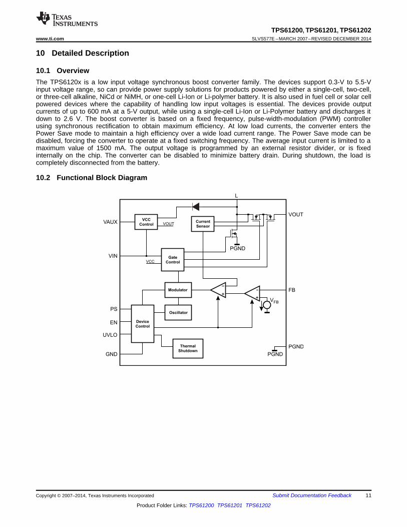
10.1 OverviewThe TPS6120x is a low input voltage synchronous boost converter family. The devices support 0.3-V to 5.5-Vinput voltage range, so can provide power supply solutions for products powered by either a single-cell, two-cell,or three-cell alkaline, NiCd or NiMH, or one-cell Li-Ion or Li-polymer battery. It is also used in fuel cell or solar cellpowered devices where the capability of handling low input voltages is essential. The devices provide outputcurrents of up to 600 mA at a 5-V output, while using a single-cell Li-Ion or Li-Polymer battery and discharges itdown to 2.6 V. The boost converter is based on a fixed frequency, pulse-width-modulation (PWM) controllerusing synchronous rectification to obtain maximum efficiency. At low load currents, the converter enters thePower Save mode to maintain a high efficiency over a wide load current range. The Power Save mode can bedisabled, forcing the converter to operate at a fixed switching frequency. The average input current is limited to amaximum value of 1500 mA. The output voltage is programmed by an external resistor divider, or is fixedinternally on the chip. The converter can be disabled to minimize battery drain. During shutdown, the load iscompletely disconnected from the battery.
10.2 Functional Block Diagram
Copyright © 2007–2014, Texas Instruments Incorporated Submit Documentation Feedback 11
Product Folder Links: TPS61200 TPS61201 TPS61202
TPS61200, TPS61201, TPS61202SLVS577E –MARCH 2007–REVISED DECEMBER 2014 www.ti.com
10.3 Feature Description
10.3.1 Controller CircuitThe controlling circuit of the device is based on an average current mode topology. The average inductor currentis regulated by a fast current regulator loop which is controlled by a voltage control loop. The controller also usesinput and output voltage feedforward. Changes of input and output voltage are monitored and immediatelychange the duty cycle in the modulator to achieve a fast response to those errors. The voltage error amplifiergets its feedback input from the FB pin. For adjustable output voltage devices, a resistive voltage divider must beconnected to that pin. For fixed output voltage devices, FB must be connected to the output voltage to directlysense the voltage. Fixed output voltage versions use a trimmed internal resistive divider. The feedback voltage iscompared with the internal reference voltage to generate a stable and accurate output voltage.
The controller circuit also senses the average input current as well as the peak input current. Thus, the maximuminput power is controlled as well as the maximum peak current, to achieve a safe and stable operation under allpossible conditions. To protect the device from overheating, an internal temperature sensor is implemented.
10.3.1.1 Synchronous OperationThe device uses three internal N-channel MOSFETs to maintain synchronous power conversion at all possibleoperating conditions. This enables the device to keep high efficiency over a wide input voltage and output powerrange.
To avoid ground shift problems due to the high currents in the switches, two separate ground pins, GND andPGND, are used. The reference for all control functions is the GND pin. The power switches are connected toPGND. Both grounds must be connected on the PCB at only one point, ideally close to the GND pin. Due to the3-switch topology, the load is always disconnected from the input during shutdown of the converter.
10.3.1.2 Down RegulationA boost converter only regulates output voltages which are higher than the input voltage. This device operatesdifferently. For example, it is able to regulate 3 V at the output with two fresh alkaline cells at the input having atotal cell voltage of 3.2 V. Another example is powering white LEDs with a forward voltage of 3.6 V from a fullycharged Li-Ion cell with an output voltage of 4.2 V. To control these applications properly, a Down Conversionmode is implemented.
If the input voltage reaches or exceeds the output voltage, the converter automatically changes to a DownConversion mode. In this mode, the control circuit changes the behavior of the two rectifying switches. Whilecontinuing switching, it sets the voltage drop across the rectifying switches as high as needed to regulate theoutput voltage. This means the power losses in the converter increase. This must be taken into account forthermal consideration.
10.3.1.3 Device EnableThe device is put into operation when EN is set high. It is put into Shutdown mode when EN is set to low. InShutdown mode, the regulator stops switching, all internal control circuitry including the UVLO comparator isswitched off, and the load is disconnected from the input. Current does not flow from input to output or fromoutput to input. This also means that the output voltage can drop below the input voltage during shutdown.
10.3.1.4 Softstart and Short-Circuit ProtectionDuring start-up of the converter, the duty cycle and the peak current are limited in order to avoid high peakcurrents drawn from the battery. After being enabled, the device starts operating. At first, it keeps the main outputVOUT disconnected, and charges the capacitor at VAUX. Once the capacitor at VAUX is charged to about 2.5 V,the device switches to normal operation. This means VOUT is turned on and the capacitor at VOUT is charged,while the load connected to the device is supplied. To ramp up the output voltage in a controlled way, theaverage current limit is set to 400 mA and rises proportional to the increase of the output voltage. At an outputvoltage of about 1.2 V the current limit is at its nominal value. If the output voltage does not increase, the currentlimit does not increase. There is no timer implemented. Thus the output voltage overshoot at startup, as well asthe inrush current, is kept at a minimum. The device ramps up the output voltage in a controlled manner even if alarge capacitor is connected at the output. When the output voltage does not increase above 1.2 V, the deviceassumes a short-circuit at the output, and keeps the current limit low to protect itself and the application. Whenthere is a short at the output during operation, the current limit is decreased accordingly.
12 Submit Documentation Feedback Copyright © 2007–2014, Texas Instruments Incorporated
Product Folder Links: TPS61200 TPS61201 TPS61202
TPS61200, TPS61201, TPS61202www.ti.com SLVS577E –MARCH 2007–REVISED DECEMBER 2014
Feature Description (continued)The device can also start into a Prebias on the outputs.
10.3.1.5 Current LimitThe device current limit limits the average current in the inductor. In a boost connector, this is the input current. Ifan excessive load requires an input current greater than the average current limit, the device limits the inputcurrent by reducing the output power delivered. In this case, the output voltage decreases.
10.3.1.6 Undervoltage LockoutAn undervoltage lockout function prevents the main output at VOUT from being supplied if the voltage at theUVLO pin drops below 0.25 V. When using a resistive divider at the voltage to be monitored, for example thesupply voltage, any threshold for the monitored voltage can be programmed. If in undervoltage lockout mode, thedevice still maintains its supply voltage at VAUX, and it is not turned off until EN is programmed low. Thisundervoltage lockout function is implemented in order to prevent the malfunctioning of the converter.
10.3.1.7 Thermal ShutdownThe device has a built-in temperature sensor which monitors the internal IC temperature. If the temperatureexceeds the programmed threshold (see electrical characteristics table), the device stops operating. As soon asthe IC temperature has decreased below the programmed threshold, it starts operating again. There is a built-inhysteresis to avoid unstable operation at IC temperatures at the thermal shutdown threshold.
10.4 Device Functional Modes
10.4.1 Power Save ModeThe Power Save (PS) pin can be used to select different operation modes. To enable Power Save mode the PSpin must be set low. Power Save mode is used to improve efficiency at light load. If Power Save mode isenabled, the converter stops operating if the average inductor current decreases below about 300 mA and theoutput voltage is at or above its nominal value. If the output voltage decreases below its nominal value, thedevice ramps up the output voltage again by starting operation using a programmed average inductor currenthigher than required by the current load condition. Operation can last for one or several pulses. The converterstops operating once the conditions for stopping operation are met again.
The Power Save mode can be disabled by programming a high at the PS pin. In Down Conversion mode, PowerSave mode is always enabled and the device cannot be forced into fixed frequency operation at light loads. ThePS input supports standard logic thresholds.
10.4.2 Down Conversion ModeIf the input voltage reaches or exceeds the output voltage, the converter automatically changes to a DownConversion mode. In this mode, the control circuit changes the behavior of the two rectifying switches. Whilecontinuing switching, it sets the voltage drop across the rectifying switches as high as needed to regulate theoutput voltage. This means the power losses in the converter increase. This must be taken into account forthermal consideration.
Copyright © 2007–2014, Texas Instruments Incorporated Submit Documentation Feedback 13
Product Folder Links: TPS61200 TPS61201 TPS61202

LVIN
EN
UVLO
PS
GND PGND
FB
VAUX
VOUT
TPS61200
VIN
VOUTC1
C2
C3
L1
R1
R2
R3
R4
TPS61200, TPS61201, TPS61202SLVS577E –MARCH 2007–REVISED DECEMBER 2014 www.ti.com
11 Application and Implementation
NOTEInformation in the following applications sections is not part of the TI componentspecification, and TI does not warrant its accuracy or completeness. TI’s customers areresponsible for determining suitability of components for their purposes. Customers shouldvalidate and test their design implementation to confirm system functionality.
11.1 Application InformationThe TPS6120x DC-DC converters are intended for systems powered by a single up to triple cell Alkaline, NiCd,NiMH battery with a typical terminal voltage between 0.7 V and 5.5 V. They can also be used in systemspowered by one-cell Li-Ion or Li-Polymer with a typical voltage between 2.5 V and 4.2 V. Additionally, any othervoltage source like solar cells or fuel cells with a typical output voltage between 0.3 V and 5.5 V can powersystems where the TPS6120x is used.
11.2 Typical Application
Figure 15. Typical Application Circuit for Adjustable Output Voltage Option
11.2.1 Design RequirementsIn this example, TPS61200 is used to design a 3.3-V power supply with 100-mA output current capability. TheTPS61200 can be powered by either a single-cell, two-cell, or three-cell alkaline, NiCd or NiMH, or one-cell Li-Ionor Li-Polymer battery. In this example, the input voltage range is from 0.8 V to 1.65 V for single-cell alkalineinput.
11.2.2 Detailed Design Procedure
Table 2. List of ComponentsCOMPONENT REFERENCE PART NUMBER MANUFACTURER VALUEC1 any 10 μF, X7R CeramicC2 any 2 x 10 μF, X7R CeramicC3 any 1 µF, X7R, CeramicL1 LPS3015-222ML Coilcraft 2.2 μH
11.2.2.1 Programming the Output Voltage
Within the TPS6120X family, there are fixed and adjustable output voltage versions available. To properlyconfigure the fixed output voltage devices, the FB pin is used to sense the output voltage. This means that itmust be connected directly to VOUT. For the adjustable output voltage version, an external resistor divider isused to adjust the output voltage. The resistor divider must be connected between VOUT, FB and GND. Whenthe output voltage is regulated properly, the typical value of the voltage at the FB pin is 500 mV. The maximumrecommended value for the output voltage is 5.5 V. The current through the resistive divider should be about 100times greater than the current into the FB pin. The typical current into the FB pin is 0.01 μA, and the voltage
14 Submit Documentation Feedback Copyright © 2007–2014, Texas Instruments Incorporated
Product Folder Links: TPS61200 TPS61201 TPS61202
( )IN OUT INOUT OUTLMAX
IN OUT
V x V VV x II = +
0.8 x V 2 x V x f x L
-
MIN IN
sL = V x 0.5
A
m
INMIN
UVLO
VR3 = R4 x - 1
V
æ öç ÷ç ÷è ø
OUT
FB
VR1 = R2 x - 1
V
æ öç ÷è ø
TPS61200, TPS61201, TPS61202www.ti.com SLVS577E –MARCH 2007–REVISED DECEMBER 2014
across the resistor between FB and GND, R2, is typically 500 mV. Based on those two values, therecommended value for R2 should be lower than 500 kΩ, in order to set the divider current at 1 μA or higher. It isrecommended to keep the value for this resistor in the range of 200 kΩ. The value of the resistor connectedbetween VOUT and FB, R1, depending on the needed output voltage (VOUT), can be calculated usingEquation 1:
(1)
As an example, for an output voltage of 3.3 V, a 1-MΩ resistor should be chosen for R1 when a 180-kΩ isselected for R2.
11.2.2.2 Programming the UVLO Threshold VoltageThe UVLO input can be used to shut down the main output if the supply voltage is getting too low. The internalreference threshold is typically 250 mV. If the supply voltage should cause the shutdown when it is droppingbelow 250 mV, VIN can be connected directly to the UVLO pin. If the shutdown should happen at higher voltages,a resistor divider can be used. R3 and R4 in Figure 15 show an example of how to monitor the input voltage ofthe circuit. The current through the resistive divider should be about 100 times greater than the current into theUVLO pin. The typical current into the UVLO pin is 0.01 μA, and the voltage across R4 is equal to the UVLOvoltage threshold that is generated on-chip, which has a value of 250 mV. Therefore, the recommended value forR4 is in the range of 250 kΩ. From this, the value of resistor R3, depending on the desired shutdown voltageVINMIN, can be calculated using Equation 2.
(2)
11.2.2.3 Inductor SelectionTo make sure that the TPS6120X devices can operate, an inductor must be connected between the VIN and Lpins. To estimate the minimum inductance value, Equation 3 can be used.
(3)
In Equation 3, the minimum inductance, LMIN , for boost mode operation is calculated. VIN is the maximum inputvoltage. The recommended inductor value range is between 1.5 μH and 4.7 μH. The minimum inductor valueshould not be below 1.5 μH, even if Equation 3 yields something lower. Using 2.2 μH is recommended anywayfor getting best performance over the whole input and output voltage range.
With the chosen inductance value, the peak current for the inductor in steady state operation can be calculatedusing Equation 4.
(4)
This would be the critical value for the current rating for selecting the inductor. It also needs to be taken intoaccount that load transients and error conditions may cause higher inductor currents. The following inductorseries from different suppliers have been used with TPS6120x converters:
Table 3. List of InductorsVENDOR INDUCTOR SERIES
LPS3015Coilcraft
LPS4012Murata LQH3NPTajo Yuden NR3015Wurth Elektronik WE-TPC Typ S
Copyright © 2007–2014, Texas Instruments Incorporated Submit Documentation Feedback 15
Product Folder Links: TPS61200 TPS61201 TPS61202

OUT
FC = 5 x L x
H
m
m
TPS61200, TPS61201, TPS61202SLVS577E –MARCH 2007–REVISED DECEMBER 2014 www.ti.com
11.2.2.4 Capacitor Selection
11.2.2.4.1 Input Capacitor
At least a 4.7-μF input capacitor is recommended to improve transient behavior of the regulator and EMIbehavior of the total power supply circuit. An X5R or X7R ceramic capacitor placed as close as possible to theVIN and PGND pins of the IC is recommended.
An R-C filter may be placed on the VIN pin to improve performance in applications with a noisy input source. A100-Ω resistor and 0.1-µF capacitor are recommended in this case. This filter is not required operation.
11.2.2.4.2 Output Capacitor
For the output capacitor, it is recommended to use small X5R or X7R ceramic capacitors placed as close aspossible to the VOUT and PGND pins of the IC. If, for any reason, the application requires the use of largecapacitors which can not be placed close to the IC, using a smaller ceramic capacitor in parallel to the large oneis required. This small capacitor should be placed as close as possible to the VOUT and PGND pins of the IC.
To get an estimate of the recommended minimum output capacitance, Equation 5 can be used.
(5)
A capacitor with a value in the range of the calculated minimum should be used. This is required to maintaincontrol loop stability. There are no additional requirements regarding minimum ESR. There is also no upper limitfor the output capacitance value. Larger capacitors cause lower output voltage ripple as well as lower outputvoltage drops during load transients.
11.2.2.4.3 Capacitor at VAUX
Between the VAUX pin and GND pin, a capacitor must be connected. This capacitor is used to maintain and filterthe control supply voltage, which is chosen from the highest of VIN, VOUT, and L. It is charged during startupand before the main output VOUT is turned on. To ensure stable operation, using at least 0.1μF isrecommended. At output voltages below 2.5 V, the capacitance should be in the range of 1 μF. Since thiscapacitor is also used as a snubber capacitor for the main switch, using a X5R or X7R ceramic capacitor withlow ESR is important.
11.2.3 Application Curves
FIGUREOutput Voltage TPS61201, Power Save Mode Disabled Figure 16Output Voltage TPS61202, Power Save Mode Disabled Figure 17Output Voltage TPS61201, Power Save Mode Enabled Figure 18Output Voltage TPS61202, Power Save Mode Enabled Figure 19TPS61201 Load Transient Response Figure 20TPS61202 Load Transient Response Figure 21TPS61201 Line Transient Response Figure 22TPS61202 Line Transient Response Figure 23TPS61201 Startup after Enable Figure 24TPS61202 Startup after Enable Figure 25
16 Submit Documentation Feedback Copyright © 2007–2014, Texas Instruments Incorporated
Product Folder Links: TPS61200 TPS61201 TPS61202

t - Time - 1 ms/div
TPS61201V = 3.3 VO
V = 1.8 V, I = 300 mA to 400 mAI L
Ou
tpu
t V
olt
ag
e5
0 m
V/d
iv,A
CO
utp
ut
Cu
rre
nt
50
mA
/div
,A
C
t - Time - 1 ms/div
TPS61202V = 5 VO
V = 1.8 V, I = 150 mA to 250 mAI L
Ou
tpu
t V
olt
ag
e100 m
V/d
iv,A
CO
utp
ut
Cu
rren
t100 m
A/d
iv,A
C
t - Time - 100 s/divm
TPS61202V = 5 V,
Power Save EnabledO
V = 1.8 V, R = 55 kI L W
Ou
tpu
t V
olt
ag
e20 m
V/d
iv,A
CIn
du
cto
r C
urr
en
t200 m
A/d
iv
t - Time - 2 ms/div
TPS61201V = 3.3 V,
Power Save EnabledO
V = 1.8 V, R = 33 kI L W
Ou
tpu
t V
olt
ag
e2
0 m
V/d
iv,A
CIn
du
cto
r C
urr
en
t1
00
mA
/div
t - Time - 1 s/divm
TPS61202V = 5 V,
Power Save DisabledO
V = 1.8 V, R = 17I L W
Ou
tpu
t V
olt
ag
e5
0 m
V/d
iv,A
CIn
du
cto
r C
urr
en
t2
00
mA
/div
,A
C
t - Time - 0.5 s/divm
TPS61201V = 3.3 V,
Power Save DisabledO
V = 1.8 V, R = 11I L W
Ou
tpu
t V
olt
ag
e20 m
V/d
iv,A
CIn
du
cto
r C
urr
en
t100 m
A/d
iv,A
C
TPS61200, TPS61201, TPS61202www.ti.com SLVS577E –MARCH 2007–REVISED DECEMBER 2014
Figure 16. Output Voltage, Power Save Mode Disabled Figure 17. Output Voltage, Power Save Mode Disabled
Figure 18. Output Voltage in Power Save Mode Figure 19. Output Voltage in Power Save Mode
Figure 21. Load Transient ResponseFigure 20. Load Transient Response
Copyright © 2007–2014, Texas Instruments Incorporated Submit Documentation Feedback 17
Product Folder Links: TPS61200 TPS61201 TPS61202

t - Time - 100 s/divm
TPS61201V = 3.3 VO
V = 1.8 V, R = 17I L W
Voltage at L 2 V/div, DC
Inductor Current 500 mA/div, DC
Enable 5 V/div, DCVoltage at VAUX 2 V/div, DC
Output Voltage 2 V/div, DC
t - Time - 100 s/divm
TPS61201V = 3.3 VO
V = 1.8 V, R = 11I L W
Voltage at L 2 V/div, DC
Inductor Current 500 mA/div, DC
Enable 5 V/div, DC
Voltage at VAUX 2 V/div, DC
Output Voltage 2 V/div, DC
t - Time - 2 ms/div
TPS61201V = 3.3 VO
V = 1.8 V to 2.4 V, R = 11I L W
Inp
ut
Vo
lta
ge
50
0 m
V/d
iv,A
CO
utp
ut
Vo
lta
ge
50
mV
/div
,A
C
t - Time - 2 ms/div
TPS61202V = 5 VO
V = 3 V to 3.6 V, R = 17I L W
Inp
ut
Vo
lta
ge
50
0 m
V/d
iv,A
CO
utp
ut
Vo
lta
ge
20
mV
/div
,A
C
TPS61200, TPS61201, TPS61202SLVS577E –MARCH 2007–REVISED DECEMBER 2014 www.ti.com
Figure 23. Line Transient ResponseFigure 22. Line Transient Response
Figure 24. Start-Up After Enable Figure 25. Start-Up After Enable
18 Submit Documentation Feedback Copyright © 2007–2014, Texas Instruments Incorporated
Product Folder Links: TPS61200 TPS61201 TPS61202

VIN
EN
UVLO
PS
GND
L
VOUT
FB
VAUX
PGND
TP
S61200
V = 0.3 - 0.5Vcell
VOUT
Sola
r C
ell
L1 4.7µH
R2
CFFC1
C3
R1
R5
C5
R6
R3
R7
R4 OPA379
C2
TLV431
R8
C4
MPP circuit
VCELL
Chargestoragedevice
VCELL
VAUX
VAUX
Power ground
Reference ground
VAUX
RefDes Value
C1 >10 F
C2 >20 F
C3 1 F
C4 1 FC5 10 nFC 33 pF
L1 4.7 H
m
m
m
m
m
FF
RefDes Value
R1 750 k
R2 200 k
R3 1 k
R4 1 M
R5 100
R6 1 M
R7 100 k
R8 200 k
W
W
W
W
W
W
W
W
TPS61200, TPS61201, TPS61202www.ti.com SLVS577E –MARCH 2007–REVISED DECEMBER 2014
11.3 System Examples
Figure 26. WLED Driver Circuit (See SLVA364)
Figure 27. Solar Cell Circuit (See SLVA345)
Copyright © 2007–2014, Texas Instruments Incorporated Submit Documentation Feedback 19
Product Folder Links: TPS61200 TPS61201 TPS61202

1Vaux
2Vout
3L
4PGND
5VIN
10FB
9GND
8PS
7UVLO
6EN
TPS61200
TPS61200
10uFC1
Q1MOSFET-N
100
R1
L1
Inductor2.2uH
1K
R3
0
R2
100nF
C2
1K
R4
1K
R5
47uFC3
10uFC4
Battery
Vin
Vout
GND
0.9V to 1.5V
3.3V
TPS61200, TPS61201, TPS61202SLVS577E –MARCH 2007–REVISED DECEMBER 2014 www.ti.com
System Examples (continued)
Figure 28. Reverse Battery Protection Circuit (See SLVA315)
12 Power Supply RecommendationsThe power supply of TPS6120x DC-DC converters can be a single up to triple cell Alkaline, NiCd, NiMH batterywith a typical terminal voltage between 0.7 V and 5.5 V. The TPS6120x can also be powered by one-cell Li-Ionor Li-Polymer with a typical voltage between 2.5 V and 4.2 V. Additionally, any other voltage source like solarcells or fuel cells with a typical output voltage between 0.3 V and 5.5 V can also be the power supply.
The input supply should be well regulated with the rating of TPS6120x. If the input supply is located more than afew inches from the device, additional bulk capacitance may be required in addition to the ceramic bypasscapacitors. An electrolytic or tantalum capacitor with a value of 47 µF is a typical choice.
20 Submit Documentation Feedback Copyright © 2007–2014, Texas Instruments Incorporated
Product Folder Links: TPS61200 TPS61201 TPS61202

J(MAX) AD(MAX)
JA
T T 125 C 85 CP 971mW
R 41.2 C / Wq
- ° - °= = =
°
TPS61200, TPS61201, TPS61202www.ti.com SLVS577E –MARCH 2007–REVISED DECEMBER 2014
13 Layout
13.1 Layout GuidelinesAs for all switching power supplies, the layout is an important step in the design, especially at high peak currentsand high switching frequencies. If the layout is not carefully done, the regulator could show stability problems aswell as EMI problems. Therefore, use wide and short traces for the main current path and for the power groundtracks. The input and output capacitor, as well as the inductor should be placed as close as possible to the IC.Use a common ground node for power ground and a different one for control ground to minimize the effects ofground noise. Connect these ground nodes at any place close to one of the ground pins of the IC.
The feedback divider should be placed as close as possible to the control ground pin of the IC. To lay out thecontrol ground, it is recommended to use short traces as well, separated from the power ground traces. Thisavoids ground shift problems, which can occur due to superimposition of power ground current and controlground current. See Figure 29 for the recommended layout.
13.2 Layout Example
Figure 29. EVM Layout
13.3 Thermal ConsiderationsImplementation of integrated circuits in low-profile and fine-pitch surface-mount packages typically requiresspecial attention to power dissipation. Many system-dependent issues such as thermal coupling, airflow, addedheat sinks and convection surfaces, and the presence of other heat-generating components affect the power-dissipation limits of a given component.
Three basic approaches for enhancing thermal performance are listed below.• Improving the power dissipation capability of the PCB design• Improving the thermal coupling of the component to the PCB• Introducing airflow in the system
The maximum recommended junction temperature (TJ) of the TPS6120x devices is 125°C. The thermalresistance of the 10-pin SON 3 × 3 package (DRC) is RθJA = 41.2 °C/W, when the exposed thermal pad issoldered. Specified regulator operation is assured to a maximum ambient temperature, TA, of 85°C. Therefore,the maximum power dissipation is about 971 mW. More power can be dissipated if the maximum ambienttemperature of the application is lower.
(6)
Copyright © 2007–2014, Texas Instruments Incorporated Submit Documentation Feedback 21
Product Folder Links: TPS61200 TPS61201 TPS61202

TPS61200, TPS61201, TPS61202SLVS577E –MARCH 2007–REVISED DECEMBER 2014 www.ti.com
14 Device and Documentation Support
14.1 Related LinksThe table below lists quick access links. Categories include technical documents, support and communityresources, tools and software, and quick access to sample or buy.
Table 4. Related LinksTECHNICAL TOOLS & SUPPORT &PARTS PRODUCT FOLDER SAMPLE & BUY DOCUMENTS SOFTWARE COMMUNITY
TPS61200 Click here Click here Click here Click here Click hereTPS61201 Click here Click here Click here Click here Click hereTPS61202 Click here Click here Click here Click here Click here
14.2 TrademarksAll trademarks are the property of their respective owners.
14.3 Electrostatic Discharge CautionThese devices have limited built-in ESD protection. The leads should be shorted together or the device placed in conductive foamduring storage or handling to prevent electrostatic damage to the MOS gates.
14.4 GlossarySLYZ022 — TI Glossary.
This glossary lists and explains terms, acronyms, and definitions.
15 Mechanical, Packaging, and Orderable InformationThe following pages include mechanical, packaging, and orderable information. This information is the mostcurrent data available for the designated devices. This data is subject to change without notice and revision ofthis document. For browser-based versions of this data sheet, refer to the left-hand navigation.
22 Submit Documentation Feedback Copyright © 2007–2014, Texas Instruments Incorporated
Product Folder Links: TPS61200 TPS61201 TPS61202

PACKAGE OPTION ADDENDUM
www.ti.com 30-Sep-2014
Addendum-Page 1
PACKAGING INFORMATION
Orderable Device Status(1)
Package Type PackageDrawing
Pins PackageQty
Eco Plan(2)
Lead/Ball Finish(6)
MSL Peak Temp(3)
Op Temp (°C) Device Marking(4/5)
Samples
TPS61200DRCR ACTIVE VSON DRC 10 3000 Green (RoHS& no Sb/Br)
CU NIPDAU Level-2-260C-1 YEAR -40 to 85 BRR
TPS61200DRCRG4 ACTIVE VSON DRC 10 3000 Green (RoHS& no Sb/Br)
CU NIPDAU Level-2-260C-1 YEAR -40 to 85 BRR
TPS61200DRCT ACTIVE VSON DRC 10 250 Green (RoHS& no Sb/Br)
CU NIPDAU Level-2-260C-1 YEAR -40 to 85 BRR
TPS61200DRCTG4 ACTIVE VSON DRC 10 250 Green (RoHS& no Sb/Br)
CU NIPDAU Level-2-260C-1 YEAR -40 to 85 BRR
TPS61201DRCR ACTIVE VSON DRC 10 3000 Green (RoHS& no Sb/Br)
CU NIPDAU Level-2-260C-1 YEAR -40 to 85 BRS
TPS61201DRCRG4 ACTIVE VSON DRC 10 3000 Green (RoHS& no Sb/Br)
CU NIPDAU Level-2-260C-1 YEAR -40 to 85 BRS
TPS61201DRCT ACTIVE VSON DRC 10 250 Green (RoHS& no Sb/Br)
CU NIPDAU Level-2-260C-1 YEAR -40 to 85 BRS
TPS61201DRCTG4 ACTIVE VSON DRC 10 250 Green (RoHS& no Sb/Br)
CU NIPDAU Level-2-260C-1 YEAR -40 to 85 BRS
TPS61202DRCR ACTIVE VSON DRC 10 3000 Green (RoHS& no Sb/Br)
CU NIPDAU Level-2-260C-1 YEAR -40 to 85 BRT
TPS61202DRCT ACTIVE VSON DRC 10 250 Green (RoHS& no Sb/Br)
CU NIPDAU Level-2-260C-1 YEAR -40 to 85 BRT
TPS61202DRCTG4 ACTIVE VSON DRC 10 250 Green (RoHS& no Sb/Br)
CU NIPDAU Level-2-260C-1 YEAR -40 to 85 BRT
TPS61202DSCR ACTIVE WSON DSC 10 3000 Green (RoHS& no Sb/Br)
CU NIPDAU Level-2-260C-1 YEAR -40 to 85 CER
TPS61202DSCT ACTIVE WSON DSC 10 250 Green (RoHS& no Sb/Br)
CU NIPDAU Level-2-260C-1 YEAR -40 to 85 CER
TPS61202DSCTG4 ACTIVE WSON DSC 10 250 Green (RoHS& no Sb/Br)
CU NIPDAU Level-2-260C-1 YEAR -40 to 85 CER
(1) The marketing status values are defined as follows:ACTIVE: Product device recommended for new designs.LIFEBUY: TI has announced that the device will be discontinued, and a lifetime-buy period is in effect.NRND: Not recommended for new designs. Device is in production to support existing customers, but TI does not recommend using this part in a new design.PREVIEW: Device has been announced but is not in production. Samples may or may not be available.OBSOLETE: TI has discontinued the production of the device.

PACKAGE OPTION ADDENDUM
www.ti.com 30-Sep-2014
Addendum-Page 2
(2) Eco Plan - The planned eco-friendly classification: Pb-Free (RoHS), Pb-Free (RoHS Exempt), or Green (RoHS & no Sb/Br) - please check http://www.ti.com/productcontent for the latest availabilityinformation and additional product content details.TBD: The Pb-Free/Green conversion plan has not been defined.Pb-Free (RoHS): TI's terms "Lead-Free" or "Pb-Free" mean semiconductor products that are compatible with the current RoHS requirements for all 6 substances, including the requirement thatlead not exceed 0.1% by weight in homogeneous materials. Where designed to be soldered at high temperatures, TI Pb-Free products are suitable for use in specified lead-free processes.Pb-Free (RoHS Exempt): This component has a RoHS exemption for either 1) lead-based flip-chip solder bumps used between the die and package, or 2) lead-based die adhesive used betweenthe die and leadframe. The component is otherwise considered Pb-Free (RoHS compatible) as defined above.Green (RoHS & no Sb/Br): TI defines "Green" to mean Pb-Free (RoHS compatible), and free of Bromine (Br) and Antimony (Sb) based flame retardants (Br or Sb do not exceed 0.1% by weightin homogeneous material)
(3) MSL, Peak Temp. - The Moisture Sensitivity Level rating according to the JEDEC industry standard classifications, and peak solder temperature.
(4) There may be additional marking, which relates to the logo, the lot trace code information, or the environmental category on the device.
(5) Multiple Device Markings will be inside parentheses. Only one Device Marking contained in parentheses and separated by a "~" will appear on a device. If a line is indented then it is a continuationof the previous line and the two combined represent the entire Device Marking for that device.
(6) Lead/Ball Finish - Orderable Devices may have multiple material finish options. Finish options are separated by a vertical ruled line. Lead/Ball Finish values may wrap to two lines if the finishvalue exceeds the maximum column width.
Important Information and Disclaimer:The information provided on this page represents TI's knowledge and belief as of the date that it is provided. TI bases its knowledge and belief on informationprovided by third parties, and makes no representation or warranty as to the accuracy of such information. Efforts are underway to better integrate information from third parties. TI has taken andcontinues to take reasonable steps to provide representative and accurate information but may not have conducted destructive testing or chemical analysis on incoming materials and chemicals.TI and TI suppliers consider certain information to be proprietary, and thus CAS numbers and other limited information may not be available for release.
In no event shall TI's liability arising out of such information exceed the total purchase price of the TI part(s) at issue in this document sold by TI to Customer on an annual basis.
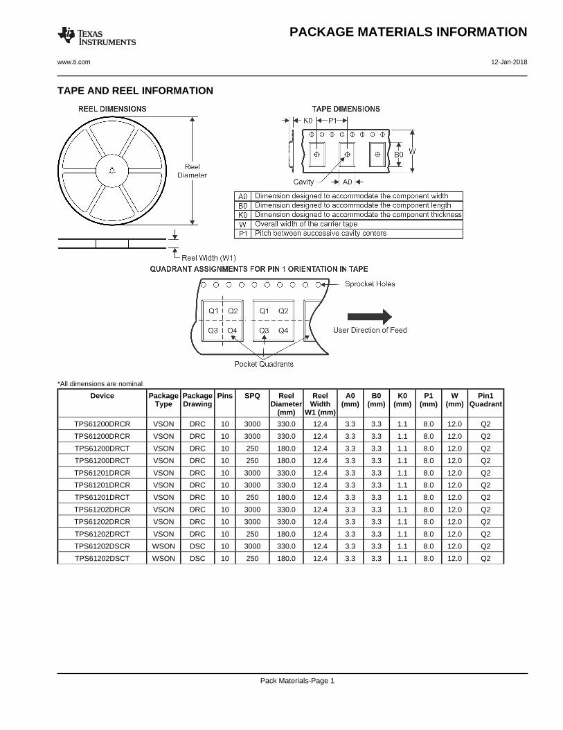
TAPE AND REEL INFORMATION
*All dimensions are nominal
Device PackageType
PackageDrawing
Pins SPQ ReelDiameter
(mm)
ReelWidth
W1 (mm)
A0(mm)
B0(mm)
K0(mm)
P1(mm)
W(mm)
Pin1Quadrant
TPS61200DRCR VSON DRC 10 3000 330.0 12.4 3.3 3.3 1.1 8.0 12.0 Q2
TPS61200DRCR VSON DRC 10 3000 330.0 12.4 3.3 3.3 1.1 8.0 12.0 Q2
TPS61200DRCT VSON DRC 10 250 180.0 12.4 3.3 3.3 1.1 8.0 12.0 Q2
TPS61200DRCT VSON DRC 10 250 180.0 12.4 3.3 3.3 1.1 8.0 12.0 Q2
TPS61201DRCR VSON DRC 10 3000 330.0 12.4 3.3 3.3 1.1 8.0 12.0 Q2
TPS61201DRCR VSON DRC 10 3000 330.0 12.4 3.3 3.3 1.1 8.0 12.0 Q2
TPS61201DRCT VSON DRC 10 250 180.0 12.4 3.3 3.3 1.1 8.0 12.0 Q2
TPS61202DRCR VSON DRC 10 3000 330.0 12.4 3.3 3.3 1.1 8.0 12.0 Q2
TPS61202DRCR VSON DRC 10 3000 330.0 12.4 3.3 3.3 1.1 8.0 12.0 Q2
TPS61202DRCT VSON DRC 10 250 180.0 12.4 3.3 3.3 1.1 8.0 12.0 Q2
TPS61202DSCR WSON DSC 10 3000 330.0 12.4 3.3 3.3 1.1 8.0 12.0 Q2
TPS61202DSCT WSON DSC 10 250 180.0 12.4 3.3 3.3 1.1 8.0 12.0 Q2
PACKAGE MATERIALS INFORMATION
www.ti.com 12-Jan-2018
Pack Materials-Page 1
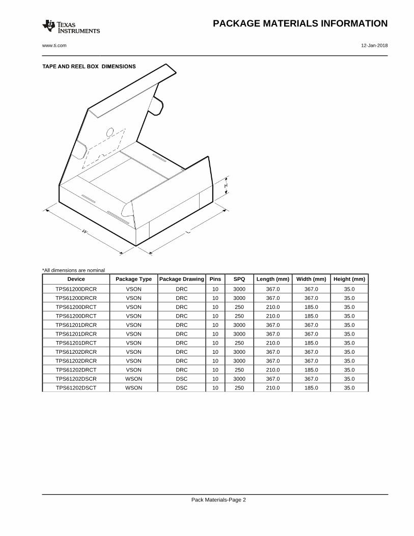
*All dimensions are nominal
Device Package Type Package Drawing Pins SPQ Length (mm) Width (mm) Height (mm)
TPS61200DRCR VSON DRC 10 3000 367.0 367.0 35.0
TPS61200DRCR VSON DRC 10 3000 367.0 367.0 35.0
TPS61200DRCT VSON DRC 10 250 210.0 185.0 35.0
TPS61200DRCT VSON DRC 10 250 210.0 185.0 35.0
TPS61201DRCR VSON DRC 10 3000 367.0 367.0 35.0
TPS61201DRCR VSON DRC 10 3000 367.0 367.0 35.0
TPS61201DRCT VSON DRC 10 250 210.0 185.0 35.0
TPS61202DRCR VSON DRC 10 3000 367.0 367.0 35.0
TPS61202DRCR VSON DRC 10 3000 367.0 367.0 35.0
TPS61202DRCT VSON DRC 10 250 210.0 185.0 35.0
TPS61202DSCR WSON DSC 10 3000 367.0 367.0 35.0
TPS61202DSCT WSON DSC 10 250 210.0 185.0 35.0
PACKAGE MATERIALS INFORMATION
www.ti.com 12-Jan-2018
Pack Materials-Page 2

GENERIC PACKAGE VIEW
Images above are just a representation of the package family, actual package may vary.Refer to the product data sheet for package details.
DRC 10 VSON - 1 mm max heightPLASTIC SMALL OUTLINE - NO LEAD
4204102-3/M
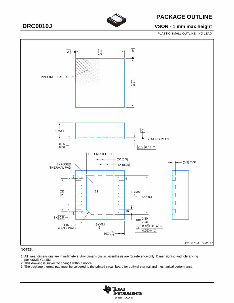
www.ti.com
PACKAGE OUTLINE
C
10X 0.300.18
2.4 0.1
2X2
1.65 0.1
8X 0.5
1 MAX
10X 0.50.3
0.050.00
A 3.12.9
B
3.12.9
(0.2) TYP4X (0.25)
2X (0.5)
VSON - 1 mm max heightDRC0010JPLASTIC SMALL OUTLINE - NO LEAD
4218878/A 09/2017
PIN 1 INDEX AREA
SEATING PLANE
0.08 C
1
56
10
(OPTIONAL)PIN 1 ID 0.1 C A B
0.05 C
THERMAL PADEXPOSED
SYMM
SYMM11
NOTES: 1. All linear dimensions are in millimeters. Any dimensions in parenthesis are for reference only. Dimensioning and tolerancing per ASME Y14.5M. 2. This drawing is subject to change without notice. 3. The package thermal pad must be soldered to the printed circuit board for optimal thermal and mechanical performance.
SCALE 4.000

www.ti.com
EXAMPLE BOARD LAYOUT
0.07 MINALL AROUND
10X (0.25)
(2.4)
(2.8)
8X (0.5)
(1.65)
( 0.2) VIATYP
(0.575)
(0.95)
10X (0.6)
(R0.05) TYP
(3.4)
4X (0.25)
(0.5)
VSON - 1 mm max heightDRC0010JPLASTIC SMALL OUTLINE - NO LEAD
4218878/A 09/2017
SYMM
1
5 6
10
LAND PATTERN EXAMPLEEXPOSED METAL SHOWN
SCALE:20X
11SYMM
METAL UNDERSOLDER MASK
SOLDER MASKOPENING
NOTES: (continued) 4. This package is designed to be soldered to a thermal pad on the board. For more information, see Texas Instruments literature number SLUA271 (www.ti.com/lit/slua271).5. Vias are optional depending on application, refer to device data sheet. If any vias are implemented, refer to their locations shown on this view. It is recommended that vias under paste be filled, plugged or tented.
www.ti.com
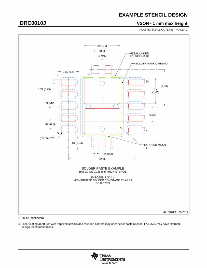
EXAMPLE STENCIL DESIGN
(R0.05) TYP
10X (0.25)
10X (0.6)
2X (1.5)
2X(1.06)
(2.8)
(0.63)
8X (0.5)
(0.5)
4X (0.34)
4X (0.25)
(1.53)
VSON - 1 mm max heightDRC0010JPLASTIC SMALL OUTLINE - NO LEAD
4218878/A 09/2017
NOTES: (continued) 6. Laser cutting apertures with trapezoidal walls and rounded corners may offer better paste release. IPC-7525 may have alternate design recommendations.
SOLDER PASTE EXAMPLEBASED ON 0.125 mm THICK STENCIL
EXPOSED PAD 11:
80% PRINTED SOLDER COVERAGE BY AREASCALE:25X
SYMM
1
56
10
EXPOSED METALTYP
11
SYMM
SOLDER MASK OPENING
METAL UNDERSOLDER MASK


www.ti.com
PACKAGE OUTLINE
C
10X 0.300.18
2.4 0.1
2X2
1.65 0.1
8X 0.5
10X 0.50.3
0.050.00
0.8 MAX
A 3.12.9
B
3.12.9
(0.2) TYP4X (0.25)
2X (0.5)
WSON - 0.8 mm max heightDSC0010JPLASTIC SMALL OUTLINE - NO LEAD
4221826/C 12/2017
PIN 1 INDEX AREA
SEATING PLANE
0.08 C
1
56
10
(OPTIONAL)PIN 1 ID 0.1 C A B
0.05 C
THERMAL PADEXPOSED
SYMM
SYMM11
NOTES: 1. All linear dimensions are in millimeters. Any dimensions in parenthesis are for reference only. Dimensioning and tolerancing per ASME Y14.5M. 2. This drawing is subject to change without notice. 3. The package thermal pad must be soldered to the printed circuit board for optimal thermal and mechanical performance.
SCALE 4.000

www.ti.com
EXAMPLE BOARD LAYOUT
0.07 MINALL AROUND
10X (0.25)
(2.4)
(2.8)
8X (0.5)
(1.65)
( 0.2) VIATYP
(0.575)
(0.95)
10X (0.6)
(R0.05) TYP
(3.4)
4X (0.25)
(0.5)
WSON - 0.8 mm max heightDSC0010JPLASTIC SMALL OUTLINE - NO LEAD
4221826/C 12/2017
SYMM
1
5 6
10
LAND PATTERN EXAMPLESOLDER MASK DEFINED
EXPOSED METAL SHOWNSCALE:20X
11SYMM
METAL UNDERSOLDER MASK
SOLDER MASKOPENING
NOTES: (continued) 4. This package is designed to be soldered to a thermal pad on the board. For more information, see Texas Instruments literature number SLUA271 (www.ti.com/lit/slua271).5. Vias are optional depending on application, refer to device data sheet. If any vias are implemented, refer to their locations shown on this view. It is recommended that vias under paste be filled, plugged or tented.

www.ti.com
EXAMPLE STENCIL DESIGN
(R0.05) TYP
10X (0.25)
10X (0.6)
2X (1.5)
2X(1.06)
(2.8)
(0.63)
8X (0.5)
(0.5)
4X (0.34)
4X (0.25)
(1.53)
WSON - 0.8 mm max heightDSC0010JPLASTIC SMALL OUTLINE - NO LEAD
4221826/C 12/2017
NOTES: (continued) 6. Laser cutting apertures with trapezoidal walls and rounded corners may offer better paste release. IPC-7525 may have alternate design recommendations.
SOLDER PASTE EXAMPLEBASED ON 0.125 mm THICK STENCIL
EXPOSED PAD 11:
80% PRINTED SOLDER COVERAGE BY AREASCALE:25X
SYMM
1
56
10
EXPOSED METALTYP
11
SYMM
SOLDER MASK OPENING
METAL UNDERSOLDER MASK
IMPORTANT NOTICE
Texas Instruments Incorporated (TI) reserves the right to make corrections, enhancements, improvements and other changes to itssemiconductor products and services per JESD46, latest issue, and to discontinue any product or service per JESD48, latest issue. Buyersshould obtain the latest relevant information before placing orders and should verify that such information is current and complete.TI’s published terms of sale for semiconductor products (http://www.ti.com/sc/docs/stdterms.htm) apply to the sale of packaged integratedcircuit products that TI has qualified and released to market. Additional terms may apply to the use or sale of other types of TI products andservices.Reproduction of significant portions of TI information in TI data sheets is permissible only if reproduction is without alteration and isaccompanied by all associated warranties, conditions, limitations, and notices. TI is not responsible or liable for such reproduceddocumentation. Information of third parties may be subject to additional restrictions. Resale of TI products or services with statementsdifferent from or beyond the parameters stated by TI for that product or service voids all express and any implied warranties for theassociated TI product or service and is an unfair and deceptive business practice. TI is not responsible or liable for any such statements.Buyers and others who are developing systems that incorporate TI products (collectively, “Designers”) understand and agree that Designersremain responsible for using their independent analysis, evaluation and judgment in designing their applications and that Designers havefull and exclusive responsibility to assure the safety of Designers' applications and compliance of their applications (and of all TI productsused in or for Designers’ applications) with all applicable regulations, laws and other applicable requirements. Designer represents that, withrespect to their applications, Designer has all the necessary expertise to create and implement safeguards that (1) anticipate dangerousconsequences of failures, (2) monitor failures and their consequences, and (3) lessen the likelihood of failures that might cause harm andtake appropriate actions. Designer agrees that prior to using or distributing any applications that include TI products, Designer willthoroughly test such applications and the functionality of such TI products as used in such applications.TI’s provision of technical, application or other design advice, quality characterization, reliability data or other services or information,including, but not limited to, reference designs and materials relating to evaluation modules, (collectively, “TI Resources”) are intended toassist designers who are developing applications that incorporate TI products; by downloading, accessing or using TI Resources in anyway, Designer (individually or, if Designer is acting on behalf of a company, Designer’s company) agrees to use any particular TI Resourcesolely for this purpose and subject to the terms of this Notice.TI’s provision of TI Resources does not expand or otherwise alter TI’s applicable published warranties or warranty disclaimers for TIproducts, and no additional obligations or liabilities arise from TI providing such TI Resources. TI reserves the right to make corrections,enhancements, improvements and other changes to its TI Resources. TI has not conducted any testing other than that specificallydescribed in the published documentation for a particular TI Resource.Designer is authorized to use, copy and modify any individual TI Resource only in connection with the development of applications thatinclude the TI product(s) identified in such TI Resource. NO OTHER LICENSE, EXPRESS OR IMPLIED, BY ESTOPPEL OR OTHERWISETO ANY OTHER TI INTELLECTUAL PROPERTY RIGHT, AND NO LICENSE TO ANY TECHNOLOGY OR INTELLECTUAL PROPERTYRIGHT OF TI OR ANY THIRD PARTY IS GRANTED HEREIN, including but not limited to any patent right, copyright, mask work right, orother intellectual property right relating to any combination, machine, or process in which TI products or services are used. Informationregarding or referencing third-party products or services does not constitute a license to use such products or services, or a warranty orendorsement thereof. Use of TI Resources may require a license from a third party under the patents or other intellectual property of thethird party, or a license from TI under the patents or other intellectual property of TI.TI RESOURCES ARE PROVIDED “AS IS” AND WITH ALL FAULTS. TI DISCLAIMS ALL OTHER WARRANTIES ORREPRESENTATIONS, EXPRESS OR IMPLIED, REGARDING RESOURCES OR USE THEREOF, INCLUDING BUT NOT LIMITED TOACCURACY OR COMPLETENESS, TITLE, ANY EPIDEMIC FAILURE WARRANTY AND ANY IMPLIED WARRANTIES OFMERCHANTABILITY, FITNESS FOR A PARTICULAR PURPOSE, AND NON-INFRINGEMENT OF ANY THIRD PARTY INTELLECTUALPROPERTY RIGHTS. TI SHALL NOT BE LIABLE FOR AND SHALL NOT DEFEND OR INDEMNIFY DESIGNER AGAINST ANY CLAIM,INCLUDING BUT NOT LIMITED TO ANY INFRINGEMENT CLAIM THAT RELATES TO OR IS BASED ON ANY COMBINATION OFPRODUCTS EVEN IF DESCRIBED IN TI RESOURCES OR OTHERWISE. IN NO EVENT SHALL TI BE LIABLE FOR ANY ACTUAL,DIRECT, SPECIAL, COLLATERAL, INDIRECT, PUNITIVE, INCIDENTAL, CONSEQUENTIAL OR EXEMPLARY DAMAGES INCONNECTION WITH OR ARISING OUT OF TI RESOURCES OR USE THEREOF, AND REGARDLESS OF WHETHER TI HAS BEENADVISED OF THE POSSIBILITY OF SUCH DAMAGES.Unless TI has explicitly designated an individual product as meeting the requirements of a particular industry standard (e.g., ISO/TS 16949and ISO 26262), TI is not responsible for any failure to meet such industry standard requirements.Where TI specifically promotes products as facilitating functional safety or as compliant with industry functional safety standards, suchproducts are intended to help enable customers to design and create their own applications that meet applicable functional safety standardsand requirements. Using products in an application does not by itself establish any safety features in the application. Designers mustensure compliance with safety-related requirements and standards applicable to their applications. Designer may not use any TI products inlife-critical medical equipment unless authorized officers of the parties have executed a special contract specifically governing such use.Life-critical medical equipment is medical equipment where failure of such equipment would cause serious bodily injury or death (e.g., lifesupport, pacemakers, defibrillators, heart pumps, neurostimulators, and implantables). Such equipment includes, without limitation, allmedical devices identified by the U.S. Food and Drug Administration as Class III devices and equivalent classifications outside the U.S.TI may expressly designate certain products as completing a particular qualification (e.g., Q100, Military Grade, or Enhanced Product).Designers agree that it has the necessary expertise to select the product with the appropriate qualification designation for their applicationsand that proper product selection is at Designers’ own risk. Designers are solely responsible for compliance with all legal and regulatoryrequirements in connection with such selection.Designer will fully indemnify TI and its representatives against any damages, costs, losses, and/or liabilities arising out of Designer’s non-compliance with the terms and provisions of this Notice.
Mailing Address: Texas Instruments, Post Office Box 655303, Dallas, Texas 75265Copyright © 2018, Texas Instruments Incorporated


