

LogiCORE™ IP Serial RapidIO v5 - Xilinx · The complete LogiCORE™ IP RapidIO Endpoint solution...
94
LogiCORE™ IP Serial RapidIO v5.5 Getting Started Guide UG247 April 19, 2010
Transcript of LogiCORE™ IP Serial RapidIO v5 - Xilinx · The complete LogiCORE™ IP RapidIO Endpoint solution...

Getting Started Guide [optional]
UG247 April 19, 2010 [optional]
LogiCORE™ IP Serial RapidIO v5.5
Getting Started Guide
UG247 April 19, 2010
Serial RapidIO v5.5 www.xilinx.com UG247 April 19, 2010
Xilinx is providing this product documentation, hereinafter “Information,” to you “AS IS” with no warranty of any kind, express or implied. Xilinx makes no representation that the Information, or any particular implementation thereof, is free from any claims of infringement. You are responsible for obtaining any rights you may require for any implementation based on the Information. All specifications are subject to change without notice.
XILINX EXPRESSLY DISCLAIMS ANY WARRANTY WHATSOEVER WITH RESPECT TO THE ADEQUACY OF THE INFORMATION OR ANY IMPLEMENTATION BASED THEREON, INCLUDING BUT NOT LIMITED TO ANY WARRANTIES OR REPRESENTATIONS THAT THIS IMPLEMENTATION IS FREE FROM CLAIMS OF INFRINGEMENT AND ANY IMPLIED WARRANTIES OF MERCHANTABILITY OR FITNESS FOR A PARTICULAR PURPOSE.
Except as stated herein, none of the Information may be copied, reproduced, distributed, republished, downloaded, displayed, posted, or transmitted in any form or by any means including, but not limited to, electronic, mechanical, photocopying, recording, or otherwise, without the prior written consent of Xilinx.
© 2006-2010 Xilinx, Inc. XILINX, the Xilinx logo, Virtex, Spartan, ISE, and other designated brands included herein are trademarks of Xilinx in the United States and other countries. All other trademarks are the property of their respective owners.
Revision HistoryThe following table shows the revision history for this document.
Date Version Revision
2/17/06 1.0 Initial Xilinx release.
7/13/06 2.0 Updated for IP1i minor release, ISE® software to v8.1i
11/15/06 3.0 Updated for IP3i minor release, added Virtex®-5 FPGA support
2/15/07 4.0 Added section on Initiator User Design, changed directory structure layout, updated tools for IP1 Jade release.
10/10/07 4.5 Updated for IP2 Jade Minor release.
3/24/08 5.0 Added support for Virtex-5 FXT FPGAs, updated tools for the ISE software v10.1 release.
6/19/08 6 Updated descriptions and images to include the new buffer, and added VHDL support.
9/18/08 6.5 Updated for ISE software Service Pack 3 release.
4/24/09 7.0 Added support for Virtex-6 devices, removed support for legacy devices. Updated tools to Xilinx ISE software v11.1.
6/24/09 7.5 Updated tools to Xilinx ISE v11.2 software.
9/16/09 8.0 Updated core to v5.4 and Xilinx ISE to v11.3.
12/2/09 8.5 Added Chapter 6, “ChipScope™ VIO Hardware Demonstration.”
4/19/10 9.0 Updated core to v5.5 and Xilinx ISE to v12.1.

Serial RapidIO v5.5 www.xilinx.com 3UG247 April 19, 2010
Revision History . . . . . . . . . . . . . . . . . . . . . . . . . . . . . . . . . . . . . . . . . . . . . . . . . . . . . . . . . . . . . 2
Schedule of Figures . . . . . . . . . . . . . . . . . . . . . . . . . . . . . . . . . . . . . . . . . . . . . . . . . . . . . . . . . . 7
Preface: About This GuideContents . . . . . . . . . . . . . . . . . . . . . . . . . . . . . . . . . . . . . . . . . . . . . . . . . . . . . . . . . . . . . . . . . . . . . 9Additional Resources . . . . . . . . . . . . . . . . . . . . . . . . . . . . . . . . . . . . . . . . . . . . . . . . . . . . . . . . 9Conventions . . . . . . . . . . . . . . . . . . . . . . . . . . . . . . . . . . . . . . . . . . . . . . . . . . . . . . . . . . . . . . . . 10
Typographical . . . . . . . . . . . . . . . . . . . . . . . . . . . . . . . . . . . . . . . . . . . . . . . . . . . . . . . . . . . . 10Online Document . . . . . . . . . . . . . . . . . . . . . . . . . . . . . . . . . . . . . . . . . . . . . . . . . . . . . . . . . 11
Chapter 1: IntroductionSystem Requirements . . . . . . . . . . . . . . . . . . . . . . . . . . . . . . . . . . . . . . . . . . . . . . . . . . . . . . . 13About the Core . . . . . . . . . . . . . . . . . . . . . . . . . . . . . . . . . . . . . . . . . . . . . . . . . . . . . . . . . . . . . . 13Recommended Design Experience . . . . . . . . . . . . . . . . . . . . . . . . . . . . . . . . . . . . . . . . . . . 14Additional Core Resources . . . . . . . . . . . . . . . . . . . . . . . . . . . . . . . . . . . . . . . . . . . . . . . . . . 14Technical Support. . . . . . . . . . . . . . . . . . . . . . . . . . . . . . . . . . . . . . . . . . . . . . . . . . . . . . . . . . . 14Feedback. . . . . . . . . . . . . . . . . . . . . . . . . . . . . . . . . . . . . . . . . . . . . . . . . . . . . . . . . . . . . . . . . . . . 14
RapidIO Cores . . . . . . . . . . . . . . . . . . . . . . . . . . . . . . . . . . . . . . . . . . . . . . . . . . . . . . . . . . . 14Document . . . . . . . . . . . . . . . . . . . . . . . . . . . . . . . . . . . . . . . . . . . . . . . . . . . . . . . . . . . . . . . 15
Chapter 2: Licensing the CoresBefore you Begin . . . . . . . . . . . . . . . . . . . . . . . . . . . . . . . . . . . . . . . . . . . . . . . . . . . . . . . . . . . . 17License Options . . . . . . . . . . . . . . . . . . . . . . . . . . . . . . . . . . . . . . . . . . . . . . . . . . . . . . . . . . . . . 17
Simulation Only . . . . . . . . . . . . . . . . . . . . . . . . . . . . . . . . . . . . . . . . . . . . . . . . . . . . . . . . . . 17Full System Hardware Evaluation . . . . . . . . . . . . . . . . . . . . . . . . . . . . . . . . . . . . . . . . . . 18Full . . . . . . . . . . . . . . . . . . . . . . . . . . . . . . . . . . . . . . . . . . . . . . . . . . . . . . . . . . . . . . . . . . . . . 18
Obtaining Your License Key. . . . . . . . . . . . . . . . . . . . . . . . . . . . . . . . . . . . . . . . . . . . . . . . . 18Simulation License . . . . . . . . . . . . . . . . . . . . . . . . . . . . . . . . . . . . . . . . . . . . . . . . . . . . . . . . 18Full System Hardware Evaluation License . . . . . . . . . . . . . . . . . . . . . . . . . . . . . . . . . . . 18Obtaining a Full License Key . . . . . . . . . . . . . . . . . . . . . . . . . . . . . . . . . . . . . . . . . . . . . . . 18Installing Your License File . . . . . . . . . . . . . . . . . . . . . . . . . . . . . . . . . . . . . . . . . . . . . . . . 19
Chapter 3: Customizing and Generating the CoresSerial RapidIO Graphical User Interface . . . . . . . . . . . . . . . . . . . . . . . . . . . . . . . . . . . . . 21
Main Screen . . . . . . . . . . . . . . . . . . . . . . . . . . . . . . . . . . . . . . . . . . . . . . . . . . . . . . . . . . . . . . 22Serial Physical Layer Configuration . . . . . . . . . . . . . . . . . . . . . . . . . . . . . . . . . . . . . . . . . 24Logical Layer Configuration . . . . . . . . . . . . . . . . . . . . . . . . . . . . . . . . . . . . . . . . . . . . . . . 26Buffer Reference Design Configuration . . . . . . . . . . . . . . . . . . . . . . . . . . . . . . . . . . . . . . 27Logical Layer CAR Configuration . . . . . . . . . . . . . . . . . . . . . . . . . . . . . . . . . . . . . . . . . . . 30Logical Layer CAR Configuration . . . . . . . . . . . . . . . . . . . . . . . . . . . . . . . . . . . . . . . . . . . 32Logical Layer CSR Configuration . . . . . . . . . . . . . . . . . . . . . . . . . . . . . . . . . . . . . . . . . . . 34
Table of Contents
4 www.xilinx.com Serial RapidIO v5.5UG247 April 19, 2010
Serial Physical Layer CAR/CSR Configuration . . . . . . . . . . . . . . . . . . . . . . . . . . . . . . . 36Serial Physical Layer CSR Configuration . . . . . . . . . . . . . . . . . . . . . . . . . . . . . . . . . . . . . 38
Output Generation . . . . . . . . . . . . . . . . . . . . . . . . . . . . . . . . . . . . . . . . . . . . . . . . . . . . . . . . . . 40
Chapter 4: Quick Start Example DesignOverview . . . . . . . . . . . . . . . . . . . . . . . . . . . . . . . . . . . . . . . . . . . . . . . . . . . . . . . . . . . . . . . . . . . 41Generating the Cores . . . . . . . . . . . . . . . . . . . . . . . . . . . . . . . . . . . . . . . . . . . . . . . . . . . . . . . . 42Implementing the Example Design . . . . . . . . . . . . . . . . . . . . . . . . . . . . . . . . . . . . . . . . . . 44Running the Simulation . . . . . . . . . . . . . . . . . . . . . . . . . . . . . . . . . . . . . . . . . . . . . . . . . . . . . 44
Setting up the Simulation . . . . . . . . . . . . . . . . . . . . . . . . . . . . . . . . . . . . . . . . . . . . . . . . . . 44Functional Simulation . . . . . . . . . . . . . . . . . . . . . . . . . . . . . . . . . . . . . . . . . . . . . . . . . . . . . 45
Creating an ISE Software Project . . . . . . . . . . . . . . . . . . . . . . . . . . . . . . . . . . . . . . . . . . . . 45
Chapter 5: Detailed Example DesignDirectory Structure and File Descriptions . . . . . . . . . . . . . . . . . . . . . . . . . . . . . . . . . . . . 47
CORE Generator Software Project . . . . . . . . . . . . . . . . . . . . . . . . . . . . . . . . . . . . . . . . . . . 48Serial RapidIO Endpoint . . . . . . . . . . . . . . . . . . . . . . . . . . . . . . . . . . . . . . . . . . . . . . . . . . . 48
Directory and File Contents . . . . . . . . . . . . . . . . . . . . . . . . . . . . . . . . . . . . . . . . . . . . . . . . . 49Project Directory . . . . . . . . . . . . . . . . . . . . . . . . . . . . . . . . . . . . . . . . . . . . . . . . . . . . . . . . . . . . 49
<project directory> . . . . . . . . . . . . . . . . . . . . . . . . . . . . . . . . . . . . . . . . . . . . . . . . . . . . . . . 49Serial RapidIO Endpoint Solution . . . . . . . . . . . . . . . . . . . . . . . . . . . . . . . . . . . . . . . . . . . 50
<project directory>/<srio_component name> . . . . . . . . . . . . . . . . . . . . . . . . . . . . . . . . 50<srio_component name>/doc . . . . . . . . . . . . . . . . . . . . . . . . . . . . . . . . . . . . . . . . . . . . . . 51<srio_component_name>/example_design . . . . . . . . . . . . . . . . . . . . . . . . . . . . . . . . . . 51<srio_component_name>/example_design/chipscope . . . . . . . . . . . . . . . . . . . . . . . . 53<srio_component_name>/example_design/reg_manager . . . . . . . . . . . . . . . . . . . . . 54<srio_component_name>/example_design/user . . . . . . . . . . . . . . . . . . . . . . . . . . . . . 55<srio_component_name>/implement . . . . . . . . . . . . . . . . . . . . . . . . . . . . . . . . . . . . . . . 57<srio_component_name>/implement/results . . . . . . . . . . . . . . . . . . . . . . . . . . . . . . . . 57<srio_component_name>/netlists . . . . . . . . . . . . . . . . . . . . . . . . . . . . . . . . . . . . . . . . . . 57<srio_component_name>/simulation . . . . . . . . . . . . . . . . . . . . . . . . . . . . . . . . . . . . . . . 58<srio_component_name>/simulation/functional . . . . . . . . . . . . . . . . . . . . . . . . . . . . . 58
Serial RapidIO Endpoint Example Design Description. . . . . . . . . . . . . . . . . . . . . . . 59Initiator User Design . . . . . . . . . . . . . . . . . . . . . . . . . . . . . . . . . . . . . . . . . . . . . . . . . . . . . . 60Target User Design . . . . . . . . . . . . . . . . . . . . . . . . . . . . . . . . . . . . . . . . . . . . . . . . . . . . . . . 67Simulation Host . . . . . . . . . . . . . . . . . . . . . . . . . . . . . . . . . . . . . . . . . . . . . . . . . . . . . . . . . . 68
Chapter 6: ChipScope™ VIO Hardware DemonstrationOverview . . . . . . . . . . . . . . . . . . . . . . . . . . . . . . . . . . . . . . . . . . . . . . . . . . . . . . . . . . . . . . . . . . . 69Tools Required. . . . . . . . . . . . . . . . . . . . . . . . . . . . . . . . . . . . . . . . . . . . . . . . . . . . . . . . . . . . . . 70
Hardware . . . . . . . . . . . . . . . . . . . . . . . . . . . . . . . . . . . . . . . . . . . . . . . . . . . . . . . . . . . . . . . 70Software . . . . . . . . . . . . . . . . . . . . . . . . . . . . . . . . . . . . . . . . . . . . . . . . . . . . . . . . . . . . . . . . . 70
Generating Hardware Demonstration Files . . . . . . . . . . . . . . . . . . . . . . . . . . . . . . . . . . 70Generating the Core . . . . . . . . . . . . . . . . . . . . . . . . . . . . . . . . . . . . . . . . . . . . . . . . . . . . . . . 70Enabling ChipScope in Serial RapidIO Solution . . . . . . . . . . . . . . . . . . . . . . . . . . . . . . . 70UCF Modifications . . . . . . . . . . . . . . . . . . . . . . . . . . . . . . . . . . . . . . . . . . . . . . . . . . . . . . . . 70Creating a Bit File . . . . . . . . . . . . . . . . . . . . . . . . . . . . . . . . . . . . . . . . . . . . . . . . . . . . . . . . . 71ChipScope Project File . . . . . . . . . . . . . . . . . . . . . . . . . . . . . . . . . . . . . . . . . . . . . . . . . . . . . 71

Serial RapidIO v5.5 www.xilinx.com 5UG247 April 19, 2010
Hardware Setup . . . . . . . . . . . . . . . . . . . . . . . . . . . . . . . . . . . . . . . . . . . . . . . . . . . . . . . . . . . . . 71Loopback . . . . . . . . . . . . . . . . . . . . . . . . . . . . . . . . . . . . . . . . . . . . . . . . . . . . . . . . . . . . . . . . 71Chip-to-Chip . . . . . . . . . . . . . . . . . . . . . . . . . . . . . . . . . . . . . . . . . . . . . . . . . . . . . . . . . . . . . 71Connecting to a Switch . . . . . . . . . . . . . . . . . . . . . . . . . . . . . . . . . . . . . . . . . . . . . . . . . . . . 72
ChipScope Core Signals . . . . . . . . . . . . . . . . . . . . . . . . . . . . . . . . . . . . . . . . . . . . . . . . . . . . . 72VIO Core Signals . . . . . . . . . . . . . . . . . . . . . . . . . . . . . . . . . . . . . . . . . . . . . . . . . . . . . . . . . 72ILA Signals . . . . . . . . . . . . . . . . . . . . . . . . . . . . . . . . . . . . . . . . . . . . . . . . . . . . . . . . . . . . . . 76
Using ChipScope Analyzer . . . . . . . . . . . . . . . . . . . . . . . . . . . . . . . . . . . . . . . . . . . . . . . . . . 83Loading the Core in Analyzer . . . . . . . . . . . . . . . . . . . . . . . . . . . . . . . . . . . . . . . . . . . . . . 83The ChipScope Analyzer Environment . . . . . . . . . . . . . . . . . . . . . . . . . . . . . . . . . . . . . . 83ChipScope Analyzer Windows . . . . . . . . . . . . . . . . . . . . . . . . . . . . . . . . . . . . . . . . . . . . . 85
Creating Transactions with VIO Console . . . . . . . . . . . . . . . . . . . . . . . . . . . . . . . . . . . . 88Tips for Creating Serial RapidIO Transactions . . . . . . . . . . . . . . . . . . . . . . . . . . . . . . . . 89I/O Transaction Example . . . . . . . . . . . . . . . . . . . . . . . . . . . . . . . . . . . . . . . . . . . . . . . . . . 90Interpreting Results of I/O Transactions . . . . . . . . . . . . . . . . . . . . . . . . . . . . . . . . . . . . . 90MAINTENANCE Transaction Example . . . . . . . . . . . . . . . . . . . . . . . . . . . . . . . . . . . . . . 92Interpreting Results of MAINTENANCE Transaction . . . . . . . . . . . . . . . . . . . . . . . . . 93

Serial RapidIO v5.5 www.xilinx.com 7UG247 April 19, 2010
Chapter 1: Introduction
Chapter 2: Licensing the Cores
Chapter 3: Customizing and Generating the CoresFigure 3-1: Serial RapidIO Configuration Screen . . . . . . . . . . . . . . . . . . . . . . . . . . . . . . . . . 22Figure 3-2: Physical Layer Configuration Screen . . . . . . . . . . . . . . . . . . . . . . . . . . . . . . . . . . 24Figure 3-3: Logical Layer Configuration Screen . . . . . . . . . . . . . . . . . . . . . . . . . . . . . . . . . . . 26Figure 3-4: Buffer Design Configuration Screen . . . . . . . . . . . . . . . . . . . . . . . . . . . . . . . . . . 27Figure 3-5: Logical Layer CAR Configuration (Screen 1) . . . . . . . . . . . . . . . . . . . . . . . . . . . 30Figure 3-6: Logical Layer CAR Configuration (Screen 2) . . . . . . . . . . . . . . . . . . . . . . . . . . . 32Figure 3-7: Logical Layer CSR Configuration Screen . . . . . . . . . . . . . . . . . . . . . . . . . . . . . . 34Figure 3-8: Serial Physical Layer CAR/CSR Configuration Screen . . . . . . . . . . . . . . . . . . 36Figure 3-9: Serial Physical Layer CSR Configuration Screen . . . . . . . . . . . . . . . . . . . . . . . 38
Chapter 4: Quick Start Example DesignFigure 4-1: The RapidIO Endpoint Example Design Configuration . . . . . . . . . . . . . . . . . 42
Chapter 5: Detailed Example DesignFigure 5-1: RapidIO Endpoint Core Example Design . . . . . . . . . . . . . . . . . . . . . . . . . . . . . . 59Figure 5-2: Initiator User Design . . . . . . . . . . . . . . . . . . . . . . . . . . . . . . . . . . . . . . . . . . . . . . . . 60Figure 5-3: RapidIO Example Target Design Block Diagram . . . . . . . . . . . . . . . . . . . . . . . 67Figure 5-4: RapidIO Simulation Host Block Diagram . . . . . . . . . . . . . . . . . . . . . . . . . . . . . 68
Chapter 6: ChipScope™ VIO Hardware DemonstrationFigure 6-1: ChipScope Cores Integrated into Example Design . . . . . . . . . . . . . . . . . . . . . . 69Figure 6-2: Bitstream Selection and Configuration . . . . . . . . . . . . . . . . . . . . . . . . . . . . . . . . 83Figure 6-3: ChipScope Analyzer Environment . . . . . . . . . . . . . . . . . . . . . . . . . . . . . . . . . . . . 84Figure 6-4: ChipScope Analyzer VIO Console . . . . . . . . . . . . . . . . . . . . . . . . . . . . . . . . . . . . 85Figure 6-5: ChipScope Analyzer Trigger Setup . . . . . . . . . . . . . . . . . . . . . . . . . . . . . . . . . . . 86Figure 6-6: ChipScope Analyzer Trigger Condition Window . . . . . . . . . . . . . . . . . . . . . . . 87Figure 6-7: ChipScope Analyzer Waveform Window . . . . . . . . . . . . . . . . . . . . . . . . . . . . . . 88Figure 6-8: Default VIO Settings that Produce NWRITE_R and NREAD . . . . . . . . . . . . 90Figure 6-9: ILA1 Waveform after Creation of NWRITE_R and NREAD. . . . . . . . . . . . . . 91Figure 6-10: Format for NWRITE_R Packet at Input to phy_wrapper . . . . . . . . . . . . . . . . 92Figure 6-11: VIO Console During Example MAINTENANCE READ. . . . . . . . . . . . . . . . 93
Schedule of Figures

Serial RapidIO v5.5 www.xilinx.com 9UG247 April 19, 2010
Preface
About This Guide
This guide contains information for generating the Xilinx LogiCORE™ IP Serial RapidIO Endpoint solution, which includes the Serial RapidIO Physical Layer, Buffer, and RapidIO Logical Layer cores. It also provides detailed information for customizing and simulating these RapidIO cores and for running the design files through implementation using Xilinx tools.
ContentsThis guide contains the following chapters:
• Preface, “About this Guide,” introduces the organization and purpose of the design guide and describes the conventions used in this document.
• Chapter 1, “Introduction,” provides information about the system requirements for running the cores recommended design experience, and references to related material including the ways to contact Xilinx for obtaining technical support and for providing feedback.
• Chapter 2, “Licensing the Cores,” provides licensing information for the Serial RapidIO Endpoint solution.
• Chapter 3, “Customizing and Generating the Cores,” describes the GUI options used to generate and customize the cores.
• Chapter 4, “Quick Start Example Design,” describes how to quickly get started using the Serial RapidIO Endpoint solution.
• Chapter 5, “Detailed Example Design,” provides a detailed explanation about the example design. It also provides information about the various output files, directory structure, purpose and contents of the implementation scripts, operation of the example target design, and the demonstration test bench.
• Chapter 6, “ChipScope™ VIO Hardware Demonstration,” provides instructions for using the example design in hardware. The ChipScope Pro tool is used to create transactions and monitor the core interfaces.
Additional ResourcesTo find additional documentation, see the Xilinx website at:
http://www.xilinx.com/support/documentation/index.htm.
To search the Answer Database of silicon, software, and IP questions and answers, or to create a technical support WebCase, see the Xilinx website at:
http://www.xilinx.com/support/mysupport.htm.
10 www.xilinx.com Serial RapidIO v5.5UG247 April 19, 2010
Preface: About This Guide
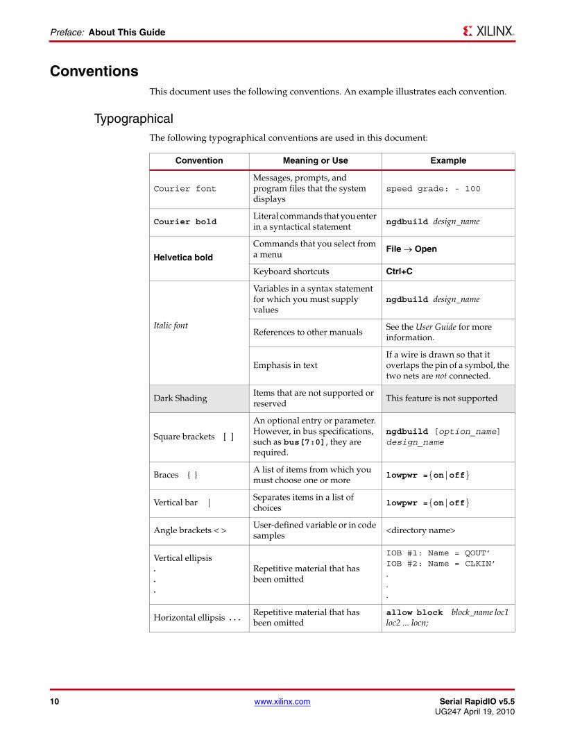
ConventionsThis document uses the following conventions. An example illustrates each convention.
TypographicalThe following typographical conventions are used in this document:
Convention Meaning or Use Example
Courier fontMessages, prompts, and program files that the system displays
speed grade: - 100
Courier boldLiteral commands that you enter in a syntactical statement
ngdbuild design_name
Helvetica bold
Commands that you select from a menu
File → Open
Keyboard shortcuts Ctrl+C
Italic font
Variables in a syntax statement for which you must supply values
ngdbuild design_name
References to other manuals See the User Guide for more information.
Emphasis in textIf a wire is drawn so that it overlaps the pin of a symbol, the two nets are not connected.
Dark ShadingItems that are not supported or reserved
This feature is not supported
Square brackets [ ]
An optional entry or parameter. However, in bus specifications, such as bus[7:0], they are required.
ngdbuild [option_name] design_name
Braces { } A list of items from which you must choose one or more
lowpwr ={on|off}
Vertical bar | Separates items in a list of choices
lowpwr ={on|off}
Angle brackets < > User-defined variable or in code samples
<directory name>
Vertical ellipsis...
Repetitive material that has been omitted
IOB #1: Name = QOUT’ IOB #2: Name = CLKIN’...
Horizontal ellipsis . . .Repetitive material that has been omitted
allow block block_name loc1 loc2 ... locn;
Serial RapidIO v5.5 www.xilinx.com 11UG247 April 19, 2010
Conventions
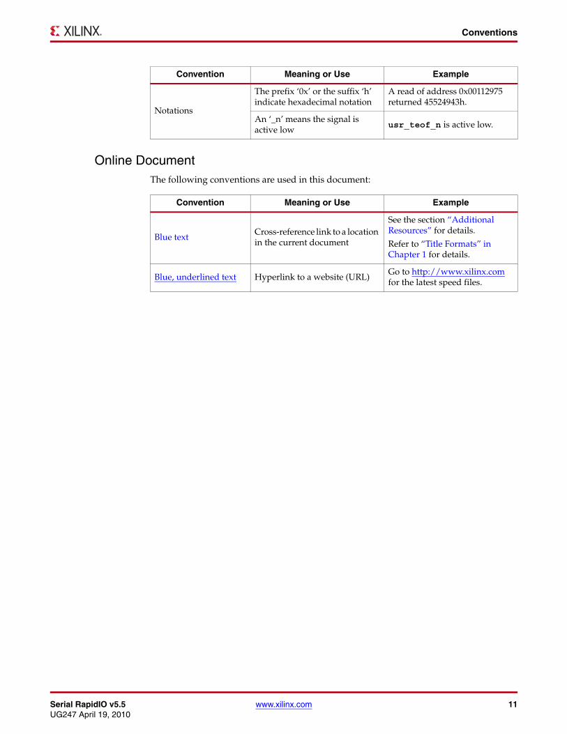
Online DocumentThe following conventions are used in this document:
Notations
The prefix ‘0x’ or the suffix ‘h’ indicate hexadecimal notation
A read of address 0x00112975 returned 45524943h.
An ‘_n’ means the signal is active low usr_teof_n is active low.
Convention Meaning or Use Example
Convention Meaning or Use Example
Blue textCross-reference link to a location in the current document
See the section “Additional Resources” for details.
Refer to “Title Formats” in Chapter 1 for details.
Blue, underlined text Hyperlink to a website (URL)Go to http://www.xilinx.com for the latest speed files.

12 www.xilinx.com Serial RapidIO v5.5UG247 April 19, 2010
Preface: About This Guide
Serial RapidIO v5.5 www.xilinx.com 13UG247 April 19, 2010
Chapter 1
Introduction
The complete LogiCORE™ IP RapidIO Endpoint solution consists of the Serial RapidIO Physical Layer, Buffer, and the RapidIO Logical Layer stitched together with reference designs to create a full example endpoint solution.
• The 1 lane (1x) and 4 lane (4x) Serial Physical Layer is incorporated into the Serial RapidIO Physical Layer core.
• The Logical (I/O) and Transport Layers are combined into the RapidIO Logical Layer core.
The RapidIO Endpoint example design provides the remaining logic to create a RapidIO Endpoint solution that includes a register manager reference design and an example target design. The RapidIO Endpoint example design also provides implementation and simulation scripts for the RapidIO Endpoint solution.
System Requirements
Windows
• Windows XP Professional 32-bit/64-bit
• Windows Vista Business 32-bit/64-bit
Linux
• Red Hat Enterprise Linux WS v4.0 32-bit/64-bit
• Red Hat Enterprise Desktop v5.0 32-bit/64-bit (with Workstation Option)
• SUSE Linux Enterprise (SLE) desktop and server v10.1 32-bit/64-bit
Software
• ISE® software v12.1
Check the release notes for the required service pack; ISE software service packs can be downloaded from www.xilinx.com/xlnx/xil_sw_updates_home.jsp?update=sp.
About the CoreThe Serial RapidIO Endpoint solution, including the Serial RapidIO Physical Layer, Buffer, and the RapidIO Logical Layer cores are Xilinx CORE Generator™ software, included in the latest IP update. For detailed information about these cores, go to www.xilinx.com/rapidio.

14 www.xilinx.com Serial RapidIO v5.5UG247 April 19, 2010
Chapter 1: Introduction
Recommended Design ExperienceThe fully verified RapidIO Endpoint solution allows engineering focus on the unique user-application functions of a RapidIO design. The RapidIO Interconnect technology is a high-performance design that can be challenging to implement in any device technology.
Therefore, previous experience with building high-performance, pipelined FPGA designs using Xilinx implementation software and constraints file is recommended. The challenge to implement a complete RapidIO Endpoint design including user application functions varies, depending on the features and configuration of the application. Contact your local Xilinx representative for a closer review and estimation for your specific requirements.
Additional Core ResourcesFor detailed information about and updates to the RapidIO Design Environment, Serial RapidIO Physical Layer, and the RapidIO Logical Layer coressee the following documents. These and other documents can be downloaded from the Xilinx RapidIO lounge:
www.xilinx.com/rapidio
• Serial RapidIO Release Notes
• Serial RapidIO Data Sheet
• Serial RapidIO User Guide
For updates to this document, see the Serial RapidIO Getting Started Guide, also available from www.xilinx.com/rapidio.
Technical SupportThe fastest method for obtaining specific technical support for the RapidIO cores is through the www.xilinx.com/support website. Questions are routed to a team of engineers with expertise in using the RapidIO cores.
Xilinx will provide technical support for use of this product as described in this guide, the and the LogiCORE IP Serial RapidIO User Guide. Xilinx cannot guarantee timing, functionality, or support of this product for designs that do not follow these guidelines.
FeedbackXilinx welcomes feedback on the RapidIO cores and documentation provided with the cores.
RapidIO CoresFor comments or suggestions about the RapidIO cores, please submit a WebCase at www.xilinx.com/support, and provide the following information:
• Product name
• Core version number
• Brief explanation
Serial RapidIO v5.5 www.xilinx.com 15UG247 April 19, 2010
Feedback
DocumentIf you have any comments about this document, please submit a WebCase at www.xilinx.com/support, and provide the following information:
• Document title
• Document number
• Page number(s) to which your comments refer
• Brief explanation
General suggestions for additions and improvements are also welcome.

16 www.xilinx.com Serial RapidIO v5.5UG247 April 19, 2010
Chapter 1: Introduction
Serial RapidIO v5.5 www.xilinx.com 17UG247 April 19, 2010
Chapter 2
Licensing the Cores
The Serial RapidIO Solution consists of two Xilinx LogiCORE™ IP cores and an endpont reference design. This chapter provides licensing instructions for the Serial RapidIO Physical Layer and the RapidIO Logical Layer cores. You must obtain the appropriate licenses before using the cores in your designs. The Serial RapidIO Physical Layer and RapidIO Logical Layer cores are provided under the terms of the Xilinx LogiCORE Site License Agreement, which conforms to the terms of the SignOnce IP License standard defined by the Common License Consortium. Purchase of a Physical Layer core license includes licensing the Buffer as both are created when generating the Physical Layer.
Purchase of a core entitles you to technical support and access to updates for a period of one year. The endpoint example is a non-licensed support core that includes reference designs, as well as simulation and implementation scripts.
Before you BeginThis chapter assumes you have installed the core using either the CORE Generator™ IP Software Update installer or by performing a manual installation after downloading the core from the web. For information about installing the core, see the RapidIO product page at www.xilinx.com/rapidio.
License Options The Serial RapidIO Physical Layer and RapidIO Logical Layer cores provide three licensing options. After installing the required Xilinx ISE software and IP Service Packs, choose a license option. The endpoint example is a reference design, and is not a licensed core.
Simulation Only The Simulation Only Evaluation license is provided with the Xilinx CORE Generator tool. This license lets you assess core functionality with either the endpoint example design provided in the Serial RapidIO solution, or alongside your own design and demonstrates the various interfaces on the core in simulation. (Functional simulation is supported by a dynamically generated HDL structural model.)
18 www.xilinx.com Serial RapidIO v5.5UG247 April 19, 2010
Chapter 2: Licensing the Cores
Full System Hardware Evaluation The Full System Hardware Evaluation license is available at no cost and lets you fully integrate the core into an FPGA design, place-and-route the design, evaluate timing, and perform functional simulation of the RapidIO endpoint design using the RapidIO endpoint example design and demonstration test bench provided in the Serial RapidIO solution.
In addition, the license key lets you generate a bitstream from the placed and routed design, which can then be downloaded to a supported device and tested in hardware. The core can be tested in the target device for a limited time before timing out (ceasing to function), at which time it can be reactivated by reconfiguring the device.
Full The Full license key is available when you purchase the core and provides full access to all core functionality both in simulation and in hardware, including:
• Functional simulation support • Full implementation support including place and route and bitstream generation • Full functionality in the programmed device with no time outs
Obtaining Your License KeyThis section contains information about obtaining a simulation, full system hardware, and full license keys.
Simulation LicenseNo action is required to obtain the Simulation Only Evaluation license key; it is provided by default with the Xilinx CORE Generator software.
Full System Hardware Evaluation LicenseTo obtain a Full System Hardware Evaluation license, do the following:
1. Navigate to the product page for this core: www.xilinx.com/rapidio
2. Click Download Evaluation. 3. Follow the instructions to install the required Xilinx ISE® software and IP Service
Packs.
Obtaining a Full License KeyTo obtain a Full license key, you must purchase a license for the core. After you purchase a license, a product entitlement is added to your Product Licensing Account on the Xilinx Product Download and Licensing site. The Product Licensing Account Administrator for your site will receive an email from Xilinx with instructions on how to access a Full license and a link to access the licensing site. You can obtain a full key through your account administrator, or your administrator can give you access so that you can generate your own keys.
Further details can be found at http://www.xilinx.com/products/ipcenter/ipaccess_fee.htm.

Serial RapidIO v5.5 www.xilinx.com 19UG247 April 19, 2010
Obtaining Your License Key
Installing Your License FileThe Simulation Only Evaluation license key is provided with the Xilinx ISE software CORE Generator system and does not require installation of an additional license file. For the Full System Hardware Evaluation license and the Full license, an email will be sent to you containing instructions for installing your license file. Additional details about IP license key installation can be found in the ISE Design Suite Installation, Licensing and Release Notes document.

20 www.xilinx.com Serial RapidIO v5.5UG247 April 19, 2010
Chapter 2: Licensing the Cores
Serial RapidIO v5.5 www.xilinx.com 21UG247 April 19, 2010
Chapter 3
Customizing and Generating the Cores
The LogiCORE™ IP Serial RapidIO Design Solution consists of four components, the Serial RapidIO Physical Layer core, Buffer core, the RapidIO Logical Layer core, and the Endpoint example design. These components are generated through the Xilinx CORE Generator™ software using a graphical user interface (GUI).
The 1 lane (1x) and 4 lane (4x) Serial Physical Layer is incorporated into the Serial RapidIO Physical Layer core. The Logical (I/O) and Transport layers are combined into the RapidIO Logical Layer core. The RapidIO Endpoint example design provides the remaining logic to create a Serial RapidIO Endpoint solution that includes a register manager reference design and an example target design.
This chapter describes the GUI options used to generate and customize the cores. When you are generating the Serial RapidIO cores, they must all be created within the same CORE Generator software project directory to work with the Endpoint Example implementation and simulation scripts.
For assistance with starting and using the Xilinx CORE Generator software, see the documentation supplied with the Xilinx ISE® software, including the Xilinx CORE Generator Online Help.
This information is located at toolbox.xilinx.com/docsan/xilinx10/books/manuals.pdf
Serial RapidIO Graphical User InterfaceThis section describes the Xilinx CORE Generator software configurations screens provided to configure the Serial RapidIO Endpoint design.

22 www.xilinx.com Serial RapidIO v5.5UG247 April 19, 2010
Chapter 3: Customizing and Generating the Cores
Main ScreenFigure 3-1 shows the Serial RapidIO CORE Generator software main configuration screen. Descriptions of the GUI options on this screen are provided in the following text.
Component Name
The component name is used as the name of the endpoint reference design as well as the base name of the output files generated for the core. Names must begin with a letter and must be composed from the following characters: a through z, 0 through 9, and "_". The default is srio_v5_5.
Enable Endpoint Example Generation
The Endpoint Example reference design is an option. Enabling this option provides the remaining logic to create a RapidIO Endpoint solution that includes a register manager reference design, an example target design, and implementation and simulation scripts. If the Endpoint Example is not generated, implementation and simulation scripts will not be generated.
X-Ref Target - Figure 3-1
Figure 3-1: Serial RapidIO Configuration Screen

Serial RapidIO v5.5 www.xilinx.com 23UG247 April 19, 2010
Serial RapidIO Graphical User Interface
Enable Serial RapidIO Physical Layer Generation
The Physical Layer core generation is optional. Enabling generation provides a customized netlist for the Physical Layer core, and a netlist for a customized Buffer core. The Physical Layer includes an example transceiver instantiation and associated CORE Generator software files.
Serial RapidIO Physical Layer Name
The Physical Layer name is used as the base name of the output files generated for the Physical Layer core. Names must begin with a letter and be composed from the following characters: a through z, 0 through 9, and "_". The default is srio_phy_v5_5.
Enable Logical and Transport Layer Generation
The Logical Layer core generation is optional. Enabling generation provides a customized netlist for the Logical Layer core and associated CORE Generator software files. The Logical Layer is not meant as a stand-alone core. It is assumed a Physical Layer core will be generated as well.
Logical Layer Name
The Logical Layer name is used as the base name of the output files generated for the logical layer core. Names must begin with a letter and be composed from the following characters: a through z, 0 through 9, and "_". The default is rio_log_io_v5_5.
24 www.xilinx.com Serial RapidIO v5.5UG247 April 19, 2010
Chapter 3: Customizing and Generating the Cores
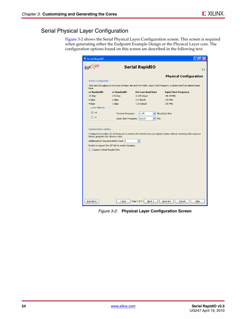
Serial Physical Layer ConfigurationFigure 3-2 shows the Serial Physical Layer Configuration screen. This screen is required when generating either the Endpoint Example Design or the Physical Layer core. The configuration options found on this screen are described in the following text.X-Ref Target - Figure 3-2
Figure 3-2: Physical Layer Configuration Screen
Serial RapidIO v5.5 www.xilinx.com 25UG247 April 19, 2010
Serial RapidIO Graphical User Interface
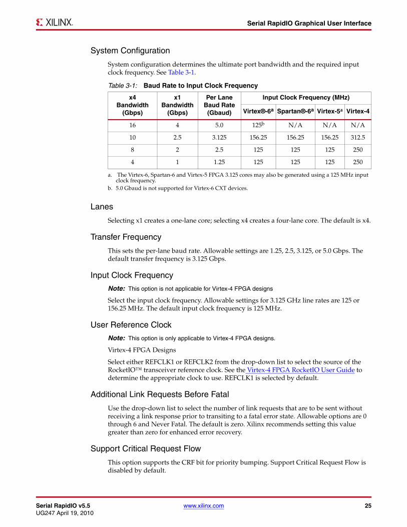
System Configuration
System configuration determines the ultimate port bandwidth and the required input clock frequency. See Table 3-1.
Lanes
Selecting x1 creates a one-lane core; selecting x4 creates a four-lane core. The default is x4.
Transfer Frequency
This sets the per-lane baud rate. Allowable settings are 1.25, 2.5, 3.125, or 5.0 Gbps. The default transfer frequency is 3.125 Gbps.
Input Clock Frequency
Note: This option is not applicable for Virtex-4 FPGA designs
Select the input clock frequency. Allowable settings for 3.125 GHz line rates are 125 or 156.25 MHz. The default input clock frequency is 125 MHz.
User Reference Clock
Note: This option is only applicable to Virtex-4 FPGA designs.
Virtex-4 FPGA Designs
Select either REFCLK1 or REFCLK2 from the drop-down list to select the source of the RocketIO™ transceiver reference clock. See the Virtex-4 FPGA RocketIO User Guide to determine the appropriate clock to use. REFCLK1 is selected by default.
Additional Link Requests Before Fatal
Use the drop-down list to select the number of link requests that are to be sent without receiving a link response prior to transiting to a fatal error state. Allowable options are 0 through 6 and Never Fatal. The default is zero. Xilinx recommends setting this value greater than zero for enhanced error recovery.
Support Critical Request Flow
This option supports the CRF bit for priority bumping. Support Critical Request Flow is disabled by default.
Table 3-1: Baud Rate to Input Clock Frequency
x4 Bandwidth
(Gbps)
x1 Bandwidth
(Gbps)
Per Lane Baud Rate
(Gbaud)
Input Clock Frequency (MHz)
Virtex®-6a
a. The Virtex-6, Spartan-6 and Virtex-5 FPGA 3.125 cores may also be generated using a 125 MHz input clock frequency.
Spartan®-6a Virtex-5a Virtex-4
16 4 5.0 125b
b. 5.0 Gbaud is not supported for Virtex-6 CXT devices.
N/A N/A N/A
10 2.5 3.125 156.25 156.25 156.25 312.5
8 2 2.5 125 125 125 250
4 1 1.25 125 125 125 250
26 www.xilinx.com Serial RapidIO v5.5UG247 April 19, 2010
Chapter 3: Customizing and Generating the Cores
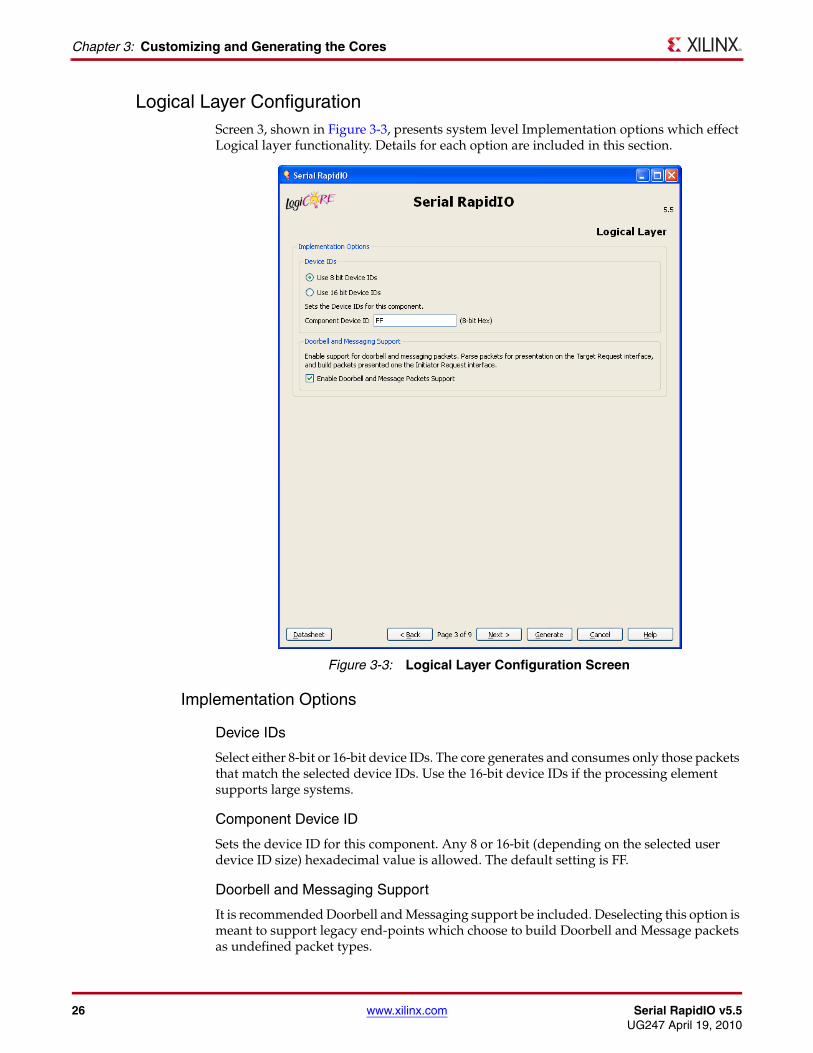
Logical Layer ConfigurationScreen 3, shown in Figure 3-3, presents system level Implementation options which effect Logical layer functionality. Details for each option are included in this section.
Implementation Options
Device IDs
Select either 8-bit or 16-bit device IDs. The core generates and consumes only those packets that match the selected device IDs. Use the 16-bit device IDs if the processing element supports large systems.
Component Device ID
Sets the device ID for this component. Any 8 or 16-bit (depending on the selected user device ID size) hexadecimal value is allowed. The default setting is FF.
Doorbell and Messaging Support
It is recommended Doorbell and Messaging support be included. Deselecting this option is meant to support legacy end-points which choose to build Doorbell and Message packets as undefined packet types.
X-Ref Target - Figure 3-3
Figure 3-3: Logical Layer Configuration Screen

Serial RapidIO v5.5 www.xilinx.com 27UG247 April 19, 2010
Serial RapidIO Graphical User Interface
Buffer Reference Design ConfigurationThe Buffer design options shown in Figure 3-4 provide size vs. bandwidth trade-offs. Descriptions for each option and associated cost are provided in this section. X-Ref Target - Figure 3-4
Figure 3-4: Buffer Design Configuration Screen
28 www.xilinx.com Serial RapidIO v5.5UG247 April 19, 2010
Chapter 3: Customizing and Generating the Cores
Implementation Options
Buffer Configuration
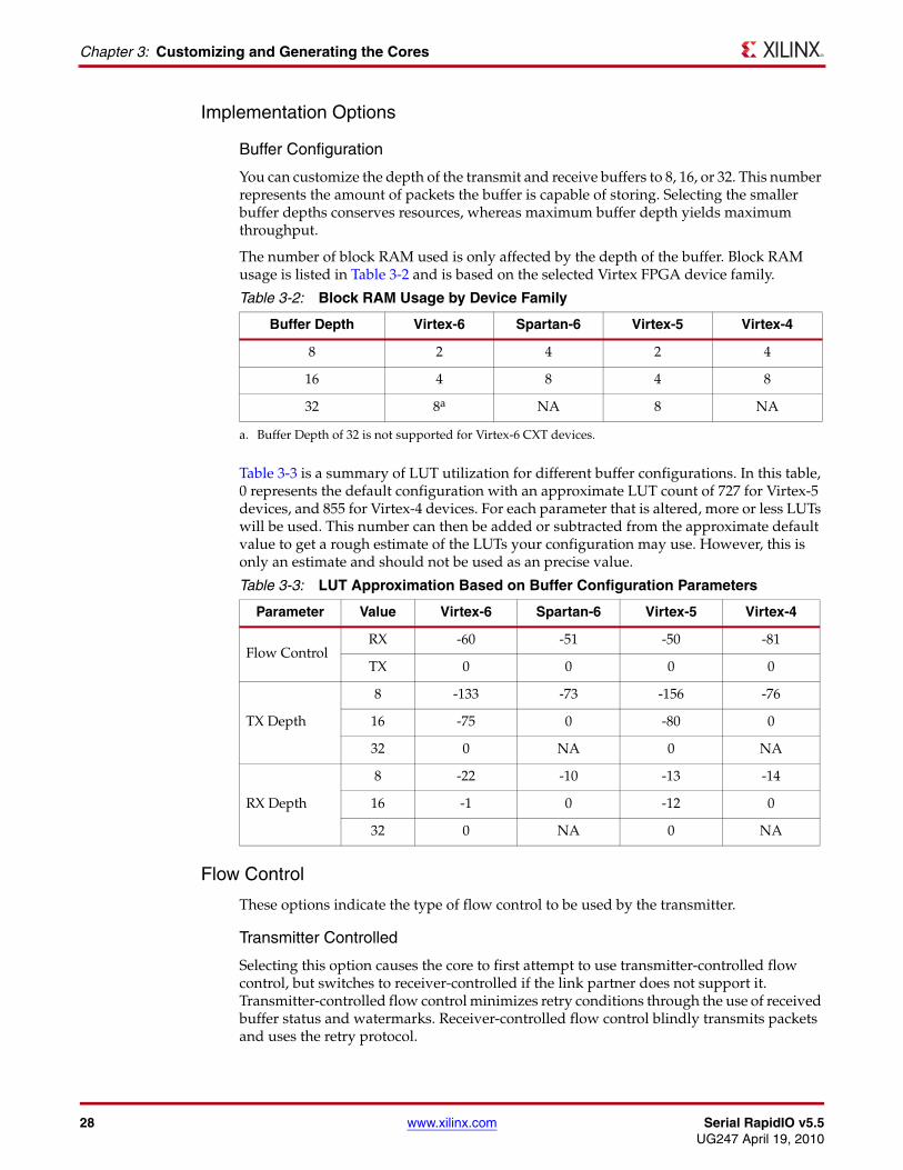
You can customize the depth of the transmit and receive buffers to 8, 16, or 32. This number represents the amount of packets the buffer is capable of storing. Selecting the smaller buffer depths conserves resources, whereas maximum buffer depth yields maximum throughput.
The number of block RAM used is only affected by the depth of the buffer. Block RAM usage is listed in Table 3-2 and is based on the selected Virtex FPGA device family.
Table 3-3 is a summary of LUT utilization for different buffer configurations. In this table, 0 represents the default configuration with an approximate LUT count of 727 for Virtex-5 devices, and 855 for Virtex-4 devices. For each parameter that is altered, more or less LUTs will be used. This number can then be added or subtracted from the approximate default value to get a rough estimate of the LUTs your configuration may use. However, this is only an estimate and should not be used as an precise value.
Flow Control
These options indicate the type of flow control to be used by the transmitter.
Transmitter Controlled
Selecting this option causes the core to first attempt to use transmitter-controlled flow control, but switches to receiver-controlled if the link partner does not support it. Transmitter-controlled flow control minimizes retry conditions through the use of received buffer status and watermarks. Receiver-controlled flow control blindly transmits packets and uses the retry protocol.
Table 3-2: Block RAM Usage by Device Family
Buffer Depth Virtex-6 Spartan-6 Virtex-5 Virtex-4
8 2 4 2 4
16 4 8 4 8
32 8a
a. Buffer Depth of 32 is not supported for Virtex-6 CXT devices.
NA 8 NA
Table 3-3: LUT Approximation Based on Buffer Configuration Parameters
Parameter Value Virtex-6 Spartan-6 Virtex-5 Virtex-4
Flow ControlRX -60 -51 -50 -81
TX 0 0 0 0
TX Depth
8 -133 -73 -156 -76
16 -75 0 -80 0
32 0 NA 0 NA
RX Depth
8 -22 -10 -13 -14
16 -1 0 -12 0
32 0 NA 0 NA

Serial RapidIO v5.5 www.xilinx.com 29UG247 April 19, 2010
Serial RapidIO Graphical User Interface
Receiver Controlled
Select this option for receiver-controlled flow control only. In this mode, packets are blindly transmitted and the retry protocol is used to control packet flow.
Packet Priority Watermarks
Packet Priority Watermarks are used to progressively limit the packet priorities that can be sent as the effective number of free buffers decreases in the link partner. If the free buffer count exceeds the watermark, only packets of that priority and higher are transmitted. Be sure to set the watermark values below the max value of available buffers within the link partner to allow all packet priorities possibility of transmission.
Priority 3 packets will be sent until the effective number of receive buffers reaches zero.
Highest Priority Watermark (WM2)
Used only when in Transmitter Controlled Flow Control Mode. This field establishes the minimum number of available buffer spaces required prior to sending High Priority (priority 2) packets. The watermarks must be constrained to:
0 < WM2 < WM1 < WM0
Medium Priority Watermark (WM1)
Used only when in Transmitter Controlled Flow Control Mode. This field establishes the minimum number of available buffer spaces required prior to sending Medium Priority (priority 1) packets. The watermarks must be constrained to:
0 < WM2 < WM1 < WM0
Smallest Priority Watermark (WM0)
Used only when in Transmitter Controlled Flow Control mode. This field establishes the minimum number of available buffer spaces required prior to sending Smallest Priority (priority 0) packets. The watermarks must be constrained to:
0 < WM2 < WM1 < WM0

30 www.xilinx.com Serial RapidIO v5.5UG247 April 19, 2010
Chapter 3: Customizing and Generating the Cores
Logical Layer CAR ConfigurationThe Logical Layer Device Capabilities Registers (CARs) are detailed in Figure 3-5. These registers are read only once implemented. Register values do not effect core behavior.
Device Capability Registers (CARs)
Device Identity CAR
Device Identity
Xilinx reserved field; currently not used.
Device Vendor Identity
RapidIO Trade Association assigned Xilinx vendor ID.
X-Ref Target - Figure 3-5
Figure 3-5: Logical Layer CAR Configuration (Screen 1)

Serial RapidIO v5.5 www.xilinx.com 31UG247 April 19, 2010
Serial RapidIO Graphical User Interface
Device Information CAR
Device Revision Level
Xilinx core revision.
• Bits 0:15 are currently reserved by Xilinx.
• Bits 16:23 represent the major revision number.
• Bits 24:27 represent the minor revision number.
• Bits 28:31 indicate the patch release.
Currently, the Device Revision Level is 0000_0550h.
Assembly Identity CAR
Assembly Identifier
Sets the type of assembly-CAR 0x08 AssyIdentity field. Any 16-bit hexadecimal value is allowed. The default setting is 0x0000. This does not affect core functionality and is stored in a configuration register.
Assembly Vendor Identifier
Sets the assembly vendor identity-CAR 0x08 AssyVendorIdentity field. Any 16-bit hexadecimal value is allowed. The default setting is 0x0000. This does not affect core functionality and is stored in a configuration register.
Assembly Information CAR
Assembly Revision
Sets the revision for assembly-CAR 0x8 AssyRev field. Any 16-bit hexadecimal value is allowed. The default is 0x0000. This does not affect core functionality and is stored in a configuration register.
Processing Element Features CAR
Selects the major functionality provided by the processing element. Allowable options are:
• Bridge
• Memory
• Processor
Memory is the default setting. This field does not alter core functionality.
32 www.xilinx.com Serial RapidIO v5.5UG247 April 19, 2010
Chapter 3: Customizing and Generating the Cores
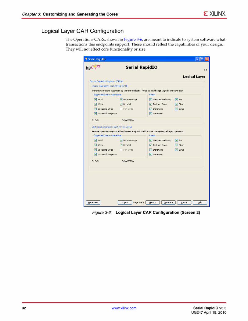
Logical Layer CAR ConfigurationThe Operations CARs, shown in Figure 3-6, are meant to indicate to system software what transactions this endpoints support. These should reflect the capabilities of your design. They will not effect core functionality or size. X-Ref Target - Figure 3-6
Figure 3-6: Logical Layer CAR Configuration (Screen 2)

Serial RapidIO v5.5 www.xilinx.com 33UG247 April 19, 2010
Serial RapidIO Graphical User Interface
Source Operations CAR
Note: Modifications to the Source Operations CAR do not affect core operation. It is an informational register describing the capabilities of the user design.
Supported Source Operations
Select the standard transmit operations supported by the processing element. The supported source operations are listed in the following text. All operations except Port-Write are enabled by default.
• Read
• Write
• Streaming-Write
• Write with Response
• Data Message
• Doorbell
• Port-Write
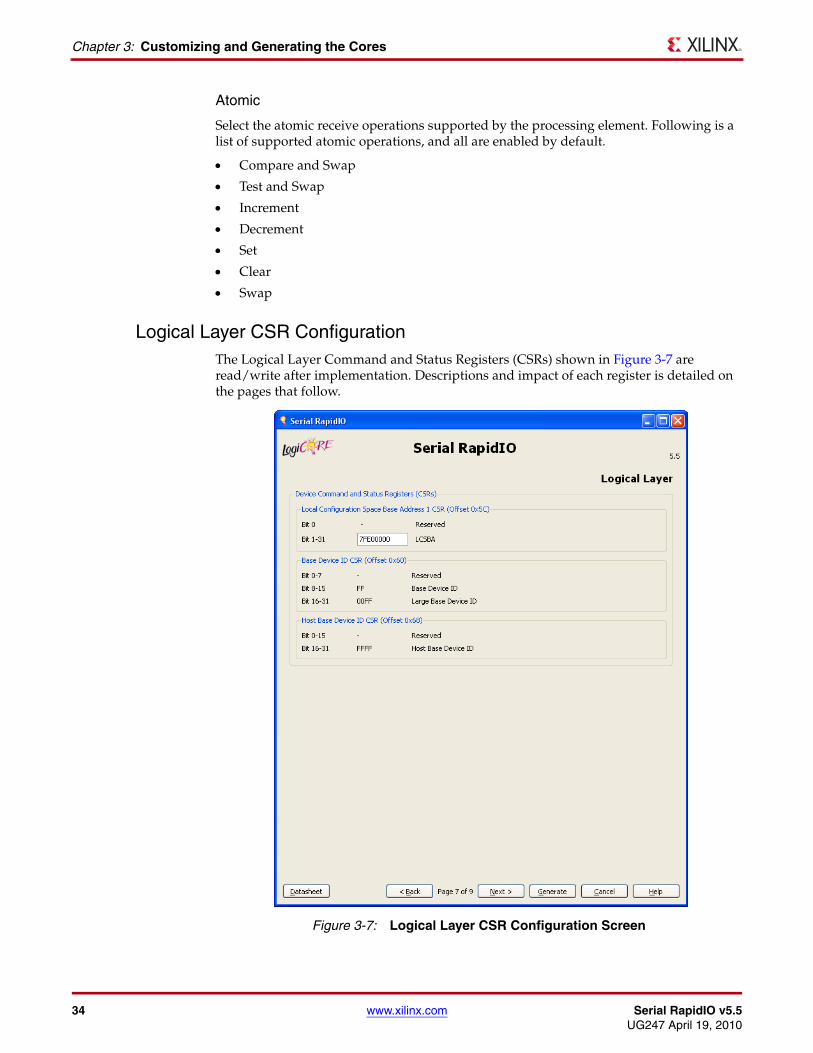
Atomic
Select the atomic transmit operations supported by the processing element. Following is a list of supported atomic operations, and all are enabled by default.
• Compare and Swap
• Test and Swap
• Increment
• Decrement
• Set
• Clear
• Swap
Destination Operations CAR
Note: Modifications to the Destination Operations CAR have no effect on core operation. It is an informational register describing the capabilities of the user design.
Supported Destination Operations
Select the standard receive operations supported by the processing element. Following is a list of supported standard operations. All operations except Port-Write are enable by default.
• Read
• Write
• Streaming-Write
• Write with Response
• Data Message
• Doorbell
• Port-Write
34 www.xilinx.com Serial RapidIO v5.5UG247 April 19, 2010
Chapter 3: Customizing and Generating the Cores
Atomic
Select the atomic receive operations supported by the processing element. Following is a list of supported atomic operations, and all are enabled by default.
• Compare and Swap
• Test and Swap
• Increment
• Decrement
• Set
• Clear
• Swap
Logical Layer CSR ConfigurationThe Logical Layer Command and Status Registers (CSRs) shown in Figure 3-7 are read/write after implementation. Descriptions and impact of each register is detailed on the pages that follow.X-Ref Target - Figure 3-7
Figure 3-7: Logical Layer CSR Configuration Screen
Serial RapidIO v5.5 www.xilinx.com 35UG247 April 19, 2010
Serial RapidIO Graphical User Interface
Device Command and Status Registers (CSRs)
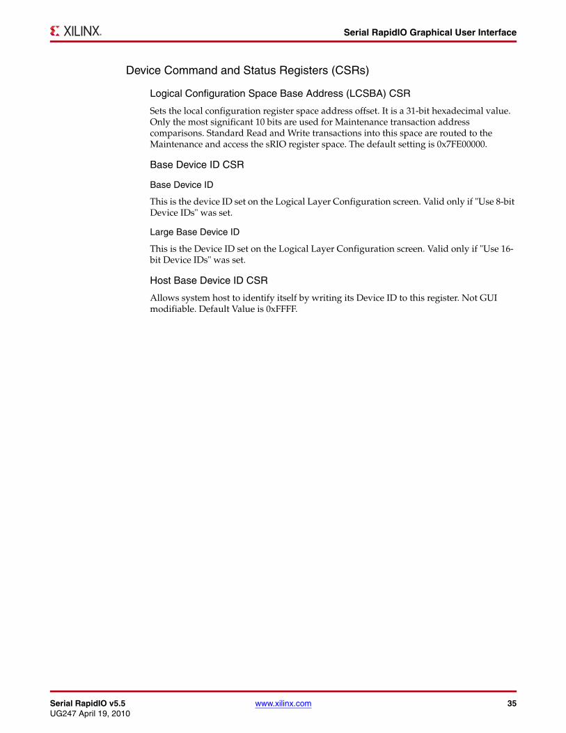
Logical Configuration Space Base Address (LCSBA) CSR
Sets the local configuration register space address offset. It is a 31-bit hexadecimal value. Only the most significant 10 bits are used for Maintenance transaction address comparisons. Standard Read and Write transactions into this space are routed to the Maintenance and access the sRIO register space. The default setting is 0x7FE00000.
Base Device ID CSR
Base Device ID
This is the device ID set on the Logical Layer Configuration screen. Valid only if "Use 8-bit Device IDs" was set.
Large Base Device ID
This is the Device ID set on the Logical Layer Configuration screen. Valid only if "Use 16-bit Device IDs" was set.
Host Base Device ID CSR
Allows system host to identify itself by writing its Device ID to this register. Not GUI modifiable. Default Value is 0xFFFF.
36 www.xilinx.com Serial RapidIO v5.5UG247 April 19, 2010
Chapter 3: Customizing and Generating the Cores
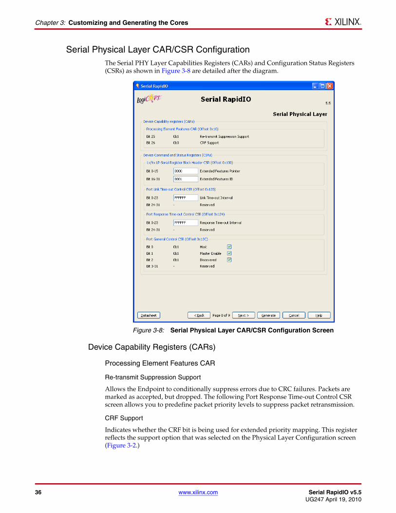
Serial Physical Layer CAR/CSR ConfigurationThe Serial PHY Layer Capabilities Registers (CARs) and Configuration Status Registers (CSRs) as shown in Figure 3-8 are detailed after the diagram.
Device Capability Registers (CARs)
Processing Element Features CAR
Re-transmit Suppression Support
Allows the Endpoint to conditionally suppress errors due to CRC failures. Packets are marked as accepted, but dropped. The following Port Response Time-out Control CSR screen allows you to predefine packet priority levels to suppress packet retransmission.
CRF Support
Indicates whether the CRF bit is being used for extended priority mapping. This register reflects the support option that was selected on the Physical Layer Configuration screen (Figure 3-2.)
X-Ref Target - Figure 3-8
Figure 3-8: Serial Physical Layer CAR/CSR Configuration Screen

Serial RapidIO v5.5 www.xilinx.com 37UG247 April 19, 2010
Serial RapidIO Graphical User Interface
Device Command and Status Registers (CSRs)
1x/4x LP-Serial Register Block Header CSR
Sets the extended features ID. The extended features ID indicates the extended features of the core. The allowable range is any 16-bit hexadecimal value 0000h to FFFFh. The default is 0001h to reflect the endpoint functionality of the core.
Port Link Time-out Control CSR
Time-out value the PHY uses when determining a link control symbol, such as Packet Accepted or Link Response, has been lost. When this counter expires, link protocol as defined in the RapidIO Serial PHY specification is followed. The max time-out scales linearly with the value in this CSR. A max time-out value of FF_FFFFh corresponds to a time-out length of approximately 3.33 seconds.
Port Response Time-out Control CSR
Time-out value to be used by an end-point to determine a lost packet. A max time-out value of FF_FFFFh should correspond to a time-out length of approximately 3.33 seconds.
Port General Control CSR
The Host bit indicates that the device is a host device. If this bit is not set, the device is an agent or a slave. This bit does not affect core functionality.
The Master Enable bit controls whether or not a device is allowed to issue requests to the system. If the Master Enable bit is not set, the device may only respond to requests.
The Discovered bit indicates that the device has been located by the processing element responsible for system configuration. This bit does not affect endpoint operation.

38 www.xilinx.com Serial RapidIO v5.5UG247 April 19, 2010
Chapter 3: Customizing and Generating the Cores
Serial Physical Layer CSR ConfigurationThe port control CSR is Configurable using the Serial Physical Layer CSR Configuration screen (Figure 3-9). Details on each field are provided in this section.
CSR Port MAP
Sets the port (defined in the RapidIO CSR map) to which CSR transactions are targeted. The allowable range is any single hexadecimal value of 0 through F. The default is zero (0). A change to this value modifies the PHY port CSR address offsets.
Command and Status Register
Port Width Override
This sets the default port width for 4x configurations. Default is No Override.
• No Override keeps the 4x configuration in 4x mode.
• Force Single Lane 0 causes the 4x configuration to operate in 1x mode on Lane 0.
• Force Single Lane 2 causes the 4x configuration to operate in 1x mode on Lane 2.
X-Ref Target - Figure 3-9
Figure 3-9: Serial Physical Layer CSR Configuration Screen
Serial RapidIO v5.5 www.xilinx.com 39UG247 April 19, 2010
Serial RapidIO Graphical User Interface
Port Disable
Enabling this option disables port receivers and drivers (serial transceivers). When disabled, the port is unable to transmit or receive packets and control symbols. The port is enabled (unchecked) by default.
Output Port Enable
This enables transmission on the output port. When disabled, the port can only transmit maintenance packets; control packets are unaffected. Output Port Enable is enabled by default.
Input Port Enable
This enables reception on the input port. When disabled, the port can only receive maintenance packets. Non-maintenance packets generate packet-not-accepted (PNA) control symbols. Control symbols are unaffected. Input Port Enable is enabled by default.
Error Checking Disable
Select this option to disable all error checking. Doing so causes all packets to be passed to the link interface, and all packets are tagged as accepted. Core behavior is undefined when this option is selected and a packet with an error is received. Error Checking is enabled (unchecked) by default.
Multicast Event Participant
Select this option to set the core as a multicast event participant. This causes multicast event control symbols to be sent to this port. Multicast Event Participation is enabled by default.
Re-transmit Suppression Mask
Conditionally suppress CRC errors based on packet priority. Extended priority through CRF is available only if CRF support is enabled on the Serial Physical Layer CSR Configuration screen (Figure 3-8.)

40 www.xilinx.com Serial RapidIO v5.5UG247 April 19, 2010
Chapter 3: Customizing and Generating the Cores
Output GenerationThe output files generated from the Xilinx CORE Generator™ software are placed in the project directory. The file output list may include some or all of the following files. For complete descriptions of these output files, see “Directory Structure and File Descriptions” in Chapter 5.
• Serial RapidIO Physical Layer netlist
• RapidIO Logical Layer netlist
• Serial RapidIO Buffer netlist
• Serial RapidIO Physical Layer simulation model
• RapidIO Logical Layer simulation model
• Supporting CORE Generator software files
• Serial RapidIO release notes and other documentation
• Register Manager reference design
• Serial RapidIO endpoint example design
• Synthesis and implementation scripts
• Mentor Graphics® ModelSim®, Cadence® Incisive Enterprise Simulator (IES), and and Synopsys® VCS® functional simulation scripts
• Clocking template and user constraint file

Serial RapidIO v5.5 www.xilinx.com 41UG247 April 19, 2010
Chapter 4
Quick Start Example Design
This chapter introduces the RapidIO Endpoint reference design that is included with the Serial RapidIO Endpoint solution. The reference design demonstrates how to generate the Serial RapidIO Endpoint solution, including the Serial RapidIO Physical Layer, Buffer design and RapidIO Logical Layer cores, and illustrates using the default options in the RapidIO Endpoint example design. For detailed information about the example design, see Chapter 5, “Detailed Example Design.”
OverviewFigure 4-1 shows the Serial RapidIO Endpoint example design, which contains a simulation host model interfacing to a target design that writes and reads data to memory. Both the simulation host and the user design use the RapidIO Endpoint reference design, consisting of a Serial RapidIO Physical Layer core, Buffer core, RapidIO Logical Layer core, and Register Manager reference design. For a description of the components provided with the Serial RapidIO Endpoint, see “Chapter 5, “Detailed Example Design.”
For detailed information about the Serial RapidIO Physical Layer and the RapidIO Logical Layer cores, see the Serial RapidIO User Guide.

42 www.xilinx.com Serial RapidIO v5.5UG247 April 19, 2010
Chapter 4: Quick Start Example Design
Generating the CoresBefore you can use the Serial RapidIO Endpoint solution, the Serial RapidIO Physical Layer and RapidIO Logical Layer cores must be generated in the CORE Generator™ software within the same CORE Generator software project directory. To generate these cores, you must first create a CORE Generator software project.
To create a CORE Generator software project:
1. Start the CORE Generator software.
For help starting the CORE Generator software, see the Xilinx CORE Generator Guide.
2. Choose File > New Project.
3. Type a directory name. In this example, the directory is named <project_dir>.
X-Ref Target - Figure 4-1
Figure 4-1: The RapidIO Endpoint Example Design Configuration
SerialPhysical
Layer
SerialPhysical
Layer
UserDesign
SimulationHost
Logical (IO)and
TransportLayer
Logical (IO)and
TransportLayer
BufferDesign
BufferDesign
Register Manager Register Manager
ep_tb.vep_sim.v<rio_de_component_name>_top.v
InitiatorUser
Design
TargetUser
Design
InitiatorSimulation
Design
TargetUser
Design

Serial RapidIO v5.5 www.xilinx.com 43UG247 April 19, 2010
Generating the Cores
4. Set the following options:
Part Options:
a. From Target Architecture, select the desired Virtex® device family. Supported families include Virtex-6, Spartan-6 LXT, Virtex-5 LXT/FXT, and Virtex-4 FX devices.
Note: If an unsupported silicon family is selected, the RapidIO cores will not appear in the list of available cores.
Note: The Device, Package, and Speed Grade selected in the Part options tab have no effect on the generated cores. The core is delivered with an example UCF, targeting the Virtex-6 XC6VLX240T-1156-1, Spartan-6 XC6SLX45T-FGG484-2, Virtex-5 XC5VLX50T-FF1136-1, Virtex-5 XC5VFX70TFF1136-1, or Virtex-4 XC4VFX60-FF1152-10, depending on the chosen target architecture.
Generation Options:
b. Select either VHDL or Verilog for the Design Entry.
Note: A VHDL reference design is not supported for Virtex-4 devices.
c. For Vendor, select Synplicity or Other (for XST).
Advanced Options:
Leave the advanced options at their default values.
To generate a Full Serial RapidIO Endpoint with default values
1. After creating the project, locate the directory containing Serial RapidIO in the list of available cores. It should be located under Standard Bus Interfaces > RapidIO > Serial RapidIO.
2. Double-click the Serial RapidIO core.
If the license file is not properly configured, the CORE Generator software displays an error. See Chapter 2, “Licensing the Cores” for details.
3. If a warning appears regarding the limitations of the available license, click OK.
The Serial RapidIO customization screen appears.
4. Accept the default values on the screen, and then click Finish.
By default, the cores are named srio_phy_v5_5 and rio_log_io_v5_5 and are generated into the Component Name directory within the project directory. Also generated in the Component Name directory are the supporting files for the core, including the Serial RapidIO example endpoint design. Detailed information about the files and directories delivered with the Serial RapidIO core is provided in the following chapter, “Directory Structure and File Descriptions,” page 47.
44 www.xilinx.com Serial RapidIO v5.5UG247 April 19, 2010
Chapter 4: Quick Start Example Design
Implementing the Example DesignAfter the Serial RapidIO cores are generated, the Serial RapidIO Endpoint example design can be synthesized by XST or Synplify, depending on the Vendor setting chosen in the CORE Generator software project options, and processed by the Xilinx implementation tools. The output files generated by the Serial RapidIO Endpoint solution include scripts to assist you in running synthesis and implementation.
In the implementation example that follows, srio_v5_5 is the component name as generated by default from the Serial RapidIO Endpoint solution configuration screen. If a core is generated with a different name, substitute that core name in the following commands.
• From the CORE Generator software project directory window, type the following to implement the Serial RapidIO Endpoint example design.
Windows
> cd srio_v5_5\implement> implement.bat
Linux
% cd srio_v5_5/implement% ./implement.sh
These commands execute a script that synthesizes, builds, maps, and place-and-routes the Serial RapidIO Endpoint example design including the Serial RapidIO Physical Layer and RapidIO Logical Layer core netlists. The resulting files are placed in the results directory of the Serial RapidIO Endpoint solution, which is created by the implement script at runtime.
Running the Simulation Using the Serial RapidIO Endpoint example design (delivered as part of the Serial RapidIO Endpoint solution), you can quickly simulate and observe the behavior of the RapidIO cores.
Setting up the SimulationTo run the gate-level simulation you must have the Xilinx Simulation Libraries compiled for your system. See the Compiling Xilinx Simulation Libraries (COMPXLIB) in the Xilinx ISE® Synthesis and Verification Design Guide, and the Xilinx ISE Software Manuals and Help. You can download these documents from: www.xilinx.com/support/software_manuals.htm.
The Xilinx simulation libraries must be mapped into the simulator. If the libraries are not set for your environment, please refer to the Synthesis and Simulation Design Guide on the Xilinx software manuals Web page for assistance compiling Xilinx simulation models and setting up the simulator environment.
Virtex-6, Spartan-6, and Virtex-5 devices require a Verilog LRM-IEEE 1364-2005 encryption-compliant simulator. For VHDL simulation, a mixed HDL license is required.

Serial RapidIO v5.5 www.xilinx.com 45UG247 April 19, 2010
Creating an ISE Software Project
Functional Simulation This section contains instructions for running a functional simulation of the Serial RapidIO Endpoint solution using Verilog. Functional simulation models for the Serial RapidIO Physical Layer and RapidIO Logical Layer cores are provided when the cores are generated. Implementing the core before simulating the functional models is not required.
In the following simulation examples, the defaults of <project_dir> for the CORE Generator software project directory, and srio_v5_5 for the component name of the Serial RapidIO Endpoint solution are used. If you generate the core with a different name, substitute that component name in the following commands.
To run the functional simulation of the example design using ModelSim:
1. Launch the ModelSim simulator and set the current directory to
<project_dir>/srio_v5_5/simulation/functional
2. Launch the simulation script:
modelsim> do simulate_mti.do
To run the functional simulation of the example design using IES:
1. Set the current directory to:
<project_dir>/srio_v5_5/simulation/functional
2. Execute the simulation script:
% ./simulate_ncsim.sh> ./simulate_ncsim.bat
The simulation script compiles the Serial RapidIO Physical Layer, Buffer, RapidIO Logical Layer functional simulation models, the Serial RapidIO Endpoint example design, and supporting simulation files. It then runs the simulation and checks ensure that it completed successfully. To observe the operation of the core, inspect the simulation transcript and the waveform.
Creating an ISE Software ProjectLocated in the top level of your project directory is a create_ise_prj.tcl script. This script allows for easily integrating the Serial RapidIO core into an ISE software project using Project Navigator. The script creates a new project and locates all the necessary files and directories to synthesize the SRIO core. This script only supports a core generated outside of Project Navigator using the CORE Generator software with all components of the full solution selected (that is, Endpoint Example Design, Serial RapidIO Logical Layer, and Serial RapidIO Physical Layer).
To use this script, from a command prompt navigate into your project directory where this script is located. Run the command “xtclsh create_ise_prj.tcl build_project”. After this script executes, a .ise file will be located in the same directory. It can then be opened to work with the project or implement the core through XST.

46 www.xilinx.com Serial RapidIO v5.5UG247 April 19, 2010
Chapter 4: Quick Start Example Design
Serial RapidIO v5.5 www.xilinx.com 47UG247 April 19, 2010
Chapter 5
Detailed Example Design
This chapter provides detailed information about the Serial RapidIO Endpoint example design. It describes the output files, directory structure, purpose and contents of the implementation scripts, operation of the example target design and the demonstration test bench.
Directory Structure and File DescriptionsThe complete LogiCORE™ IP Serial RapidIO Endpoint solution consists of the following cores:
• Serial RapidIO Physical Layer
• Buffer Design
• RapidIO Logical Layer
• Serial RapidIO Endpoint Example Design
The 1 lane (1x) and 4 lane (4x) Serial Physical Layer is incorporated into the Serial RapidIO Physical Layer core. The Logical (I/O) and Transport layers are combined into the RapidIO Logical Layer core. The RapidIO Endpoint solution includes a register manager reference design, and an example user design.
The Serial RapidIO Endpoint solution also includes synthesis and implementation scripts, simulation scripts, a demonstration test bench, and supporting simulation files for the example design. For the implementation and simulation scripts to work, all cores must be generated in the same CORE Generator™ software project directory.
As illustrated in the following directory structure, the CORE Generator software project is <project_dir>; the component name for the Serial RapidIO Physical Layer core is <phy_component_name>; the component name for the RapidIO Logical Layer core is <logio_component_name>; and the component name for the Serial RapidIO Endpoint solution is <srio_component_name>.
48 www.xilinx.com Serial RapidIO v5.5UG247 April 19, 2010
Chapter 5: Detailed Example Design
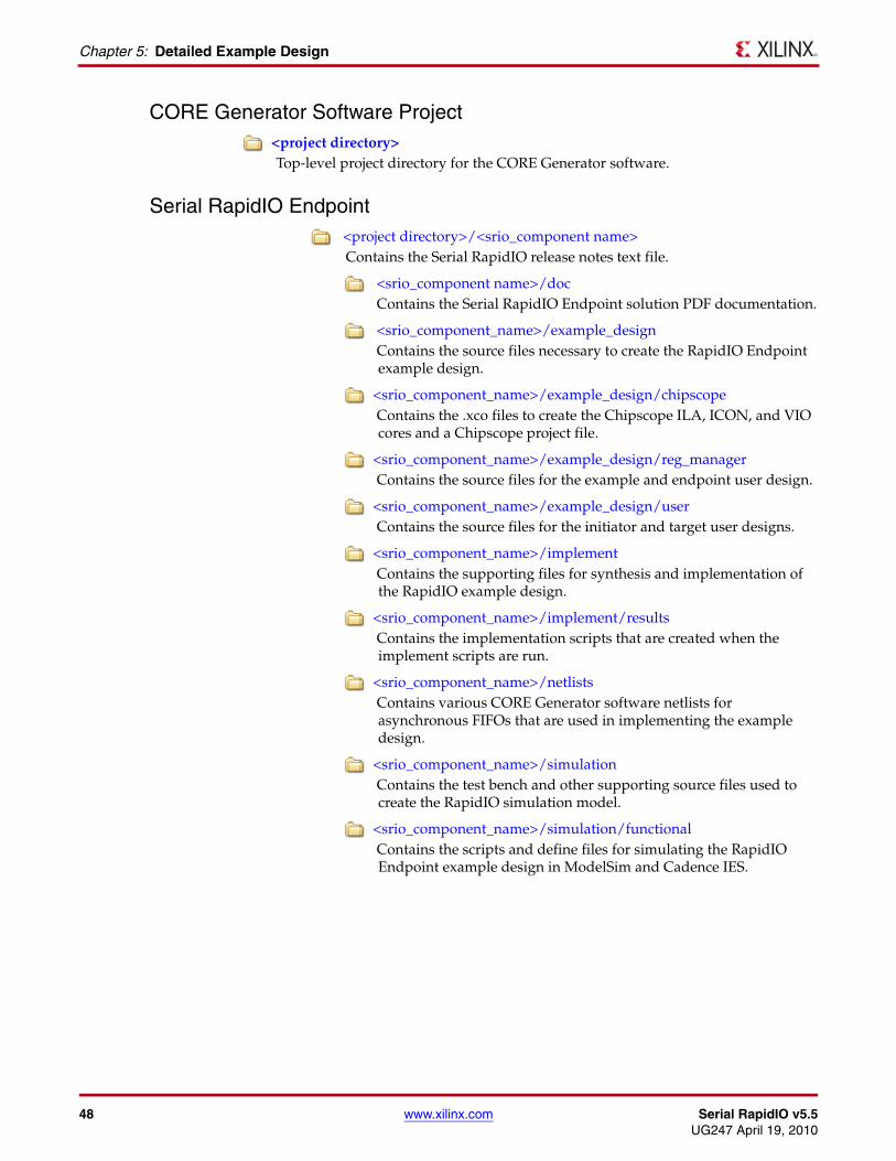
CORE Generator Software Project<project directory>Top-level project directory for the CORE Generator software.
Serial RapidIO Endpoint <project directory>/<srio_component name>Contains the Serial RapidIO release notes text file.
<srio_component name>/docContains the Serial RapidIO Endpoint solution PDF documentation.
<srio_component_name>/example_designContains the source files necessary to create the RapidIO Endpoint example design.
<srio_component_name>/example_design/chipscopeContains the .xco files to create the Chipscope ILA, ICON, and VIO cores and a Chipscope project file.
<srio_component_name>/example_design/reg_managerContains the source files for the example and endpoint user design.
<srio_component_name>/example_design/userContains the source files for the initiator and target user designs.
<srio_component_name>/implementContains the supporting files for synthesis and implementation of the RapidIO example design.
<srio_component_name>/implement/resultsContains the implementation scripts that are created when the implement scripts are run.
<srio_component_name>/netlistsContains various CORE Generator software netlists for asynchronous FIFOs that are used in implementing the example design.
<srio_component_name>/simulationContains the test bench and other supporting source files used to create the RapidIO simulation model.
<srio_component_name>/simulation/functionalContains the scripts and define files for simulating the RapidIO Endpoint example design in ModelSim and Cadence IES.
Serial RapidIO v5.5 www.xilinx.com 49UG247 April 19, 2010
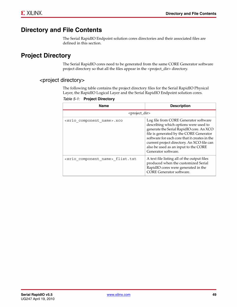
Directory and File Contents
Directory and File ContentsThe Serial RapidIO Endpoint solution cores directories and their associated files are defined in this section.
Project DirectoryThe Serial RapidIO cores need to be generated from the same CORE Generator software project directory so that all the files appear in the <project_dir> directory.
<project directory>The following table contains the project directory files for the Serial RapidIO Physical Layer, the RapidIO Logical Layer and the Serial RapidIO Endpoint solution cores.
Table 5-1: Project Directory
Name Description
<project_dir>
<srio_component_name>.xco Log file from CORE Generator software describing which options were used to generate the Serial RapidIO core. An XCO file is generated by the CORE Generator software for each core that it creates in the current project directory. An XCO file can also be used as an input to the CORE Generator software.
<srio_component_name>_flist.txt A text file listing all of the output files produced when the customized Serial RapidIO cores were generated in the CORE Generator software.

50 www.xilinx.com Serial RapidIO v5.5UG247 April 19, 2010
Chapter 5: Detailed Example Design
Serial RapidIO Endpoint SolutionThe following tables contain the files and their descriptions specific to the Serial RapidIO Endpoint solution.
<project directory>/<srio_component name>The <srio_component_name> directory contains the release notes text file included with the core that contains last-minute changes and or updates.
Table 5-2: Component Name Directory
Name Description
<project_dir>/<srio_component_name>
srio_readme.txt The Serial RapidIO Endpoint core release notes text file.
create_ise_prj.tcl A TCL script to simplify creating an ISE® software project.
<phy_component_name>.ngc The netlist for the Serial RapidIO Physical Layer core.
<phy_component_name>.ngc The netlist for the RapidIO Physical Layer core.
<phy_component_name>.v
<phy_component_name>.vhd
The structural simulation model for the Serial RapidIO Physical Layer core. It is used to support the functional simulation of the Serial RapidIO Physical Layer core in the RapidIO Endpoint example design.
<phy_component_name>.veo
<phy_component_name>.vho
The HDL template for the Serial RapidIO Physical Layer.
<logio_component_name>.ngc The netlist for the RapidIO Logical Layer core.
<logio_component_name>.v
<logio_component_name>.vhd
The structural simulation model for the RapidIO Logical Layer core. It is used to support the functional simulation of the Serial RapidIO Physical Layer core in the RapidIO Endpoint example design.
<logio_component_name>.veo
<logio_component_name>.vho
The HDL template for the RapidIO Logical Layer core.
rio_buffer.ngc The netlist for the Buffer design.
rio_buffer.v
rio_buffer.vhd
The structural simulation model for the Buffer design. It is used to support the functional simulation of the Buffer in the RapidIO Endpoint example design.
rio_buffer.veo
rio_buffer.vho
The HDL template for the Buffer.
“<project directory>”

Serial RapidIO v5.5 www.xilinx.com 51UG247 April 19, 2010
Serial RapidIO Endpoint Solution
<srio_component name>/docThis directory contains the Serial RapidIO Endpoint solution PDF documentation that is included with the core.
<srio_component_name>/example_designThis directory and its subdirectories contain all the source files, aside from the Serial RapidIO Physical Layer and RapidIO Logical Layer netlists, to create the RapidIO Endpoint example design. They include the Buffer design, register manager reference design, example user design, and user constraints file.
Table 5-3: Doc Directory
Name Description
<project_dir>/<srio_component_name>/doc
srio_gsg247.pdf The Serial RapidIO Getting Started Guide
srio_ds696.pdf The Serial RapidIO Data Sheet
srio_ug503.pdf The Serial RapidIO User Guide
“<project directory>”
Table 5-4: Example Design Directory
Name Description
<project_dir>/<srio_component_name>/example_design
<srio_component_name>_top.ucf The user constraints file (UCF) for the RapidIO Endpoint example design.
<srio_component_name>_top.v
<srio_component_name>_top.vhd
The top-level HDL file for the RapidIO Endpoint example design.
<srio_component_name>_clk.v
<srio_component_name>_clk.vhd
HDL clock module for generation of reference clocks and core clocks.
rio_wrapper.v
rio_wrapper.vhd
HDL wrapper file that instantiates the SRIO Physical Layer core, RapidIO Logical Layer core, Buffer design, Register Manager reference design, and transceiver wrapper. The SRIO Physical Layer core and Serial RapidIO GT wrapper are instantiated as part of the Physical Layer wrapper.
phy_wrapper.vphy_wrapper.vhd
Wrapper file that instantiates SRIO Physical Layer core and the SRIO GT transceiver wrapper.
rio_reset.vrio_reset.vhd
Example reset module that generates and sequences the necessary resets from a sys_reset_n.
srio_gt_wrapper_v4_1x.v Transceiver wrapper file for Virtex®-4 FPGA 1x configurations.
srio_gt_wrapper_v4_4x.v Transceiver wrapper file for Virtex-4 FPGA 4x configurations.
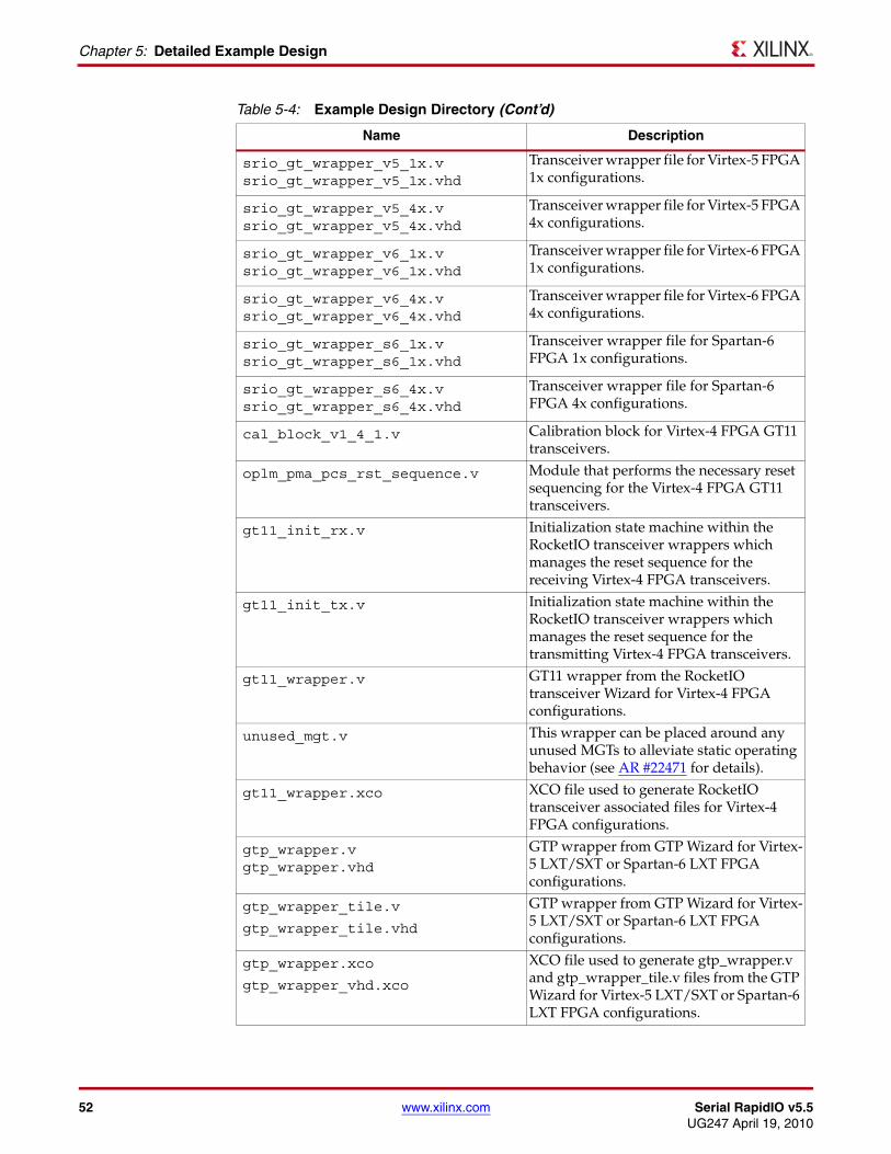
52 www.xilinx.com Serial RapidIO v5.5UG247 April 19, 2010
Chapter 5: Detailed Example Design
srio_gt_wrapper_v5_1x.vsrio_gt_wrapper_v5_1x.vhd
Transceiver wrapper file for Virtex-5 FPGA 1x configurations.
srio_gt_wrapper_v5_4x.vsrio_gt_wrapper_v5_4x.vhd
Transceiver wrapper file for Virtex-5 FPGA 4x configurations.
srio_gt_wrapper_v6_1x.vsrio_gt_wrapper_v6_1x.vhd
Transceiver wrapper file for Virtex-6 FPGA 1x configurations.
srio_gt_wrapper_v6_4x.vsrio_gt_wrapper_v6_4x.vhd
Transceiver wrapper file for Virtex-6 FPGA 4x configurations.
srio_gt_wrapper_s6_1x.vsrio_gt_wrapper_s6_1x.vhd
Transceiver wrapper file for Spartan-6 FPGA 1x configurations.
srio_gt_wrapper_s6_4x.vsrio_gt_wrapper_s6_4x.vhd
Transceiver wrapper file for Spartan-6 FPGA 4x configurations.
cal_block_v1_4_1.v Calibration block for Virtex-4 FPGA GT11 transceivers.
oplm_pma_pcs_rst_sequence.v Module that performs the necessary reset sequencing for the Virtex-4 FPGA GT11 transceivers.
gt11_init_rx.v Initialization state machine within the RocketIO transceiver wrappers which manages the reset sequence for the receiving Virtex-4 FPGA transceivers.
gt11_init_tx.v Initialization state machine within the RocketIO transceiver wrappers which manages the reset sequence for the transmitting Virtex-4 FPGA transceivers.
gt11_wrapper.v GT11 wrapper from the RocketIO transceiver Wizard for Virtex-4 FPGA configurations.
unused_mgt.v This wrapper can be placed around any unused MGTs to alleviate static operating behavior (see AR #22471 for details).
gt11_wrapper.xco XCO file used to generate RocketIO transceiver associated files for Virtex-4 FPGA configurations.
gtp_wrapper.vgtp_wrapper.vhd
GTP wrapper from GTP Wizard for Virtex-5 LXT/SXT or Spartan-6 LXT FPGA configurations.
gtp_wrapper_tile.v
gtp_wrapper_tile.vhd
GTP wrapper from GTP Wizard for Virtex-5 LXT/SXT or Spartan-6 LXT FPGA configurations.
gtp_wrapper.xco
gtp_wrapper_vhd.xco
XCO file used to generate gtp_wrapper.v and gtp_wrapper_tile.v files from the GTP Wizard for Virtex-5 LXT/SXT or Spartan-6 LXT FPGA configurations.
Table 5-4: Example Design Directory (Cont’d)
Name Description
Serial RapidIO v5.5 www.xilinx.com 53UG247 April 19, 2010
Serial RapidIO Endpoint Solution
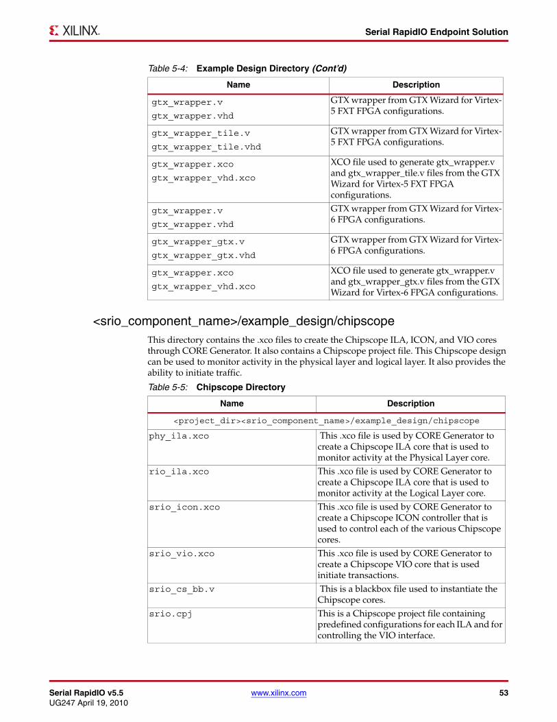
<srio_component_name>/example_design/chipscopeThis directory contains the .xco files to create the Chipscope ILA, ICON, and VIO cores through CORE Generator. It also contains a Chipscope project file. This Chipscope design can be used to monitor activity in the physical layer and logical layer. It also provides the ability to initiate traffic.
gtx_wrapper.v
gtx_wrapper.vhd
GTX wrapper from GTX Wizard for Virtex-5 FXT FPGA configurations.
gtx_wrapper_tile.v
gtx_wrapper_tile.vhd
GTX wrapper from GTX Wizard for Virtex-5 FXT FPGA configurations.
gtx_wrapper.xco
gtx_wrapper_vhd.xco
XCO file used to generate gtx_wrapper.v and gtx_wrapper_tile.v files from the GTX Wizard for Virtex-5 FXT FPGA configurations.
gtx_wrapper.v
gtx_wrapper.vhd
GTX wrapper from GTX Wizard for Virtex-6 FPGA configurations.
gtx_wrapper_gtx.v
gtx_wrapper_gtx.vhd
GTX wrapper from GTX Wizard for Virtex-6 FPGA configurations.
gtx_wrapper.xco
gtx_wrapper_vhd.xco
XCO file used to generate gtx_wrapper.v and gtx_wrapper_gtx.v files from the GTX Wizard for Virtex-6 FPGA configurations.
Table 5-4: Example Design Directory (Cont’d)
Name Description
Table 5-5: Chipscope Directory
Name Description
<project_dir><srio_component_name>/example_design/chipscope
phy_ila.xco This .xco file is used by CORE Generator to create a Chipscope ILA core that is used to monitor activity at the Physical Layer core.
rio_ila.xco This .xco file is used by CORE Generator to create a Chipscope ILA core that is used to monitor activity at the Logical Layer core.
srio_icon.xco This .xco file is used by CORE Generator to create a Chipscope ICON controller that is used to control each of the various Chipscope cores.
srio_vio.xco This .xco file is used by CORE Generator to create a Chipscope VIO core that is used initiate transactions.
srio_cs_bb.v This is a blackbox file used to instantiate the Chipscope cores.
srio.cpj This is a Chipscope project file containing predefined configurations for each ILA and for controlling the VIO interface.
54 www.xilinx.com Serial RapidIO v5.5UG247 April 19, 2010
Chapter 5: Detailed Example Design
<srio_component_name>/example_design/reg_managerThis directory contains the source files for the Register Manager reference design. The register manager is designed to process configuration packets from the RapidIO Logical Layer and Serial RapidIO Physical Layer cores. Once a configuration packet is received, the register manager determines the appropriate action to take. The source code contains comments to help explain the functionality of the code. You are not required to use this register manager in your design; however, some type of register manager will be needed.
Table 5-6: Reg Manager Directory
Name Description
<project_dir><srio_component_name>/example_design/reg_manager
reg_manager.vreg_manager.vhd
File containing the register manager reference design that provides read and write access to the entire RapidIO configuration space through a single interface. It acts as a master on a maintenance bus connecting the configuration ports of all RapidIO layers, as well as one user agent potentially mapped into the configuration space.
Serial RapidIO v5.5 www.xilinx.com 55UG247 April 19, 2010
Serial RapidIO Endpoint Solution
<srio_component_name>/example_design/userThis directory contains the source files for the Initiator and Target User reference designs. The Initiator User interfaces to the Initiator Request and Response ports of the RapidIO Logical Layer while the Target User interfaces to the Target Request and Response ports. Both User designs are used as an example on how to interface to the RapidIO Logical Layer core and demonstrate the RapidIO Endpoint in simulation or hardware. The source code contains comments to help explain the functionality of the code. You are not required to use either User design in your design.
Table 5-7: User Directory
Name Description
<project_dir><srio_component_name>/example_design/user
user_top.v
user_top.vhd
Top-level User design that instantiates both Initiator and Target User designs.
target_user.v
target_user.vhd
The Target User design interfaces to the Target Request and Target Response ports of the Logical Layer. It processes read and write requests. NWRITE, NWRITE_R and SWRITE requests are stored in a Block RAM. It also generates responses as necessary to NREAD and NWRITE_R commands.
initiator_user.v
initiator_user.vhd
Top-level Initiator User design.
tickler.v
tickler.vhd
User interface of the Initiator User design. It is used to send various packet type requests to the IREQ Generator.
ireq_generator.v
ireq_generator.vhd
The Initiator Request (IREQ) Generator of the Initiator User design. It creates the requested Initiator Request packet for the Logical Layer. It also handles the generation of the SOF, EOF, and VLD control signals, populates the frame with the requested amount of data, and increments the Transaction ID.
iresp_handler.v
iresp_handler.vhd
The Initiator Response (IRESP) Handler of the Initiator User design. It verifies incoming Initiator Response packets against expected responses generated from outgoing Initiator Request packets.
initiator_bram.v
initiator_bram.vhd
The Initiator block RAM (IRAM) module of the Initiator User design. It stores pre-loaded field information with different data patterns. This data is used to populate the DATA field of outgoing Initiator Request packets from the IREQ Generator module. The IRAM is also used by the IRESP Handler to verify the DATA field of incoming Initiator Response packets against the expected contents.

56 www.xilinx.com Serial RapidIO v5.5UG247 April 19, 2010
Chapter 5: Detailed Example Design
tid_bram.v
tid_bram.vhd
The Transaction ID (TID) block RAM module of the Initiator User design. It passes information regarding expected Initiator Responses from the IREQ Generator to the IRESP Handler. The IRESP Handler will use this information to verify incoming responses.
history_bram.v
history_bram.vhd
The History block RAM module of the Initiator User design. It is used to store information of outgoing Initiator Request and incoming Initiator Response packets. This history of previous transactions can be used to debug any errors. There are separate memory spaces for Initiator Request and Initiator Response packets.
fifo_16x190.v
fifo_16x190.vhd
Structural simulation netlist for the FIFO used in the IREQ Generator.
target_checker.v
target_checker.vhd
The Target Checker module verifies target request transactions.
Table 5-7: User Directory (Cont’d)
Serial RapidIO v5.5 www.xilinx.com 57UG247 April 19, 2010
Serial RapidIO Endpoint Solution
<srio_component_name>/implementThis directory contains the support files necessary for synthesis and implementation of the Serial RapidIO Endpoint example design with the Xilinx tools.
<srio_component_name>/implement/resultsThe results directory is created when the implement scripts are ran and contains the resulting implementation files.
<srio_component_name>/netlistsThis directory contains various CORE Generator software netlists for asynchronous FIFO's that are used in implementing the Buffer design.
Table 5-8: Implementation Directory
Name Description
<project_dir>/<srio_component_name>/implement
implement.bat A Windows batch file that processes the example design through the Xilinx tool flow.
implement.sh A Linux shell script that processes the example design through the Xilinx tool flow.
xst.prj The XST project file for the example design; it lists all of the source files to be synthesized. It is only available when the CORE Generator software vendor project option is set to “Other.”
xst.scr The XST script file for the example design that is used to synthesize the core, called from the implement script described previously. It is only available when the CORE Generator software vendor project option is set to “Other.”
synplify.prj The Synplicity project file for the example design; it lists all of the source files to be synthesized. It is only available when the CORE Generator software vendor project option is set to “Synplicity.”
Table 5-9: Netlists Directory
Name Description
<project_dir>/<srio_component_name>/netlists
fifo_16x190.ngc Netlist for FIFO that is used in Initiator Request Generator module of the Initiator User design.

58 www.xilinx.com Serial RapidIO v5.5UG247 April 19, 2010
Chapter 5: Detailed Example Design
<srio_component_name>/simulationThis directory and its subdirectories contain the files necessary to simulate the Serial RapidIO Endpoint example design. This directory contains the test bench and other supporting source files used to create the RapidIO host simulation model.
<srio_component_name>/simulation/functionalThis directory contains the scripts and define files for simulating the Serial RapidIO Endpoint example design in ModelSim and IES.
Table 5-10: Simulation Directory
Name Description
<project_dir>/<srio_component_name>/simulation
ep_sim.v
ep_sim.vhd
This file contains the top level RapidIO host simulation model. It instantiates the physical layer, logical layer, register manager, buffer and host application.
ep_tb.v
ep_tb.vhd
Test bench for the RapidIO Endpoint example design demonstrating the example user application.
sys_clk_gen.v
sys_clk_gen.vhd
This module generates the system clock.
user_sim_host.v
user_sim_host.vhd
Standalone test bench for the RapidIO Endpoint example design. It sends packets that are then expected in the same order on the response.
Table 5-11: Functional Directory
Name Description
<project_dir>/<srio_component_name>/simulation/functional
simulate_mti.do A ModelSim macro file that compiles the example design sources and the structural simulation models, then runs the functional simulation to completion.
simulate_vcs.sh A VCS shell script that compiles the example design sources and the structural simulation models, then runs the functional simulation to completion.
simulate_ncsim.bat An IES batch file for Windows that compiles the example design sources and the structural simulation models, then runs the functional simulation to completion.
simulate_ncsim.sh An IES shell script for Linux that compiles the example design sources and the structural simulation models, then runs the functional simulation to completion.
wave_1x_ser.sv
wave_4x_ser.sv
IES macro files that open a wave window and add key signals to the wave viewer.

Serial RapidIO v5.5 www.xilinx.com 59UG247 April 19, 2010
Serial RapidIO Endpoint Example Design Description
Serial RapidIO Endpoint Example Design DescriptionThe RapidIO Endpoint example design that is delivered with the Serial RapidIO Endpoint solution helps core designers understand how to use the Serial RapidIO Physical Layer and RapidIO Logical Layer cores in a design. The RapidIO Endpoint example design is shown in Figure 5-1 and contains the following:
• Register Manager reference design
• Initiator and user reference designs
• Simulation host
The example design provides helpful information for building design using the Serial RapidIO Endpoint example solution. The Register Manager converts maintenance interface of the Logical Layer and the management interfaces of the LOGIO, Buffer, and SRIO management interfaces. The Initiator and Target User reference design shows you how to develop an interface to the RapidIO Logical Layer core. The simulation host provides a starting point for developing test benches for you own design. You can also simulate and implement the example design to understand how the endpoint example design works in your own design.X-Ref Target - Figure 5-1
Figure 5-1: RapidIO Endpoint Core Example Design
SerialPhysical
Layer
SerialPhysical
Layer
UserDesign
SimulationHost
Logical (IO)and
TransportLayer
Logical (IO)and
TransportLayer
BufferDesign
BufferDesign
Register Manager Register Manager
ep_tb.vep_sim.v<rio_de_component_name>_top.v
InitiatorUser
Design
TargetUser
Design
InitiatorSimulation
Design
TargetUser
Design

60 www.xilinx.com Serial RapidIO v5.5UG247 April 19, 2010
Chapter 5: Detailed Example Design
Initiator User DesignThe Initiator User Design is an example design that interfaces to the Initiator Request and Response ports of the Logical Layer core. It is designed to behave as a Master and generate Initiator Request (IREQ) packets and verify corresponding Initiator Response (IRESP) packets. The Initiator User Design is comprised of six blocks, as shown in Figure 5-2.
Initiator Request Generator
The Initiator Request (IREQ) Generator is designed to aid in the generation of Initiator Request packets. It interfaces to the Tickler through LocalLink ready and valid control signals. The Tickler provides header information (such as ftype, ttype, prio, address) and data size to the IREQ Generator. The IREQ Generator then creates the requested IREQ packet for the LOGIO. It also handles the generation of the SOF, EOF, and VLD control signals, populates the frame with the requested amount of data, and increments the Transaction ID (TID).
Data is pulled either from the Initiator block RAM containing predefined data patterns or from the external Bypass Port. Pulling data from the Initiator block RAM allows test data to be easily transmitted and verified, where applicable. The Initiator block RAM is addressed using the address field of the header. The Bypass Port allows for custom data to be sent, specifically for Maintenance transactions.
The IREQ Generator passes information to the TID block RAM, which is used by the Initiator Response (IRESP) Handler for expected packet responses. The IRESP Handler uses this information to verify incoming responses. All outgoing frames (not just ones with expected responses) are written to the History block RAM and provide a record of previous transactions.
X-Ref Target - Figure 5-2
Figure 5-2: Initiator User Design
Initiator User Design
Initiator Block RAM
TID Block RAM
History Block RAM
Initiator Response Handler
Initiator Request Generator
Tickler
Logical (IO )and
Transport Layer
IREQ Port
IRESP Port

Serial RapidIO v5.5 www.xilinx.com 61UG247 April 19, 2010
Serial RapidIO Endpoint Example Design Description
Initiator Response Handler
The Initiator Response (IRESP) Handler is used to verify incoming IRESP packets against expected responses generated from outgoing Initiator Request (IREQ) packets. The Transaction ID (TID) or corresponding message fields are used to pull information from the TID block RAM for incoming IRESP packets. This information is used by the IRESP Handler to verify the received IRESP packet.
The IRESP Handler flags an error in any of the following situations:
• There is a data mismatch between the IRESP data and the expected data in the Initiator block RAM. The IRESP Handler can only verify data that originated from the Initiator block RAM.
• The IRESP Handler received an unexpected IRESP packet.
• An IRESP packet was received without an EOF or the EOF was late arriving; indicating that the packet is too long.
• An EOF was arrived earlier than expected for an IRESP packet indicating that the packet is shorter than expected.
• The STATUS field of an IRESP packet indicates a value other than "DONE" (4'b0000).
• The Destination ID received in the IRESP packet does not match the Device ID of the core.
TID Block RAM
Transaction ID (TID) block RAM is used to store information of outgoing Initiator Request (IREQ) packets that are expected to generate responses. This can later be accessed by the Initiator Response (IRESP) Handler to verify incoming IRESP packets against outgoing IREQ packets. The TID block RAM is indexed with the packet TID or with the corresponding Message field if it is a Message packet.
The data stored for each entry includes an indication of whether or not to check the data, offset, and byte count of outgoing IREQ packets. The IRESP Handler uses this information to verify the data of incoming IRESP packets against the expected data in the Initiator block RAM. There is a bit indicating if the data field should be checked by the IRESP Handler. There is also a valid bit for each entry that indicates if the entry is valid and outstanding. If the IREQ Generator writes to an entry which is already valid, it is flagged as an error. If the IRESP Handler reads from an entry that is invalid, it is flagged as an error.
The TID block RAM maintains a count of the current number of valid outstanding entries in the block RAM. The counter increments when the IREQ port writes to it and is decremented when the IRESP reads from it. This outstanding packet count can be used to indicate if an expected response was never received.

62 www.xilinx.com Serial RapidIO v5.5UG247 April 19, 2010
Chapter 5: Detailed Example Design
Initiator Block RAM
Initiator block RAM stores preloaded data field information. This data can be used by the Initiator Request (IREQ) Generator to populate the DATA field of outgoing IREQ packets. The Initiator block RAM data is also used by the Initiator Response (IRESP) Handler to verify the DATA field of incoming IResp packets against the expected contents.
The IRESP Handler can only verify data of incoming packets generated on outgoing IREQ packets with data from the Initiator block RAM. Therefore, it is important to keep the contents of the memory space on both ends of the link in sync to avoid erroneous data mismatches. For example, a write must occur with data from the Initiator block RAM before doing a read from the other end so that the IRESP Handler has known data to check against. For example, it is not possible to check the data of a Maintenance Read because there would be no expected data in the Initiator block RAM for the IRESP Handler to verify.
The Initiator block RAM is pre-loaded with different data patterns that can be accessed depending on the address space. The data types and their location in the block RAM address space are defined in the Table 5-12.
Table 5-12: Initiator Block RAM Data Types and Locations
Address Range Data Type Init Value
0x000 – 0x01F All 0s 0x00, 0x00, 0x00, …, 0x00
0x020 – 0x03F All 1s 0xFF, 0xFF, 0xFF, …, 0xFF
0x040 – 0x05F Alternating 0s and 1s Bytes
0x55, 0x55, 0x55, …, 0x55
0x060 – 0x07F Alternating 1s and 0s Bytes
0xAA, 0xAA, 0xAA, …, 0xAA
0x080 – 0x09F Alternating bytes of 0s and 1s
0x00, 0xFF, 0x00, …, 0xFF
0x0A0 – 0x0BF Alternating bytes of 1s and 0s
0xFF, 0x00, 0xFF, …, 0x00
0x0C0 – 0x0DF Alternating dwords of 0s and 1s
0x0000_0000_0000_0000, 0xFFFF_FFFF_FFFF_FFFF, …
0x0E0 – 0x0FF Alternating dwords of 1s and 0s
0xFFFF_FFFF_FFFF_FFFF, 0x0000_0000_0000_0000, …
0x100 – 0x11F Incrementing bytes 0x00, 0x01, 0x02, …, 0xFF
0x120 – 0x13F Incrementing dwords 0x0000_0000_0000_0000, 0x0000_0000_0000_0001, 0x0000_0000_0000_0002, …
0x140 – 0x15F Decrementing bytes 0xFF, 0xFE, 0xFD, …, 0x00
0x160 – 0x17F Decrementing dwords 0x0000_0000_0000_001F, 0x0000_0000_0000_001E, …, 0x0000_0000_0000_0000
0x180 – 0x19F Random data 0xB3, 0x4C, 0x66, 0x9D (for example)

Serial RapidIO v5.5 www.xilinx.com 63UG247 April 19, 2010
Serial RapidIO Endpoint Example Design Description
History Block RAM
The History block RAM stores information of outgoing Initiator Request (IREQ) and incoming Initiator Response (IRESP) packets. The IREQ and IRESP ports have separate memory spaces. This history of previous transactions can then be used to debug any failures. Although the read port exists, the logic is not currently implemented to read out the contents of the block RAM. This logic may be implemented by the user.
Tickler
The Tickler interfaces to the Initiator Request (IREQ) Generator and generate IREQ packets. The ports of the Tickler interface to the IREQ Generator are described in Table 5-13.
0x1A0 – 0x1BF More random data 0x32, 0x18, 0xFF, 0x87 (for example)
0x1C0 – 0x3FF More incrementing dwords
0x0000_0000_0000_0000,0x0000_0000_0000_0001,0x0000_0000_0000_0002, …
Table 5-12: Initiator Block RAM Data Types and Locations
Table 5-13: Tickler Interface to the IREQ Generator Ports
Name Width Direction Description
igen_vld Out Packet Valid Indication – indicates information presented to IREQ Generator is valid for new packet.
igen_rdy In IREQ Generator Ready Indication.
igen_bypass_data [0:63] Out Bypass data port to allow data other than what is stored in the Initiator block RAM to be sent.
igen_stalls [0:1] Out Currently unsupported.
igen_bypass_en Out Enable the Data Bypass port to use the data presented on the Bypass Data to populate the DATA field rather than contents of the Initiator block RAM. Registered at beginning of packet on ireq_gen_vld and ireq_gen_rdy and changing in the middle of packet has no effect.
igen_bypass_vld Out Bypass Data Valid – Indicates valid data is on Bypass Data bus.
igen_bypass_rdy In Bypass Data Ready – IREQ Generator is ready to accept data on Bypass Data port.
64 www.xilinx.com Serial RapidIO v5.5UG247 April 19, 2010
Chapter 5: Detailed Example Design
igen_addr [0:33] Out Address of packet to be generated –
Read/Write: {xamsbs[0:1], address[0:28], byte_offset[0:2]}
Swrite: {xamsbs[0:1], address[0:28], 3’b0}
Maintenance: {7’b0, config_offset[0:23], byte_offset[0:2]}
Doorbell: N/A
Message: {21’b0, iram_addr[0:9], 3’b0}
igen_size [0:8] Out Number of bytes of data to transmit.
igen_ftype [0:3] Out Format Type of packet to be generated.
igen_ttype [0:3] Out Transaction Type of packet to be generated.
igen_prio [0:1] Out Priority of packet to be generated.
igen_crf Out Critical Request Flow for packet to be generated.
igen_dest_id [0:7] / [0:15]
Out Destination ID of packet to be generated.
igen_hopcount [0:7] Out Hopcount of maintenance write packets to be generated.
igen_local Out Local configuration indicating that the packet to be generated is a local maintenance packet.
igen_db_info [0:15] Out Doorbell Info for Message packets.
igen_msglen [0:3] Out Message Length – a value of 0x0 indicates a single-packet message and a value of 0xF indicates a 16-packet message.
igen_letter [0:1] Out Letter for Message packets.
igen_mbox [0:1] Out Mailbox for Message packets.
igen_msgseg [0:3] Out Message Segment / xmbox – this port is the Message Segment (msgseg) port for multiple packet messages, as determined by the ireq_gen_msglen port, and is the xmbox port for single packet messages.
igen_error [0:3] Out Error indications to the IREQ Generator.
g_error [0:3] In Error indicators from IREQ Generator.
Table 5-13: Tickler Interface to the IREQ Generator Ports (Cont’d)
Serial RapidIO v5.5 www.xilinx.com 65UG247 April 19, 2010
Serial RapidIO Endpoint Example Design Description
The Tickler and IREQ Generator interfaces communicate using the LocalLink style of ready and valid signals. When the IREQ Generator is ready and the Tickler has valid header information, the IREQ Generator generates an IREQ packet. The Tickler supports the generation of any supported packet type. The Tickler must present the header information of the request packet. It must also provide a size for packets with data so that the IREQ Generator can include the requested amount of data in the packet.
If the packet requires data, it can either be pulled from the Initiator block RAM or from the Bypass Port as determined by the igen_bypass_en setting. The Initiator block RAM contains predefined data patterns and is accessed by using the address header field. For the Bypass Port, data is loaded over another LocalLink style interface designed to interface to a FIFO. Specifically, the igen_bypass_rdy input from the IREQ Generator can be connected to the FIFOs read_enable port while the igen_bypass_vld output from the Tickler can be driven from the empty signal of the FIFO.
The Tickler can be modified to generate different packets or sequences than what is currently provided. To do this, the Tickler packet state machine can be modified to send the desired packets. Alternatively, you may remove the Tickler and build a custom interface into the IREQ Generator.
The Initiator User Design is intended to complete the RapidIO Endpoint example design and can be implemented in hardware. The user interfaces to the Initiator User Design through the Tickler interface. This is controlled through Chipscope delivered with the core. Refer to the Serial RapidIO User Guide (UG503) for more information on using Chipscope to generate traffic.
The resets and status LEDs are described in Table 5-14 for each of the supported development platforms.
Table 5-14: Tickler Interface to the Initiator User Design
ML623 SP623 ML523 ML421 ML325 Function Description
Pushbutton
SW4 SW4 SW8 SW1 SW8 Link Reset First issues Link Reset to the other end of the link. Once the port_initalized is deasserted in response to the Link Reset command, the FPGA logic is reset.
SW6 SW6 SW7 SW2 SW3 Local Reset Resets all logic within the FPGA but does not issue a Link Reset command.
LEDs
DS10 DS10 DS16 DS28 DS23mode_sel Mode Select from PHY (1 = 4x
mode, 0 = 1x mode)
DS11 DS11 DS17 DS32 DS16~lnk_trdy_n Tx ready for link (1 = Tx link is
ready, 0 Tx link is not ready)
DS12 DS12 DS18 DS33 DS17~lnk_rrdy_n Rx ready for link (1 = Rx link is
ready, 0 = Rx link is not ready)
DS13 DS13 DS19 DS34 DS18port_initialized Port Initialized (1 = port is
initialized, 0 = port is not initialized)

66 www.xilinx.com Serial RapidIO v5.5UG247 April 19, 2010
Chapter 5: Detailed Example Design
DS14 DS14 DS20 DS35 DS19lnk_porterr_n Link Port Error (1 = port is not in
error, 0 = port is in error state)
DS15 DS15 DS21 DS8 DS20 PLL Locked
(Not available for Virtex-4)
Virtex-5 and Spartan-6 FPGA GT PLL Locked indicator (1 = locked, 0 = not locked).
DS16 DS16 DS22 DS8 DS21 DCM Locked DCM Locked indicator (1 = locked, 0 = not locked)
DS17 DS17 DS23 DS10 DS22 Initiator User Error
Error indicator from Initiator User design (1 = error, 0 = no error)
Table 5-14: Tickler Interface to the Initiator User Design (Cont’d)
ML623 SP623 ML523 ML421 ML325 Function Description

Serial RapidIO v5.5 www.xilinx.com 67UG247 April 19, 2010
Serial RapidIO Endpoint Example Design Description
Target User DesignThe Target User Design is an example target design that interfaces to the Target Request and Target Response ports of the Logical Layer. The user application portion of the target design shown in Figure 5-3 is the target_user.v file and is created in the <project_dir>/<srio_component_name>/example_design/user directory when the Serial RapidIO Endpoint solution is generated through CORE Generator software.
The simulation host writes data into the block ram through the target request port on the RapidIO Logical Layer core. To read data, the simulation host will send a read request to the user application using the target request port. The user application will process the request and respond using the target response port. The simulation host uses SWRITE, NWRITE, NWRITE_R, and NREAD commands to interface to the user applications block ram.
The user application will process incoming packets on the target request port and respond if necessary. The user application will generate responses for NWRITE_R and NREAD commands.
For more information on interfacing to the RapidIO Logical Layer core, see the comments in the user.v file. Also, see the LogiCORE Serial RapidIO User Guide, srio_ ug503.pdf, located in the
<project_dir>/<srio_component_name>/doc
directory after the Serial RapidIO core is generated in the CORE Generator software.
X-Ref Target - Figure 5-3
Figure 5-3: RapidIO Example Target Design Block Diagram
Logical (IO)
and
Transport
Layer
Treq
Port
Tresp
Port
Target
Request
Logic
Target
Response
Logic
Packet Address
Size (dwords)
Prio, Ftype, Ttype, Src ID, TID
Target Request /
Target Response
State Machine
Block Ram
Block Ram
Control

68 www.xilinx.com Serial RapidIO v5.5UG247 April 19, 2010
Chapter 5: Detailed Example Design
Simulation HostThe simulation host, shown in Figure 5-4, is the user_sim_host.v file. It is created in the <project_dir>/<srio_component_name>/simulation directory when the Serial RapidIO Endpoint solution is generated through the CORE Generator software.
The simulation host initiates request to write data to the memory inside the target design user application. Data is written using SWRITE, NWRITE, or NWRITE_R commands. Data is then read back from the memory of the target design using the NREAD command and compared to the original data sent. Status and error messages are printed to the screen during operation so the user can monitor the progress of the test bench.
The Target User Design, target_user.v, is also instantiated in the Simulation Host. This adds target functionality to the simulation side allowing for the FPGA side to initiate requests and receive responses from the Simulation Host.
X-Ref Target - Figure 5-4
Figure 5-4: RapidIO Simulation Host Block Diagram
Logical (IO)
and
Transport
Layer
Ireq
Port
Iresp
Port
Initiator
Request
Packet
Generation
Initiator
Response
Packet
Decoding
Data Written
To Target
Memory
Data Read
From Target
Memory
user_sim_host.v
Write/Read
Data Compare
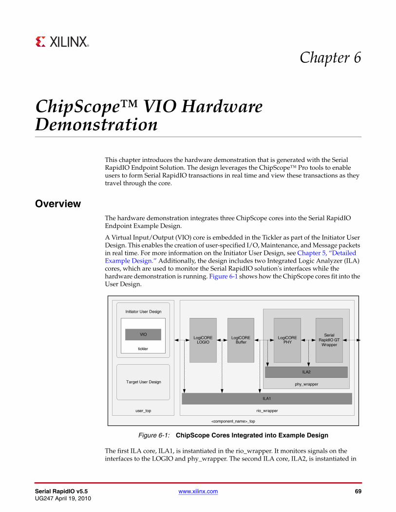
Serial RapidIO v5.5 www.xilinx.com 69UG247 April 19, 2010
Chapter 6
ChipScope™ VIO Hardware Demonstration
This chapter introduces the hardware demonstration that is generated with the Serial RapidIO Endpoint Solution. The design leverages the ChipScope™ Pro tools to enable users to form Serial RapidIO transactions in real time and view these transactions as they travel through the core.
OverviewThe hardware demonstration integrates three ChipScope cores into the Serial RapidIO Endpoint Example Design.
A Virtual Input/Output (VIO) core is embedded in the Tickler as part of the Initiator User Design. This enables the creation of user-specified I/O, Maintenance, and Message packets in real time. For more information on the Initiator User Design, see Chapter 5, “Detailed Example Design.” Additionally, the design includes two Integrated Logic Analyzer (ILA) cores, which are used to monitor the Serial RapidIO solution's interfaces while the hardware demonstration is running. Figure 6-1 shows how the ChipScope cores fit into the User Design.
The first ILA core, ILA1, is instantiated in the rio_wrapper. It monitors signals on the interfaces to the LOGIO and phy_wrapper. The second ILA core, ILA2, is instantiated in
X-Ref Target - Figure 6-1
Figure 6-1: ChipScope Cores Integrated into Example Design
<component_name>_top
phy_wrapper
LogiCORE PHY
rio_wrapper
Serial RapidIO GT
Wrapper
LogiCORE LOGIO
LogiCOREBuffer
ILA1
ILA2
user_top
Initiator User Design
Target User Design
tickler
VIO
70 www.xilinx.com Serial RapidIO v5.5UG247 April 19, 2010
Chapter 6: ChipScope™ VIO Hardware Demonstration
the phy_wrapper and monitors the interfaces to the PHY. For a full listing of VIO and ILA signals, see “ChipScope Core Signals,” page 72.
Tools Required
Hardware• Board with a Xilinx Virtex-4, Virtex-5, Virtex-6, or Spartan-6 device that supports the
Serial RapidIO core
♦ Examples include the ML421, ML505, ML523, ML605, ML623 boards
• 6 (x1 core) or 18 (x4 core) SMA Cables (2 for clock and 4 for each lane, unless in loopback)
• Xilinx Platform Cable USB
Software• ISE Design Suite software
• Serial RapidIO Full or Hardware Evaluation license
• ChipScope Pro Analyzer (with same version as ISE)
• ChipScope Pro 30-day Evaluation license or Full license
Generating Hardware Demonstration Files
Generating the CoreSee Chapter 3, “Customizing and Generating the Cores” for instructions on generating the Serial RapidIO core. Key selections dependent on board selection and connections for this demonstration are Lane Width, Transfer Frequency, and Input Clock Frequency (see Figure 3-2, page 24). Take note of the selected Component Device ID (see Figure 3-3, page 26). The Master Enable bit must be selected for the VIO Demo (see Figure 3-8, page 36).
Enabling ChipScope in Serial RapidIO SolutionAll Serial RapidIO cores are automatically generated with the necessary ChipScope cores inserted into the Example Design.
For Virtex-4 devices, the user must manually change the value of the SRIO_VIO parameter in the <component_name>_top.v[hd] file to '1.'
UCF ModificationsThe User Constraints File (UCF) generated with the core is pre-targeted to specific Xilinx development boards based on the device selected in CORE Generator:
• Virtex-4: Generated UCF has pinout for ML421.
• Virtex-5: UCF has pinout for ML523 (with a XC5VLX50T-FF1136 device).

Serial RapidIO v5.5 www.xilinx.com 71UG247 April 19, 2010
Hardware Setup
If targeting the ML523 board, you must use the ML523 RevD or later board. The UCF needs modification to target a Virtex-5 LX110T device. The CONFIG PART line and the MGT locations will need to be changed as follows for the Virtex-5 LX110T:
CONFIG PART = XC5VLX110T-FF1136-1 ;
INST "rio_de_wrapper/phy_wrapper/rocketio_wrapper/gtp_wrapper/tile1_gtp_wrapper_i/gtp_dual_i" LOC = "GTP_DUAL_X0Y4";# MGT112
INST "rio_de_wrapper/phy_wrapper/rocketio_wrapper/gtp_wrapper/tile0_gtp_wrapper_i/gtp_dual_i" LOC = "GTP_DUAL_X0Y3";# MGT114
• Virtex-5: With x1 lane selected and Component Name beginning with "ml505_" (for example, "ml505_demo"), UCF has pinout for ML505.
• Virtex-6: UCF has pinout for ML623 (with a XC6VLX420T-FF1156 device).
Creating a Bit FileOnce any necessary modifications to the UCF file are made, the design can be implemented to produce a bit file for use in hardware. See the “Implementing the Example Design” in Chapter 4 for details.
ChipScope Project FileThe file containing ChipScope Analyzer project information, srio.cpj, includes signal/bus naming and trigger condition information. The file is located in:
<srio_component_name>/example_design/chipscope/
This file is specifically used to target Xilinx development boards, so it may not work properly for other boards. Specifically, the signal names may not be imported because the JTAG chain settings may be incorrect. For third-party boards, see the “ChipScope Core Signals,” page 72 and manually name the signals in ChipScope Analyzer.
Hardware SetupSince the user design is set up to implement basic RapidIO Endpoint functionality, the hardware demonstration can be set up in a variety of ways.
LoopbackThe simplest hardware setup involves looping back the core's transmitter to its receiver. For a 1x core, the transmitter of lane 0 should be connected to the lane 0 receiver. For a 4x core, the hardware demo can be run in 1x mode (by placing only one lane in loopback and leaving the others unconnected) or by connecting the transmitter of each of the 4 lanes to its respective receiver. In the case of Xilinx Development Boards, SMA cables are typically used to make the loopback connection.
Chip-to-ChipFor a more elaborate test, the Xilinx Serial RapidIO solution can be connected to another Serial RapidIO Endpoint. The Register Manager and the Target User Design will handle

72 www.xilinx.com Serial RapidIO v5.5UG247 April 19, 2010
Chapter 6: ChipScope™ VIO Hardware Demonstration
incoming transactions, and the VIO-based hardware demo can be used to initiate transactions targeted to the local configuration space or to the remote endpoint.
Connecting to a SwitchThe Xilinx Serial RapidIO solution with hardware demonstration enabled can be connected to a RapidIO-based system via a switch. In systems of this type, it is important to use the appropriate Destination ID for transactions initiated from the VIO interface. The switch may require certain configuration transactions in order to communicate with the endpoint.
This setup can be useful for verifying that the core's configuration is valid before adding in a custom user design.
ChipScope Core Signals
VIO Core SignalsThe VIO core allows the user to create transactions that the Initiator User Design will send into the Serial RapidIO core. In ChipScope Analyzer, the user will select which transaction types will be generated, then set parameters such as the number of transactions, Destination ID, and transaction priority. The VIO Input signals are updated each time ChipScope Analyzer scans the JTAG chain. The Analyzer then provides a snapshot of the signals at the time of the scan.
Table 6-1: VIO Output Signals
VIO Alias Signal NamePort
Number(s)Description
Reinit vio_reinit 184 See description of force_reinit in “Core Architecture” in UG503, LogiCORE IP Serial RapidIO User Guide.
TResp_Stallsa vio_tresp_stalls[0:1] 183:182 Currently unsupported.
IResp_Stallsa vio_iresp_stalls[0:1] 181:180 Currently unsupported.
RandomizeSizea vio_rand_size 179 Set to '1' to randomize the length for each transaction for which a length change is valid. Set to '0' to use the vio_size[0:16] input.
RandomizePrioa vio_rand_prio 178 Set to '1' to randomize the priority for each transaction for which the priority field is applicable. Set to '0' to use the vio_prio[0:1] input.
BurstSize vio_burst_size[0:5] 177:172 Number of times each transaction is run before switching to a new transaction.
ErrorEnablea vio_error_enable[0:7] 171:164 Currently unsupported.
DestId vio_dest_id[0:15] 163:148 Drives igen_dest_id, see Table 5-13, page 63.
MsgSega vio_msgseg[0:3] 147:144 Drives igen_msgseg, see Table 5-13, page 63.
Mailboxa vio_mbox[0:1] 143:142 Drives igen_mbox, see Table 5-13, page 63.
Lettera vio_letter[0:1] 141:140 Drives igen_letter, see Table 5-13, page 63.
MSGLena vio_msglen[0:3] 139:136 Drives igen_msglen, see Table 5-13, page 63.

Serial RapidIO v5.5 www.xilinx.com 73UG247 April 19, 2010
ChipScope Core Signals
DBInfo vio_db_info[0:15] 135:120 Drives igen_db_info, see Table 5-13, page 63.
Locala vio_local 119 Drives igen_local, see Table 5-13, page 63.
Hopcount vio_hopcount[0:7] 118:111 Drives igen_hopcount, seeTable 5-13, page 63.
CRFa vio_crf 110 Drives igen_crf, see Table 5-13, page 63.
Prioa vio_prio[0:1] 109:108 Drives igen_prio when vio_rand_prio is '0'. The igen_prio signal is documented in Table 5-13, page 63.
BypassEnable vio_bypass_en 107 Drives igen_bypass_en, see Table 5-13, page 63.
BypassData vio_bypass_data[0:31] 106:75 Drives igen_bypass_data, see Table 5-13, page 63.
BlockSizea vio_blk_size[0:16] 74:58 Indicates the size of the addressable space available for writing and reading. Indirectly determines the maximum value to be used for the addresses in a set of transaction cycles (sequences). If the address increments past the vio_start_addr plus the vio_blk_size, it will wrap back around to the start address.
Start_Addr vio_start_addr[0:33] 57:24 Sets the start address for I/O transactions. For the first sequence, each burst of selected transaction types will use the same start address. For each subsequent sequence (transaction cycle), each transaction type will begin at the vio_burst_size times vio_size plus vio_start_addr.
Stallsa vio_stalls[0:1] 23:22 Currently unsupported.
Num_Seq vio_num_seq[0:3] 21:18 Sequences are made up of a series of transactions. Once a transaction cycle is complete (every selected transaction has been run the number of times specified by the burst_size), a new transaction cycle will begin unless the specified number of sequences has been run. A value of 'F' for this input will tell the core to run for infinite transaction cycles.
Size vio_size[0:8] 17:9 Drives igen_size when vio_rand_size is '0'. The igen_size signal is documented in Table 5-13, page 63.
Maint_Rd vio_maint_rd 8 Indicates that MAINTENANCE READ transactions will be generated (number to be determined by vio_burst_size and vio_num_seq).
Maint_Wrt vio_maint_wrt 7 Indicates that MAINTENANCE WRITE transactions will be generated (number to be determined by vio_burst_size and vio_num_seq).
Doorbell vio_db 6 Indicates that DOORBELL transactions will be generated (number to be determined by vio_burst_size and vio_num_seq).
Message vio_msg 5 Indicates that MESSAGE transactions will be generated (number to be determined by vio_burst_size and vio_num_seq).
NRead vio_nread 4 Indicates that NREAD transactions will be generated (number to be determined by vio_burst_size and vio_num_seq).
Table 6-1: VIO Output Signals (Cont’d)
VIO Alias Signal NamePort
Number(s)Description

74 www.xilinx.com Serial RapidIO v5.5UG247 April 19, 2010
Chapter 6: ChipScope™ VIO Hardware Demonstration
SWrite vio_swrite 3 Indicates that SWRITE transactions will be generated (number to be determined by vio_burst_size and vio_num_seq).
NWrite_R vio_nwrite_r 2 Indicates that NWRITE transactions will be generated (number to be determined by vio_burst_size and vio_num_seq).
NWrite vio_nwrite 1 Indicates that NWRITE_R transactions will be generated (number to be determined by vio_burst_size and vio_num_seq).
GO vio_go 0 On the rising edge of GO, the tickler will start sending transactions. If vio_num_seq is set such that the tickler will produce infinite transactions, transactions will be sent for as long as GO is '1'. When GO is '0,' no transactions are generated.
a. Not in VIO Console by default. Can be added for advanced control.
Table 6-1: VIO Output Signals (Cont’d)
VIO Alias Signal NamePort
Number(s)Description
Table 6-2: VIO Input Signals
VIO Alias Signal NamePort
Number(s)Description
iresp_sof q_sof 127 Validated IRESP start-of-frame. The q_sof signal in the Initiator Response Handler is active-high and asserts when iresp_sof_n, iresp_rdy_n, and iresp_vld_n are all asserted. See “Core Architecture” in UG503, LogiCORE IP Serial RapidIO User Guide, for the description of IRESP interface signals.
iresp_eof q_eof 126 Validated IRESP end-of-frame. The q_eof signal in the Initiator Response Handler is active-high and asserts when iresp_eof_n, iresp_rdy_n, and iresp_vld_n are all asserted. See “Core Architecture” in UG503, LogiCORE IP Serial RapidIO User Guide, for the description of IRESP interface signals.
iresp_vld q_vld 125 Validated IRESP valid signal. The q_vld signal in the Initiator Response Handler is active-high and updates to the inverse of iresp_vld_n when iresp_rdy_n is asserted. See “Core Architecture” in UG503, LogiCORE IP Serial RapidIO User Guide, for the description of IRESP interface signals.
iresp_rdy_n iresp_rdy_n 124 See “Core Architecture” in UG503, LogiCORE IP Serial RapidIO User Guide, for the description of this signal.
iresp_dataa first_data[0:63] 123:60 This signal stores the first eight bytes of a packet on the IRESP interface and updates with each new packet.
iresp_ftypea q_ftype[0:3] 59:56 Validated IRESP FTYPE. The q_ftype signal in the Initiator Response Handler is updated to the current iresp_ftype when iresp_sof_n, iresp_rdy_n, and iresp_vld_n are all asserted. See “Core Architecture” in UG503, LogiCORE IP Serial RapidIO User Guide, for the description of IRESP interface signals.

Serial RapidIO v5.5 www.xilinx.com 75UG247 April 19, 2010
ChipScope Core Signals
iresp_ttypea q_ttype[0:3] 55:52 Validated IRESP TTYPE. The q_ttype signal in the Initiator Response Handler is updated to the current iresp_ttype when iresp_sof_n, iresp_rdy_n, and iresp_vld_n are all asserted. See “Core Architecture” in UG503, LogiCORE IP Serial RapidIO User Guide, for the description of IRESP interface signals.
iresp_status q_status[0:3] 51:48 Validated IRESP Status. The q_status signal in the Initiator Response Handler is updated to the current iresp_status when iresp_sof_n, iresp_rdy_n, and iresp_vld_n are all asserted. See “Core Architecture” in UG503, LogiCORE IP Serial RapidIO User Guide, for the description of IRESP interface signals.
iresp_tid q_tid[0:7] 47:40 Validated IRESP TID. The q_tid signal in the Initiator Response Handler is updated to the current iresp_tid when iresp_sof_n, iresp_rdy_n, and iresp_vld_n are all asserted. See “Core Architecture” in UG503, LogiCORE IP Serial RapidIO User Guide, for the description of IRESP interface signals.
iresp_msg_sega q_msg_seg[0:3] 39:36 Validated IRESP Message Segment. The q_msg_seg signal in the Initiator Response Handler is updated to the current iresp_msg_seg when iresp_sof_n, iresp_rdy_n, and iresp_vld_n are all asserted. See “Core Architecture” in UG503, LogiCORE IP Serial RapidIO User Guide, for the description of IRESP interface signals.
iresp_mboxa q_mbox[0:1] 35:34 Validated IRESP Mailbox. The q_mbox signal in the Initiator Response Handler is updated to the current iresp_mbox when iresp_sof_n, iresp_rdy_n, and iresp_vld_n are all asserted. See “Core Architecture” in UG503, LogiCORE IP Serial RapidIO User Guide, for the description of IRESP interface signals.
iresp_lettera q_letter[0:1] 33:32 Validated IRESP Letter. The q_letter signal in the Initiator Response Handler is updated to the current iresp_letter when iresp_sof_n, iresp_rdy_n, and iresp_vld_n are all asserted. See “Core Architecture” in UG503, LogiCORE IP Serial RapidIO User Guide, for the description of IRESP interface signals.
ireq_sof_n ireq_sof_n 31 See “Core Architecture” in UG503, LogiCORE IP Serial RapidIO User Guide, for the description of this signal.
ireq_eof_n ireq_eof_n 30 See “Core Architecture” in UG503, LogiCORE IP Serial RapidIO User Guide, for the description of this signal.
ireq_vld_n ireq_vld_n 29 See “Core Architecture” in UG503, LogiCORE IP Serial RapidIO User Guide, for the description of this signal.
ireq_rdy_n ireq_rdy_n 28 See “Core Architecture” in UG503, LogiCORE IP Serial RapidIO User Guide, for the description of this signal.
ireq_tid ireq_tid[0:7] 27:20 See “Core Architecture” in UG503, LogiCORE IP Serial RapidIO User Guide, for the description of this signal.
ireq_ftypea ireq_ftype[0:3] 19:16 See “Core Architecture” in UG503, LogiCORE IP Serial RapidIO User Guide, for the description of this signal.
ireq_ttypea ireq_ttype[0:3] 15:12 See “Core Architecture” in UG503, LogiCORE IP Serial RapidIO User Guide, for the description of this signal.
Table 6-2: VIO Input Signals (Cont’d)
VIO Alias Signal NamePort
Number(s)Description

76 www.xilinx.com Serial RapidIO v5.5UG247 April 19, 2010
Chapter 6: ChipScope™ VIO Hardware Demonstration
ILA SignalsThe two ILA cores act as logic analyzers within the FPGA. They store data in the block RAM of the FPGA until the ChipScope software can read it out over the JTAG connection. ChipScope Analyzer is then used to display the captured data as a waveform. Table 6-3 and Table 6-4 list the signals that are present in the ILA cores.
Both ILA cores use uclk to sample data. ILA1 allows packet tracking through the core. The default trigger condition for ILA1 is the simultaneous assertion of ireq_sof_n and ireq_vld_n.
ireq_dest_ida ireq_dest_id[0:7] 11:4 See “Core Architecture” in UG503, LogiCORE IP Serial RapidIO User Guide, for the description of this signal.
ireq_hopcounta ireq_hopcount[6:7] 3:2 See “Core Architecture” in UG503, LogiCORE IP Serial RapidIO User Guide, for the description of this signal.
ireq_local ireq_local 1 See “Core Architecture” in UG503, LogiCORE IP Serial RapidIO User Guide, for the description of this signal.
tickler_errora tickler_error 0 Currently unsupported.
a. Not in VIO Console by default. Can be added for advanced monitoring.
Table 6-2: VIO Input Signals (Cont’d)
VIO Alias Signal NamePort
Number(s)Description
Table 6-3: ILA1 Signals
Signal NameData Port
Number(s)Trigger PortNumber(s)
Type Description
target_error 255 0 Not Supported Currently unsupported.
ireq_sof_n 254 31 Active Low See “Core Architecture” in UG503, LogiCORE IP Serial RapidIO User Guide, for the description of this signal.
ireq_eof_n 253 -- Active Low See “Core Architecture” in UG503, LogiCORE IP Serial RapidIO User Guide, for the description of this signal.
ireq_vld_n 252 30 Active Low See “Core Architecture” in UG503, LogiCORE IP Serial RapidIO User Guide, for the description of this signal.
ireq_rdy_n 251 29 Active Low See “Core Architecture” in UG503, LogiCORE IP Serial RapidIO User Guide, for the description of this signal.
ireq_ftype[0:3] 250:247 -- See “Core Architecture” in UG503, LogiCORE IP Serial RapidIO User Guide, for the description of this signal.
ireq_ttype[0:3] 246:243 -- See “Core Architecture” in UG503, LogiCORE IP Serial RapidIO User Guide, for the description of this signal.
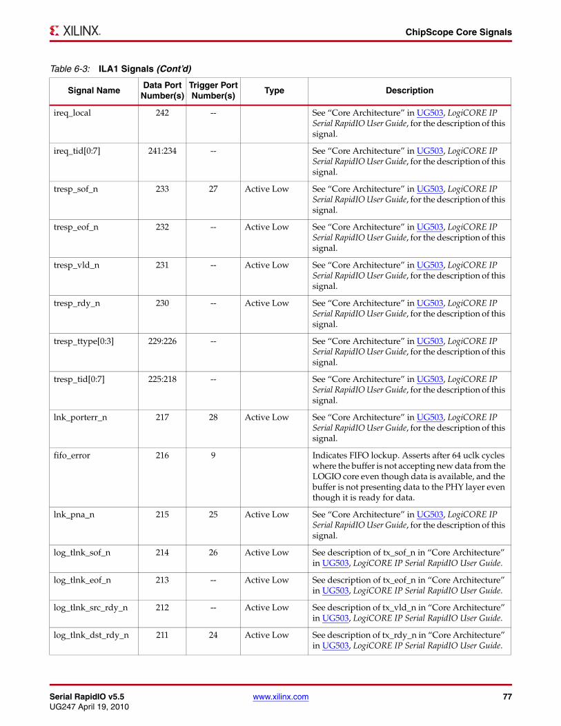
Serial RapidIO v5.5 www.xilinx.com 77UG247 April 19, 2010
ChipScope Core Signals
ireq_local 242 -- See “Core Architecture” in UG503, LogiCORE IP Serial RapidIO User Guide, for the description of this signal.
ireq_tid[0:7] 241:234 -- See “Core Architecture” in UG503, LogiCORE IP Serial RapidIO User Guide, for the description of this signal.
tresp_sof_n 233 27 Active Low See “Core Architecture” in UG503, LogiCORE IP Serial RapidIO User Guide, for the description of this signal.
tresp_eof_n 232 -- Active Low See “Core Architecture” in UG503, LogiCORE IP Serial RapidIO User Guide, for the description of this signal.
tresp_vld_n 231 -- Active Low See “Core Architecture” in UG503, LogiCORE IP Serial RapidIO User Guide, for the description of this signal.
tresp_rdy_n 230 -- Active Low See “Core Architecture” in UG503, LogiCORE IP Serial RapidIO User Guide, for the description of this signal.
tresp_ttype[0:3] 229:226 -- See “Core Architecture” in UG503, LogiCORE IP Serial RapidIO User Guide, for the description of this signal.
tresp_tid[0:7] 225:218 -- See “Core Architecture” in UG503, LogiCORE IP Serial RapidIO User Guide, for the description of this signal.
lnk_porterr_n 217 28 Active Low See “Core Architecture” in UG503, LogiCORE IP Serial RapidIO User Guide, for the description of this signal.
fifo_error 216 9 Indicates FIFO lockup. Asserts after 64 uclk cycles where the buffer is not accepting new data from the LOGIO core even though data is available, and the buffer is not presenting data to the PHY layer even though it is ready for data.
lnk_pna_n 215 25 Active Low See “Core Architecture” in UG503, LogiCORE IP Serial RapidIO User Guide, for the description of this signal.
log_tlnk_sof_n 214 26 Active Low See description of tx_sof_n in “Core Architecture” in UG503, LogiCORE IP Serial RapidIO User Guide.
log_tlnk_eof_n 213 -- Active Low See description of tx_eof_n in “Core Architecture” in UG503, LogiCORE IP Serial RapidIO User Guide.
log_tlnk_src_rdy_n 212 -- Active Low See description of tx_vld_n in “Core Architecture” in UG503, LogiCORE IP Serial RapidIO User Guide.
log_tlnk_dst_rdy_n 211 24 Active Low See description of tx_rdy_n in “Core Architecture” in UG503, LogiCORE IP Serial RapidIO User Guide.
Table 6-3: ILA1 Signals (Cont’d)
Signal NameData Port
Number(s)Trigger PortNumber(s)
Type Description

78 www.xilinx.com Serial RapidIO v5.5UG247 April 19, 2010
Chapter 6: ChipScope™ VIO Hardware Demonstration
phy_tlnk_sof_n 210 23 Active Low See description of lnk_tsof_n in “Core Architecture” in UG503, LogiCORE IP Serial RapidIO User Guide.
phy_tlnk_eof_n 209 22 Active Low See description of lnk_teof_n in “Core Architecture” in UG503, LogiCORE IP Serial RapidIO User Guide.
phy_tlnk_src_rdy_n 208 21 Active Low See description of lnk_tsrc_rdy_n in “Core Architecture” in UG503, LogiCORE IP Serial RapidIO User Guide.
phy_tlnk_src_dsc_n 207 20 Active Low See description of lnk_tsrc_dsc_n in “Core Architecture” in UG503, LogiCORE IP Serial RapidIO User Guide.
phy_tlnk_dst_rdy_n 206 19 Active Low See description of lnk_tdst_rdy_n in “Core Architecture” in UG503, LogiCORE IP Serial RapidIO User Guide.
phy_tlnk_dst_dsc_n 205 18 Active Low See description of lnk_tdst_dsc_n in “Core Architecture” in UG503, LogiCORE IP Serial RapidIO User Guide.
phy_tlnk_d[0:63] 204:141 -- See description of lnk_td in “Core Architecture” in UG503, LogiCORE IP Serial RapidIO User Guide.
phy_tlnk_rem[0:2] 140:138 -- See description of lnk_trem in “Core Architecture” in UG503, LogiCORE IP Serial RapidIO User Guide.
lnk_tnext_fm[0:4] 137:133 -- See description of tx_vld_n in “Core Architecture” in UG503, LogiCORE IP Serial RapidIO User Guide.
lnk_tnext_ack[0:4] 132:128 -- See description of tx_vld_n in “Core Architecture” in UG503, LogiCORE IP Serial RapidIO User Guide.
phy_rlnk_sof_n 127 17 Active Low See description of lnk_rsof_n in “Core Architecture” in UG503, LogiCORE IP Serial RapidIO User Guide.
phy_rlnk_eof_n 126 16 Active Low See description of lnk_reof_n in “Core Architecture” in UG503, LogiCORE IP Serial RapidIO User Guide.
phy_rlnk_dst_rdy_n 125 15 Active Low See description of lnk_rdst_rdy_n in “Core Architecture” in UG503, LogiCORE IP Serial RapidIO User Guide.
phy_rlnk_dst_dsc_n 124 14 Active Low See description of lnk_rdst_dsc_n in “Core Architecture” in UG503, LogiCORE IP Serial RapidIO User Guide.
phy_rlnk_src_rdy_n 123 13 Active Low See description of lnk_rsrc_rdy_n in “Core Architecture” in UG503, LogiCORE IP Serial RapidIO User Guide.
Table 6-3: ILA1 Signals (Cont’d)
Signal NameData Port
Number(s)Trigger PortNumber(s)
Type Description

Serial RapidIO v5.5 www.xilinx.com 79UG247 April 19, 2010
ChipScope Core Signals
phy_rlnk_src_dsc_n 122 12 Active Low See description of lnk_rsrc_dsc_n in “Core Architecture” in UG503, LogiCORE IP Serial RapidIO User Guide.
phy_rlnk_d[0:63] 121:58 -- See description of lnk_rd in “Core Architecture” in UG503, LogiCORE IP Serial RapidIO User Guide.
phy_rlnk_rem[0:2] 57:55 -- See description of lnk_rrem in “Core Architecture” in UG503, LogiCORE IP Serial RapidIO User Guide.
log_rlnk_sof_n 54 -- Active Low See description of rx_sof_n in “Core Architecture” in UG503, LogiCORE IP Serial RapidIO User Guide.
log_rlnk_eof_n 53 -- Active Low See description of rx_eof_n in “Core Architecture” in UG503, LogiCORE IP Serial RapidIO User Guide.
log_rlnk_src_rdy_n 52 -- Active Low See description of rx_vld_n in “Core Architecture” in UG503, LogiCORE IP Serial RapidIO User Guide.
log_rlnk_dst_rdy_n 51 -- Active Low See description of rx_rdy_n in “Core Architecture” in UG503, LogiCORE IP Serial RapidIO User Guide.
iresp_sof_n 50 10 Active Low See “Core Architecture” in UG503, LogiCORE IP Serial RapidIO User Guide, for the description of this signal.
iresp_eof_n 49 -- Active Low See “Core Architecture” in UG503, LogiCORE IP Serial RapidIO User Guide, for the description of this signal.
iresp_vld_n 48 -- Active Low See “Core Architecture” in UG503, LogiCORE IP Serial RapidIO User Guide, for the description of this signal.
iresp_rdy_n 47 -- Active Low See “Core Architecture” in UG503, LogiCORE IP Serial RapidIO User Guide, for the description of this signal.
iresp_ftype[0:3] 46:43 -- See “Core Architecture” in UG503, LogiCORE IP Serial RapidIO User Guide, for the description of this signal.
iresp_ttype[0:3] 42:39 -- See “Core Architecture” in UG503, LogiCORE IP Serial RapidIO User Guide, for the description of this signal.
iresp_tid[0:7] 38:31 -- See “Core Architecture” in UG503, LogiCORE IP Serial RapidIO User Guide, for the description of this signal.
iresp_status[0:3] 30:27 -- See “Core Architecture” in UG503, LogiCORE IP Serial RapidIO User Guide, for the description of this signal.
treq_sof_n 26 11 Active Low See “Core Architecture” in UG503, LogiCORE IP Serial RapidIO User Guide, for the description of this signal.
Table 6-3: ILA1 Signals (Cont’d)
Signal NameData Port
Number(s)Trigger PortNumber(s)
Type Description

80 www.xilinx.com Serial RapidIO v5.5UG247 April 19, 2010
Chapter 6: ChipScope™ VIO Hardware Demonstration
ILA2 allows analysis of the PHY interface and gives the capability of monitoring traffic on the link. The default trigger condition for ILA2 is the simultaneous assertion of lnk_tsof_n and lnk_tsrc_rdy_n, which indicates that the buffer is presenting start-of-frame information to the phy_wrapper.
treq_eof_n 25 -- Active Low See “Core Architecture” in UG503, LogiCORE IP Serial RapidIO User Guide, for the description of this signal.
treq_vld_n 24 -- Active Low See “Core Architecture” in UG503, LogiCORE IP Serial RapidIO User Guide, for the description of this signal.
treq_rdy_n 23 -- Active Low See “Core Architecture” in UG503, LogiCORE IP Serial RapidIO User Guide, for the description of this signal.
treq_ftype[0:3] 22:19 -- See “Core Architecture” in UG503, LogiCORE IP Serial RapidIO User Guide, for the description of this signal.
treq_ttype[0:3] 18:15 -- See “Core Architecture” in UG503, LogiCORE IP Serial RapidIO User Guide, for the description of this signal.
treq_tid[0:7] 14:7 -- See “Core Architecture” in UG503, LogiCORE IP Serial RapidIO User Guide, for the description of this signal.
h_error[0:7] 6:0 8:1 Not Supported Currently unsupported. Only h_error[1:7] are connected to the ILA's data port.
Table 6-3: ILA1 Signals (Cont’d)
Signal NameData Port
Number(s)Trigger PortNumber(s)
Type Description
Table 6-4: ILA2 Signals
Signal NameData Port
Number(s)aTrigger PortNumber(s)a
Type Description
txdata[0:63] 255:192 -- See “Core Architecture” in UG503, LogiCORE IP Serial RapidIO User Guide, for the description of this signal. Only bits 0:15 of txdata are present in 1x cores.
txcharisk[0:7] 191:184 -- See “Core Architecture” in UG503, LogiCORE IP Serial RapidIO User Guide, for the description of this signal. Only bits 0:1 of txcharisk are present in 1x cores.
rxdata[0:63] 183:120 -- See “Core Architecture” in UG503, LogiCORE IP Serial RapidIO User Guide, for the description of this signal. Only bits 0:15 of rxdata are present in 1x cores.
rxcharisk[0:7] 119:112 -- See “Core Architecture” in UG503, LogiCORE IP Serial RapidIO User Guide, for the description of this signal.Only bits 0:1 of rxcharisk are present in 1x cores.
txinhibit_02 111 6 4x Only See “Core Architecture” in UG503, LogiCORE IP Serial RapidIO User Guide, for the description of this signal.

Serial RapidIO v5.5 www.xilinx.com 81UG247 April 19, 2010
ChipScope Core Signals
txinhibit 111 6 1x Only See “Core Architecture” in UG503, LogiCORE IP Serial RapidIO User Guide, for the description of this signal.
txinhibit_13 110 5 4x Only See “Core Architecture” in UG503, LogiCORE IP Serial RapidIO User Guide, for the description of this signal. Data and trigger ports tied to '1' for 1x cores.
lnk_tsof_n 109 31 Active Low See “Core Architecture” in UG503, LogiCORE IP Serial RapidIO User Guide, for the description of this signal.
lnk_teof_n 108 30 Active Low See “Core Architecture” in UG503, LogiCORE IP Serial RapidIO User Guide, for the description of this signal.
lnk_tsrc_rdy_n 107 29 Active Low See “Core Architecture” in UG503, LogiCORE IP Serial RapidIO User Guide, for the description of this signal.
lnk_tdst_rdy_n 106 28 Active Low See “Core Architecture” in UG503, LogiCORE IP Serial RapidIO User Guide, for the description of this signal.
lnk_tsrc_dsc_n 105 27 Active Low See “Core Architecture” in UG503, LogiCORE IP Serial RapidIO User Guide, for the description of this signal.
lnk_tdst_dsc_n 104 26 Active Low See “Core Architecture” in UG503, LogiCORE IP Serial RapidIO User Guide, for the description of this signal.
lnk_tcrf 103 25 Optional See description of crf_bit_tx in “Core Architecture” in UG503, LogiCORE IP Serial RapidIO User Guide.
lnk_rsof_n 102 24 Active Low See “Core Architecture” in UG503, LogiCORE IP Serial RapidIO User Guide, for the description of this signal.
lnk_reof_n 101 23 Active Low See “Core Architecture” in UG503, LogiCORE IP Serial RapidIO User Guide, for the description of this signal.
lnk_rsrc_rdy_n 100 22 Active Low See “Core Architecture” in UG503, LogiCORE IP Serial RapidIO User Guide, for the description of this signal.
lnk_rdst_rdy_n 99 21 Active Low See “Core Architecture” in UG503, LogiCORE IP Serial RapidIO User Guide, for the description of this signal.
lnk_rsrc_dsc_n 98 20 Active Low See “Core Architecture” in UG503, LogiCORE IP Serial RapidIO User Guide, for the description of this signal.
lnk_rdst_dsc_n 97 19 Active Low See “Core Architecture” in UG503, LogiCORE IP Serial RapidIO User Guide, for the description of this signal.
lnk_rcrf 96 18 Optional See description of crf_bit_rx in “Core Architecture” in UG503, LogiCORE IP Serial RapidIO User Guide.
lnk_tnext_fm[0:4] 95:91 -- See “Core Architecture” in UG503, LogiCORE IP Serial RapidIO User Guide, for the description of this signal.
lnk_tlast_ack[0:4] 90:86 -- See “Core Architecture” in UG503, LogiCORE IP Serial RapidIO User Guide, for the description of this signal.
lnk_porterr_n 85 17 Active Low See “Core Architecture” in UG503, LogiCORE IP Serial RapidIO User Guide, for the description of this signal.
Table 6-4: ILA2 Signals (Cont’d)
Signal NameData Port
Number(s)aTrigger PortNumber(s)a
Type Description

82 www.xilinx.com Serial RapidIO v5.5UG247 April 19, 2010
Chapter 6: ChipScope™ VIO Hardware Demonstration
lnk_pna_n 84 16 Active Low See “Core Architecture” in UG503, LogiCORE IP Serial RapidIO User Guide, for the description of this signal.
tc_error[0:7] 83:76 -- Not Supported Currently unsupported.
h_error[0:7] 75:68 13:8 Not Supported Currently unsupported.
fifo_error 67 7 Active High Indicates FIFO lockup. Asserts after 64 uclk cycles where the buffer is not accepting new data from the LOGIO core even though data is available, and the buffer is not presenting data to the PHY layer even though it is ready for data.
port_initialized 66 2 Active High See “Core Architecture” in UG503, LogiCORE IP Serial RapidIO User Guide, for the description of this signal.
rxdisperr[0:7] 65:58 1 See “Core Architecture” in UG503, LogiCORE IP Serial RapidIO User Guide, for the description of this signal.
Only bits 0:1 of rxdisperr are present in 1x cores. The trigger input is an OR of the bus, so there is only one trigger port reserved for rxdisperr.
rxnotintable[0:7] 57:50 0 See “Core Architecture” in UG503, LogiCORE IP Serial RapidIO User Guide, for the description of this signal.
Only bits 0:1 of rxnotintable are present in 1x cores. The trigger input is an OR of the bus, so there is only one trigger port reserved for rxnotintable.
enchanbond 49 4 See “Core Architecture” in UG503, LogiCORE IP Serial RapidIO User Guide, for the description of this signal.
mode_sel 48 3 See “Core Architecture” in UG503, LogiCORE IP Serial RapidIO User Guide, for the description of this signal.
force_reinit 47 -- Active High See “Core Architecture” in UG503, LogiCORE IP Serial RapidIO User Guide, for the description of this signal.
lnk_trdy_n 46 15 Active Low See “Core Architecture” in UG503, LogiCORE IP Serial RapidIO User Guide, for the description of this signal.
lnk_rrdy_n 45 14 Active Low See “Core Architecture” in UG503, LogiCORE IP Serial RapidIO User Guide, for the description of this signal.
pll_locked 44 -- Active High Indicates that the GT PLL is locked.
a. Data ports 239:192, 189:184, 167:120, 117:112, 49, and 48 and trigger ports 4 and 3 are tied to '0' for 1x cores. Data ports 43:0 are tied to '0' for both 1x and 4x cores.
Table 6-4: ILA2 Signals (Cont’d)
Signal NameData Port
Number(s)aTrigger PortNumber(s)a
Type Description

Serial RapidIO v5.5 www.xilinx.com 83UG247 April 19, 2010
Using ChipScope Analyzer
Using ChipScope AnalyzerAll of the functions described in this section are covered in greater detail in UG029, ChipScope Pro Software and Cores User Guide. This section only covers the basics necessary to run the VIO demo with the Serial RapidIO core.
Loading the Core in AnalyzerTo load the VIO demo in ChipScope Analyzer, the ChipScope Project File must first be loaded. In ChipScope Analyzer, select File -> Open Project… and browse to the example_design/chipscope/ directory. Locate srio.cpj and open it.
With the board powered-on and a USB Platform Cable connected via JTAG, a boundary scan must be performed in ChipScope Analyzer. This is done using the Open Cable/Search JTAG chain button located just below the File menu. The JTAG scan should locate the FPGA on the board and any other devices on the JTAG chain, and show all of the devices in the upper-left window in ChipScope Analyzer.
Next, the demo bitstream must be loaded to the board. Right-click on the FPGA device in the upper-left Project window and select Configure… The window shown in Figure 6-2 will appear. Locate your .bit file, usually in the implement/results/ directory, and select it for the FPGA device. Click OK to load the bitstream.
The ChipScope Analyzer EnvironmentOnce the bitstream is loaded, ChipScope Analyzer should populate with several windows, similar to Figure 6-3. If it does not, the windows may be opened manually by double-clicking on them in the Project window in the upper-left corner. The Project window also lists all other devices on the JTAG chain and the VIO and two ILA cores attached to the
X-Ref Target - Figure 6-2
Figure 6-2: Bitstream Selection and Configuration
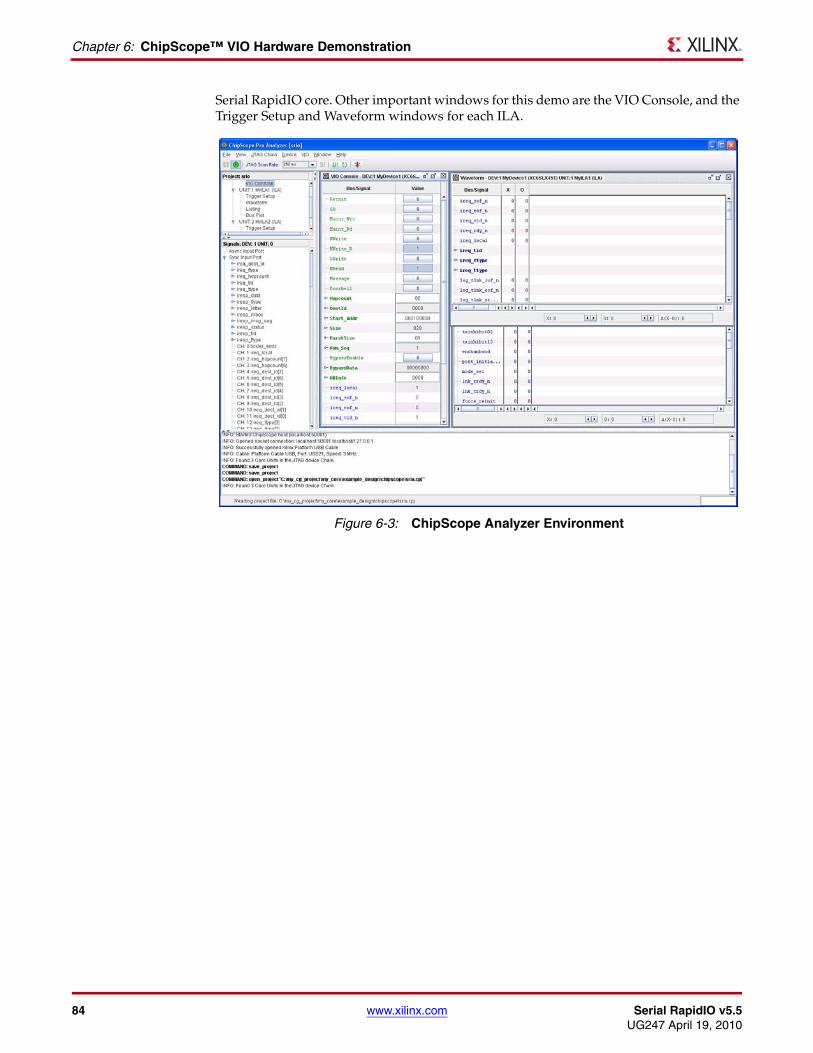
84 www.xilinx.com Serial RapidIO v5.5UG247 April 19, 2010
Chapter 6: ChipScope™ VIO Hardware Demonstration
Serial RapidIO core. Other important windows for this demo are the VIO Console, and the Trigger Setup and Waveform windows for each ILA. X-Ref Target - Figure 6-3
Figure 6-3: ChipScope Analyzer Environment
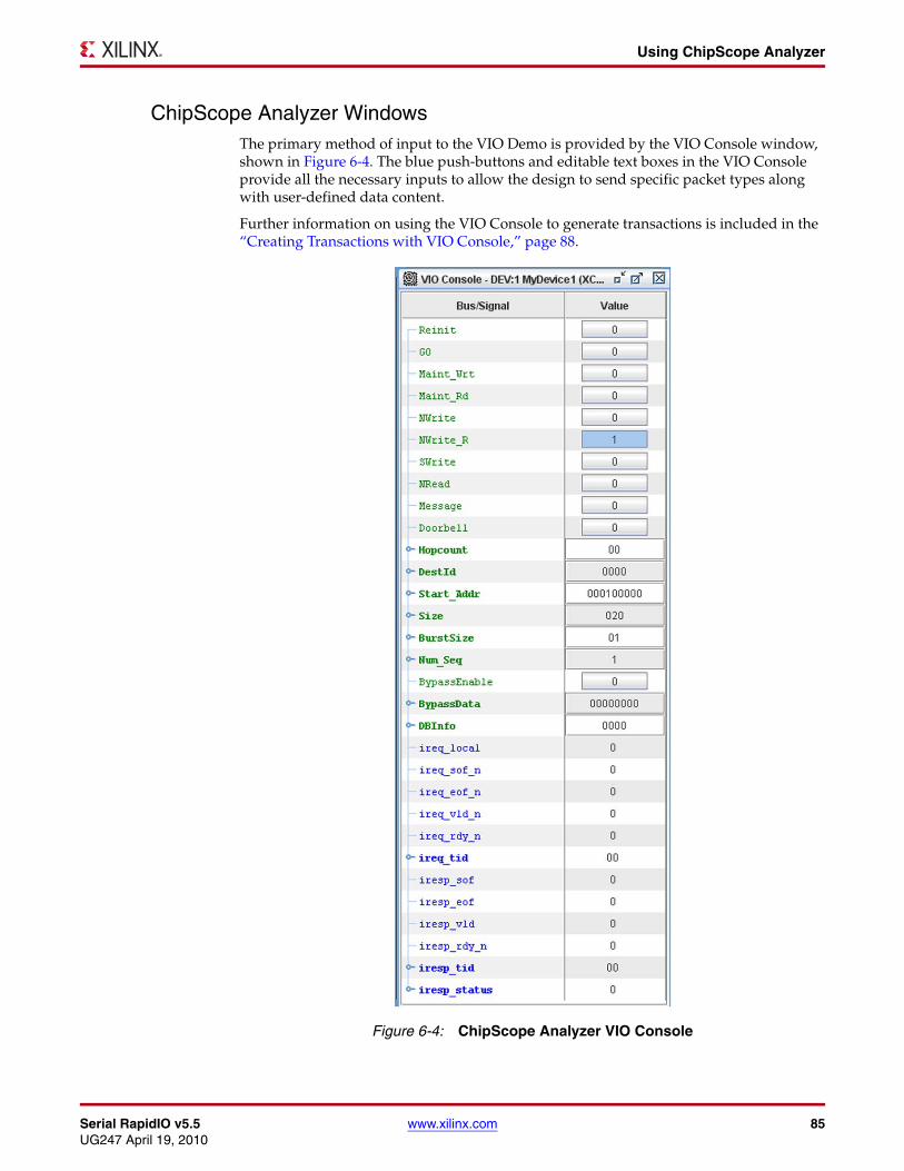
Serial RapidIO v5.5 www.xilinx.com 85UG247 April 19, 2010
Using ChipScope Analyzer
ChipScope Analyzer WindowsThe primary method of input to the VIO Demo is provided by the VIO Console window, shown in Figure 6-4. The blue push-buttons and editable text boxes in the VIO Console provide all the necessary inputs to allow the design to send specific packet types along with user-defined data content.
Further information on using the VIO Console to generate transactions is included in the “Creating Transactions with VIO Console,” page 88.X-Ref Target - Figure 6-4
Figure 6-4: ChipScope Analyzer VIO Console
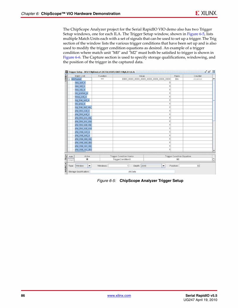
86 www.xilinx.com Serial RapidIO v5.5UG247 April 19, 2010
Chapter 6: ChipScope™ VIO Hardware Demonstration
The ChipScope Analyzer project for the Serial RapidIO VIO demo also has two Trigger Setup windows, one for each ILA. The Trigger Setup window, shown in Figure 6-5, lists multiple Match Units each with a set of signals that can be used to set up a trigger. The Trig section of the window lists the various trigger conditions that have been set up and is also used to modify the trigger condition equations as desired. An example of a trigger condition where match unit "M0" and "M2" must both be satisfied to trigger is shown in Figure 6-6. The Capture section is used to specify storage qualifications, windowing, and the position of the trigger in the captured data.X-Ref Target - Figure 6-5
Figure 6-5: ChipScope Analyzer Trigger Setup

Serial RapidIO v5.5 www.xilinx.com 87UG247 April 19, 2010
Using ChipScope Analyzer
X-Ref Target - Figure 6-6
Figure 6-6: ChipScope Analyzer Trigger Condition Window

88 www.xilinx.com Serial RapidIO v5.5UG247 April 19, 2010
Chapter 6: ChipScope™ VIO Hardware Demonstration
Each Trigger window is associated with a Waveform window. Once a capture takes place, the waveform window for each ILA will populate based on the trigger conditions set for it. Figure 6-7 shows an example of a populated waveform window.
Creating Transactions with VIO ConsoleThe VIO Console can be used to generate the following transaction types:
• MAINTENANCE READ
• MAINTENANCE WRITE
• NWRITE
• NWRITE_R
• SWRITE
• NREAD
• MESSAGE
• DOORBELL
X-Ref Target - Figure 6-7
Figure 6-7: ChipScope Analyzer Waveform Window

Serial RapidIO v5.5 www.xilinx.com 89UG247 April 19, 2010
Creating Transactions with VIO Console
Tips for Creating Serial RapidIO TransactionsThe basic steps for creating transactions using the VIO Console are to:
1. Enable the desired transaction types by setting them to '1.'
2. Modify transaction settings (address, size, etc.) relevant to the selected transaction types.
3. Set GO to '1' to initiate the transactions.
The following tips provide the basic information needed to create a transaction. See “ChipScope Core Signals,” page 72 for more details on signals available for control and monitoring.
Data
When BypassEnable is '1', the data used for an I/O write or MESSAGE transaction will be set by the BypassData field. These four bytes of data will be repeated as necessary to create a transaction of the specified size. If BypassEnable is set to '0', data from the Initiator block RAM will be used.
Addressing
The Start_Addr field in the VIO is used for two purposes. If BypassEnable is '0', the Start_Addr is used to select the data from the Initiator block RAM for I/O write or MESSAGE transactions. In addition, Start_Addr is the address used for outgoing I/O transactions, and is inserted into the config_offset field for outgoing Maintenance transactions.
To issue a transaction to the local endpoint, change the Local output to '1' (Local may first need to be added to the VIO Console). To send transactions to the link partner, set Local to '0'.
For Xilinx cores running the example design, the Initiator and Target block RAM uses an address offset of 0x10_0000. The block RAM is pre-loaded with test values as described in Table 5-12, page 62. Most Reads and Writes targeting the Xilinx example design should use the address space corresponding to that block RAM. Maintenance transactions sent to the Xilinx core should use an offset of 0x00_0000 plus the offset for the layer targeted (e.g., 0x00_0100 for the PHY configuration space), plus the byte offset for the target CAR or CSR.
For example, to read the Port Error and Status CSR in the PHY configuration space, the PHY offset of 0x00_0100 is added to the CSR's byte offset of 0x00_0058; therefore the value of 0x00_0158 should be used for Start_Addr.
The three least significant bits of Start_Addr[31:33] should always be '0'. Sub-dword addressing is relayed through the rdsize and wdptr RapidIO packet fields and presented to the user through the treq_byte_count and treq_byte_en_n signals.
Randomization
There are two VIO outputs which can be used to randomize the transactions. If RandomizePrio or RandomizeSize are set, the values of Size and Prio will be ignored.

90 www.xilinx.com Serial RapidIO v5.5UG247 April 19, 2010
Chapter 6: ChipScope™ VIO Hardware Demonstration
I/O Transaction ExampleThe VIO core is preset to send an NWRITE_R transaction followed by an NREAD transaction. Figure 6-8 shows the VIO Console with the default settings.
First, arm one or both of the ILA cores by opening up the ILA waveform (double-click waveform under selected ILA in Project window), and then selecting Run from the Trigger Setup drop-down menu. Next, set GO to '1' in the VIO Console.
When the trigger is detected by the ILA core, ChipScope will download the data from the FPGA through the JTAG cable, and the ILA waveform will populate with the sampled data.
Interpreting Results of I/O TransactionsThe ILA1 trigger is preset to capture the first simultaneous assertion of ireq_sof_n and ireq_vld_n (the first transfer of packet data into the LOGIO core). It will save data starting 50 cycles before the trigger event, and record 2048 cycles total. With the ILA1 data, the transaction can be seen at the input to the LOGIO (ireq_*), the output of the LOGIO (log_tlnk_*) and the input to the phy_wrapper (phy_tlnk_*). If the core is in loopback, the transaction can also be seen on the receive side, starting with the output from
X-Ref Target - Figure 6-8
Figure 6-8: Default VIO Settings that Produce NWRITE_R and NREAD
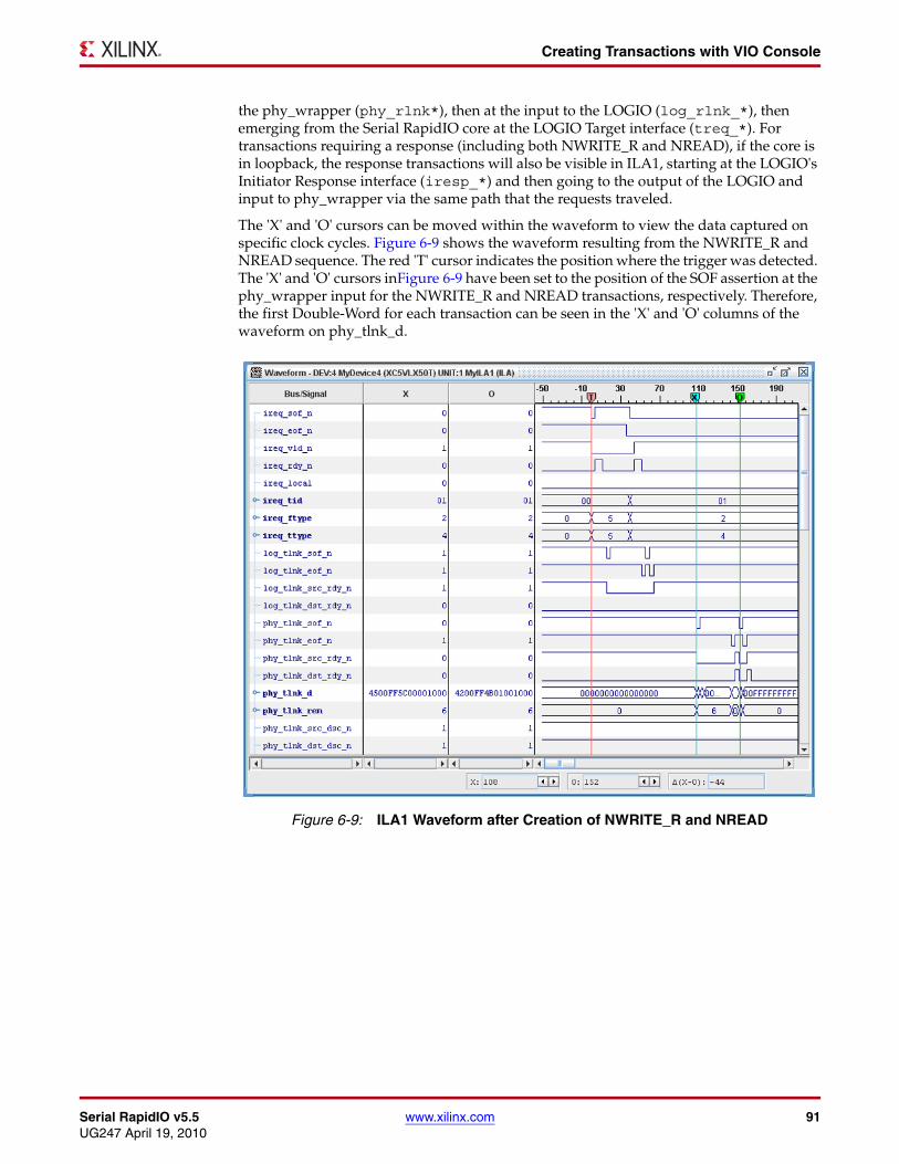
Serial RapidIO v5.5 www.xilinx.com 91UG247 April 19, 2010
Creating Transactions with VIO Console
the phy_wrapper (phy_rlnk*), then at the input to the LOGIO (log_rlnk_*), then emerging from the Serial RapidIO core at the LOGIO Target interface (treq_*). For transactions requiring a response (including both NWRITE_R and NREAD), if the core is in loopback, the response transactions will also be visible in ILA1, starting at the LOGIO's Initiator Response interface (iresp_*) and then going to the output of the LOGIO and input to phy_wrapper via the same path that the requests traveled.
The 'X' and 'O' cursors can be moved within the waveform to view the data captured on specific clock cycles. Figure 6-9 shows the waveform resulting from the NWRITE_R and NREAD sequence. The red 'T' cursor indicates the position where the trigger was detected. The 'X' and 'O' cursors inFigure 6-9 have been set to the position of the SOF assertion at the phy_wrapper input for the NWRITE_R and NREAD transactions, respectively. Therefore, the first Double-Word for each transaction can be seen in the 'X' and 'O' columns of the waveform on phy_tlnk_d.X-Ref Target - Figure 6-9
Figure 6-9: ILA1 Waveform after Creation of NWRITE_R and NREAD
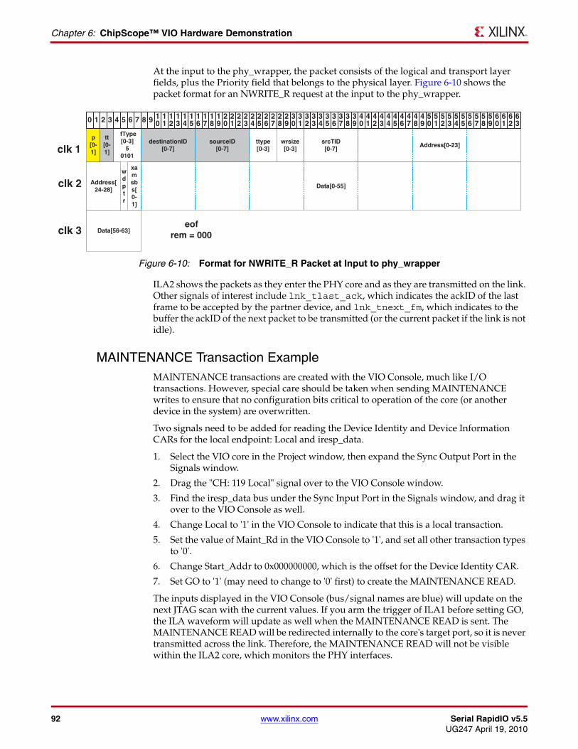
92 www.xilinx.com Serial RapidIO v5.5UG247 April 19, 2010
Chapter 6: ChipScope™ VIO Hardware Demonstration
At the input to the phy_wrapper, the packet consists of the logical and transport layer fields, plus the Priority field that belongs to the physical layer. Figure 6-10 shows the packet format for an NWRITE_R request at the input to the phy_wrapper.
ILA2 shows the packets as they enter the PHY core and as they are transmitted on the link. Other signals of interest include lnk_tlast_ack, which indicates the ackID of the last frame to be accepted by the partner device, and lnk_tnext_fm, which indicates to the buffer the ackID of the next packet to be transmitted (or the current packet if the link is not idle).
MAINTENANCE Transaction ExampleMAINTENANCE transactions are created with the VIO Console, much like I/O transactions. However, special care should be taken when sending MAINTENANCE writes to ensure that no configuration bits critical to operation of the core (or another device in the system) are overwritten.
Two signals need to be added for reading the Device Identity and Device Information CARs for the local endpoint: Local and iresp_data.
1. Select the VIO core in the Project window, then expand the Sync Output Port in the Signals window.
2. Drag the "CH: 119 Local" signal over to the VIO Console window.
3. Find the iresp_data bus under the Sync Input Port in the Signals window, and drag it over to the VIO Console as well.
4. Change Local to '1' in the VIO Console to indicate that this is a local transaction.
5. Set the value of Maint_Rd in the VIO Console to '1', and set all other transaction types to '0'.
6. Change Start_Addr to 0x000000000, which is the offset for the Device Identity CAR.
7. Set GO to '1' (may need to change to '0' first) to create the MAINTENANCE READ.
The inputs displayed in the VIO Console (bus/signal names are blue) will update on the next JTAG scan with the current values. If you arm the trigger of ILA1 before setting GO, the ILA waveform will update as well when the MAINTENANCE READ is sent. The MAINTENANCE READ will be redirected internally to the core's target port, so it is never transmitted across the link. Therefore, the MAINTENANCE READ will not be visible within the ILA2 core, which monitors the PHY interfaces.
X-Ref Target - Figure 6-10
Figure 6-10: Format for NWRITE_R Packet at Input to phy_wrapper
ttype[0-3]
wrsize[0-3]
Address[0-23]
wdptr
p[0-1]
tt[0-1]
fType[0-3]
50101
Address[24-28]
clk 1
clk 2
destinationID[0-7]
sourceID[0-7]
srcTID[0-7]
xamsbs[0-1]
Data[0-55]
Data[56-63]clk 3eof
rem = 000
0 1 2 3 4 5 6 7 8 9 10
11
12
13
14
15
16
17
18
19
20
21
22
23
24
25
26
27
28
29
30
31
32
33
34
35
36
37
38
39
40
41
42
43
44
45
46
47
48
49
50
51
52
53
54
55
56
57
58
59
60
61
62
63
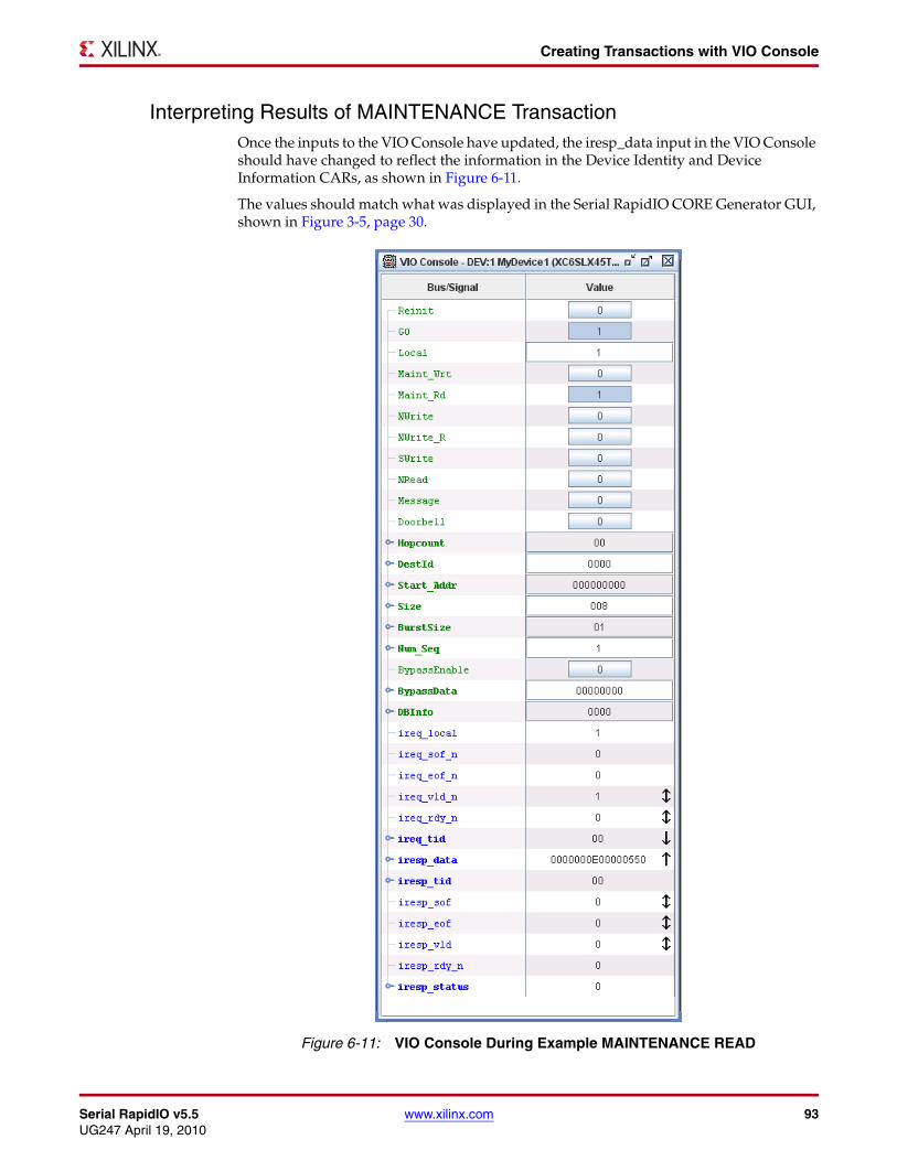
Serial RapidIO v5.5 www.xilinx.com 93UG247 April 19, 2010
Creating Transactions with VIO Console
Interpreting Results of MAINTENANCE TransactionOnce the inputs to the VIO Console have updated, the iresp_data input in the VIO Console should have changed to reflect the information in the Device Identity and Device Information CARs, as shown in Figure 6-11.
The values should match what was displayed in the Serial RapidIO CORE Generator GUI, shown in Figure 3-5, page 30.X-Ref Target - Figure 6-11
Figure 6-11: VIO Console During Example MAINTENANCE READ

94 www.xilinx.com Serial RapidIO v5.5UG247 April 19, 2010
Chapter 6: ChipScope™ VIO Hardware Demonstration
The iresp_data input to the VIO Console will update with the first eight bytes of data of the most recent packet on the IRESP port. The ireq_tid and iresp_tid ports will update with the Transaction ID from the most recent packet on each respective port. See Table 6-1, page 72 for descriptions of the VIO core signals.
For MAINTENANCE transactions targeting remote endpoints, ChipScope can be used to monitor the packet as it travels through the core in the same way that it is used for I/O transactions.