Logic Designcourses.cs.vt.edu/cs2506/Spring2020/notes/DL01_IntroDigitalLogic.pdf · Digital Logic...
32
Digital Logic Computer Organization II 1 CS@VT ©2005-2020 WD McQuain Logic Design Goal: to become literate in most common concepts and terminology of digital electronics Important concepts: - use abstraction and composition to implement complicated functionality with very simple digital electronics - keep things as simple, regular, and small as possible Things we will not explore: - physics - chip fabrication - layout - tools for chip specification and design
Transcript of Logic Designcourses.cs.vt.edu/cs2506/Spring2020/notes/DL01_IntroDigitalLogic.pdf · Digital Logic...
Digital Logic
Computer Organization II
1
CS@VT ©2005-2020 WD McQuain
Logic Design
Goal: to become literate in most common concepts and terminology of digital
electronics
Important concepts:
- use abstraction and composition to implement complicated functionality with
very simple digital electronics
- keep things as simple, regular, and small as possible
Things we will not explore:
- physics
- chip fabrication
- layout
- tools for chip specification and design

Digital Logic
Computer Organization II
2
CS@VT ©2005-2020 WD McQuain
Motivation
Consider the external view of addition:
What kind of circuitry would go into the "black box" adder to produce the correct
results?
How would it be designed? What modular components might be used?
Adder
???
x + y
y
x
Error?

Digital Logic
Computer Organization II
3
CS@VT ©2005-2020 WD McQuain
Basic Logic Gates
Fundamental building blocks of circuits; mirror the standard logical operations:
OR gateAND gateNOT gate
A Out
0 1
1 0
A B Out
0 0 0
0 1 0
1 0 0
1 1 1
A B Out
0 0 0
0 1 1
1 0 1
1 1 1
Note the outputs of the AND and OR gates are commutative with respect to the
inputs.
Multi-way versions of the AND and OR gates are commonly assumed in design.

Digital Logic
Computer Organization II
4
CS@VT ©2005-2020 WD McQuain
Additional Common Logic Gates
NAND gateXOR gate
A B Out
0 0 0
0 1 1
1 0 1
1 1 0
A B Out
0 0 1
0 1 1
1 0 1
1 1 0
NOR gate
A B Out
0 0 1
0 1 0
1 0 0
1 1 0
XNOR gateA B Out
0 0 1
0 1 0
1 0 0
1 1 1

Digital Logic
Computer Organization II
5
CS@VT ©2005-2020 WD McQuain
Combinational and Sequential Circuits
A combinational circuit is one with no "memory". That is, its output depends only
upon the current state of its inputs, and not at all on the current state of the circuit
itself.
A sequential circuit is one whose output depends not only upon the current state
of its inputs, but also on the current state of the circuit itself.
For now, we will consider only combinational circuits.

Digital Logic
Computer Organization II
6
CS@VT ©2005-2020 WD McQuain
From Function to Combinational Circuit
Given a simple Boolean function, it is relatively easy to design a circuit composed
of the basic logic gates to implement the function:: x yz x y
This circuit implements the exclusive or (XOR) function, often represented as a
single logic gate:

Digital Logic
Computer Organization II
7
CS@VT ©2005-2020 WD McQuain
Sum-of-Products Form
A Boolean expression is said to be in sum-of-products form if it is expressed as a
sum of terms, each of which is a product of variables and/or their complements:
baba
It's relatively easy to see that every Boolean expression can be written in this
form.
Why?
The summands in the sum-of-products form are called minterms.
- each minterm contains each of the variables, or its complement, exactly once
- each minterm is unique, and therefore so is the representation (aside from
order)

Digital Logic
Computer Organization II
8
CS@VT ©2005-2020 WD McQuain
Sum-of-Products Form
Given a truth table for a Boolean function, construction of the sum-of-products
representation is trivial:
- for each row in which the function value is 1, form a product term involving all
the variables, taking the variable if its value is 1 and the complement if the
variable's value is 0
- take the sum of all such product terms
x y z F
0 0 0 0
0 0 1 1
0 1 0 1
0 1 1 0
1 0 0 1
1 0 1 0
1 1 0 0
1 1 1 1
x y z
x y z
x y z
x y z
F x y z x y z x y z x y z

Digital Logic
Computer Organization II
9
CS@VT ©2005-2020 WD McQuain
Equivalence
( , , ) Given
Idempotence, twice
Commutativi
F x y z x y z x y z x y z x y z
x y z x y z x y z x y z x y z x y z
x y z x y z x y z x y z x y z x y z
ty, Associativity
Commutativity, Distributivity
1 1 1 Boundedness
x x y z y y x z z z x y
y z x z x y
x y x z y z
Boundedness, Commutativity
( , , )G x y z

Digital Logic
Computer Organization II
10
CS@VT ©2005-2020 WD McQuain
Efficiency of Expression
While the sum-of-products form is arguably natural, it is not necessarily the
simplest way form, either in:
- number of gates (space)
- depth of circuit (time)
zyxzyx
zyxzyxzyxF
),,(
( , , )G x y z x y y z x z

Digital Logic
Computer Organization II
11
CS@VT ©2005-2020 WD McQuain
1-bit Half Adder
Let's make a 1-bit adder (half adder)… we can think of it as a Boolean function
with two inputs and the following defining table:A B Sum
0 0 0
0 1 1
1 0 1
1 1 0
Here's the resulting circuit.
It's equivalent to the XOR circuit
seen earlier.
But… in the final row of the truth
table above, we've ignored the
fact that there's a carry-out bit.

Digital Logic
Computer Organization II
12
CS@VT ©2005-2020 WD McQuain
Dealing with the Carry
The carry-out value from the 1-bit sum can also be expressed via a truth table.
However, the result won't be terribly useful unless we also take into account a
carry-in.
A B Cin Sum Cout
0 0 0 0 0
0 0 1 1 0
0 1 0 1 0
0 1 1 0 1
1 0 0 1 0
1 0 1 0 1
1 1 0 0 1
1 1 1 1 1
The resulting sum-of-products
expressions are:
inininin CBACBACBACBASum
out in in in in
in in in in
in in
in in
C A B C A B C A B C A B C
A B C A B C A B C C
A B C A B C A B
A C B C A B

Digital Logic
Computer Organization II
13
CS@VT ©2005-2020 WD McQuain
1-bit Full Adder
The expressions for the sum and carry lead to the following unified
implementation:
inin
inin
CBACBA
CBACBASum
out in inC A B A C B C
Digital Logic
Computer Organization II
14
CS@VT ©2005-2020 WD McQuain
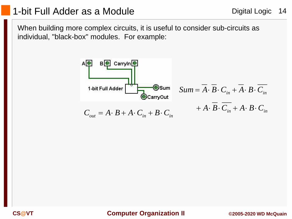
1-bit Full Adder as a Module
When building more complex circuits, it is useful to consider sub-circuits as
individual, "black-box" modules. For example:
inin
inin
CBACBA
CBACBASum
out in inC A B A C B C

Digital Logic
Computer Organization II
15
CS@VT ©2005-2020 WD McQuain
Chaining a 4-bit Adder
An 4-bit adder built by
chaining 1-bit adders:
This has one serious shortcoming. The carry bits must
ripple from top to bottom, creating a lag before the
result will be obtained for the final sum bit and carry.

Digital Logic
Computer Organization II
16
CS@VT ©2005-2020 WD McQuain
Carry-Lookahead Adder
Perhaps surprisingly, it's possible to compute all the carry bits before any sum bits
are computed... and that leads to a faster adder design:
Why is this faster than the ripple-carry approach?

Digital Logic
Computer Organization II
17
CS@VT ©2005-2020 WD McQuain
Latency
The answer lies in the concept of gate latency.
Each logic gate takes a certain amount of time (usually measured in picoseconds)
to stabilize on the correct output... we call that the latency of the gate.
For simplicity, we'll assume in this course that all gates (except inverters) have the
same latency, and that inverters are so fast they can be igored.
Then, the idea is that the latency of a circuit can be measured by the maximum
number of gates a signal passes through within the circuit... called the depth of the
circuit.
So, the 1-bit full adder we saw earlier has a depth of 2.
Digital Logic
Computer Organization II
18
CS@VT ©2005-2020 WD McQuain
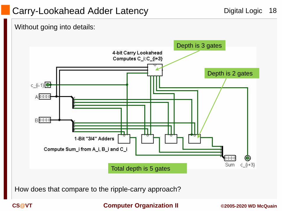
Carry-Lookahead Adder Latency
Without going into details:
How does that compare to the ripple-carry approach?
Depth is 3 gates
Depth is 2 gates
Total depth is 5 gates

Digital Logic
Computer Organization II
19
CS@VT ©2005-2020 WD McQuain
Ripple-carry Latency
A 4-bit ripple-carry design would have 4 1-bit full adders, and we've seen that each
of those has a depth of 2 gates.
But those adders fire sequentially, so running one after the other would entail a
total depth of 8 gates.
So, the ripple-carry design would be 1.6 times as "deep" and it's not unreasonable
to say it would take about 1.6 times as long to compute the result.
Just how you'd implement the computation of those carry bits is an interesting
question...

Digital Logic
Computer Organization II
20
CS@VT ©2005-2020 WD McQuain
Refined Adder Design
The following slides illustrate an approach used to improve efficiency, versus the
ripple-carry design covered earlier.
These may or not be covered, at the discretion of your instructor.

Digital Logic
Computer Organization II
21
CS@VT ©2005-2020 WD McQuain
Carry-Lookahead Logic
Let's look at just how the carry bits depend on the summand bits:
c4 c3 c2 c1 c0
a3 a2 a1 a0
b3 b2 b1 b0
-------------
s3 s2 s1 s0
It's clear that c1 = 1 if and only if at least two of the bits in the previous column
are 1.
Since this relationship holds for every carry bit (except c0), we have the following
general Boolean equation for carry bits:
We will allow for a carry-in in
the low-order position (c0).
1i i i i i i ic a b a c b c
(Note that • represents AND and + represents OR.)

Digital Logic
Computer Organization II
22
CS@VT ©2005-2020 WD McQuain
Now, this relationship doesn't seem to help until we look at it a bit more deeply:
1 ( )i i i i i i i i i i i ic a b a c b c a b a b c
Carry-Lookahead Logic
i i i
i i i
g a b
p a b
1 0 0 0
2 1 1 1 1 1 0 0 0 1 1 0 1 0 0( )
c g p c
c g p c g p g p c g p g p p c
If we define
then we get the following relationships:
Now, we can calculate all of the gi and pi terms at once, from the bits of the two
summands, and c0 will be given, so we can compute c1 and c2 before we actually
do the addition!

Digital Logic
Computer Organization II
23
CS@VT ©2005-2020 WD McQuain
Finally, here's how we can calculate c3 and c4:
Carry-Lookahead Logic
3 2 2 2
2 2 1 1 0 1 0 0
2 2 1 2 1 0 2 1 0 0
( )
c g p c
g p g p g p p c
g p g p p g p p p c
So, we have the necessary logic to implement the 4-bit Carry Lookahead unit for
our 4-bit Carry Lookahead Adder:
4 3 3 3
3 3 2 2 1 2 1 0 2 1 0 0
3 3 2 3 2 1 3 2 1 0 3 2 1 0 0
( )
c g p c
g p g p g p p g p p p c
g p g p p g p p p g p p p p c

Digital Logic
Computer Organization II
24
CS@VT ©2005-2020 WD McQuain
Carry-Lookahead Logic
i i i
i i i
g a b
p a b
1 0 0 0
2 1 1 0 1 0 0
3 2 2 1 2 1 0 2 1 0 0
4 3 3 2 3 2 1 3 2 1 0 3 2 1 0 0
c g p c
c g p g p p c
c g p g p p g p p p c
c g p g p p g p p p g p p p p c

Digital Logic
Computer Organization II
25
CS@VT ©2005-2020 WD McQuain
Abstraction
The gi and pi bits represent an abstract view of how carry bits are generated and
propagate during addition:
i i ig a b
i i ip a b
generate bit for i-th column
adding the summand bits generates a carry-
out bit iff both summand bits are 1
propagate bit for i-th column
if ci = 1 (the carry-out bit from the previous
column), there's a carry-out into the next
column iff at least one of the summand bits is 1

Digital Logic
Computer Organization II
26
CS@VT ©2005-2020 WD McQuain
Abstraction
So, here's why the formulas we've derived make sense intuitively:
1 0 0 0c g p c
4 3 3 2 3 2 1 3 2 1 0 3 2 1 0 0c g p g p p g p p p g p p p p c
c1 is 1 iff:
c0 was 1 and column 0 propagated it
or
column 0 generated a carry-out
c4 is 1 iff:
c0 was 1 and columns 0 to 3 propagated it, or
column 0 generated a carry-out and columns 1 to 3
propagated it, or
column 1 generated a carry-out and columns 2 to 3
propagated it, or
column 2 generated a carry-out and column 3
propagated it, or
column 3 generated a carry-out

Digital Logic
Computer Organization II
27
CS@VT ©2005-2020 WD McQuain
Implementation Below the Gate Level
The following slides illustrate how transistors might be used to implement the
logic gates introduced earlier.
These may or not be covered, at the discretion of your instructor.

Digital Logic
Computer Organization II
28
CS@VT ©2005-2020 WD McQuain
Aside: Transistors
Transistors are a primary building block for electronic circuits.
* By Brews ohare - Own work, CC BY-SA 3.0,
https://commons.wikimedia.org/w/index.php?curid=18796795
MOS-FET
(metal-oxide-semiconductor field-effect transistor)
Mohamed Atalla & Dawon Kahng, Bell Labs
gate input
source drain
base
insulator
1953 1959

Digital Logic
Computer Organization II
29
CS@VT ©2005-2020 WD McQuain
Aside: Transistors
gate input
source drain
base
insulator
P-type transistor
gate input 0: source is sent to drain
gate input 1: drain is "floating"
N-type transistor
gate input 0: drain is "floating"
gate input 1: source is sent to drain

Digital Logic
Computer Organization II
30
CS@VT ©2005-2020 WD McQuain
Aside: Implementing Logic Gates
Here's one way an inverter might be implemented:
(Apologies to electronics engineers for the inherent imprecision of this.)
data inputsource
Output signal equals complement of data input.
P-type transistor
gate input 0: source is sent to drain
gate input 1: drain is "floating"
drain
Pull resistor
(reduces signal that's less than 1 to 0)
gate

Digital Logic
Computer Organization II
31
CS@VT ©2005-2020 WD McQuain
Aside: Implementing Logic Gates
Here's one way an AND gate might be implemented:
(Apologies to electronics engineers for the inherent imprecision of this.)
data inputsource
Output signal equals AND of data inputs
N-type transistor
gate input 0: drain is "floating"
gate input 1: source is sent to drain
drain
Pull resistors
data input
gate

Digital Logic
Computer Organization II
32
CS@VT ©2005-2020 WD McQuain
Aside: Implementing Logic Gates
Here's one way an OR gate might be implemented:
(Apologies to electronics engineers for the inherent imprecision of this.)
data input source
Output signal equals OR of data inputs
N-type transistor
gate input 0: drain is "floating"
gate input 1: source is sent to drain
drain
Pull resistor
ga
te
data input