LNK623-626 LinkSwitch-CV Family - Power Integrations · Output Power Table Product3 230 VAC ±15%...
18
LNK623-626 LinkSwitch-CV Family www.power.com August 2015 Energy-Efficient, Off-line Switcher with Accurate Primary-side Constant-Voltage (CV) Control This Product is Covered by Patents and/or Pending Patent Applications. Output Power Table Product 3 230 VAC ±15% 85-265 VAC Adapter 1 Peak or Open Frame 2 Adapter 1 Peak or Open Frame 2 LNK623PG/DG 6.5 W 9 W 5.0 W 6 W LNK624PG/DG 7 W 11 W 5.5 W 6.5 W LNK625PG/DG 8 W 13.5 W 6.5 W 8 W LNK626PG/DG 10.5 W 17 W 8.5 W 10 W Table 1. Output Power Table. Based on 5 V Output. Notes: 1. Minimum continuous power in a typical non-ventilated enclosed adapter measured at +50 °C ambient. 2. Maximum practical continuous power in an open frame design with adequate heat sinking, measured at 50 °C ambient (see Key Application Considerations section for more information). 3. Packages: P: DIP-8C, D: SO-8C. Product Highlights Dramatically Simplifies CV Converters • Eliminates optocoupler and all secondary CV control circuitry • Eliminates bias winding supply – IC is self biasing Advanced Performance Features • Compensates for external component temperature variations • Very tight IC parameter tolerances using proprietary trimming technology • Continuous and/or discontinuous mode operation for design flexibility • Frequency jittering greatly reduces EMI filter cost • Even tighter output tolerances achievable with external resistor selection/trimming Advanced Protection/Safety Features • Auto-restart protection reduces delivered power by >95% for output short-circuit and all control loop faults (open and shorted components) • Hysteretic thermal shutdown – automatic recovery reduces power supply returns from the field • Meets HV creepage requirements between Drain and all other pins, both on the PCB and at the package EcoSmart™– Energy Efficient • No-load consumption <200 mW at 230 VAC and down to below 70 mW with optional external bias • Easily meets all global energy efficiency regulations with no added components • ON/OFF control provides constant efficiency down to very light loads – ideal for mandatory EISA and ENERGY STAR 2.0 regulations • No primary or secondary current sense resistors – maximizes efficiency Green Package • Halogen free and RoHS compliant package Applications • DVD/STB • Adapters • Standby and auxiliary supplies • Home appliances, white goods and consumer electronics • Industrial controls Description The LinkSwitch TM -CV dramatically simplifies low power, constant voltage (CV) converter design through a revolutionary control technique which eliminates the need for both an optocoupler and secondary CV control circuitry while providing very tight output voltage regulation. The combination of proprietary IC trimming and E-Shield™ transformer construction techniques enables Clampless™ designs with the LinkSwitch-CV LNK623/4. LinkSwitch-CV provides excellent cross-regulation for multiple-output flyback applications such as DVDs and STBs. A 725 V power MOSFET and ON/OFF control state machine, self-biasing, frequency jittering, cycle-by-cycle current limit, and hysteretic thermal shutdown circuitry are all incorporated onto one IC. Figure 1. Typical Application Schematic (a) and Output Characteristic Envelope (b). *Optional with LNK623-624PG/DG. (see Key Application Consider- ations section for clamp and other external circuit design considerations). LinkSwitch-CV * Wide Range High-Voltage DC Input PI-5195-012915 D S FB BP (a) Typical Application Schematic (b) Output Characteristic I O V O ±5% Auto-Restart PI-5196-012315 Figure 2. DIP-8C P and SO-8C D Packages.
Transcript of LNK623-626 LinkSwitch-CV Family - Power Integrations · Output Power Table Product3 230 VAC ±15%...

LNK623-626LinkSwitch-CV Family
www.power.com August 2015
Energy-Efficient, Off-line Switcher with Accurate Primary-side Constant-Voltage (CV) Control
This Product is Covered by Patents and/or Pending Patent Applications.
Output Power Table
Product3
230 VAC ±15% 85-265 VAC
Adapter1Peak or Open
Frame2Adapter1
Peak or Open
Frame2
LNK623PG/DG 6.5 W 9 W 5.0 W 6 W
LNK624PG/DG 7 W 11 W 5.5 W 6.5 W
LNK625PG/DG 8 W 13.5 W 6.5 W 8 W
LNK626PG/DG 10.5 W 17 W 8.5 W 10 W
Table 1. Output Power Table. Based on 5 V Output. Notes: 1. Minimum continuous power in a typical non-ventilated enclosed adapter
measured at +50 °C ambient. 2. Maximum practical continuous power in an open frame design with adequate
heat sinking, measured at 50 °C ambient (see Key Application Considerations section for more information).
3. Packages: P: DIP-8C, D: SO-8C.
Product HighlightsDramatically Simplifies CV Converters• Eliminates optocoupler and all secondary CV control circuitry • Eliminates bias winding supply – IC is self biasing
Advanced Performance Features• Compensates for external component temperature variations• Very tight IC parameter tolerances using proprietary trimming
technology • Continuous and/or discontinuous mode operation for design
flexibility• Frequency jittering greatly reduces EMI filter cost• Even tighter output tolerances achievable with external resistor
selection/trimming
Advanced Protection/Safety Features• Auto-restart protection reduces delivered power by >95% for
output short-circuit and all control loop faults (open and shorted components)
• Hysteretic thermal shutdown – automatic recovery reduces power supply returns from the field
• Meets HV creepage requirements between Drain and all other pins, both on the PCB and at the package
EcoSmart™– Energy Efficient• No-load consumption <200 mW at 230 VAC and down to below
70 mW with optional external bias • Easily meets all global energy efficiency regulations with no added
components• ON/OFF control provides constant efficiency down to very light
loads – ideal for mandatory EISA and ENERGY STAR 2.0 regulations• No primary or secondary current sense resistors – maximizes
efficiency
Green Package• Halogen free and RoHS compliant package
Applications• DVD/STB• Adapters• Standby and auxiliary supplies• Home appliances, white goods and consumer electronics• Industrial controls
DescriptionThe LinkSwitchTM-CV dramatically simplifies low power, constant voltage (CV) converter design through a revolutionary control technique which eliminates the need for both an optocoupler and secondary CV control circuitry while providing very tight output voltage regulation. The combination of proprietary IC trimming and E-Shield™ transformer construction techniques enables Clampless™ designs with the LinkSwitch-CV LNK623/4.
LinkSwitch-CV provides excellent cross-regulation for multiple-output flyback applications such as DVDs and STBs. A 725 V power MOSFET and ON/OFF control state machine, self-biasing, frequency jittering, cycle-by-cycle current limit, and hysteretic thermal shutdown circuitry are all incorporated onto one IC.
Figure 1. Typical Application Schematic (a) and Output Characteristic Envelope (b). *Optional with LNK623-624PG/DG. (see Key Application Consider- ations section for clamp and other external circuit design considerations).
LinkSwitch-CV
*
Wide RangeHigh-Voltage
DC Input
PI-5195-012915
D
S
FB
BP
(a) Typical Application Schematic
(b) Output CharacteristicIO
VO ±5%
Auto-Restart
PI-5196-012315
Figure 2. DIP-8C P and SO-8C D Packages.

Rev. H 08/15
2
LNK623-626
www.power.com
Pin Functional DescriptionDRAIN (D) Pin:This pin is the power MOSFET drain connection. It provides internal operating current for both start-up and steady-state operation.
BYPASS (BP) Pin:This pin is the connection point for an external bypass capacitor for the internally generated 6 V supply.
FEEDBACK (FB) Pin:During normal operation, switching of the power MOSFET is controlled by this pin. This pin senses the AC voltage on the bias winding. This control input regulates the output voltage based on the flyback voltage of the bias winding.
SOURCE (S) Pin:This pin is internally connected to the output MOSFET source for high-voltage power and control circuit common returns.
Figure 3 Functional Block Diagram.
Figure 4. Pin Configuration.
PI-5197-012915
SOURCE(S)
LEADINGEDGE
BLANKING
+
-
+
-+
-
DRAIN(D)
BYPASS(BP)
FEEDBACK(FB)
SOURCE(S)
FBOUT Reset
6 V5 V
tSAMPLE-OUT
VILIMITILIM
VTH VILIMIT
6.5 V
DriveILIM
DCMAX
tSAMPLE-OUT
DCMAX
FB
Current LimitComparator
STATEMACHINE
SAMPLEDELAY
THERMALSHUTDOWN
OSCILLATOR
FAULTAuto-RestartOpen-Loop
D Q
REGULATOR6 V
PI-5198-012315
D S
BP S
SFB
P Package (DIP-8C) D Package (SO-8C)
8
5
7
1
4
2
S6
FB
BP
D
1
2
4
8
7
6
5
S
S
S
S

Rev. H 08/15
3
LNK623-626
www.power.com
LinkSwitch-CV Functional DescriptionThe LinkSwitch-CV combines a high-voltage power MOSFET switch with a power supply controller in one device. Similar to the LinkSwitch-LP and TinySwitch-III it uses ON/OFF control to regulate the output voltage. The LinkSwitch-CV controller consists of an oscillator, feedback (sense and logic) circuit, 6 V regulator, over-temperature protection, frequency jittering, current limit circuit, leading-edge blanking, and ON/OFF state machine for CV control.
Constant Voltage (CV) OperationThe controller regulates the FEEDBACK pin voltage to remain at VFBth using an ON/OFF state-machine. The FEEDBACK pin voltage is sampled 2.5 ms after the turn-off of the high-voltage switch. At light loads the current limit is also reduced to decrease the transformer flux density.
Auto-Restart and Open-Loop ProtectionIn the event of a fault condition such as an output short or an open loop condition the LinkSwitch-CV enters into an appropriate protection mode as described below.
In the event the FEEDBACK pin voltage during the Flyback period falls below VFBth-0.3 V before the FEEDBACK pin sampling delay (~2.5 ms) for a duration in excess of 200 ms (auto-restart on-time (tAR-ON) the converter enters into auto-restart, wherein the power MOSFET is disabled for 2.5 seconds (~8% auto-restart duty cycle). The auto-restart alternately enables and disables the switching of the power MOSFET until the fault condition is removed.
In addition to the conditions for auto-restart described above, if the sensed FEEDBACK pin current during the Forward period of the conduction cycle (switch “on” time) falls below 120 mA, the converter annunciates this as an open-loop condition (top resistor in potential
divider is open or missing) and reduces the auto-restart time from 200 ms to approximately 6 clock cycles (90 ms), whilst keeping the disable period of 2.5 seconds. This effectively reduces the auto-restart duty cycle to less than 0.01%.
Over-Temperature ProtectionThe thermal shutdown circuitry senses the die temperature. The threshold is set at 142 °C typical with a 60 °C hysteresis. When the die temperature rises above this threshold (142 °C) the power MOSFET is disabled and remains disabled until the die temperature falls by 60 °C, at which point the MOSFET is re-enabled.
Current LimitThe current limit circuit senses the current in the power MOSFET. When this current exceeds the internal threshold (ILIMIT), the power MOSFET is turned off for the remainder of that cycle. The leading edge blanking circuit inhibits the current limit comparator for a short time (tLEB) after the power MOSFET is turned on. This leading edge blanking time has been set so that current spikes caused by capacitance and rectifier reverse recovery time will not cause premature termination of the MOSFET conduction.
6.0 V RegulatorThe 6 V regulator charges the bypass capacitor connected to the BYPASS pin to 6 V by drawing a current from the voltage on the DRAIN, whenever the MOSFET is off. The BYPASS pin is the internal supply voltage node. When the MOSFET is on, the device runs off of the energy stored in the bypass capacitor. Extremely low power consumption of the internal circuitry allows the LinkSwitch-CV to operate continuously from the current drawn from the DRAIN pin. A bypass capacitor value of 1 mF is sufficient for both high frequency decoupling and energy storage.

Rev. H 08/15
4
LNK623-626
www.power.com
Applications Example
Circuit DescriptionThis circuit is configured as a three output, primary-side regulated flyback power supply utilizing the LNK626PG. It can deliver 7 W continuously and 10 W peak (thermally limited) from an universal input voltage range (85 – 265 VAC). Efficiency is >67% at 115 VAC/230 VAC and no-load input power is <140 mW at 230 VAC.
Input FilterAC input power is rectified by diodes D1 through D4. The rectified DC is filtered by the bulk storage capacitors C1 and C2. Inductor L1, L2, C1 and C2 form a pi (π) filter, which attenuates conducted differential-mode EMI noise. This configuration along with Power Integrations transformer E-shield technology allow this design to meet EMI standard EN55022 class B with good margin without requiring a Y capacitor. Fuse F1 provides protection against catastrophic failure. Negative temperature coefficient thermistor RT1 limits the inrush current when AC is first applied to below the maximum rating of diodes D1 through D4. Metal oxide varistor RV1 clamps the AC input during differential line transients, protecting the input components and maintaining the peak drain voltage of U1 below its 725 V BVDSS rating. For differential surge levels at or below 2 kV this component may be omitted.
LNK626 PrimaryThe LNK626PG device (U1) incorporates the power switching device, oscillator, CV control engine, startup, and protection functions. The integrated 725 V MOSFET provides a large drain voltage margin in universal input AC applications, increasing reliability and also reducing the output diode voltage stress by allowing a greater transformer turns ratio. The device can be completely self-powered from the BYPASS pin and decoupling capacitor C4. In this design a bias circuit (D6, C6 and R4) was added to reduce no load input power below 140 mW.
The rectified and filtered input voltage is applied to one side of the primary winding of T1. The other side of the transformer’s primary winding is driven by the integrated MOSFET in U1. The leakage inductance drain voltage spike is limited by the clamp circuit D5, R1, R2, C3 and VR1. The Zener bleed clamp arrangement was selected for lowest no-load input power but in applications where higher no-load input power is acceptable VR1 may be omitted and the value of R1 increased to form a standard RCD clamp.
Output RectificationThe secondaries of the transformer are rectified by D7, D8 and D9. A Schottky barrier type was used for the main 5 V output for higher efficiency. The +12 V and -22 V outputs use an ultrafast rectifier diode. The main output is post filtered by L3 and C10 to remove switching frequency ripple. Resistors R7, R8 and R9 provide a preload to maintain the output voltages within their respective limits when unloaded. To reduce high frequency ringing and associated radiated EMI an RC snubber formed by R10 and C13 was added across D7.
Output RegulationThe LNK626 regulates the output using ON/OFF control, enabling or disabling switching cycles based on the sampled voltage on the FEEDBACK pin. The output voltage is sensed using a primary referenced winding on transformer T1 eliminating the need for an optocoupler and a secondary sense circuit. The resistor divider formed by R3 and R6 feeds the winding voltage into U1. Standard 1% resistor values were used to center the nominal output voltages. Resistor R5 and C5 reduce pulse grouping by creating an offset voltage that is proportional to the number of consecutive enabled switching cycles.
Figure 5. 7 W (10 W peak) Multiple Output Flyback Converter for DVD Applications with Primary Sensed Feedback.
PI-5205-012315
D
S
FB
BP
R36.34 kΩ
1%
C13270 pF
R64.02 kΩ
1%
R15.1 kΩ1/8 W
R2390 Ω
R46.2 kΩ
C41 µF50 V C5
680 pF50 V
C81000 µF
10 V
C10470 µF10 V
C1147 µF50 V
C947 µF25 V
C610 µF50 V
R547 kΩ1/8 W
U1LNK626PG
LinkSwitch-CV
D8UF4003
D7 SB540
D61N4148
D9UF4003
R939 kΩ1/8 W
R824 kΩ1/8 W
R7510 Ω1/8 W
T1EEL19
1 6
7
11
8,9,10
12
5
4
2
3
C122 µF400 V
C222 µF400 V
C3820 pF1 kV
F13.15 A
RT110 Ω
85 - 265VAC
L
N
D1FR106
D2FR106
VR11N5272B
D51N4007
D31N4007
D41N4007
L13.5 × 7.6 mmFerrite Bead
L2680 µH
L310 µH
12 V, 0.1 A
5 V, 1.7 A
RTN
-22 V, 15 mARV1275 V
R1047 Ω

Rev. H 08/15
5
LNK623-626
www.power.com
Key Application ConsiderationsOutput Power TableThe data sheet maximum output power table (Table 1) represents the maximum practical continuous output power level that can be obtained in a Flyback converter under the following assumed conditions:
1. The minimum DC input voltage is 100 V or higher at 90 VAC input. The value of the input capacitance should be large enough to meet these criteria for AC input designs.
2. Secondary output of 5 V with a Schottky rectifier diode.3. Assumed efficiency of 80%.4. Continuous conduction mode operation (KP = 0.4).5. Reflected Output Voltage (VOR) of 110 V.6. The part is board mounted with SOURCE pins soldered to a
sufficient area of copper to keep the SOURCE pin temperature at or below 110 °C for P package and 100 °C for D packaged devices.
7. Ambient temperature of 50 °C for open frame designs and an internal enclosure temperature of 60 °C for adapter designs.
Note: Higher output power are achievable if the efficiency is higher than 80%, typically for high output voltage designs.
BYPASS Pin Capacitor A 1 mF BYPASS pin capacitor (C4) is recommended. The capacitor voltage rating should be equal to or greater than 6.8 V. The capacitor’s dielectric material is not important. The capacitor must be physically located close to the LinkSwitch-CV BYPASS pin.
Circuit board layoutLinkSwitch-CV is a highly integrated power supply solution that integrates on a single die, both the controller and the high-voltage MOSFET. The presence of high switching currents and voltages together with analog signals makes it especially important to follow good PCB design practice to ensure stable and trouble free operation of the power supply.
When designing a board for the LinkSwitch-CV based power supply, it is important to follow the following guidelines:
Single Point GroundingUse a single point (Kelvin) connection at the negative terminal of the input filter capacitor for the LinkSwitch-CV SOURCE pin and bias winding return. This improves surge capabilities by returning surge currents from the bias winding directly to the input filter capacitor.
Bypass CapacitorThe BYPASS pin capacitor should be located as close as possible to the SOURCE and BYPASS pins.
Feedback ResistorsPlace the feedback resistors directly at the FEEDBACK pin of the LinkSwitch-CV device. This minimizes noise coupling.
Thermal ConsiderationsThe copper area connected to the SOURCE pins provide the LinkSwitch-CV heat sink. A rule of thumb estimate is that the LinkSwitch-CV will dissipate 10% of the output power. Provide enough copper area to keep the SOURCE pin temperature below 110° C to provide margin for part to part RDS(ON) variation.
Secondary Loop AreaTo minimize leakage inductance and EMI, the area of the loop connecting the secondary winding, the output diode and the output filter capacitor should be minimized. In addition, sufficient copper area should be provided at the anode and cathode terminal of the diode for heat sinking. A larger area is preferred at the quiet cathode terminal. A large anode area can increase high frequency radiated EMI.
Electrostatic Discharge Spark GapIn chargers and adapters ESD discharges may be applied to the output of the supply. In these applications the addition of a spark gap is recommended. A trace is placed along the isolation barrier to form one electrode of a spark gap. The other electrode, on the secondary side, is formed by the output return node. The arrange-ment directs ESD energy from the secondary to the primary side AC input. A 10 mil gap is placed near the AC input. The gap decouples any noise picked up on the spark gap trace to the AC input. The trace from the AC input to the spark gap electrode should be spaced away from other traces to prevent unwanted arcing occurring and possible circuit damage.

Rev. H 08/15
6
LNK623-626
www.power.com
Figure 6. PCB Layout Example.
Figure 7. Schematic Representation of Recommended Layout Without External Bias.
Figure 8. Schematic Representation of Recommended Layout With External Bias.
+ -ACIN
PI-5269-012315
Y1Capacitor(optional)
Isolation Barrier
Transformer
T1
OutputRectifiers
Primary Side Secondary Side
R1
JP1
J1
C1
R3
R4
C12
R10D9
C11
C13
D7
C9R9R8D8
1 6
R7
C8
L3
C10
C2
R2C3
D1 D3
D5
VR1
D6C6R6
R5C5
C4
D4
RV1F1
D2
RT1
L2
L1
J2
Input FilterCapacitor
Drain trace areaminiminzed
ClampComponents
Copper areamaximized forheat sinking
DC Outputs
ESDspark gap
BypassCapacitor
close to device
FeedbackResistors close
to device
10 milgap
U1S
FB
BP
DSSS
Output FilterCapacitor
PI-5265-012315Kelvin connection atSOURCE pin, no powercurrents in signal traces
Minimize FEEDBACKpin node
area
CLAMP
D
S
FB
BP
B+
PRI RTN
Bias currents return to bulk capacitor
PI-5266-012315Kelvin connection atSOURCE pin, no powercurrents in signal traces
Bias currents return to bulk capacitor
Small FEEDBACKpin node area
Bias resistor
CLAMP
D
S
FB
BP
PRI RTN
B+

Rev. H 08/15
7
LNK623-626
www.power.com
Figure 9. Schematic Representation of Electrical Impact of Improper Layout.
PI-5267-012615
Bias winding currents flow in
signal source traces
Voltage drops across trace impedance may cause degraded performance
Power currentsflow in signalsource trace
Line surgecurrents canflow throughdevice
Drain trace in closeproximity of feedback trace
will couple noise intofeedback signal
B+
PRI RTN
CLAMP
D
S
FB
BP
∆VS
IsourceTraceimpedance

Rev. H 08/15
8
LNK623-626
www.power.com
Drain ClampRecommended Clamp Circuits
Components R1, R2, C3, VR1 and D5 in Figure 5 comprise the clamp. This circuit is preferred when the primary leakage inductance is greater than 125 mH to reduce drain voltage overshoot or ringing present on the feedback winding. For best output regulation, the feedback voltage must settle to within 1% at 2.1 ms from the turn off of the primary MOSFET. This requires careful selection of the clamp circuit components. The voltage of VR1 is selected to be ~20% above the reflected output voltage (VOR). This is to clip any turn off spike on the drain but avoid conduction during the flyback voltage interval when the output diode is conducting. The value of R1 should be the largest value that results in acceptable settling of the FEEDBACK pin voltage and peak drain voltage. Making R1 too large will increase the discharge time of C3 and degrade regulation. Resistor R2 dampens the leakage inductance ring. The value must be large enough to dampen the ring in the required time but must not be too large to cause the drain voltage to exceed 680 V.
If the primary leakage inductance is less than 125 mH, VR1 can be eliminated and the value of R1 increased. A value of 470 kW with an 820 pF capacitor is a recommended starting point. Verify that the peak drain voltage is less than 680 V under all line and load conditions. Verify the feedback winding settles to an acceptable limit for good line and load regulation.
Effect of Fast (500 ns) versus Slow (2 ms) Recovery Diodes in Clamp Circuit on Pulse Grouping and Output Ripple.
A slow reverse recovery diode reduces the feedback voltage ringing. The amplitude of ringing with a fast diode represents 8% error in Figure 11.
Figure 10. RCD Clamp, Low Power or Low Leakage Inductance Designs. RCD Clamp With Zener Bleed. High Power or High Leakage Inductance Designs.
Figure 11. Effect of Clamp Diode on FEEDBACK Pin Settling. Clamp Circuit (top). FEEDBACK Pin Voltage (bottom).
CC1
RC1
RC2
DC1
PI-5107-012615
DC2
RC2
RC1
CC1
DC1
PI-5108-110308
CC1
RC1
RC2
DC1
PI-5107-012615
Black Trace: DC1 is a FR107 (fast type, trr = 500 ns)Gray Trace: DC1 is a 1N4007G (standard recovery, trr = 2 us)

Rev. H 08/15
9
LNK623-626
www.power.com
Figure 12. Not Pulse Grouping (<5 Consecutive Switching Cycles). Pulse Grouping (>5 Consecutive Switching Cycles).
Top Trace: Drain Waveform (200 V/div)Bottom Trace: Output Ripple Voltage (50 mV/div)
Split Screen with Bottom Screen ZoomTop Trace: Drain Waveform (200 V/div)Bottom Trace: Output Ripple Voltage (50 mV/div)
Clampless DesignsClampless designs rely solely on the drain node capacitance to limit the leakage inductance induced peak drain-to-source voltage. Therefore the maximum AC input line voltage, the value of VOR, the leakage inductance energy, (a function of leakage inductance and peak primary current), and the primary winding capacitance determine the peak drain voltage. With no significant dissipative element present, as is the case with an external clamp, the longer duration of the leakage inductance ringing can increase EMI.
The following requirements are recommended for a universal input or 230 VAC only Clampless design:
1. Clampless designs should only be used for PO ≤5 W using a VOR of ≤90 V
2. For designs with PO ≤5 W, a two-layer primary must be used to ensure adequate primary intra-winding capacitance in the range of 25 pF to 50 pF. A bias winding must be added to the trans-former using a standard recovery rectifier diode (1N4003– 1N4007) to act as a clamp. This bias winding may also be used to externally power the device by connecting a resistor from the bias winding capacitor to the BYPASS pin. This inhibits the internal high-voltage current source, reducing device dissipation and no-load consumption.
3. For designs with PO >5 W, Clampless designs are not practical and an external RCD or Zener clamp should be used.
4. Ensure that worst-case, high line, peak drain voltage is below the BVDSS specification of the internal MOSFET and ideally ≤650 V to allow margin for design variation.
VOR (Reflected Output Voltage), is the secondary output plus output diode forward voltage drop that is reflected to the primary via the turns ratio of the transformer during the diode conduction time. The VOR adds to the DC bus voltage and the leakage spike to determine the peak drain voltage.
Pulse GroupingPulse grouping is defined as 6 or more consecutive pulses followed by two or more timing state changes. The effect of pulse grouping is increased output voltage ripple. This is shown on the right of Figure 12 where pulse grouping has caused an increase in the output ripple.
To eliminate group pulsing verify that the feedback signal settles within 2.1 ms from the turn off of the internal MOSFET. A Zener diode in the clamp circuit may be needed to achieve the desired settling time. If the settling time is satisfactory, then a RC network across RLOWER (R6) of the feedback resistors is necessary.
The value of R (R5 in the Figure 13) should be an order of magnitude greater than RLOWER and selected such that R×C = 32 ms where C is C5 in Figure 13.
Quick Design ChecklistAs with any power supply design, all LinkSwitch-CV designs should be verified on the bench to make sure that component specifications are not exceeded under worst-case conditions. The following minimum set of tests is strongly recommended:
1. Maximum drain voltage – Verify that peak VDS does not exceed 680 V at highest input voltage and maximum output power.
Figure 13. RC Network Across RBOTTOM (R6) to Reduce Pulse Grouping.
PI-5268-110608
D
S
FB
BP
R36.34 kΩ
1%
R64.02 kΩ
1%
R46.2 kΩ
C41 µF50 V C5
680 pF50 V
C610 µF50 V
R547 kΩ1/8 W
U1LNK626PG
LinkSwitch-CV
D61N4148
5
4
2
Top Trace: Drain Waveform (200 V/div)Bottom Trace: Output Ripple Voltage (50 mV/div)
Split Screen with Bottom Screen ZoomTop Trace: Drain Waveform (200 V/div)Bottom Trace: Output Ripple Voltage (50 mV/div)

Rev. H 08/15
10
LNK623-626
www.power.com
2. Maximum drain current – At maximum ambient temperature, maximum input voltage and maximum output load, verify drain current waveforms at start-up for any signs of transformer saturation and excessive leading edge current spikes. LinkSwitch-CV has a leading edge blanking time of 215 ns to prevent premature termination of the ON-cycle. Verify that the leading edge current spike is below the allowed current limit envelope for the drain current waveform at the end of the 215 ns blanking period.
3. Thermal check – At maximum output power, both minimum and maximum input voltage and maximum ambient temperature; verify that temperature specifications are not exceeded for
LinkSwitch-CV, transformer, output diodes and output capacitors. Enough thermal margin should be allowed for the part-to-part variation of the RDS(ON) of LinkSwitch-CV, as specified in the data sheet. It is recommended that the maximum SOURCE pin temperature does not exceed 110 °C.
Design ToolsUp-to-date information on design tools can be found at the Power Integrations web site: www.power.com

Rev. H 08/15
11
LNK623-626
www.power.com
Parameter SymbolConditions
SOURCE = 0 V; TJ = -40 to 125 °C (Unless Otherwise Specified)
Min Typ Max Units
Control Functions
Output Frequency fOSC TJ = 25 °C, VFB = VFBth LNK623/6 93 100 106 kHz
Frequency Jitter Peak-Peak Jitter Compared to Average Frequency, TJ = 25 °C ±7 %
Ratio of Output Frequency at Auto- Restart
fOSC(AR)
TJ = 25 °C Relative to fOSC , See Note C 80 %
Maximum Duty Cycle DCMAX
TJ = 25 °CSee Notes B, C 54 %
FEEDBACK Pin Voltage VFBth
TJ = 25 °C See Figure 15
CBP = 1 mFSee Note D
LNK623-624P 1.815 1.840 1.865
VLNK623-624D 1.855 1.880 1.905
LNK625P, LNK625D 1.835 1.860 1.885
LNK626P, LNK626D 1.775 1.800 1.825
FEEDBACK Pin Voltage Temperature Coefficient
TCVFB -0.01 %/°C
FEEDBACK Pin Voltage at Turn-Off Threshold VFB(AR) 1.45 V
Power Coefficient I2f
I2f = I2LIMIT(TYP) × fOSC(TYP)
LNK623/6PTJ = 25 °C 0.9 × I2f I2f 1.17 × I2f
A2Hz
I2f = I2LIMIT(TYP) × fOSC(TYP)
LNK623/6DTJ = 25 °C 0.9 × I2f I2f 1.21 × I2f
Absolute Maximum Ratings1,5
DRAIN Voltage ........................................................-0.3 V to 725 VDRAIN Peak Current: LNK623 .................................400 (600) mA4
LNK624 .................................400 (600) mA4
LNK625 .................................528 (790) mA4
LNK626 ............................... 720 (1080) mA4
Peak Negative Pulsed DRAIN Current .................................-100 mA2 Feedback Pin Voltage .................................................. -0.3 V to 9 V Feedback Pin Current ..........................................................100 mABYPASS Pin Voltage .................................................... -0.3 V to 9 VBYPASS Pin Current ...............................................................10 mA Storage Temperature ...................................... ..........-65 °C to 150 °COperating Junction Temperature ..............................-40 °C to 150 °C Lead Temperature(3) .............................................................. 260 °C
Notes: 1. All voltages referenced to SOURCE, TA = 25 °C. 2. Duration not to exceed 2 msec. 3. 1/16 in. from case for 5 seconds.4. The higher peak DRAIN current is allowed while the DRAIN voltage is simultaneously less than 400 V. 5. Maximum ratings specified may be applied, one at a time without causing permanent damage to the product. Exposure to Absolute Maximum ratings for extended periods of time may affect product reliability.
Thermal Resistance
Thermal Resistance: P Package: (qJA) .......................... .............. 70 °C/W2; 60 °C/W3
(qJC)1 ...................................................... 11 °C/W
D Package: (qJA) .....................................100 °C/W2; 80 °C/W3
(qJC)1 ....................................................... 30 °C/W
Notes: 1. Measured on pin 8 (SOURCE) close to plastic interface. 2. Soldered to 0.36 sq. in. (232 mm2), 2 oz. (610 g/m2) copper clad. 3. Soldered to 1 sq. in. (645 mm2), 2 oz. (610 g/m2) copper clad.

Rev. H 08/15
12
LNK623-626
www.power.com
Parameter SymbolConditions
SOURCE = 0 V; TJ = -40 to 125 °C (Unless Otherwise Specified)
Min Typ Max Units
Control Functions (cont.)
Minimum Switch “On”-Time tON(min) See Note C 700 ns
FEEDBACK Pin Sampling Delay tFB 2.35 2.55 2.75 ms
DRAIN Supply Current
IS1 FB Voltage > VFBth 280 330
mAIS2
FB Voltage = VFBth -0.1, Switch ON-Time = tON (MOSFET
Switching at fOSC)
LNK623/4 440 520
LNK625 480 560
LNK626 520 600
BYPASS Pin Charge Current
ICH1 VBP = 0 V LNK623/4 -5.0 -3.4 -1.8
mALNK625/6 -7.0 -4.5 -2.0
ICH2 VBP = 4 VLNK623/4 -4.0 -2.3 -1.0
LNK625/6 -5.6 -3.2 -1.4
BYPASS Pin Voltage VBP 5.65 6.00 6.25 V
BYPASS Pin Voltage Hysteresis VBPH 0.70 1.00 1.20 V
BYPASS Pin Shunt Voltage VSHUNT 6.2 6.5 6.8 V
Circuit Protection
Current Limit ILIMIT
LNK623 di/dt = 50 mA/ms , TJ = 25 °C 196 210 225
mA
LNK624 di/dt = 60 mA/ms , TJ = 25 °C 233 250 268
LNK625di/dt = 80 mA/ms , TJ = 25 °C 307 330 353
LNK626 di/dt = 110 mA/ms , TJ = 25 °C 419 450 482
Leading Edge Blanking Time tLEB
TJ = 25 °C See Note C 170 215 ns
Thermal Shutdown Temperature TSD 135 142 150 °C
Thermal Shutdown Hysteresis TSDH 60 °C
Rev. H 08/15
13
LNK623-626
www.power.com
Parameter SymbolConditions
SOURCE = 0 V; TJ = -40 to 125 °C (Unless Otherwise Specified)
Min Typ Max Units
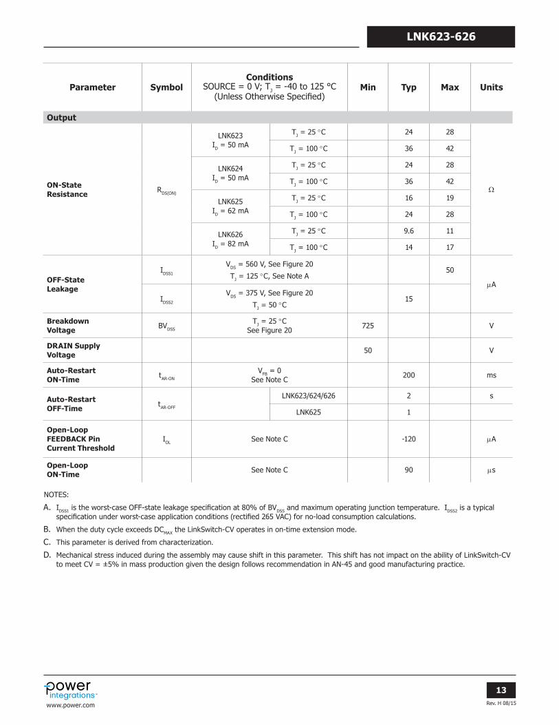
Output
ON-State Resistance RDS(ON)
LNK623ID = 50 mA
TJ = 25 °C 24 28
W
TJ = 100 °C 36 42
LNK624ID = 50 mA
TJ = 25 °C 24 28
TJ = 100 °C 36 42
LNK625ID = 62 mA
TJ = 25 °C 16 19
TJ = 100 °C 24 28
LNK626ID = 82 mA
TJ = 25 °C 9.6 11
TJ = 100 °C 14 17
OFF-State Leakage
IDSS1
VDS = 560 V, See Figure 20
TJ = 125 °C, See Note A50
mA
IDSS2
VDS = 375 V, See Figure 20
TJ = 50 °C15
Breakdown Voltage BVDSS
TJ = 25 °C See Figure 20 725 V
DRAIN Supply Voltage 50 V
Auto-Restart ON-Time tAR-ON
VFB = 0 See Note C 200 ms
Auto-Restart OFF-Time tAR-OFF
LNK623/624/626 2 s
LNK625 1
Open-Loop FEEDBACK Pin Current Threshold
IOL See Note C -120 mA
Open-Loop ON-Time See Note C 90 ms
NOTES:
A. IDSS1 is the worst-case OFF-state leakage specification at 80% of BVDSS and maximum operating junction temperature. IDSS2 is a typical specification under worst-case application conditions (rectified 265 VAC) for no-load consumption calculations.
B. When the duty cycle exceeds DCMAX the LinkSwitch-CV operates in on-time extension mode.
C. This parameter is derived from characterization.
D. Mechanical stress induced during the assembly may cause shift in this parameter. This shift has not impact on the ability of LinkSwitch-CV to meet CV = ±5% in mass production given the design follows recommendation in AN-45 and good manufacturing practice.

Rev. H 08/15
14
LNK623-626
www.power.com
1.200
0.600
0.800
1.000
0.200
0.400
0.000-40 -15 10 35 60 85 110 135
Temperature (°C)
Freq
uen
cy(N
orm
aliz
ed t
o 2
5 °
C)
PI-
50
86
-01
23
15 1.200
0.600
0.800
1.000
0.200
0.400
0.000-40 -15 10 35 60 85 110 135
Temperature (°C)
Feed
back
Vol
tage
(Nor
mal
ized
to
25
°C
)
PI-
50
89
-01
23
15
Figure 14. Output Frequency vs. Temperature. Figure 15. Feedback Voltage vs. Temperature.
Typical Performance Characteristics
Figure 16. Breakdown vs. Temperature.
1.1
1.0
0.9-50 -25 0 25 50 75 100 125 150
Junction Temperature (°C)
Bre
akdo
wn
Vol
tage
(Nor
mal
ized
to
25
°C
)
PI-
22
13
-01
23
15
DRAIN Voltage (V)
Dra
in C
urr
ent
(mA
)
300
250
200
100
50
150
00 2 4 6 8 10
TCASE=25 °CTCASE=100 °C
PI-
52
11
-08
07
08
LNK623 1.0LNK624 1.0LNK625 1.5LNK626 2.5
Scaling Factors:
Drain Voltage (V)
Dra
in C
apac
itan
ce (
pF)
PI-
52
01
-01
26
15
0 100 200 300 400 500 6001
10
100
1000
LNK623 1.0LNK624 1.0LNK625 1.5LNK626 2.5
Scaling Factors:50
30
40
10
20
00 200 400 600
DRAIN Voltage (V)
Pow
er (
mW
)
PI-
52
12
-01
26
15
LNK623 1.0LNK624 1.0LNK625 1.5LNK626 2.5
Scaling Factors:
Figure 17. Output Characteristic.
Figure 18. COSS vs. Drain Voltage. Figure 19. Drain Capacitance Power.

Rev. H 08/15
15
LNK623-626
www.power.com
Figure 20. Test Set-up for Leakage and Breakdown Tests.
PI-5203-012615
16 V
To measure BVDSS, IDSS1, and IDSS2 follow these steps:1) Close S1, open S22) Power-up VIN source (16 V)3) Open S1, close S24) Measure I/V characteristics of DRAIN pin using the curve tracer
S
D S
S
FB
S
.1 µF
1 µF BP
VIN
LinkSwitch-CV
5 µF 50 kΩ
+
CurveTracer
S1 S24 kΩ
10 kΩ

Rev. H 08/15
16
LNK623-626
www.power.com
Notes:1. Package dimensions conform to JEDEC specification MS-001-AB (Issue B 7/85) for standard dual-in-line (DIP) package with .300 inch row spacing.2. Controlling dimensions are inches. Millimeter sizes are shown in parentheses.3. Dimensions shown do not include mold flash or other protrusions. Mold flash or protrusions shall not exceed .006 (.15) on any side.4. Pin locations start with Pin 1, and continue counter-clock- wise to Pin 8 when viewed from the top. The notch and/or dimple are aids in locating Pin 1. Pin 3 is omitted.5. Minimum metal to metal spacing at the package body for the omitted lead location is .137 inch (3.48 mm).6. Lead width measured at package body. 7. Lead spacing measured with the leads constrained to be perpendicular to plane T.
.008 (.20)
.015 (.38)
.300 (7.62) BSC(NOTE 7)
.300 (7.62)
.390 (9.91)
.367 (9.32)
.387 (9.83)
.240 (6.10)
.260 (6.60)
.125 (3.18)
.145 (3.68)
.057 (1.45)
.068 (1.73)
.120 (3.05)
.140 (3.56)
.015 (.38)MINIMUM
.048 (1.22)
.053 (1.35).100 (2.54) BSC
.014 (.36)
.022 (.56)
-E-
Pin 1
SEATINGPLANE
-D-
-T-
P08C
PDIP-8C (P Package)
PI-3933-012315
D S .004 (.10)⊕
T E D S .010 (.25) M⊕
(NOTE 6)
.137 (3.48)MINIMUM
Rev. H 08/15
17
LNK623-626
www.power.com
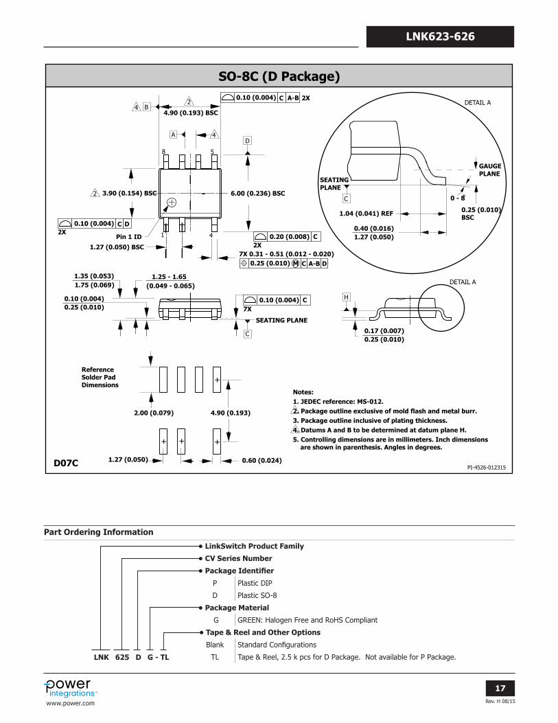
Part Ordering Information
• LinkSwitch Product Family
• CV Series Number
• Package Identifier
P Plastic DIP
D Plastic SO-8
• Package Material
G GREEN: Halogen Free and RoHS Compliant
• Tape & Reel and Other Options
Blank Standard Configurations
TL Tape & Reel, 2.5 k pcs for D Package. Not available for P Package.LNK 625 D G - TL
PI-4526-012315D07C
3.90 (0.154) BSC
Notes:1. JEDEC reference: MS-012.2. Package outline exclusive of mold flash and metal burr.3. Package outline inclusive of plating thickness.4. Datums A and B to be determined at datum plane H.5. Controlling dimensions are in millimeters. Inch dimensions are shown in parenthesis. Angles in degrees.
0.20 (0.008) C2X
1 4
58
2 6.00 (0.236) BSC
D4A
4.90 (0.193) BSC
2
0.10 (0.004) C2X
D
0.10 (0.004) C 2X A-B
1.27 (0.050) BSC7X 0.31 - 0.51 (0.012 - 0.020)
0.25 (0.010) M C A-B D
0.25 (0.010)0.10 (0.004)
(0.049 - 0.065)1.25 - 1.65
1.75 (0.069)1.35 (0.053)
0.10 (0.004) C7X
C
H
o
1.27 (0.050)0.40 (0.016)
GAUGEPLANE
0 - 8
1.04 (0.041) REF 0.25 (0.010)BSC
SEATINGPLANE
0.25 (0.010)0.17 (0.007)
DETAIL A
DETAIL A
C
SEATING PLANE
Pin 1 ID
B4
+
+ +
4.90 (0.193)
1.27 (0.050) 0.60 (0.024)
2.00 (0.079)
ReferenceSolder PadDimensions
+
SO-8C (D Package)
Revision Notes Date
B Release data sheet. 11/08C Correction made to Figure 5. 12/08D Introduced Max Current Limit when V DRAIN is below 400 V. 07/09E Introduced LNK626DG. 09/09F Added Note 4 to Parameter Table 02/10F Specified Max BYPASS Pin Current. 03/14
G Figure removed “Test Set-up for FEEDBACK Pin Measurements” from previous version. Updated tAR-OFF parameter. Updated to latest Brand Style. 02/15
H Update BVDSS from 700 V to 725 V 08/15
For the latest updates, visit our website: www.power.comPower Integrations reserves the right to make changes to its products at any time to improve reliability or manufacturability. Power Integrations does not assume any liability arising from the use of any device or circuit described herein. POWER INTEGRATIONS MAKES NO WARRANTY HEREIN AND SPECIFICALLY DISCLAIMS ALL WARRANTIES INCLUDING, WITHOUT LIMITATION, THE IMPLIED WARRANTIES OF MERCHANTABILITY, FITNESS FOR A PARTICULAR PURPOSE, AND NON-INFRINGEMENT OF THIRD PARTY RIGHTS.
Patent InformationThe products and applications illustrated herein (including transformer construction and circuits external to the products) may be covered by one or more U.S. and foreign patents, or potentially by pending U.S. and foreign patent applications assigned to Power Integrations. A complete list of Power Integrations patents may be found at www.power.com. Power Integrations grants its customers a license under certain patent rights as set forth at http://www.power.com/ip.htm.
Life Support PolicyPOWER INTEGRATIONS PRODUCTS ARE NOT AUTHORIZED FOR USE AS CRITICAL COMPONENTS IN LIFE SUPPORT DEVICES OR SYSTEMS WITHOUT THE EXPRESS WRITTEN APPROVAL OF THE PRESIDENT OF POWER INTEGRATIONS. As used herein:
1. A Life support device or system is one which, (i) is intended for surgical implant into the body, or (ii) supports or sustains life, and (iii) whose failure to perform, when properly used in accordance with instructions for use, can be reasonably expected to result in significant injury or death to the user.
2. A critical component is any component of a life support device or system whose failure to perform can be reasonably expected to cause the failure of the life support device or system, or to affect its safety or effectiveness.
The PI logo, TOPSwitch, TinySwitch, LinkSwitch, LYTSwitch, InnoSwitch, DPA-Switch, PeakSwitch, CAPZero, SENZero, LinkZero, HiperPFS, HiperTFS, HiperLCS, Qspeed, EcoSmart, Clampless, E-Shield, Filterfuse, FluxLink, StakFET, PI Expert and PI FACTS are trademarks of Power Integrations, Inc. Other trademarks are property of their respective companies. ©2015, Power Integrations, Inc.
World Headquarters5245 Hellyer AvenueSan Jose, CA 95138, USA.Main: +1-408-414-9200Customer Service:Phone: +1-408-414-9665Fax: +1-408-414-9765e-mail: [email protected]
China (Shanghai)Rm 2410, Charity Plaza, No. 88North Caoxi RoadShanghai, PRC 200030Phone: +86-21-6354-6323Fax: +86-21-6354-6325e-mail: [email protected]
China (Shenzhen)17/F, Hivac Building, No. 2, Keji Nan 8th Road, Nanshan District, Shenzhen, China, 518057Phone: +86-755-8672-8689Fax: +86-755-8672-8690e-mail: [email protected]
GermanyLindwurmstrasse 11480337 MunichGermanyPhone: +49-895-527-39110Fax: +49-895-527-39200e-mail: [email protected]
India#1, 14th Main RoadVasanthanagarBangalore-560052 IndiaPhone: +91-80-4113-8020Fax: +91-80-4113-8023e-mail: [email protected]
ItalyVia Milanese 20, 3rd. Fl.20099 Sesto San Giovanni (MI) ItalyPhone: +39-024-550-8701Fax: +39-028-928-6009e-mail: [email protected]
JapanKosei Dai-3 Bldg. 2-12-11, Shin-Yokohama, Kohoku-ku Yokohama-shi Kanagwan 222-0033 JapanPhone: +81-45-471-1021Fax: +81-45-471-3717e-mail: [email protected]
KoreaRM 602, 6FLKorea City Air Terminal B/D, 159-6Samsung-Dong, Kangnam-Gu,Seoul, 135-728, KoreaPhone: +82-2-2016-6610Fax: +82-2-2016-6630e-mail: [email protected]
Singapore51 Newton Road#19-01/05 Goldhill PlazaSingapore, 308900Phone: +65-6358-2160Fax: +65-6358-2015e-mail: [email protected]
Taiwan5F, No. 318, Nei Hu Rd., Sec. 1Nei Hu Dist.Taipei 11493, Taiwan R.O.C.Phone: +886-2-2659-4570Fax: +886-2-2659-4550e-mail: [email protected]
UKCambridge Semiconductor,a Power Integrations companyWestbrook Centre, Block 5, 2nd FloorMilton RoadCambridge CB4 1YGPhone: +44 (0) 1223-446483e-mail: [email protected]
Power Integrations Worldwide Sales Support Locations