LNA Linearization Using Bipolar...
18
1 LNA Linearization Using Bipolar Transistors Authors: Chunyu Xin and Edgar Sánchez-Sinencio Analog & Mixed Signal Center Electrical Engineering Department Texas A&M University
Transcript of LNA Linearization Using Bipolar...

1
LNA LinearizationUsing
Bipolar TransistorsAuthors: Chunyu Xin and Edgar Sánchez-Sinencio
Analog & Mixed Signal CenterElectrical Engineering Department
Texas A&M University
2
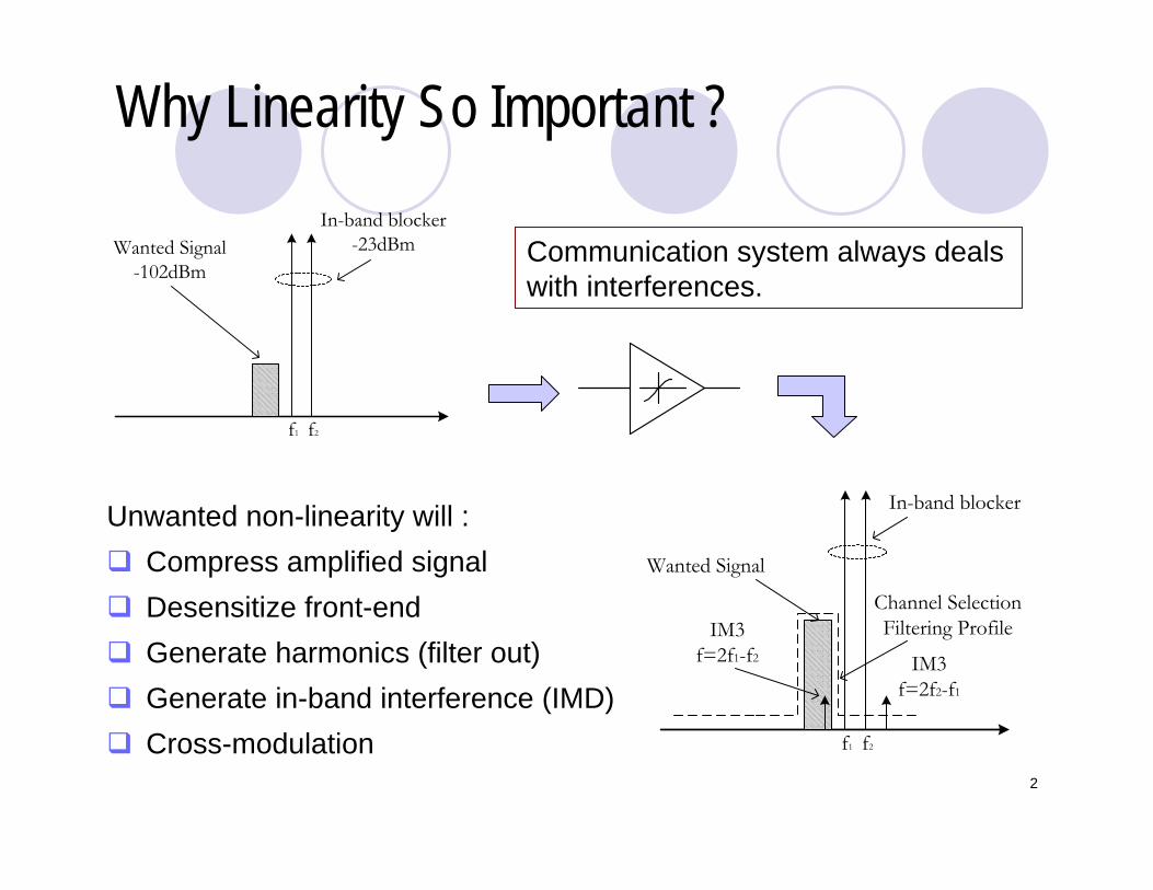
Why Linearity So Important ?
Unwanted non-linearity will :Compress amplified signalDesensitize front-endGenerate harmonics (filter out)Generate in-band interference (IMD)Cross-modulation
Communication system always deals with interferences.
Wanted Signal-102dBm
In-band blocker-23dBm
f1 f2
Wanted Signal
IM3f=2f1-f2
In-band blocker
f1 f2
Channel SelectionFiltering Profile
IM3f=2f2-f1

3
Linearity Metrics
P1dB@input
P1dB@output1dB
Pout (dB)
Pin (dB)
1dB compression: Measure gain compression for large input signal
IIP3/IIP2: Measure inter-modulation behavior
Relationships between IIP3 and P1dBFor one tone test: IIP3-P1dB=10dBFor two tone test: IIP3-P1dB=15dB
Fund
amen
tal
IM3 IM2
IIP2
OIP2
OIP3
IIP3
Pout(dBm)
Pin (dBm)

4
Non-linearity Terms of MOS Device
( ) 33
22 gsgsgsmgsds vgvgvgvi ++=
Intrinsic MOS I-V characteristic:
-0.22
-0.16
-0.10
-0.04
0.02
0.08
0.14
0.20
0.26
0.32
0.20 0.28 0.36 0.44 0.52 0.60 0.68 0.76 0.840.00
0.01
0.02
0.03
0.04
0.05
0.06
0.07
0.08
g 2(A/
V )
2g 3
(A/V
)3
g3
g2
gm
g m(A/
V)
Vth
Vgs(V)
mg 2g3g
( )( )21
2
od
odod
VVKV
θθ
++
( )31 odVKθ+ ( )41 odV
Kθθ+
−Strong/moderate
t
sIηφ
0
( )20
2 t
sIηφ ( )3
0
6 t
sIηφ
Weak
Inversion Level
θχχ+
=1
2
Kids
⎟⎟⎠
⎞⎜⎜⎝
⎛ −+=
t
thgst
VVηφ
ηφχ2
exp1ln2
5
Non-Linearity Analysis of Conventional Inductive Degenerated LNA
gL
sLsR
sv
dL dRdC
gsC
gdC
gsv
( )gsds vfi =
dL dRdC
3Z
2Z
gLsRsv
1Z
( )( ) ( ) ( )ωωεωω
ωω2,6
123 31
12∆⋅⋅⋅
=−AHR
IIPs
( ) ( )ωωωωε 2,2, 3 ∆−=∆ oBgg
3goBg
NegativePositive
The absolute value of these two quantities should be kept small in order to achieve high linearity.
( ) ( ) ( )⎥⎦⎤
⎢⎣
⎡+
+∆+
=∆ωω
ωω2
12322, 2
2 gggggg
mmoB
↓3g↓oBg
↑⇒ 3IIP
( )⋅g is a function of Z1, Z2 and Z3

6
Review of Multi-Gated-Transistor Linearization
VBmain
VBauxRB
RB
Cc
Cc
RFIN M1
M2
Original Configuration: Alternate Configuration:
VBmain
VBauxRB
RB
Cc
Cc
RFINM1
M2 M3
VDD
VB
33
22 gsgsgsmds vgvgvgi ++=
3,3
2,2, gsauxgsauxgsauxmaux vgvgvgi ++=
auxdsout iii +=
33
22 gsgsgsmds vgvgvgi ++=
3,3
2,2, gsauxgsauxgsauxmaux vgvgvgi −+−=
auxdsout iii −=678
910111213
141516
0.3 0.35 0.4 0.45 0.5 0.55 0.6 0.65 0.7678
910111213
141516
Auxilliary gate bias, Vaux (V)
IIP2IIP3
Vmain=0.74V
IIP3
(dB
m)
IIP2
(dB
m)
1
2
3
4
5
6
7
8
9
10
0.30 0.35 0.40 0.45 0.50 0.55 0.60 0.65 0.700
5
10
15
20
25
30
35
IIP3
(dB
m)
IIP2
(dB
m)
IIP3
IIP2
Main gate bias at 0.74V
Auxiliary gate bias, Vaux (V)
7
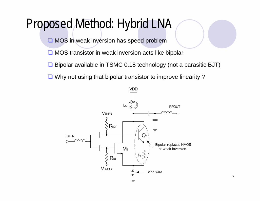
Proposed Method: Hybrid LNA
reRB1
RFIN
RB2
VBNPN
VBMOS
VDD
Ld RFOUT
Bond wire
Bipolar replaces NMOSat weak inversion.M1
Q2
MOS in weak inversion has speed problem
MOS transistor in weak inversion acts like bipolar
Bipolar available in TSMC 0.18 technology (not a parasitic BJT)
Why not using that bipolar transistor to improve linearity ?

8
Linearity Analysis of the BJT
Bipolar is more non-linear than MOS
Degeneration used to match the 3rd order non-linear term of MOST
πCπv
ev⎟⎟⎠
⎞⎜⎜⎝
⎛ −=
t
eiQo
vvIiφ
exp
er
oiiv
brbi
µC
re
oi
iv
Weak memory effect
-0.15
-0.10
-0.05
0.00
0.05
0.10
0.15
0.20
0.60 0.65 0.70 0.75 0.80 0.85 0.90 0.95 1.00Bias voltage (V)
3rd
orde
r coe
ffici
ent
3GHz
DC
( )( )em
em
m
Qbjt rg
rgg
Ig 21
161
5
3
2,3 −+
=

9
3rd Order Cancellation Effect
-0.30
-0.22
-0.14
-0.06
0.02
0.10
0.18
0.26
0.34
-0.16 -0.12 -0.08 -0.04 0.00 0.04 0.08 0.12 0.16
g 3(A
/V )3
g3,NPN
Input voltage (V)
g3,MOS g3
re
M1
Q2
MOS and BJT biased separately
MOS in moderate inversion, BJT in active region
The Goal!

10
Effects on Input Impedance Matching and Noise
LS
Lg
Ct gπ Vgs
gmVgs
Zin
-36
-34
-32
-30
-28
-26
-24
-22
-20
-18
2.80 2.85 2.90 2.95 3.00 3.05 3.10 3.15 3.20
BJT Enabled
BJT Disabled
Frequency (GHz)
S11(
dB)
πCCC gst += 1
πC shifts the matching point to a lower frequency
πg moves the impedance away from the intended value
BJT biased at low current: 320uA
BJT noise contribution: 2.4%
23.6%Other2.4%Bipolar Transistor14%MOS Transistor60%Source Resistance
Noise ratioDevice

11
Biasing Temperature Profile
0.66
0.69
0.72
0.75
0.78
0.81
0.84
-10 0 10 20 30 40 50 60 70 80 90 100
NPN
opt
imal
bia
s (V
)
Temperature ( C)
MOS biased by constant-gm
BJT biased by a PTAT circuit

12
Experimental Results of the Proposed Linearized LNA
-16
-12
-8
-4
0
4
8
2.5 2.55 2.6 2.65 2.7 2.75 2.8 2.85 2.9
S21
S22
S11
S12
Frequency (GHz)
S-pa
ram
eter
s (d
B)
-95
-75
-55
-35
-15
5
25
-30 -25 -20 -15 -10 -5 0 5 10 15 20
IIP3=14.5dBm
Input power (dBm)
Out
put
pow
er (
dBm
)
mW8.9PddB2.1NF
dBm14.5IIP3dB6.4Gain
GHz2.7Frequency
Active area: 390um x 290um

13
Extend to a Differential Version
678
910111213
141516
0.3 0.35 0.4 0.45 0.5 0.55 0.6 0.65 0.7678
910111213
141516
Auxilliary gate bias, Vaux (V)
IIP2IIP3
Vmain=0.74V
IIP3
(dB
m)
IIP2
(dB
m)
Single-ended suffers from small IIP2
Out-of-band termination
( ) ( ) ( )⎥⎦⎤
⎢⎣
⎡+
+∆+
=∆ωω
ωω2
12322, 2
2 gggggg
mmoB
The 3rd order term of MOS and BJT differential pair has the same sign.
BJT is more non-linear than MOS
Less current for BJT to present same non-linearity as MOS
Cross-couple MOS and BJT differential pair will help
( )( ) ( ) ( )ωωεωω
ωω2,6
123 31
12∆⋅⋅⋅
=−AHR
IIPs
( ) ( )ωωωωε 2,2, 3 ∆−=∆ oBgg

14
M1 M2
Q1 Q2
re re
VDD
VOUT+
VIN-
LD LD
VIN+
IEE ISS
VOUT-
MB1 MB2 MB3 MB4
-1.60
-1.20
-0.80
-0.40
0.00
0.40
0.80
1.20
-300 -200 -100 0 100 200 300
Input voltage (mV)
IM3
(A/V
^3)
BJT
BJT+NMOS
NMOS
-120
-80
-40
0
40
80
120
-300 -220 -140 -60 20 100 180 260
Input voltage (mV)
IM2
(mA/
V^2)
NMOS
BJT+NMOS
Extended flatnessfor small IM2
BJT
Extend to a Differential Version (Cont’d)
BJT pair contributes 15% of noiseLarger noise figure: 3.4 dBLarger current dissipation: 10mABetter reverse isolation: 25 dBNo need out-of-band termination

15
Experimental Results of the Proposed Differential LNA
-100
-80
-60
-40
-20
0
20
40
-30 -25 -20 -15 -10 -5 0 5 10 15
IIP3 with BJT enabled: 12.3 dBm
IIP3 with BJT disabled: 7.3 dBm
12.5 dB
Input power (dBm)
Out
put
pow
er (
dBm
)
-40
-35
-30
-25
-20
-15
-10
-5
0
5
10
15
2.3 2.35 2.4 2.45 2.5 2.55 2.6 2.65 2.7
S21
S22S11
S12
Frequency (GHz)
S- p
aram
eter
s (d
B)
mW19.8PddB3.4NF
dBm12.5IIP3dB10Gain
GHz2.5Frequency

16
IM3 Cancellation Demo
Measurement video clip shows the IM3 cancellation effect of BJT differential pair in the differential LNA.
SMIQ03
Test board
SMIQ03
FSEB30
Powercombiner
Measurement setup
17
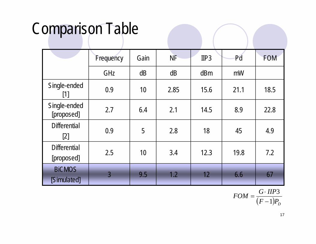
Comparison Table
7.219.812.33.4102.5Differential[proposed]
676.6121.29.53BiCMOS
[Simulated]
4.945182.850.9Differential
[2]
22.88.914.52.16.42.7Single-ended [proposed]
18.521.115.62.85100.9Single-ended [1]
mWdBmdBdBGHz
FOMPdIIP3NFGainFrequency
( ) DPFIIPGFOM1
3−⋅
=
18
Conclusions
Hybrid: Bipolar linearizes MOST
Differential structure: no degradation on IIP2
Better trade-offs between design parameters
Good figure of merit