
LMR64010 SIMPLE SWITCHER 40Vout, 1A Step-UpVoltage Regulator ... · LMR64010 SNVS736B – SEPTEMBER...
26
LMR64010 www.ti.com SNVS736B – SEPTEMBER 2011 – REVISED APRIL 2013 LMR64010 SIMPLE SWITCHER ® 40Vout, 1A Step-Up Voltage Regulator in SOT-23 Check for Samples: LMR64010 1FEATURES DESCRIPTION The LMR64010 switching regulators is a current- 2• Input Voltage Range of 2.7V to 14V mode boost converter operating at a fixed frequency • Output Voltage up to 40V of 1.6 MHz. • Switch Current up to 1A The use of SOT-23 package, made possible by the • 1.6 MHz Switching Frequency minimal power loss of the internal 1A switch, and use • Low Shutdown Iq, <1 μA of small inductors and capacitors result in the industry's highest power density. The 40V internal • Cycle-by-Cycle Current Limiting switch makes these solutions perfect for boosting to • Internally Compensated voltages of 16V or greater. • SOT-23-5 Packaging (2.92 x 2.84 x 1.08mm) These parts have a logic-level shutdown pin that can • Fully Enabled for WEBENCH® Power Designer be used to reduce quiescent current and extend battery life. PERFORMANCE BENEFITS Protection is provided through cycle-by-cycle current • Extremely Easy to Use limiting and thermal shutdown. Internal compensation simplifies design and reduces component count. • Tiny Overall Solution Reduces System Cost APPLICATIONS • Boost Conversions from 3.3V, 5V, and 12V Rails • Space Constrained Applications • Embedded Systems • LCD Displays • LED Applications System Performance 1 Please be aware that an important notice concerning availability, standard warranty, and use in critical applications of Texas Instruments semiconductor products and disclaimers thereto appears at the end of this data sheet. 2All trademarks are the property of their respective owners. PRODUCTION DATA information is current as of publication date. Copyright © 2011–2013, Texas Instruments Incorporated Products conform to specifications per the terms of the Texas Instruments standard warranty. Production processing does not necessarily include testing of all parameters.
-
Upload
nguyenngoc -
Category
Documents
-
view
217 -
download
0
Transcript of LMR64010 SIMPLE SWITCHER 40Vout, 1A Step-UpVoltage Regulator ... · LMR64010 SNVS736B – SEPTEMBER...
LMR64010
www.ti.com SNVS736B –SEPTEMBER 2011–REVISED APRIL 2013
LMR64010 SIMPLE SWITCHER® 40Vout, 1A Step-Up Voltage Regulator in SOT-23Check for Samples: LMR64010
1FEATURES DESCRIPTIONThe LMR64010 switching regulators is a current-
2• Input Voltage Range of 2.7V to 14Vmode boost converter operating at a fixed frequency
• Output Voltage up to 40V of 1.6 MHz.• Switch Current up to 1A
The use of SOT-23 package, made possible by the• 1.6 MHz Switching Frequency minimal power loss of the internal 1A switch, and use• Low Shutdown Iq, <1 µA of small inductors and capacitors result in the
industry's highest power density. The 40V internal• Cycle-by-Cycle Current Limitingswitch makes these solutions perfect for boosting to
• Internally Compensated voltages of 16V or greater.• SOT-23-5 Packaging (2.92 x 2.84 x 1.08mm)
These parts have a logic-level shutdown pin that can• Fully Enabled for WEBENCH® Power Designer be used to reduce quiescent current and extend
battery life.PERFORMANCE BENEFITS
Protection is provided through cycle-by-cycle current• Extremely Easy to Use limiting and thermal shutdown. Internal compensation
simplifies design and reduces component count.• Tiny Overall Solution Reduces System Cost
APPLICATIONS• Boost Conversions from 3.3V, 5V, and 12V
Rails• Space Constrained Applications• Embedded Systems• LCD Displays• LED Applications
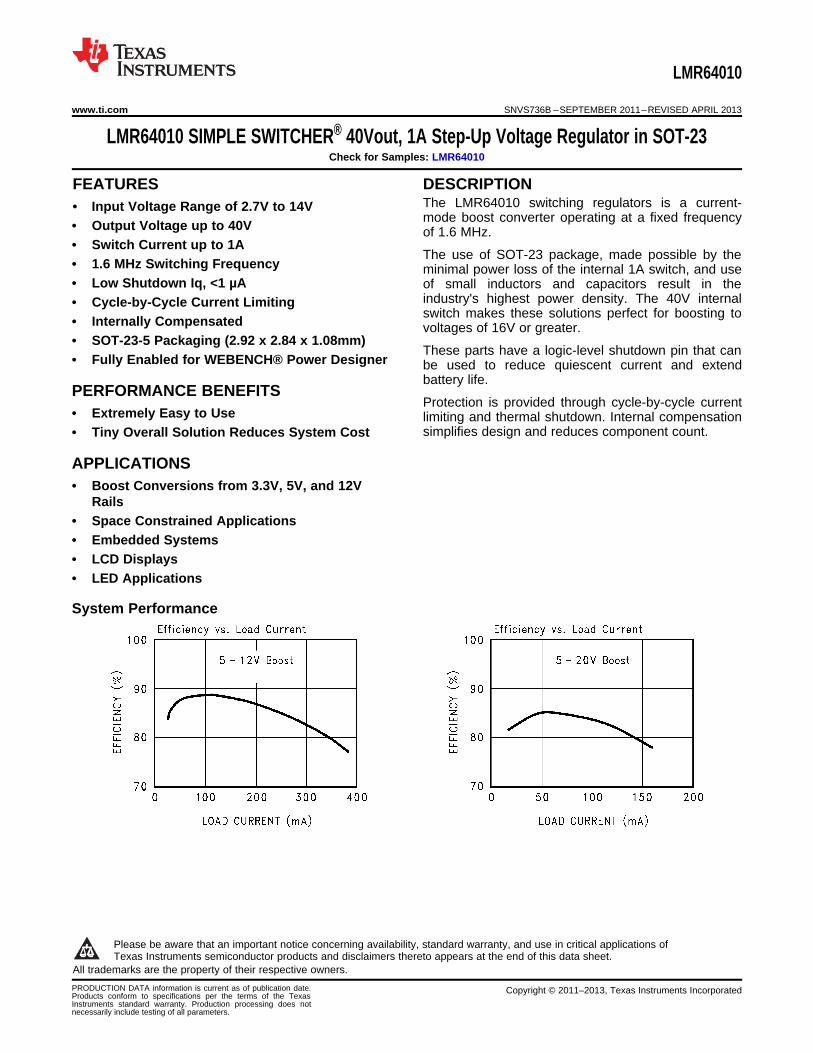
System Performance
1
Please be aware that an important notice concerning availability, standard warranty, and use in critical applications ofTexas Instruments semiconductor products and disclaimers thereto appears at the end of this data sheet.
2All trademarks are the property of their respective owners.
PRODUCTION DATA information is current as of publication date. Copyright © 2011–2013, Texas Instruments IncorporatedProducts conform to specifications per the terms of the TexasInstruments standard warranty. Production processing does notnecessarily include testing of all parameters.

LMR64010
SW
FB
GND
VIN
SHDN
U1
R351kSHDN
GND
5VIN
C12.2 PF
L1/10 PH
R213.3k
CF120 pF
D1
R1/205k
C24.7 PF
20VOUT
170 mA(TYP)
LMR64010
SNVS736B –SEPTEMBER 2011–REVISED APRIL 2013 www.ti.com
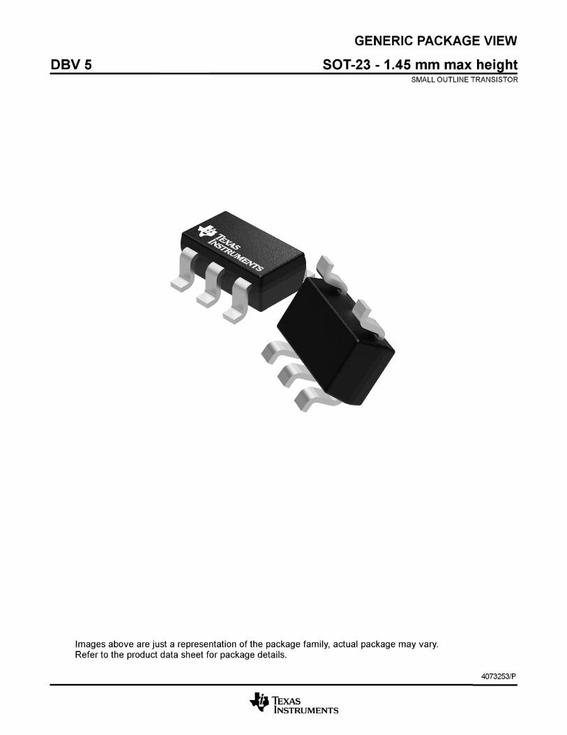
Top View
Figure 1. 5-Lead SOT-23 PackageSee Package Number DBV0005A
PIN DESCRIPTIONSPin Name Function
1 SW Drain of the internal FET switch.
2 GND Analog and power ground.
3 FB Feedback point that connects to external resistive divider.
4 SHDN Shutdown control input. Connect to VIN if this feature is not used.
5 VIN Analog and power input.
2 Submit Documentation Feedback Copyright © 2011–2013, Texas Instruments Incorporated
Product Folder Links: LMR64010

formula: If power dissipation exceeds the maximum specified above, the internal thermal protection
LMR64010
www.ti.com SNVS736B –SEPTEMBER 2011–REVISED APRIL 2013
These devices have limited built-in ESD protection. The leads should be shorted together or the device placed in conductive foamduring storage or handling to prevent electrostatic damage to the MOS gates.
Absolute Maximum Ratings (1) (2)
Storage Temperature Range −65°C to +150°C
Operating JunctionTemperature Range −40°C to +125°C
Lead Temp. (Soldering, 5 sec.) 300°C
Power Dissipation (3) Internally Limited
FB Pin Voltage −0.4V to +6V
SW Pin Voltage −0.4V to +40V
Input Supply Voltage −0.4V to +14.5V
SHDN Pin Voltage −0.4V to VIN + 0.3V
θJ-A (SOT-23-5) 265°C/W
ESD Rating (4) Human Body Model 2 kV
Machine Model 200V
For soldering specifications: http://www.ti.com/lit/SNOA549
(1) Absolute Maximum Ratings indicate limits beyond which damage to the component may occur. Electrical specifications do not applywhen operating the device outside of the limits set forth under the operating ratings which specify the intended range of operatingconditions.
(2) If Military/Aerospace specified devices are required, please contact the Texas Instruments Sales Office/ Distributors for availability andspecifications.
(3) The maximum power dissipation which can be safely dissipated for any application is a function of the maximum junction temperature,TJ(MAX) = 125°C, the junction-to-ambient thermal resistance for the SOT-23 package, θJ-A = 265°C/W, and the ambient temperature,TA. The maximum allowable power dissipation at any ambient temperature for designs using this device can be calculated using the
circuitry will protect the device by reducing the output voltage as required to maintain a safe junction temperature.(4) The human body model is a 100 pF capacitor discharged through a 1.5 kΩ resistor into each pin. The machine model is a 200 pF
capacitor discharged directly into each pin.
Copyright © 2011–2013, Texas Instruments Incorporated Submit Documentation Feedback 3
Product Folder Links: LMR64010
LMR64010
SNVS736B –SEPTEMBER 2011–REVISED APRIL 2013 www.ti.com
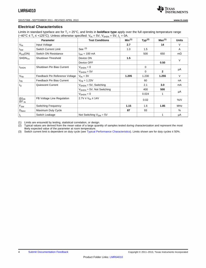
Electrical CharacteristicsLimits in standard typeface are for TJ = 25°C, and limits in boldface type apply over the full operating temperature range(−40°C ≤ TJ ≤ +125°C). Unless otherwise specified: VIN = 5V, VSHDN = 5V, IL = 0A.
Parameter Test Conditions Min (1) Typ (2) Max (1) Units
VIN Input Voltage 2.7 14 V
ISW Switch Current Limit See (3) 1.0 1.5 A
RDS(ON) Switch ON Resistance ISW = 100 mA 500 650 mΩSHDNTH Shutdown Threshold Device ON 1.5
VDevice OFF 0.50
ISHDN Shutdown Pin Bias Current VSHDN = 0 0µA
VSHDN = 5V 0 2
VFB Feedback Pin Reference Voltage VIN = 3V 1.205 1.230 1.255 V
IFB Feedback Pin Bias Current VFB = 1.23V 60 nA
IQ Quiescent Current VSHDN = 5V, Switching 2.1 3.0 mA
VSHDN = 5V, Not Switching 400 500µA
VSHDN = 0 0.024 1
ΔVFB FB Voltage Line Regulation 2.7V ≤ VIN ≤ 14V 0.02 %/VΔV IN
FSW Switching Frequency 1.15 1.6 1.85 MHz
DMAX Maximum Duty Cycle 87 93 %
IL Switch Leakage Not Switching VSW = 5V 1 µA
(1) Limits are ensuredd by testing, statistical correlation, or design.(2) Typical values are derived from the mean value of a large quantity of samples tested during characterization and represent the most
likely expected value of the parameter at room temperature.(3) Switch current limit is dependent on duty cycle (see Typical Performance Characteristics). Limits shown are for duty cycles ≤ 50%.
4 Submit Documentation Feedback Copyright © 2011–2013, Texas Instruments Incorporated
Product Folder Links: LMR64010

-40 -25 0 25 50 75 100 125
TEMPERATURE (oC)
92.7
92.8
92.9
93.0
93.1
93.2
93.3
93.4
MA
X D
UT
Y C
YC
LE (
%)
LMR64010
www.ti.com SNVS736B –SEPTEMBER 2011–REVISED APRIL 2013
Typical Performance CharacteristicsUnless otherwise specified: VIN = 5V, SHDN pin is tied to VIN.
Iq VIN (Active) vs Temperature Oscillator Frequency vs Temperature
Figure 2. Figure 3.
Max. Duty Cycle vs Temperature Feedback Voltage vs Temperature
Figure 4. Figure 5.
RDS(ON) vs Temperature Current Limit vs Temperature
Figure 6. Figure 7.
Copyright © 2011–2013, Texas Instruments Incorporated Submit Documentation Feedback 5
Product Folder Links: LMR64010

0 50 100 150 200 250 300 350
0
10
20
30
40
50
60
70
80
90
100
VIN = 10V
VIN = 5V
LOAD CURRENT (mA)
EF
FIC
IEN
CY
(%
)
0 50 100 150 200 250 300 350 400
0
10
20
30
40
50
60
70
80
90
100
VIN = 10V
VIN = 5V
LOAD CURRENT (mA)
EF
FIC
IEN
CY
(%
)
0 100 200 300 400 500 600 700
0
10
20
30
40
50
60
70
80
90
100
VIN = 10V
VIN = 5V
VIN = 3.3V
LOAD CURRENT (mA)
EF
FIC
IEN
CY
(%
)
LOAD CURRENT (mA)
EF
FIC
IEN
CY
(%
)
0 200 400 600 800 10000
10
20
30
40
50
60
70
80
90
100
VIN = 10VVIN = 5V
VIN = 3.3V
LMR64010
SNVS736B –SEPTEMBER 2011–REVISED APRIL 2013 www.ti.com
Typical Performance Characteristics (continued)Unless otherwise specified: VIN = 5V, SHDN pin is tied to VIN.
RDS(ON) vs VIN Efficiency vs Load Current (VOUT = 12V)
Figure 8. Figure 9.
Efficiency vs Load Current (VOUT = 15V) Efficiency vs Load Current (VOUT = 20V)
Figure 10. Figure 11.
Efficiency vs Load Current (VOUT = 25V) Efficiency vs Load Current (VOUT = 30V)
Figure 12. Figure 13.
6 Submit Documentation Feedback Copyright © 2011–2013, Texas Instruments Incorporated
Product Folder Links: LMR64010

0 50 100 150 2000
10
20
30
40
50
60
70
80
90
100
VIN = 10V
LOAD CURRENT (mA)
EF
FIC
IEN
CY
(%
)
0 50 100 150 200
LOAD CURRENT (mA)
EF
FIC
IEN
CY
(%
)
0
10
20
30
40
50
60
70
80
90
VIN=10V
LMR64010
www.ti.com SNVS736B –SEPTEMBER 2011–REVISED APRIL 2013
Typical Performance Characteristics (continued)Unless otherwise specified: VIN = 5V, SHDN pin is tied to VIN.
Efficiency vs Load Current (VOUT = 35V) Efficiency vs Load Current (VOUT = 40V)
Figure 14. Figure 15.
Block Diagram
Copyright © 2011–2013, Texas Instruments Incorporated Submit Documentation Feedback 7
Product Folder Links: LMR64010

LMR64010
SNVS736B –SEPTEMBER 2011–REVISED APRIL 2013 www.ti.com
APPLICATION INFORMATION
Theory of Operation
The LMR64010 is a switching converter IC that operates at a fixed frequency (1.6 MHz) using current-modecontrol for fast transient response over a wide input voltage range and incorporates pulse-by-pulse currentlimiting protection. Because this is current mode control, a 50 mΩ sense resistor in series with the switch FET isused to provide a voltage (which is proportional to the FET current) to both the input of the pulse widthmodulation (PWM) comparator and the current limit amplifier.
At the beginning of each cycle, the S-R latch turns on the FET. As the current through the FET increases, avoltage (proportional to this current) is summed with the ramp coming from the ramp generator and then fed intothe input of the PWM comparator. When this voltage exceeds the voltage on the other input (coming from theGm amplifier), the latch resets and turns the FET off. Since the signal coming from the Gm amplifier is derivedfrom the feedback (which samples the voltage at the output), the action of the PWM comparator constantly setsthe correct peak current through the FET to keep the output volatge in regulation.
Q1 and Q2 along with R3 - R6 form a bandgap voltage reference used by the IC to hold the output in regulation.The currents flowing through Q1 and Q2 will be equal, and the feedback loop will adjust the regulated output tomaintain this. Because of this, the regulated output is always maintained at a voltage level equal to the voltage atthe FB node "multiplied up" by the ratio of the output resistive divider.
The current limit comparator feeds directly into the flip-flop, that drives the switch FET. If the FET current reachesthe limit threshold, the FET is turned off and the cycle terminated until the next clock pulse. The current limitinput terminates the pulse regardless of the status of the output of the PWM comparator.
Application Hints
SELECTING THE EXTERNAL CAPACITORS
The best capacitors for use with the LMR64010 are multi-layer ceramic capacitors. They have the lowest ESR(equivalent series resistance) and highest resonance frequency which makes them optimum for use with highfrequency switching converters.
When selecting a ceramic capacitor, only X5R and X7R dielectric types should be used. Other types such asZ5U and Y5F have such severe loss of capacitance due to effects of temperature variation and applied voltage,they may provide as little as 20% of rated capacitance in many typical applications. Always consult capacitormanufacturer’s data curves before selecting a capacitor.
SELECTING THE OUTPUT CAPACITOR
A single ceramic capacitor of value 4.7 µF to 10 µF will provide sufficient output capacitance for mostapplications. For output voltages below 10V, a 10 µF capacitance is required. If larger amounts of capacitanceare desired for improved line support and transient response, tantalum capacitors can be used in parallel with theceramics. Aluminum electrolytics with ultra low ESR such as Sanyo Oscon can be used, but are usuallyprohibitively expensive. Typical AI electrolytic capacitors are not suitable for switching frequencies above 500kHz due to significant ringing and temperature rise due to self-heating from ripple current. An output capacitorwith excessive ESR can also reduce phase margin and cause instability.
SELECTING THE INPUT CAPACITOR
An input capacitor is required to serve as an energy reservoir for the current which must flow into the coil eachtime the switch turns ON. This capacitor must have extremely low ESR, so ceramic is the best choice. Werecommend a nominal value of 2.2 µF, but larger values can be used. Since this capacitor reduces the amount ofvoltage ripple seen at the input pin, it also reduces the amount of EMI passed back along that line to othercircuitry.
8 Submit Documentation Feedback Copyright © 2011–2013, Texas Instruments Incorporated
Product Folder Links: LMR64010
LMR64010
www.ti.com SNVS736B –SEPTEMBER 2011–REVISED APRIL 2013
FEED-FORWARD COMPENSATION
Although internally compensated, the feed-forward capacitor Cf is required for stability (see Basic ApplicationCircuit). Adding this capacitor puts a zero in the loop response of the converter. Without it, the regulator loop canoscillate. The recommended frequency for the zero fz should be approximately 8 kHz. Cf can be calculated usingthe formula:
Cf = 1 / (2 X π X R1 X fz) (1)
SELECTING DIODES
The external diode used in the typical application should be a Schottky diode. If the switch voltage is less than15V, a 20V diode such as the MBR0520 is recommended. If the switch voltage is between 15V and 25V, a 30Vdiode such as the MBR0530 is recommended. If the switch voltage exceeds 25V, a 40V diode such as theMBR0540 should be used.
The MBR05XX series of diodes are designed to handle a maximum average current of 0.5A. For applicationsexceeding 0.5A average but less than 1A, a Toshiba CRS08 can be used.
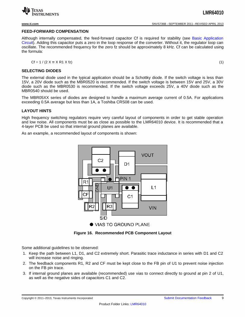
LAYOUT HINTS
High frequency switching regulators require very careful layout of components in order to get stable operationand low noise. All components must be as close as possible to the LMR64010 device. It is recommended that a4-layer PCB be used so that internal ground planes are available.
As an example, a recommended layout of components is shown:
Figure 16. Recommended PCB Component Layout
Some additional guidelines to be observed:1. Keep the path between L1, D1, and C2 extremely short. Parasitic trace inductance in series with D1 and C2
will increase noise and ringing.2. The feedback components R1, R2 and CF must be kept close to the FB pin of U1 to prevent noise injection
on the FB pin trace.3. If internal ground planes are available (recommended) use vias to connect directly to ground at pin 2 of U1,
as well as the negative sides of capacitors C1 and C2.
Copyright © 2011–2013, Texas Instruments Incorporated Submit Documentation Feedback 9
Product Folder Links: LMR64010

Duty Cycle =VOUT + VDIODE - VIN
VOUT + VDIODE - VSW
LMR64010
SNVS736B –SEPTEMBER 2011–REVISED APRIL 2013 www.ti.com
SETTING THE OUTPUT VOLTAGE
The output voltage is set using the external resistors R1 and R2 (see Basic Application Circuit). A value ofapproximately 13.3 kΩ is recommended for R2 to establish a divider current of approximately 92 µA. R1 iscalculated using the formula:
R1 = R2 X (VOUT/1.23 − 1) (2)
Figure 17. Basic Application Circuit
DUTY CYCLE
The maximum duty cycle of the switching regulator determines the maximum boost ratio of output-to-inputvoltage that the converter can attain in continuous mode of operation. The duty cycle for a given boostapplication is defined as:
(3)
This applies for continuous mode operation.
The equation shown for calculating duty cycle incorporates terms for the FET switch voltage and diode forwardvoltage. The actual duty cycle measured in operation will also be affected slightly by other power losses in thecircuit such as wire losses in the inductor, switching losses, and capacitor ripple current losses from self-heating.Therefore, the actual (effective) duty cycle measured may be slightly higher than calculated to compensate forthese power losses. A good approximation for effctive duty cycle is :
DC (eff) = (1 - Efficiency x (VIN/VOUT))
where• the efficiency can be approximated from the curves provided. (4)
INDUCTANCE VALUE
The first question we are usually asked is: “How small can I make the inductor?” (because they are the largestsized component and usually the most costly). The answer is not simple and involves tradeoffs in performance.Larger inductors mean less inductor ripple current, which typically means less output voltage ripple (for a givensize of output capacitor). Larger inductors also mean more load power can be delivered because the energystored during each switching cycle is:
E =L/2 X (lp)2
where• “lp” is the peak inductor current. (5)
10 Submit Documentation Feedback Copyright © 2011–2013, Texas Instruments Incorporated
Product Folder Links: LMR64010

LMR64010
SW
FB
GND
VIN
SHDN
U1
R351kSHDN
GND
5VIN
C12.2 PF
R213.3k
CF220 pF
D1MBR0520
R1/117K
L1/10 PH
C24.7 PF
12VOUT
330 mA(TYP)
LMR64010
www.ti.com SNVS736B –SEPTEMBER 2011–REVISED APRIL 2013
An important point to observe is that the LMR64010 will limit its switch current based on peak current. Thismeans that since lp(max) is fixed, increasing L will increase the maximum amount of power available to the load.Conversely, using too little inductance may limit the amount of load current which can be drawn from the output.
Best performance is usually obtained when the converter is operated in “continuous” mode at the load currentrange of interest, typically giving better load regulation and less output ripple. Continuous operation is defined asnot allowing the inductor current to drop to zero during the cycle. It should be noted that all boost converters shiftover to discontinuous operation as the output load is reduced far enough, but a larger inductor stays “continuous”over a wider load current range.
To better understand these tradeoffs, a typical application circuit (5V to 12V boost with a 10 µH inductor) will beanalyzed. We will assume:
VIN = 5V, VOUT = 12V, VDIODE = 0.5V, VSW = 0.5V
Since the frequency is 1.6 MHz (nominal), the period is approximately 0.625 µs. The duty cycle will be 62.5%,which means the ON time of the switch is 0.390 µs. It should be noted that when the switch is ON, the voltageacross the inductor is approximately 4.5V.
Using the equation:V = L (di/dt) (6)
We can then calculate the di/dt rate of the inductor which is found to be 0.45 A/µs during the ON time. Usingthese facts, we can then show what the inductor current will look like during operation:
Figure 18. 10 µH Inductor Current,5V–12V Boost
During the 0.390 µs ON time, the inductor current ramps up 0.176A and ramps down an equal amount during theOFF time. This is defined as the inductor “ripple current”. It can also be seen that if the load current drops toabout 33 mA, the inductor current will begin touching the zero axis which means it will be in discontinuous mode.A similar analysis can be performed on any boost converter, to make sure the ripple current is reasonable andcontinuous operation will be maintained at the typical load current values.
Figure 19. Typical Application, 5V–12V Boost
Copyright © 2011–2013, Texas Instruments Incorporated Submit Documentation Feedback 11
Product Folder Links: LMR64010
ILOAD(max) = (1 - DC) x (ISW(max) - DC (VIN - VSW))
2fL
0 20 40 60 80 100
0
200
400
600
800
1000
1200
1400
1600
SW
ITC
H C
UR
RE
NT
LIM
IT (
mA
)
DUTY CYCLE (%) = [1 - EFF*(VIN/VOUT))]
VIN = 5V
VIN = 3.3V
VIN = 2.7V
LMR64010
SNVS736B –SEPTEMBER 2011–REVISED APRIL 2013 www.ti.com
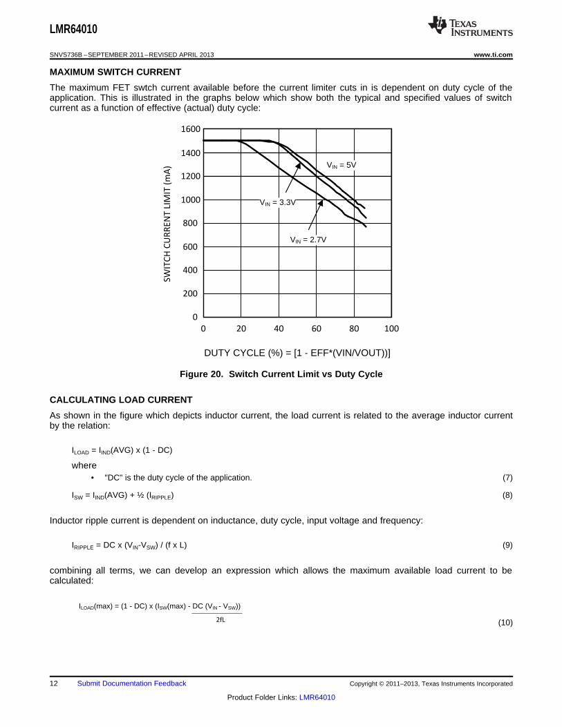
MAXIMUM SWITCH CURRENT
The maximum FET swtch current available before the current limiter cuts in is dependent on duty cycle of theapplication. This is illustrated in the graphs below which show both the typical and specified values of switchcurrent as a function of effective (actual) duty cycle:
Figure 20. Switch Current Limit vs Duty Cycle
CALCULATING LOAD CURRENT
As shown in the figure which depicts inductor current, the load current is related to the average inductor currentby the relation:
ILOAD = IIND(AVG) x (1 - DC)
where• "DC" is the duty cycle of the application. (7)
ISW = IIND(AVG) + ½ (IRIPPLE) (8)
Inductor ripple current is dependent on inductance, duty cycle, input voltage and frequency:
IRIPPLE = DC x (VIN-VSW) / (f x L) (9)
combining all terms, we can develop an expression which allows the maximum available load current to becalculated:
(10)
12 Submit Documentation Feedback Copyright © 2011–2013, Texas Instruments Incorporated
Product Folder Links: LMR64010

LMR64010
www.ti.com SNVS736B –SEPTEMBER 2011–REVISED APRIL 2013
The equation shown to calculate maximum load current takes into account the losses in the inductor or turn-OFFswitching losses of the FET and diode. For actual load current in typical applications, we took bench data forvarious input and output voltages and displayed the maximum load current available for a typical device in graphform:
Figure 21. Max. Load Current vs VIN
DESIGN PARAMETERS VSW AND ISW
The value of the FET "ON" voltage (referred to as VSW in the equations) is dependent on load current. A goodapproximation can be obtained by multiplying the "ON Resistance" of the FET times the average inductorcurrent.
FET on resistance increases at VIN values below 5V, since the internal N-FET has less gate voltage in this inputvoltage range (see Typical Performance Characteristics curves). Above VIN = 5V, the FET gate voltage isinternally clamped to 5V.
The maximum peak switch current the device can deliver is dependent on duty cycle. The minimum value isspecified to be > 1A at duty cycle below 50%. For higher duty cycles, see Typical Performance Characteristicscurves.
THERMAL CONSIDERATIONS
At higher duty cycles, the increased ON time of the FET means the maximum output current will be determinedby power dissipation within the LMR64010 FET switch. The switch power dissipation from ON-state conduction iscalculated by:
P(SW) = DC x IIND(AVE)2 x RDSON (11)
There will be some switching losses as well, so some derating needs to be applied when calculating IC powerdissipation.
Copyright © 2011–2013, Texas Instruments Incorporated Submit Documentation Feedback 13
Product Folder Links: LMR64010

LMR64010
SNVS736B –SEPTEMBER 2011–REVISED APRIL 2013 www.ti.com
MINIMUM INDUCTANCE
In some applications where the maximum load current is relatively small, it may be advantageous to use thesmallest possible inductance value for cost and size savings. The converter will operate in discontinuous mode insuch a case.
The minimum inductance should be selected such that the inductor (switch) current peak on each cycle does notreach the 1A current limit maximum. To understand how to do this, an example will be presented.
In the example, minimum switching frequency of 1.15 MHz will be used. This means the maximum cycle periodis the reciprocal of the minimum frequency:
TON(max) = 1/1.15M = 0.870 µs (12)
We will assume the input voltage is 5V, VOUT = 12V, VSW = 0.2V, VDIODE = 0.3V. The duty cycle is:
Duty Cycle = 60.3%
Therefore, the maximum switch ON time is 0.524 µs. An inductor should be selected with enough inductance toprevent the switch current from reaching 1A in the 0.524 µs ON time interval (see below):
Figure 22. Discontinuous Design, 5V–12V Boost
The voltage across the inductor during ON time is 4.8V. Minimum inductance value is found by:
V = L X dl/dt, L = V X (dt/dl) = 4.8 (0.524µ/1) = 2.5 µH (13)
In this case, a 2.7 µH inductor could be used assuming it provided at least that much inductance up to the 1Acurrent value. This same analysis can be used to find the minimum inductance for any boost application.
When selecting an inductor, make certain that the continuous current rating is high enough to avoid saturation atpeak currents. A suitable core type must be used to minimize core (switching) losses, and wire power lossesmust be considered when selecting the current rating.
SHUTDOWN PIN OPERATION
The device is turned off by pulling the shutdown pin low. If this function is not going to be used, the pin should betied directly to VIN. If the SHDN function will be needed, a pull-up resistor must be used to VIN (approximately50k-100kΩ recommended). The SHDN pin must not be left unterminated.
14 Submit Documentation Feedback Copyright © 2011–2013, Texas Instruments Incorporated
Product Folder Links: LMR64010
LMR64010
www.ti.com SNVS736B –SEPTEMBER 2011–REVISED APRIL 2013
REVISION HISTORY
Changes from Revision A (April 2013) to Revision B Page
• Changed layout of National Data Sheet to TI format .......................................................................................................... 14
Copyright © 2011–2013, Texas Instruments Incorporated Submit Documentation Feedback 15
Product Folder Links: LMR64010
PACKAGE OPTION ADDENDUM
www.ti.com 11-Apr-2013
Addendum-Page 1
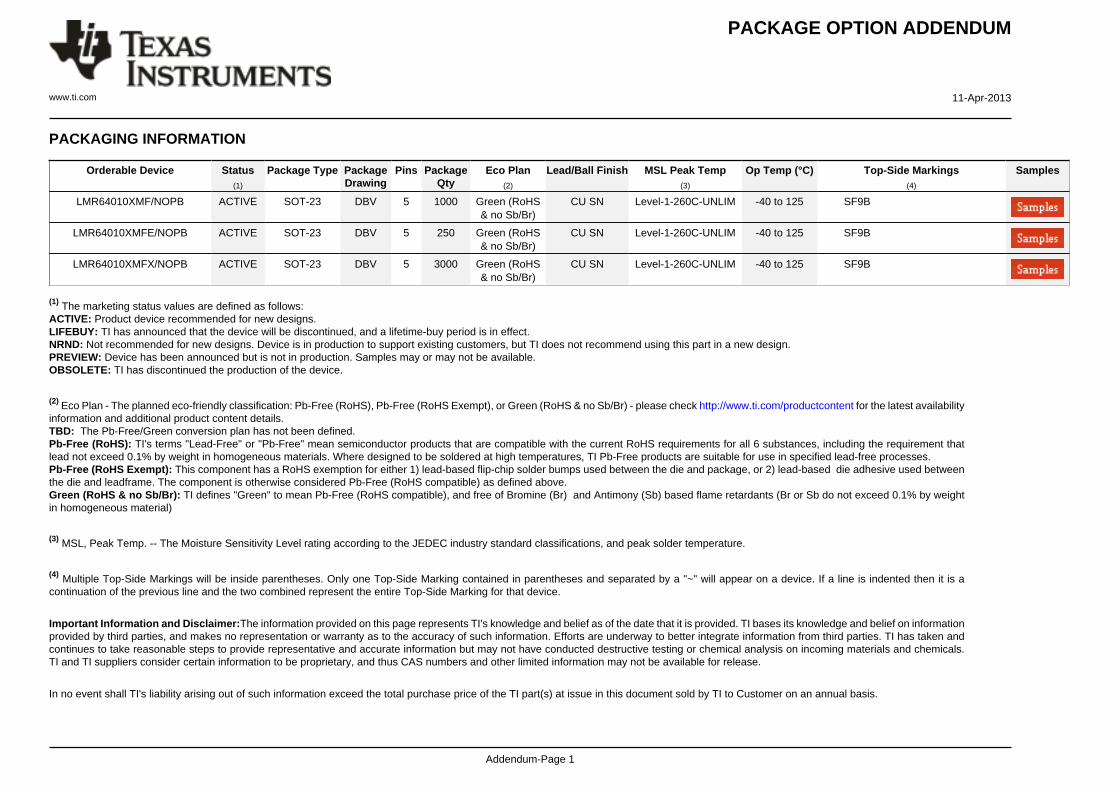
PACKAGING INFORMATION
Orderable Device Status(1)
Package Type PackageDrawing
Pins PackageQty
Eco Plan(2)
Lead/Ball Finish MSL Peak Temp(3)
Op Temp (°C) Top-Side Markings(4)
Samples
LMR64010XMF/NOPB ACTIVE SOT-23 DBV 5 1000 Green (RoHS& no Sb/Br)
CU SN Level-1-260C-UNLIM -40 to 125 SF9B
LMR64010XMFE/NOPB ACTIVE SOT-23 DBV 5 250 Green (RoHS& no Sb/Br)
CU SN Level-1-260C-UNLIM -40 to 125 SF9B
LMR64010XMFX/NOPB ACTIVE SOT-23 DBV 5 3000 Green (RoHS& no Sb/Br)
CU SN Level-1-260C-UNLIM -40 to 125 SF9B
(1) The marketing status values are defined as follows:ACTIVE: Product device recommended for new designs.LIFEBUY: TI has announced that the device will be discontinued, and a lifetime-buy period is in effect.NRND: Not recommended for new designs. Device is in production to support existing customers, but TI does not recommend using this part in a new design.PREVIEW: Device has been announced but is not in production. Samples may or may not be available.OBSOLETE: TI has discontinued the production of the device.
(2) Eco Plan - The planned eco-friendly classification: Pb-Free (RoHS), Pb-Free (RoHS Exempt), or Green (RoHS & no Sb/Br) - please check http://www.ti.com/productcontent for the latest availabilityinformation and additional product content details.TBD: The Pb-Free/Green conversion plan has not been defined.Pb-Free (RoHS): TI's terms "Lead-Free" or "Pb-Free" mean semiconductor products that are compatible with the current RoHS requirements for all 6 substances, including the requirement thatlead not exceed 0.1% by weight in homogeneous materials. Where designed to be soldered at high temperatures, TI Pb-Free products are suitable for use in specified lead-free processes.Pb-Free (RoHS Exempt): This component has a RoHS exemption for either 1) lead-based flip-chip solder bumps used between the die and package, or 2) lead-based die adhesive used betweenthe die and leadframe. The component is otherwise considered Pb-Free (RoHS compatible) as defined above.Green (RoHS & no Sb/Br): TI defines "Green" to mean Pb-Free (RoHS compatible), and free of Bromine (Br) and Antimony (Sb) based flame retardants (Br or Sb do not exceed 0.1% by weightin homogeneous material)
(3) MSL, Peak Temp. -- The Moisture Sensitivity Level rating according to the JEDEC industry standard classifications, and peak solder temperature.
(4) Multiple Top-Side Markings will be inside parentheses. Only one Top-Side Marking contained in parentheses and separated by a "~" will appear on a device. If a line is indented then it is acontinuation of the previous line and the two combined represent the entire Top-Side Marking for that device.
Important Information and Disclaimer:The information provided on this page represents TI's knowledge and belief as of the date that it is provided. TI bases its knowledge and belief on informationprovided by third parties, and makes no representation or warranty as to the accuracy of such information. Efforts are underway to better integrate information from third parties. TI has taken andcontinues to take reasonable steps to provide representative and accurate information but may not have conducted destructive testing or chemical analysis on incoming materials and chemicals.TI and TI suppliers consider certain information to be proprietary, and thus CAS numbers and other limited information may not be available for release.
In no event shall TI's liability arising out of such information exceed the total purchase price of the TI part(s) at issue in this document sold by TI to Customer on an annual basis.

TAPE AND REEL INFORMATION
*All dimensions are nominal
Device PackageType
PackageDrawing
Pins SPQ ReelDiameter
(mm)
ReelWidth
W1 (mm)
A0(mm)
B0(mm)
K0(mm)
P1(mm)
W(mm)
Pin1Quadrant
LMR64010XMF/NOPB SOT-23 DBV 5 1000 178.0 8.4 3.2 3.2 1.4 4.0 8.0 Q3
LMR64010XMFE/NOPB SOT-23 DBV 5 250 178.0 8.4 3.2 3.2 1.4 4.0 8.0 Q3
LMR64010XMFX/NOPB SOT-23 DBV 5 3000 178.0 8.4 3.2 3.2 1.4 4.0 8.0 Q3
PACKAGE MATERIALS INFORMATION
www.ti.com 20-Dec-2016
Pack Materials-Page 1

*All dimensions are nominal
Device Package Type Package Drawing Pins SPQ Length (mm) Width (mm) Height (mm)
LMR64010XMF/NOPB SOT-23 DBV 5 1000 210.0 185.0 35.0
LMR64010XMFE/NOPB SOT-23 DBV 5 250 210.0 185.0 35.0
LMR64010XMFX/NOPB SOT-23 DBV 5 3000 210.0 185.0 35.0
PACKAGE MATERIALS INFORMATION
www.ti.com 20-Dec-2016
Pack Materials-Page 2

www.ti.com
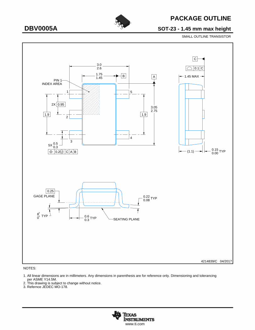
PACKAGE OUTLINE
C
TYP0.220.08
0.25
3.02.6
2X 0.95
1.9
1.45 MAX
TYP0.150.00
5X 0.50.3
TYP0.60.3
TYP80
1.9
A
3.052.75
B1.751.45
(1.1)
SOT-23 - 1.45 mm max heightDBV0005ASMALL OUTLINE TRANSISTOR
4214839/C 04/2017
NOTES: 1. All linear dimensions are in millimeters. Any dimensions in parenthesis are for reference only. Dimensioning and tolerancing per ASME Y14.5M.2. This drawing is subject to change without notice.3. Refernce JEDEC MO-178.
0.2 C A B
1
34
5
2
INDEX AREAPIN 1
GAGE PLANE
SEATING PLANE
0.1 C
SCALE 4.000

www.ti.com
EXAMPLE BOARD LAYOUT
0.07 MAXARROUND
0.07 MINARROUND
5X (1.1)
5X (0.6)
(2.6)
(1.9)
2X (0.95)
(R0.05) TYP
4214839/C 04/2017
SOT-23 - 1.45 mm max heightDBV0005ASMALL OUTLINE TRANSISTOR
NOTES: (continued) 4. Publication IPC-7351 may have alternate designs. 5. Solder mask tolerances between and around signal pads can vary based on board fabrication site.
SYMM
LAND PATTERN EXAMPLEEXPOSED METAL SHOWN
SCALE:15X
PKG
1
3 4
5
2
SOLDER MASKOPENINGMETAL UNDER
SOLDER MASK
SOLDER MASKDEFINED
EXPOSED METAL
METALSOLDER MASKOPENING
NON SOLDER MASKDEFINED
(PREFERRED)
SOLDER MASK DETAILS
EXPOSED METAL

www.ti.com
EXAMPLE STENCIL DESIGN
(2.6)
(1.9)
2X(0.95)
5X (1.1)
5X (0.6)
(R0.05) TYP
SOT-23 - 1.45 mm max heightDBV0005ASMALL OUTLINE TRANSISTOR
4214839/C 04/2017
NOTES: (continued) 6. Laser cutting apertures with trapezoidal walls and rounded corners may offer better paste release. IPC-7525 may have alternate design recommendations. 7. Board assembly site may have different recommendations for stencil design.
SOLDER PASTE EXAMPLEBASED ON 0.125 mm THICK STENCIL
SCALE:15X
SYMM
PKG
1
3 4
5
2
www.ti.com
PACKAGE OUTLINE
C
TYP0.220.08
0.25
3.02.6
2X 0.95
1.9
1.45 MAX
TYP0.150.00
5X 0.50.3
TYP0.60.3
TYP80
1.9
A
3.052.75
B1.751.45
(1.1)
SOT-23 - 1.45 mm max heightDBV0005ASMALL OUTLINE TRANSISTOR
4214839/C 04/2017
NOTES: 1. All linear dimensions are in millimeters. Any dimensions in parenthesis are for reference only. Dimensioning and tolerancing per ASME Y14.5M.2. This drawing is subject to change without notice.3. Refernce JEDEC MO-178.
0.2 C A B
1
34
5
2
INDEX AREAPIN 1
GAGE PLANE
SEATING PLANE
0.1 C
SCALE 4.000

www.ti.com
EXAMPLE BOARD LAYOUT
0.07 MAXARROUND
0.07 MINARROUND
5X (1.1)
5X (0.6)
(2.6)
(1.9)
2X (0.95)
(R0.05) TYP
4214839/C 04/2017
SOT-23 - 1.45 mm max heightDBV0005ASMALL OUTLINE TRANSISTOR
NOTES: (continued) 4. Publication IPC-7351 may have alternate designs. 5. Solder mask tolerances between and around signal pads can vary based on board fabrication site.
SYMM
LAND PATTERN EXAMPLEEXPOSED METAL SHOWN
SCALE:15X
PKG
1
3 4
5
2
SOLDER MASKOPENINGMETAL UNDER
SOLDER MASK
SOLDER MASKDEFINED
EXPOSED METAL
METALSOLDER MASKOPENING
NON SOLDER MASKDEFINED
(PREFERRED)
SOLDER MASK DETAILS
EXPOSED METAL

www.ti.com
EXAMPLE STENCIL DESIGN
(2.6)
(1.9)
2X(0.95)
5X (1.1)
5X (0.6)
(R0.05) TYP
SOT-23 - 1.45 mm max heightDBV0005ASMALL OUTLINE TRANSISTOR
4214839/C 04/2017
NOTES: (continued) 6. Laser cutting apertures with trapezoidal walls and rounded corners may offer better paste release. IPC-7525 may have alternate design recommendations. 7. Board assembly site may have different recommendations for stencil design.
SOLDER PASTE EXAMPLEBASED ON 0.125 mm THICK STENCIL
SCALE:15X
SYMM
PKG
1
3 4
5
2

IMPORTANT NOTICE
Texas Instruments Incorporated (TI) reserves the right to make corrections, enhancements, improvements and other changes to itssemiconductor products and services per JESD46, latest issue, and to discontinue any product or service per JESD48, latest issue. Buyersshould obtain the latest relevant information before placing orders and should verify that such information is current and complete.TI’s published terms of sale for semiconductor products (http://www.ti.com/sc/docs/stdterms.htm) apply to the sale of packaged integratedcircuit products that TI has qualified and released to market. Additional terms may apply to the use or sale of other types of TI products andservices.Reproduction of significant portions of TI information in TI data sheets is permissible only if reproduction is without alteration and isaccompanied by all associated warranties, conditions, limitations, and notices. TI is not responsible or liable for such reproduceddocumentation. Information of third parties may be subject to additional restrictions. Resale of TI products or services with statementsdifferent from or beyond the parameters stated by TI for that product or service voids all express and any implied warranties for theassociated TI product or service and is an unfair and deceptive business practice. TI is not responsible or liable for any such statements.Buyers and others who are developing systems that incorporate TI products (collectively, “Designers”) understand and agree that Designersremain responsible for using their independent analysis, evaluation and judgment in designing their applications and that Designers havefull and exclusive responsibility to assure the safety of Designers' applications and compliance of their applications (and of all TI productsused in or for Designers’ applications) with all applicable regulations, laws and other applicable requirements. Designer represents that, withrespect to their applications, Designer has all the necessary expertise to create and implement safeguards that (1) anticipate dangerousconsequences of failures, (2) monitor failures and their consequences, and (3) lessen the likelihood of failures that might cause harm andtake appropriate actions. Designer agrees that prior to using or distributing any applications that include TI products, Designer willthoroughly test such applications and the functionality of such TI products as used in such applications.TI’s provision of technical, application or other design advice, quality characterization, reliability data or other services or information,including, but not limited to, reference designs and materials relating to evaluation modules, (collectively, “TI Resources”) are intended toassist designers who are developing applications that incorporate TI products; by downloading, accessing or using TI Resources in anyway, Designer (individually or, if Designer is acting on behalf of a company, Designer’s company) agrees to use any particular TI Resourcesolely for this purpose and subject to the terms of this Notice.TI’s provision of TI Resources does not expand or otherwise alter TI’s applicable published warranties or warranty disclaimers for TIproducts, and no additional obligations or liabilities arise from TI providing such TI Resources. TI reserves the right to make corrections,enhancements, improvements and other changes to its TI Resources. TI has not conducted any testing other than that specificallydescribed in the published documentation for a particular TI Resource.Designer is authorized to use, copy and modify any individual TI Resource only in connection with the development of applications thatinclude the TI product(s) identified in such TI Resource. NO OTHER LICENSE, EXPRESS OR IMPLIED, BY ESTOPPEL OR OTHERWISETO ANY OTHER TI INTELLECTUAL PROPERTY RIGHT, AND NO LICENSE TO ANY TECHNOLOGY OR INTELLECTUAL PROPERTYRIGHT OF TI OR ANY THIRD PARTY IS GRANTED HEREIN, including but not limited to any patent right, copyright, mask work right, orother intellectual property right relating to any combination, machine, or process in which TI products or services are used. Informationregarding or referencing third-party products or services does not constitute a license to use such products or services, or a warranty orendorsement thereof. Use of TI Resources may require a license from a third party under the patents or other intellectual property of thethird party, or a license from TI under the patents or other intellectual property of TI.TI RESOURCES ARE PROVIDED “AS IS” AND WITH ALL FAULTS. TI DISCLAIMS ALL OTHER WARRANTIES ORREPRESENTATIONS, EXPRESS OR IMPLIED, REGARDING RESOURCES OR USE THEREOF, INCLUDING BUT NOT LIMITED TOACCURACY OR COMPLETENESS, TITLE, ANY EPIDEMIC FAILURE WARRANTY AND ANY IMPLIED WARRANTIES OFMERCHANTABILITY, FITNESS FOR A PARTICULAR PURPOSE, AND NON-INFRINGEMENT OF ANY THIRD PARTY INTELLECTUALPROPERTY RIGHTS. TI SHALL NOT BE LIABLE FOR AND SHALL NOT DEFEND OR INDEMNIFY DESIGNER AGAINST ANY CLAIM,INCLUDING BUT NOT LIMITED TO ANY INFRINGEMENT CLAIM THAT RELATES TO OR IS BASED ON ANY COMBINATION OFPRODUCTS EVEN IF DESCRIBED IN TI RESOURCES OR OTHERWISE. IN NO EVENT SHALL TI BE LIABLE FOR ANY ACTUAL,DIRECT, SPECIAL, COLLATERAL, INDIRECT, PUNITIVE, INCIDENTAL, CONSEQUENTIAL OR EXEMPLARY DAMAGES INCONNECTION WITH OR ARISING OUT OF TI RESOURCES OR USE THEREOF, AND REGARDLESS OF WHETHER TI HAS BEENADVISED OF THE POSSIBILITY OF SUCH DAMAGES.Unless TI has explicitly designated an individual product as meeting the requirements of a particular industry standard (e.g., ISO/TS 16949and ISO 26262), TI is not responsible for any failure to meet such industry standard requirements.Where TI specifically promotes products as facilitating functional safety or as compliant with industry functional safety standards, suchproducts are intended to help enable customers to design and create their own applications that meet applicable functional safety standardsand requirements. Using products in an application does not by itself establish any safety features in the application. Designers mustensure compliance with safety-related requirements and standards applicable to their applications. Designer may not use any TI products inlife-critical medical equipment unless authorized officers of the parties have executed a special contract specifically governing such use.Life-critical medical equipment is medical equipment where failure of such equipment would cause serious bodily injury or death (e.g., lifesupport, pacemakers, defibrillators, heart pumps, neurostimulators, and implantables). Such equipment includes, without limitation, allmedical devices identified by the U.S. Food and Drug Administration as Class III devices and equivalent classifications outside the U.S.TI may expressly designate certain products as completing a particular qualification (e.g., Q100, Military Grade, or Enhanced Product).Designers agree that it has the necessary expertise to select the product with the appropriate qualification designation for their applicationsand that proper product selection is at Designers’ own risk. Designers are solely responsible for compliance with all legal and regulatoryrequirements in connection with such selection.Designer will fully indemnify TI and its representatives against any damages, costs, losses, and/or liabilities arising out of Designer’s non-compliance with the terms and provisions of this Notice.
Mailing Address: Texas Instruments, Post Office Box 655303, Dallas, Texas 75265Copyright © 2018, Texas Instruments Incorporated


