
LMK03000 Family Precision Clock Conditioner with ... Family Precision Clock Conditioner with...
45
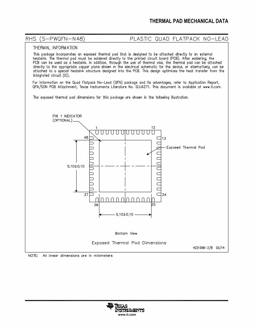
LMK0300xx Precision Clock Conditioner Recovered ‡GLUW\· FORFN RU clean clock 0XOWLSOH ‡FOHDQ· FORFNV DW different frequencies Fout CLKout7 CLKout4 CLKout1 CLKout0 DAC Serializer/ Deserializer LMX2531 PLL+VCO ADC > 1 Gsps FPGA OSCin LMK03000, LMK03000C, LMK03000D, LMK03001 LMK03001C, LMK03001D, LMK03033, LMK03033C www.ti.com SNAS381O – NOVEMBER 2006 – REVISED MARCH 2013 LMK03000 Family Precision Clock Conditioner with Integrated VCO Check for Samples: LMK03000, LMK03000C, LMK03000D, LMK03001, LMK03001C, LMK03001D, LMK03033, LMK03033C 1 FEATURES 12 • Integrated VCO with Very Low Phase Noise • Partially Integrated Loop Filter Floor • Dedicated Divider and Delay Blocks on Each • Integrated Integer-N PLL with Outstanding Clock Output Normalized Phase Noise Contribution of -224 • Pin Compatible Family of Clocking Devices dBc/Hz • 3.15 to 3.45 V Operation • VCO Divider Values of 2 to 8 (All Divides) • Package: 48 Pin WQFN (7.0 x 7.0 x 0.8 mm) • Channel Divider Values of 1, 2 to 510 (even • 200 fs RMS Clock Generator Performance (10 divides) Hz to 20 MHz) with a Clean Input Clock • LVDS and LVPECL Clock Outputs 1.1 TARGET APPLICATIONS VCO • Data Converter Clocking Device Outputs Tuning Range RMS Jitter • Networking, SONET/SDH, DSLAM (MHz) (fs) • Wireless Infrastructure LMK03000C 400 • Medical LMK03000 1185 - 1296 800 • Test and Measurement LMK03000D 1200 3 LVDS 5 LVPECL • Military / Aerospace LMK03001C 400 LMK03001 1470 - 1570 800 LMK03001D 1200 LMK03033C 500 4 LVDS 1843 - 2160 4 LVPECL LMK03033 800 1 Please be aware that an important notice concerning availability, standard warranty, and use in critical applications of Texas Instruments semiconductor products and disclaimers thereto appears at the end of this data sheet. 2All trademarks are the property of their respective owners. PRODUCTION DATA information is current as of publication date. Products conform to Copyright © 2006–2013, Texas Instruments Incorporated specifications per the terms of the Texas Instruments standard warranty. Production processing does not necessarily include testing of all parameters.
Transcript of LMK03000 Family Precision Clock Conditioner with ... Family Precision Clock Conditioner with...

LMK0300xx
Precision Clock Conditioner
Recovered ³GLUW\´FORFNRU
clean clock
0XOWLSOH³FOHDQ´FORFNVDW
different frequencies
Fout
CLKout7
CLKout4
CLKout1
CLKout0
DAC
Serializer/Deserializer
LMX2531PLL+VCO
ADC> 1 Gsps
FPGA
OSCin
LMK03000, LMK03000C, LMK03000D, LMK03001LMK03001C, LMK03001D, LMK03033, LMK03033C
www.ti.com SNAS381O –NOVEMBER 2006–REVISED MARCH 2013
LMK03000 Family Precision Clock Conditioner with Integrated VCOCheck for Samples: LMK03000, LMK03000C, LMK03000D, LMK03001, LMK03001C, LMK03001D, LMK03033, LMK03033C
1 FEATURES12
• Integrated VCO with Very Low Phase Noise • Partially Integrated Loop FilterFloor • Dedicated Divider and Delay Blocks on Each
• Integrated Integer-N PLL with Outstanding Clock OutputNormalized Phase Noise Contribution of -224 • Pin Compatible Family of Clocking DevicesdBc/Hz • 3.15 to 3.45 V Operation
• VCO Divider Values of 2 to 8 (All Divides) • Package: 48 Pin WQFN (7.0 x 7.0 x 0.8 mm)• Channel Divider Values of 1, 2 to 510 (even • 200 fs RMS Clock Generator Performance (10
divides) Hz to 20 MHz) with a Clean Input Clock• LVDS and LVPECL Clock Outputs
1.1 TARGET APPLICATIONSVCO• Data Converter Clocking
Device Outputs Tuning Range RMS Jitter• Networking, SONET/SDH, DSLAM(MHz) (fs)
• Wireless Infrastructure LMK03000C 400• Medical LMK03000 1185 - 1296 800• Test and Measurement LMK03000D 12003 LVDS
5 LVPECL• Military / Aerospace LMK03001C 400
LMK03001 1470 - 1570 800
LMK03001D 1200
LMK03033C 5004 LVDS 1843 - 21604 LVPECLLMK03033 800
1
Please be aware that an important notice concerning availability, standard warranty, and use in critical applications ofTexas Instruments semiconductor products and disclaimers thereto appears at the end of this data sheet.
2All trademarks are the property of their respective owners.
PRODUCTION DATA information is current as of publication date. Products conform to Copyright © 2006–2013, Texas Instruments Incorporatedspecifications per the terms of the Texas Instruments standard warranty. Productionprocessing does not necessarily include testing of all parameters.
LMK03000, LMK03000C, LMK03000D, LMK03001LMK03001C, LMK03001D, LMK03033, LMK03033CSNAS381O –NOVEMBER 2006–REVISED MARCH 2013 www.ti.com
1.2 DESCRIPTION
The LMK03000 family of precision clock conditioners combine the functions of jittercleaning/reconditioning, multiplication, and distribution of a reference clock. The devices integrate aVoltage Controlled Oscillator (VCO), a high performance Integer-N Phase Locked Loop (PLL), a partiallyintegrated loop filter, and up to eight outputs in various LVDS and LVPECL combinations.
The VCO output is optionally accessible on the Fout port. Internally, the VCO output goes through a VCODivider to feed the various clock distribution blocks.
Each clock distribution block includes a programmable divider, a phase synchronization circuit, aprogrammable delay, a clock output mux, and an LVDS or LVPECL output buffer. This allows multipleinteger-related and phase-adjusted copies of the reference to be distributed to eight system components.
The clock conditioners come in a 48-pin WQFN package and are footprint compatible with other clockingdevices in the same family.
1 FEATURES ............................................... 1 6.10 POWER ON RESET ............................... 17
1.1 TARGET APPLICATIONS ........................... 1 6.11 DIGITAL LOCK DETECT ........................... 18
1.2 DESCRIPTION ...................................... 2 7 General Programming Information ................ 192 Device Information ...................................... 3 7.1 RECOMMENDED PROGRAMMING SEQUENCE . 19
2.1 Functional Block Diagram ........................... 3 7.2 REGISTER R0 to R7 ............................... 22
2.2 Connection Diagram ................................. 4 7.3 REGISTER R8 ..................................... 24
3 Electrical Specifications ............................... 6 7.4 REGISTER R9 ...................................... 24
3.1 Absolute Maximum Ratings .......................... 6 7.5 REGISTER R11 .................................... 24
3.2 Recommended Operating Conditions ............... 6 7.6 REGISTER R13 .................................... 24
3.3 Package Thermal Resistance ....................... 6 7.7 REGISTER R14 .................................... 25
3.4 Electrical Characteristics ............................ 7 7.8 REGISTER R15 .................................... 27
3.5 Serial Data Timing Diagram ........................ 11 8 Application Information .............................. 284 Measurement Definitions ............................ 12 8.1 SYSTEM LEVEL DIAGRAM ........................ 28
4.1 Charge Pump Current Specification Definitions .... 12 8.2 BIAS PIN ........................................... 28
5 Typical Performance Characteristics ............. 13 8.3 LDO BYPASS ...................................... 28
6 Functional Description ............................... 15 8.4 LOOP FILTER ...................................... 298.5 CURRENT CONSUMPTION / POWER6.1 BIAS PIN ........................................... 15
DISSIPATION CALCULATIONS ................... 306.2 LDO BYPASS ...................................... 158.6 THERMAL MANAGEMENT ........................ 316.3 OSCILLATOR INPUT PORT (OSCin, OSCin*) .... 158.7 TERMINATION AND USE OF CLOCK OUTPUTS6.4 LOW NOISE, FULLY INTEGRATED VCO ......... 15
(DRIVERS) ......................................... 326.5 CLKout DELAYS ................................... 15
8.8 OSCin INPUT ...................................... 366.6 LVDS/LVPECL OUTPUTS ......................... 16 8.9 MORE THAN EIGHT OUTPUTS WITH AN6.7 GLOBAL CLOCK OUTPUT SYNCHRONIZATION 16 LMK03000 FAMILY DEVICE ....................... 376.8 CLKout OUTPUT STATES ......................... 17 Revision History ............................................ 386.9 GLOBAL OUTPUT ENABLE AND LOCK DETECT 17
2 Contents Copyright © 2006–2013, Texas Instruments Incorporated
Submit Documentation FeedbackProduct Folder Links: LMK03000 LMK03000C LMK03000D LMK03001 LMK03001C LMK03001D LMK03033
LMK03033C

OSCin
OSCin*R Divider
Phase Detector
N Divider
VCODivider
CLKout0CLKout0*
CLKout1CLKout1*
CLKout2CLKout2*
CLKout3CLKout3*
CLKout4CLKout4*
CLKout5CLKout5*
CLKout6CLKout6*
CLKout7CLKout7*
CP
out
Internal VCO
Partially Integrated Loop Filter
DividerDelay
Mux
DividerDelay
Mux
DividerDelay
Mux
DividerDelay
Mux
DividerDelay
Mux
DividerDelay
Mux
DividerDelay
Mux
DividerDelay
Mux
Distribution Path
CLK
DATA
LE
ControlRegisters
PWirePort
Device Control
LDGOE
SYNC*
Fout
Low Clock Buffers
High Clock Buffers
LMK03000, LMK03000C, LMK03000D, LMK03001LMK03001C, LMK03001D, LMK03033, LMK03033C
www.ti.com SNAS381O –NOVEMBER 2006–REVISED MARCH 2013
2 Device Information
2.1 Functional Block Diagram
Copyright © 2006–2013, Texas Instruments Incorporated Device Information 3Submit Documentation Feedback
Product Folder Links: LMK03000 LMK03000C LMK03000D LMK03001 LMK03001C LMK03001D LMK03033LMK03033C

4748 46 45 44 43 42 41 40 39 38 37
11
12
10
9
8
7
6
5
4
3
2
1
1413 15 16 17 18 19 20 21 22 23 24
26
25
27
28
29
30
31
32
33
34
35
36GND
Fout
Vcc1
Vcc2
Vcc
3
Vcc
4
Vcc
5
Vcc
6
Vcc7
Vcc8
Vcc9
Vcc10
Vcc
11
Vcc
12
Vcc
13
Vcc
14
CLKuWire
DATAuWire
LEuWire
NC
LDObyp1
LDObyp2
GOE
LD
CLK
out0
CLK
out0
*
CLK
out1
CLK
out1
*
CLK
out2
CLK
out2
*
CLK
out3
CLK
out3
*
GND
SYNC*
OSCin
OSCin*
CPout
NC
NC
Bias
CLK
out4
CLK
out4
*
CLK
out5
CLK
out5
*
CLK
out6
CLK
out6
*
CLK
out7
CLK
out7
*
DAP
Top Down View
LMK03000, LMK03000C, LMK03000D, LMK03001LMK03001C, LMK03001D, LMK03033, LMK03033CSNAS381O –NOVEMBER 2006–REVISED MARCH 2013 www.ti.com
2.2 Connection Diagram
Figure 2-1. 48-Pin WQFN Package
4 Device Information Copyright © 2006–2013, Texas Instruments Incorporated
Submit Documentation FeedbackProduct Folder Links: LMK03000 LMK03000C LMK03000D LMK03001 LMK03001C LMK03001D LMK03033
LMK03033C

LMK03000, LMK03000C, LMK03000D, LMK03001LMK03001C, LMK03001D, LMK03033, LMK03033C
www.ti.com SNAS381O –NOVEMBER 2006–REVISED MARCH 2013
Table 2-1. PIN DESCRIPTIONS
Pin # Pin Name I/O Description
1, 25 GND - Ground
2 Fout O Internal VCO Frequency Output
3, 8, 13, 16, 19, 22, Vcc1, Vcc2, Vcc3, Vcc4, Vcc5, Vcc6, Vcc7, Vcc8, Vcc9, Vcc10,26, 30, 31, 33, 37, - Power SupplyVcc11, Vcc12, Vcc13, Vcc1440, 43, 46
4 CLKuWire I MICROWIRE Clock Input
5 DATAuWire I MICROWIRE Data Input
6 LEuWire I MICROWIRE Latch Enable Input
7, 34, 35 NC - No Connection to these pins
9, 10 LDObyp1, LDObyp2 - LDO Bypass
11 GOE I Global Output Enable
12 LD O Lock Detect and Test Output
14, 15 CLKout0, CLKout0* O LVDS Clock Output 0
17, 18 CLKout1, CLKout1* O LVDS Clock Output 1
20, 21 CLKout2, CLKout2* O LVDS Clock Output 2
Clock Output 323, 24 CLKout3, CLKout3* O (LVDS for LMK03033C/LMK03033
LVPECL for all other parts)
27 SYNC* I Global Clock Output Synchronization
Oscillator Clock Input; Should be AC28, 29 OSCin, OSCin* I coupled
32 CPout O Charge Pump Output
36 Bias I Bias Bypass
38, 39 CLKout4, CLKout4* O LVPECL Clock Output 4
41, 42 CLKout5, CLKout5* O LVPECL Clock Output 5
44, 45 CLKout6, CLKout6* O LVPECL Clock Output 6
47, 48 CLKout7, CLKout7* O LVPECLClock Output 7
DAP DAP - Die Attach Pad is Ground
Copyright © 2006–2013, Texas Instruments Incorporated Device Information 5Submit Documentation Feedback
Product Folder Links: LMK03000 LMK03000C LMK03000D LMK03001 LMK03001C LMK03001D LMK03033LMK03033C
LMK03000, LMK03000C, LMK03000D, LMK03001LMK03001C, LMK03001D, LMK03033, LMK03033CSNAS381O –NOVEMBER 2006–REVISED MARCH 2013 www.ti.com
These devices have limited built-in ESD protection. The leads should be shorted together or the device placed in conductive foamduring storage or handling to prevent electrostatic damage to the MOS gates.
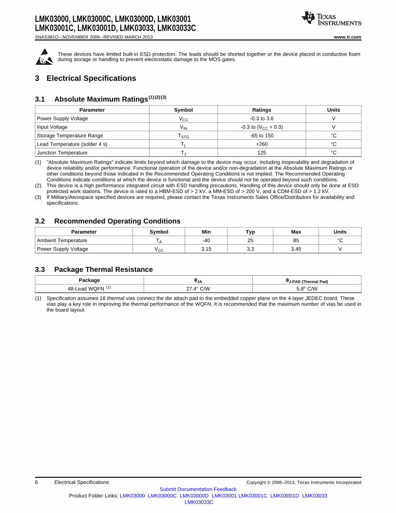
3 Electrical Specifications
3.1 Absolute Maximum Ratings (1) (2) (3)
Parameter Symbol Ratings Units
Power Supply Voltage VCC -0.3 to 3.6 V
Input Voltage VIN -0.3 to (VCC + 0.3) V
Storage Temperature Range TSTG -65 to 150 °C
Lead Temperature (solder 4 s) TL +260 °C
Junction Temperature TJ 125 °C
(1) "Absolute Maximum Ratings" indicate limits beyond which damage to the device may occur, including inoperability and degradation ofdevice reliability and/or performance. Functional operation of the device and/or non-degradation at the Absolute Maximum Ratings orother conditions beyond those indicated in the Recommended Operating Conditions is not implied. The Recommended OperatingConditions indicate conditions at which the device is functional and the device should not be operated beyond such conditions.
(2) This device is a high performance integrated circuit with ESD handling precautions. Handling of this device should only be done at ESDprotected work stations. The device is rated to a HBM-ESD of > 2 kV, a MM-ESD of > 200 V, and a CDM-ESD of > 1.2 kV.
(3) If Military/Aerospace specified devices are required, please contact the Texas Instruments Sales Office/Distributors for availability andspecifications.
3.2 Recommended Operating ConditionsParameter Symbol Min Typ Max Units
Ambient Temperature TA -40 25 85 °C
Power Supply Voltage VCC 3.15 3.3 3.45 V
3.3 Package Thermal ResistancePackage θJA θJ-PAD (Thermal Pad)
48-Lead WQFN (1) 27.4° C/W 5.8° C/W
(1) Specification assumes 16 thermal vias connect the die attach pad to the embedded copper plane on the 4-layer JEDEC board. Thesevias play a key role in improving the thermal performance of the WQFN. It is recommended that the maximum number of vias be used inthe board layout.
6 Electrical Specifications Copyright © 2006–2013, Texas Instruments Incorporated
Submit Documentation FeedbackProduct Folder Links: LMK03000 LMK03000C LMK03000D LMK03001 LMK03001C LMK03001D LMK03033
LMK03033C
LMK03000, LMK03000C, LMK03000D, LMK03001LMK03001C, LMK03001D, LMK03033, LMK03033C
www.ti.com SNAS381O –NOVEMBER 2006–REVISED MARCH 2013
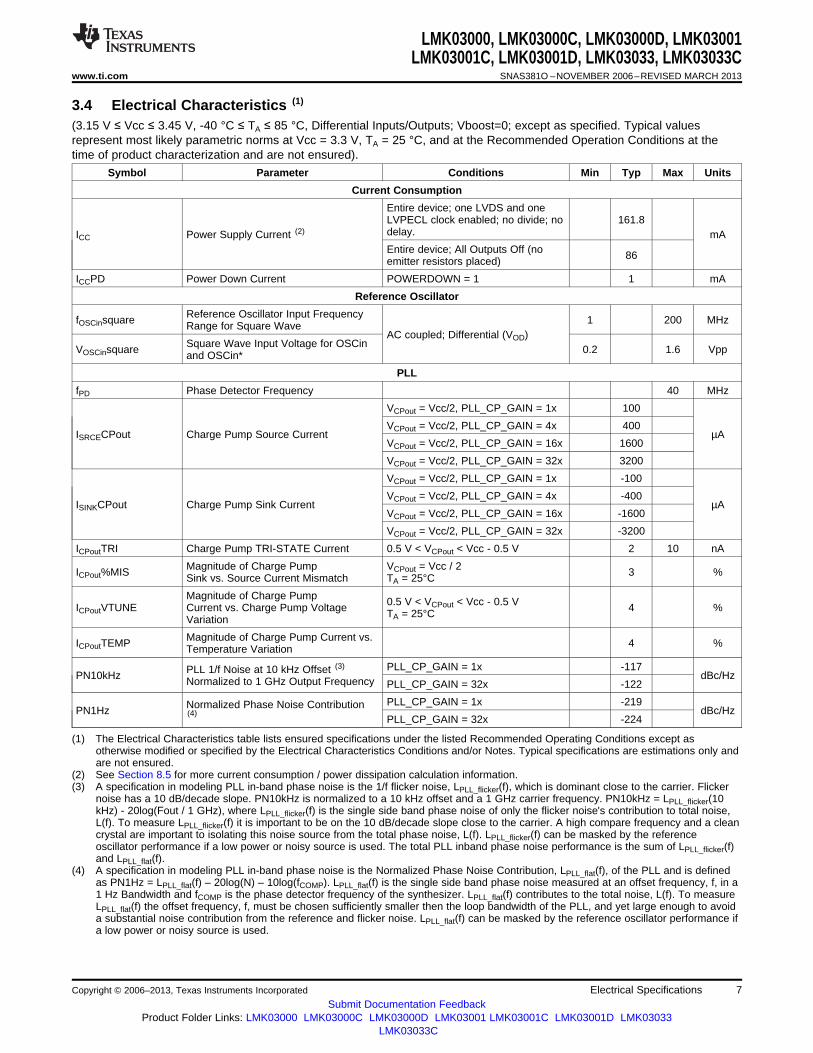
3.4 Electrical Characteristics (1)
(3.15 V ≤ Vcc ≤ 3.45 V, -40 °C ≤ TA ≤ 85 °C, Differential Inputs/Outputs; Vboost=0; except as specified. Typical valuesrepresent most likely parametric norms at Vcc = 3.3 V, TA = 25 °C, and at the Recommended Operation Conditions at thetime of product characterization and are not ensured).
Symbol Parameter Conditions Min Typ Max Units
Current Consumption
Entire device; one LVDS and oneLVPECL clock enabled; no divide; no 161.8delay.ICC Power Supply Current (2) mAEntire device; All Outputs Off (no 86emitter resistors placed)
ICCPD Power Down Current POWERDOWN = 1 1 mA
Reference Oscillator
Reference Oscillator Input FrequencyfOSCinsquare 1 200 MHzRange for Square WaveAC coupled; Differential (VOD)
Square Wave Input Voltage for OSCinVOSCinsquare 0.2 1.6 Vppand OSCin*
PLL
fPD Phase Detector Frequency 40 MHz
VCPout = Vcc/2, PLL_CP_GAIN = 1x 100
VCPout = Vcc/2, PLL_CP_GAIN = 4x 400ISRCECPout Charge Pump Source Current µA
VCPout = Vcc/2, PLL_CP_GAIN = 16x 1600
VCPout = Vcc/2, PLL_CP_GAIN = 32x 3200
VCPout = Vcc/2, PLL_CP_GAIN = 1x -100
VCPout = Vcc/2, PLL_CP_GAIN = 4x -400ISINKCPout Charge Pump Sink Current µA
VCPout = Vcc/2, PLL_CP_GAIN = 16x -1600
VCPout = Vcc/2, PLL_CP_GAIN = 32x -3200
ICPoutTRI Charge Pump TRI-STATE Current 0.5 V < VCPout < Vcc - 0.5 V 2 10 nA
Magnitude of Charge Pump VCPout = Vcc / 2ICPout%MIS 3 %Sink vs. Source Current Mismatch TA = 25°C
Magnitude of Charge Pump 0.5 V < VCPout < Vcc - 0.5 VICPoutVTUNE Current vs. Charge Pump Voltage 4 %TA = 25°CVariation
Magnitude of Charge Pump Current vs.ICPoutTEMP 4 %Temperature Variation
PLL_CP_GAIN = 1x -117PLL 1/f Noise at 10 kHz Offset (3)PN10kHz dBc/HzNormalized to 1 GHz Output Frequency PLL_CP_GAIN = 32x -122
PLL_CP_GAIN = 1x -219Normalized Phase Noise ContributionPN1Hz dBc/Hz(4)PLL_CP_GAIN = 32x -224
(1) The Electrical Characteristics table lists ensured specifications under the listed Recommended Operating Conditions except asotherwise modified or specified by the Electrical Characteristics Conditions and/or Notes. Typical specifications are estimations only andare not ensured.
(2) See Section 8.5 for more current consumption / power dissipation calculation information.(3) A specification in modeling PLL in-band phase noise is the 1/f flicker noise, LPLL_flicker(f), which is dominant close to the carrier. Flicker
noise has a 10 dB/decade slope. PN10kHz is normalized to a 10 kHz offset and a 1 GHz carrier frequency. PN10kHz = LPLL_flicker(10kHz) - 20log(Fout / 1 GHz), where LPLL_flicker(f) is the single side band phase noise of only the flicker noise's contribution to total noise,L(f). To measure LPLL_flicker(f) it is important to be on the 10 dB/decade slope close to the carrier. A high compare frequency and a cleancrystal are important to isolating this noise source from the total phase noise, L(f). LPLL_flicker(f) can be masked by the referenceoscillator performance if a low power or noisy source is used. The total PLL inband phase noise performance is the sum of LPLL_flicker(f)and LPLL_flat(f).
(4) A specification in modeling PLL in-band phase noise is the Normalized Phase Noise Contribution, LPLL_flat(f), of the PLL and is definedas PN1Hz = LPLL_flat(f) – 20log(N) – 10log(fCOMP). LPLL_flat(f) is the single side band phase noise measured at an offset frequency, f, in a1 Hz Bandwidth and fCOMP is the phase detector frequency of the synthesizer. LPLL_flat(f) contributes to the total noise, L(f). To measureLPLL_flat(f) the offset frequency, f, must be chosen sufficiently smaller then the loop bandwidth of the PLL, and yet large enough to avoida substantial noise contribution from the reference and flicker noise. LPLL_flat(f) can be masked by the reference oscillator performance ifa low power or noisy source is used.
Copyright © 2006–2013, Texas Instruments Incorporated Electrical Specifications 7Submit Documentation Feedback
Product Folder Links: LMK03000 LMK03000C LMK03000D LMK03001 LMK03001C LMK03001D LMK03033LMK03033C

LMK03000, LMK03000C, LMK03000D, LMK03001LMK03001C, LMK03001D, LMK03033, LMK03033CSNAS381O –NOVEMBER 2006–REVISED MARCH 2013 www.ti.com
Electrical Characteristics (1) (continued)
(3.15 V ≤ Vcc ≤ 3.45 V, -40 °C ≤ TA ≤ 85 °C, Differential Inputs/Outputs; Vboost=0; except as specified. Typical valuesrepresent most likely parametric norms at Vcc = 3.3 V, TA = 25 °C, and at the Recommended Operation Conditions at thetime of product characterization and are not ensured).
Symbol Parameter Conditions Min Typ Max Units
VCO
LMK03000C/LMK03000/LMK03000D 1185 1296
fFout VCO Tuning Range LMK03001C/LMK03001/LMK03001D 1470 1570 MHz
LMK03033C/LMK03033 1843 2160
After programming R15 for lock, noAllowable Temperature Drift for changes to output configuration are|ΔTCL| 125 °CContinuous Lock permitted to ensure continuous lock.
(1)
LMK03000C/LMK03000/LMK03000D; 3.3TA = 25 °COutput Power to a 50 Ω load driven bypFout LMK03001C/LMK03001/LMK03001D; dBmFout (2) 2.7TA = 25 °C
LMK03033C/LMK03033;TA = 25 °C -5 to 0
LMK03000C/LMK03000/LMK03000D 7 to 9
LMK03001C/LMK03001/LMK03001D 9 to 11KVCO Fine Tuning Sensitivity (3) MHz/V14 toLMK03033C/LMK03033 26
LMK03000C/LMK03001C 400
LMK03000/LMK03001 800Fout RMS Period JitterJRMSFout LMK03000D/LMK03001D 1200 fs(12 kHz to 20 MHz bandwidth)
LMK03033C 500
LMK03033 800
(1) Allowable Temperature Drift for Continuous Lock is how far the temperature can drift in either direction and stay in lock from the ambienttemperature and programmed state at which the device was when register R15 was programmed. The action of programming the R15register, even to the same value, activates a frequency calibration routine. This implies that the device will work over the entirefrequency range, but if the temperature drifts more than the maximum allowable drift for continuous lock, then it will be necessary toreprogram the R15 register to ensure that the device stays in lock. Regardless of what temperature the device was initially programmedat, the ambient temperature can never drift outside the range of -40 °C ≤ TA ≤ 85 °C without violating specifications. For thisspecification to be valid, the programmed state of the device must not change after R15 is programmed.
(2) Output power varies as a function of frequency. When a range is shown, the higher output power applies to the lower frequency and thelower output power applies to the higher frequency.
(3) The lower sensitivity indicates the typical sensitivity at the lower end of the tuning range, the higher sensitivity at the higher end of thetuning range
8 Electrical Specifications Copyright © 2006–2013, Texas Instruments Incorporated
Submit Documentation FeedbackProduct Folder Links: LMK03000 LMK03000C LMK03000D LMK03001 LMK03001C LMK03001D LMK03033
LMK03033C

LMK03000, LMK03000C, LMK03000D, LMK03001LMK03001C, LMK03001D, LMK03033, LMK03033C
www.ti.com SNAS381O –NOVEMBER 2006–REVISED MARCH 2013
Electrical Characteristics (1) (continued)
(3.15 V ≤ Vcc ≤ 3.45 V, -40 °C ≤ TA ≤ 85 °C, Differential Inputs/Outputs; Vboost=0; except as specified. Typical valuesrepresent most likely parametric norms at Vcc = 3.3 V, TA = 25 °C, and at the Recommended Operation Conditions at thetime of product characterization and are not ensured).
Symbol Parameter Conditions Min Typ Max Units
VCO (Continued)
10 kHz Offset -91.4
100 kHz Offset -116.8LMK03000CfFout = 1296 MHz (1)
1 MHz Offset -137.8
10 MHz Offset -156.9
10 kHz Offset -93.5
100 kHz Offset -118.5LMK03000CfFout = 1185 MHz (1)
1 MHz Offset -139.4
10 MHz Offset -158.4
10 kHz Offset -89.6
100 kHz Offset -115.2LMK03001CfFout = 1570 MHz (1)
1 MHz Offset -136.5
10 MHz Offset -156.0L(f)Fout Fout Single Side Band Phase Noise dBc/Hz
10 kHz Offset -91.6
100 kHz Offset -116.0LMK03001CfFout = 1470 MHz (1)
1 MHz Offset -137.9
10 MHz Offset -156.2
10 kHz Offset -83
100 kHz Offset -109LMK03033CfFout = 2160 MHz (1)
1 MHz Offset -131
10 MHz Offset -152
10 kHz Offset -86
100 kHz Offset -111LMK03033CfFout = 1843 MHz (1)
1 MHz Offset -134
10 MHz Offset -153
(1) VCO phase noise is measured assuming the VCO is the dominant noise source due to a 75 Hz loop bandwidth. Over frequency, thephase noise typically varies by 1 to 2 dB, with the worst case performance typically occurring at the highest frequency. Overtemperature, the phase noise typically varies by 1 to 2 dB, assuming the device is not reprogrammed. Reprogramming R15 will run thefrequency calibration routine for optimum phase noise.
Copyright © 2006–2013, Texas Instruments Incorporated Electrical Specifications 9Submit Documentation Feedback
Product Folder Links: LMK03000 LMK03000C LMK03000D LMK03001 LMK03001C LMK03001D LMK03033LMK03033C

LMK03000, LMK03000C, LMK03000D, LMK03001LMK03001C, LMK03001D, LMK03033, LMK03033CSNAS381O –NOVEMBER 2006–REVISED MARCH 2013 www.ti.com
Electrical Characteristics (1) (continued)
(3.15 V ≤ Vcc ≤ 3.45 V, -40 °C ≤ TA ≤ 85 °C, Differential Inputs/Outputs; Vboost=0; except as specified. Typical valuesrepresent most likely parametric norms at Vcc = 3.3 V, TA = 25 °C, and at the Recommended Operation Conditions at thetime of product characterization and are not ensured).
Symbol Parameter Conditions Min Typ Max Units
Clock Distribution Section (1) (2) - LVDS Clock Outputs
CLKoutX_MUX= Bypass (no 20
RL = 100 Ω divide or delay)Distribution Path =
CLKoutX_MUXJitterADD Additive RMS Jitter (1) 765 MHz fs= Divided (noBandwidth =delay) 7512 kHz to 20 MHzCLKoutX_DIV= 4
Equal loading and identical clocktSKEW CLKoutX to CLKoutY (3) configuration -30 ±4 30 ps
RL = 100 ΩVOD Differential Output Voltage RL = 100 Ω 250 350 450 mV
Change in magnitude of VOD forΔVOD RL = 100 Ω -50 50 mVcomplementary output states
VOS Output Offset Voltage RL = 100 Ω 1.070 1.25 1.370 V
Change in magnitude of VOS forΔVOS RL = 100 Ω -35 35 mVcomplementary output states
ISA Clock Output Short Circuit Current Single-ended outputs shorted to GND -24 24 mAISB single-ended
Clock Output Short Circuit CurrentISAB Complementary outputs tied together -12 12 mAdifferential
Clock Distribution Section (1) (2)- LVPECL Clock Outputs
CLKoutX_MUX= Bypass (no 20
RL = 100 Ω divide or delay)Distribution Path =
CLKoutX_MUXJitterADD Additive RMS Jitter (1) 765 MHz fs= Divided (noBandwidth =delay) 7512 kHz to 20 MHzCLKoutX_DIV= 4
Equal loading and identical clocktSKEW CLKoutX to CLKoutY (3) configuration -30 ±3 30 ps
Termination = 50 Ω to Vcc - 2 V
Vcc -VOH Output High Voltage V0.98Termination = 50 Ω to Vcc - 2 V
Vcc -VOL Output Low Voltage V1.8
VOD Differential Output Voltage RL = 100 Ω 660 810 965 mV
Digital LVTTL Interfaces (4)
VIH High-Level Input Voltage 2.0 Vcc V
VIL Low-Level Input Voltage 0.8 V
IIH High-Level Input Current VIH = Vcc -5.0 5.0 µA
IIL Low-Level Input Current VIL = 0 -40.0 5.0 µA
Vcc -VOH High-Level Output Voltage IOH = +500 µA V0.4
VOL Low-Level Output Voltage IOL = -500 µA 0.4 V
(1) The Clock Distribution Section includes all parts of the device except the PLL and VCO sections. Typical Additive Jitter specificationsapply to the clock distribution section only and this adds in an RMS fashion to the shaped jitter of the PLL and the VCO.
(2) For CLKout frequencies above 1 GHz, the delay should be limited to one half of a period. For 1 GHz and below, the maximum delay canbe used.
(3) Specification is ensured by characterization and is not tested in production.(4) Applies to GOE, LD, and SYNC*.
10 Electrical Specifications Copyright © 2006–2013, Texas Instruments Incorporated
Submit Documentation FeedbackProduct Folder Links: LMK03000 LMK03000C LMK03000D LMK03001 LMK03001C LMK03001D LMK03033
LMK03033C
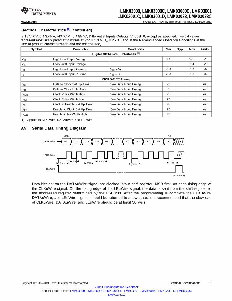
tCEStCS
D27 D26 D25 D24
tCHtCWH
tCWL
D23 D0 A3 A2 A1 A0
MSB LSB
DATAuWire
CLKuWire
LEuWire
tES
tEWH
LMK03000, LMK03000C, LMK03000D, LMK03001LMK03001C, LMK03001D, LMK03033, LMK03033C
www.ti.com SNAS381O –NOVEMBER 2006–REVISED MARCH 2013
Electrical Characteristics (1) (continued)
(3.15 V ≤ Vcc ≤ 3.45 V, -40 °C ≤ TA ≤ 85 °C, Differential Inputs/Outputs; Vboost=0; except as specified. Typical valuesrepresent most likely parametric norms at Vcc = 3.3 V, TA = 25 °C, and at the Recommended Operation Conditions at thetime of product characterization and are not ensured).
Symbol Parameter Conditions Min Typ Max Units
Digital MICROWIRE Interfaces (1)
VIH High-Level Input Voltage 1.6 Vcc V
VIL Low-Level Input Voltage 0.4 V
IIH High-Level Input Current VIH = Vcc -5.0 5.0 µA
IIL Low-Level Input Current VIL = 0 -5.0 5.0 µA
MICROWIRE Timing
tCS Data to Clock Set Up Time See Data Input Timing 25 ns
tCH Data to Clock Hold Time See Data Input Timing 8 ns
tCWH Clock Pulse Width High See Data Input Timing 25 ns
tCWL Clock Pulse Width Low See Data Input Timing 25 ns
tES Clock to Enable Set Up Time See Data Input Timing 25 ns
tCES Enable to Clock Set Up Time See Data Input Timing 25 ns
tEWH Enable Pulse Width High See Data Input Timing 25 ns
(1) Applies to CLKuWire, DATAuWire, and LEuWire.
3.5 Serial Data Timing Diagram
Data bits set on the DATAuWire signal are clocked into a shift register, MSB first, on each rising edge ofthe CLKuWire signal. On the rising edge of the LEuWire signal, the data is sent from the shift register tothe addressed register determined by the LSB bits. After the programming is complete the CLKuWire,DATAuWire, and LEuWire signals should be returned to a low state. It is recommended that the slew rateof CLKuWire, DATAuWire, and LEuWire should be at least 30 V/µs.
Copyright © 2006–2013, Texas Instruments Incorporated Electrical Specifications 11Submit Documentation Feedback
Product Folder Links: LMK03000 LMK03000C LMK03000D LMK03001 LMK03001C LMK03001D LMK03033LMK03033C

LMK03000, LMK03000C, LMK03000D, LMK03001LMK03001C, LMK03001D, LMK03033, LMK03033CSNAS381O –NOVEMBER 2006–REVISED MARCH 2013 www.ti.com
4 Measurement Definitions
4.1 Charge Pump Current Specification Definitions
I1 = Charge Pump Sink Current at VCPout = Vcc - ΔVI2 = Charge Pump Sink Current at VCPout = Vcc/2I3 = Charge Pump Sink Current at VCPout = ΔVI4 = Charge Pump Source Current at VCPout = Vcc - ΔVI5 = Charge Pump Source Current at VCPout = Vcc/2I6 = Charge Pump Source Current at VCPout = ΔVΔV = Voltage offset from the positive and negative supply rails. Defined to be 0.5 V for this device.
4.1.1 Charge Pump Output Current Magnitude Variation vs. Charge Pump Output Voltage
4.1.2 Charge Pump Sink Current vs. Charge Pump Output Source Current Mismatch
4.1.3 Charge Pump Output Current Magnitude Variation vs. Temperature
12 Measurement Definitions Copyright © 2006–2013, Texas Instruments Incorporated
Submit Documentation FeedbackProduct Folder Links: LMK03000 LMK03000C LMK03000D LMK03001 LMK03001C LMK03001D LMK03033
LMK03033C
0 2000
FREQUENCY (MHz)
-146
-148
-150
-152
-154
-156
-158
-160
Noi
se F
loor
(dB
c/H
z)
1200400 800 1600200 600 1000 1400 1800
Vboost = 1
Vboost = 0
0 2000
FREQUENCY (MHz)
-146
-148
-150
-152
-154
-156
-158
-160
Noi
se F
loor
(dB
c/H
z)
1200400 800 1600200 600 1000 1400 1800
Vboost = 1
Vboost = 0
0 2000
FREQUENCY (MHz)
1200400 800 1600200 600 1000 1400 1800
Vboost = 1
Vboost = 0
1000
900
700
600
400
200
100
0
800
500
300
VO
D (
mV
)
0 2000
FREQUENCY (MHz)
1200400 800 1600200 600 1000 1400 1800
Vboost = 1
Vboost = 0
1000
900
700
600
400
200
100
0
800
500
300
VO
D (
mV
)
LMK03000, LMK03000C, LMK03000D, LMK03001LMK03001C, LMK03001D, LMK03033, LMK03033C
www.ti.com SNAS381O –NOVEMBER 2006–REVISED MARCH 2013
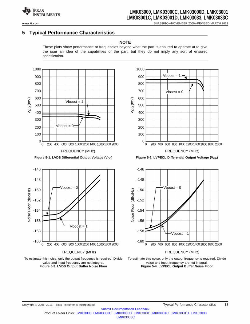
5 Typical Performance Characteristics
NOTEThese plots show performance at frequencies beyond what the part is ensured to operate at to givethe user an idea of the capabilities of the part, but they do not imply any sort of ensuredspecification.
Figure 5-1. LVDS Differential Output Voltage (VOD) Figure 5-2. LVPECL Differential Output Voltage (VOD)
To estimate this noise, only the output frequency is required. Divide To estimate this noise, only the output frequency is required. Dividevalue and input frequency are not integral. value and input frequency are not integral.
Figure 5-3. LVDS Output Buffer Noise Floor Figure 5-4. LVPECL Output Buffer Noise Floor
Copyright © 2006–2013, Texas Instruments Incorporated Typical Performance Characteristics 13Submit Documentation Feedback
Product Folder Links: LMK03000 LMK03000C LMK03000D LMK03001 LMK03001C LMK03001D LMK03033LMK03033C
10
-135
-140
-145
-150
-155
-160
-165
-170
NO
ISE
FLO
OR
(dB
c/H
z)
100 1000
FREQUENCY (MHz)
Delay = 2250 psDelay=1800 ps
Delay = 900 ps
Delay = 450 ps
Delay = 0 ps
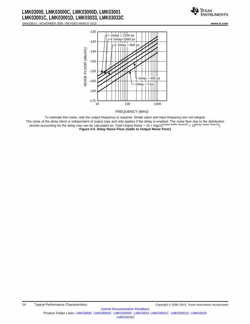
LMK03000, LMK03000C, LMK03000D, LMK03001LMK03001C, LMK03001D, LMK03033, LMK03033CSNAS381O –NOVEMBER 2006–REVISED MARCH 2013 www.ti.com
To estimate this noise, only the output frequency is required. Divide value and input frequency are not integral.The noise of the delay block is independent of output type and only applies if the delay is enabled. The noise floor due to the distribution
section accounting for the delay nise can be calculated as: Total Output Noise = 10 × log(10Output Buffer Noise/10 + 10Delay Noise Floor/10).Figure 5-5. Delay Noise Floor (Adds to Output Noise Floor)
14 Typical Performance Characteristics Copyright © 2006–2013, Texas Instruments Incorporated
Submit Documentation FeedbackProduct Folder Links: LMK03000 LMK03000C LMK03000D LMK03001 LMK03001C LMK03001D LMK03033
LMK03033C

LMK03000, LMK03000C, LMK03000D, LMK03001LMK03001C, LMK03001D, LMK03033, LMK03033C
www.ti.com SNAS381O –NOVEMBER 2006–REVISED MARCH 2013
6 Functional Description
The LMK03000 family of precision clock conditioners combine the functions of jittercleaning/reconditioning, multiplication, and distribution of a reference clock. The devices integrate aVoltage Controlled Oscillator (VCO), a high performance Integer-N Phase Locked Loop (PLL), a partiallyintegrated loop filter, three LVDS, and five LVPECL clock output distribution blocks.
The devices include internal 3rd and 4th order poles to simplify loop filter design and improve spuriousperformance. The 1st and 2nd order poles are off-chip to provide flexibility for the design of various loopfilter bandwidths.
The LMK03000 family has multiple options for VCO frequencies. The VCO output is optionally accessibleon the Fout port. Internally, the VCO output goes through an VCO Divider to feed the various clockdistribution blocks.
Each clock distribution block includes a programmable divider, a phase synchronization circuit, aprogrammable delay, a clock output mux, and an LVDS or LVPECL output buffer. This allows multipleinteger-related and phase-adjusted copies of the reference to be distributed to eight system components.
The clock conditioners come in a 48-pin WQFN package and are footprint compatible with other clockingdevices in the same family.
6.1 BIAS PIN
To properly use the device, bypass Bias (pin 36) with a low leakage 1 µF capacitor connected to Vcc. Thisis important for low noise performance.
6.2 LDO BYPASS
To properly use the device, bypass LDObyp1 (pin 9) with a 10 µF capacitor and LDObyp2 (pin 10) with a0.1 µF capacitor.
6.3 OSCILLATOR INPUT PORT (OSCin, OSCin*)
The purpose of OSCin is to provide the PLL with a reference signal. Due to an internal DC bias the OSCinport should be AC coupled, refer to the Section 8.1 in the Section 8 section. The OSCin port may bedriven single-endedly by AC grounding OSCin* with a 0.1 µF capacitor.
6.4 LOW NOISE, FULLY INTEGRATED VCO
The LMK03000 family of devices contain a fully integrated VCO. In order for proper operation the VCOuses a frequency calibration algorithm. The frequency calibration algorithm is activated any time that theR15 register is programmed. Once R15 is programmed the temperature may not drift more than themaximum allowable drift for continuous lock, ΔTCL, or else the VCO is not ensured to stay in lock.
For the frequency calibration algorithm to work properly OSCin must be driven by a valid signal when R15is programmed.
6.5 CLKout DELAYS
Each individual clock output includes a delay adjustment. Clock output delay registers (CLKoutX_DLY)support a 150 ps step size and range from 0 to 2250 ps of total delay.
Copyright © 2006–2013, Texas Instruments Incorporated Functional Description 15Submit Documentation Feedback
Product Folder Links: LMK03000 LMK03000C LMK03000D LMK03001 LMK03001C LMK03001D LMK03033LMK03033C

DistributionPath
SYNC*
CLKout0
CLKout1
CLKout2
LMK03000, LMK03000C, LMK03000D, LMK03001LMK03001C, LMK03001D, LMK03033, LMK03033CSNAS381O –NOVEMBER 2006–REVISED MARCH 2013 www.ti.com
6.6 LVDS/LVPECL OUTPUTS
By default all the clock outputs are disabled until programmed.
Each LVDS or LVPECL output may be disabled individually by programming the CLKoutX_EN bits. All theoutputs may be disabled simultaneously by pulling the GOE pin low or programming EN_CLKout_Globalto 0.
The duty cycle of the LVDS and LVPECL clock outputs are shown in the table below.VCO_DIV CLKoutX_MUX Duty Cycle
Any Divided, or Divided and Delayed 50%
2, 4, 6, 8 Any 50%
3 Bypassed, or Delayed 33%
5 Bypassed, or Delayed 40%
7 Bypassed, or Delayed 43%
6.7 GLOBAL CLOCK OUTPUT SYNCHRONIZATION
The SYNC* pin synchronizes the clock outputs. When the SYNC* pin is held in a logic low state, thedivided outputs are also held in a logic low state. The bypassed outputs will continue to operate normally.Shortly after the SYNC* pin goes high, the divided clock outputs are activated and will all transition to ahigh state simultaneously. All the outputs, divided and bypassed, will now be synchronized. Clocks in thebypassed state are not affected by SYNC* and are always synchronized with the divided outputs.
The SYNC* pin must be held low for greater than one clock cycle of the output of the VCO Divider, alsoknown as the distribution path. Once this low event has been registered, the outputs will not reflect the lowstate for four more cycles. This means that the outputs will be low on the fifth rising edge of thedistribution path. Similarly once the SYNC* pin becomes high, the outputs will not simultaneouslytransition high until four more distribution path clock cycles have passed, which is the fifth rising edge ofthe distribution path. See the timing diagram in Figure 6-1 for further detail. The clocks are programmedas CLKout0_MUX = Bypassed, CLKout1_MUX = Divided, CLKout1_DIV = 2, CLKout2_MUX = Divided,and CLKout2_DIV = 4. To synchronize the outputs, after the low SYNC* event has been registered, it isnot required to wait for the outputs to go low before SYNC* is set high.
Figure 6-1. SYNC* Timing Diagram
The SYNC* pin provides an internal pull-up resistor as shown on the functional block diagram. If theSYNC* pin is not terminated externally the clock outputs will operate normally. If the SYNC* function is notused, clock output synchronization is not ensured.
16 Functional Description Copyright © 2006–2013, Texas Instruments Incorporated
Submit Documentation FeedbackProduct Folder Links: LMK03000 LMK03000C LMK03000D LMK03001 LMK03001C LMK03001D LMK03033
LMK03033C

LMK03000, LMK03000C, LMK03000D, LMK03001LMK03001C, LMK03001D, LMK03033, LMK03033C
www.ti.com SNAS381O –NOVEMBER 2006–REVISED MARCH 2013
6.8 CLKout OUTPUT STATES
Each clock output may be individually enabled with the CLKoutX_EN bits. Each individual output enablecontrol bit is gated with the Global Output Enable input pin (GOE) and the Global Output Enable bit(EN_CLKout_Global).
All clock outputs can be disabled simultaneously if the GOE pin is pulled low by an external signal orEN_CLKout_Global is set to 0.CLKoutX_EN bit EN_CLKout_Global bit GOE pin CLKoutX Output State
1 1 Low Low
Don't care 0 Don't care Off
0 Don't care Don't care Off
1 1 High / No Connect Enabled
When an LVDS output is in the Off state, the outputs are at a voltage of approximately 1.5 volts. When anLVPECL output is in the Off state, the outputs are at a voltage of approximately 1 volt.
6.9 GLOBAL OUTPUT ENABLE AND LOCK DETECT
The GOE pin provides an internal pull-up resistor as shown on the functional block diagram. If it is notterminated externally, the clock output states are determined by the Clock Output Enable bits(CLKoutX_EN) and the EN_CLKout_Global bit.
By programming the PLL_MUX register to Digital Lock Detect Active High, the Lock Detect (LD) pin canbe connected to the GOE pin in which case all outputs are set low automatically if the synthesizer is notlocked.
6.10 POWER ON RESET
When supply voltage to the device increases monotonically from ground to Vcc, the power on reset circuitsets all registers to their default values, see the Section 7 section for more information on default registervalues. Voltage should be applied to all Vcc pins simultaneously.
Copyright © 2006–2013, Texas Instruments Incorporated Functional Description 17Submit Documentation Feedback
Product Folder Links: LMK03000 LMK03000C LMK03000D LMK03001 LMK03001C LMK03001D LMK03033LMK03033C

Phase Error < g
Phase Error < g Phase Error < g Phase Error < g Phase Error > *
YESNONONO
NONO
YES YES
YES YES YES
NO
Phase Error < gSTARTLock Detected =
False
Lock Detected =
True
LMK03000, LMK03000C, LMK03000D, LMK03001LMK03001C, LMK03001D, LMK03033, LMK03033CSNAS381O –NOVEMBER 2006–REVISED MARCH 2013 www.ti.com
6.11 DIGITAL LOCK DETECT
The PLL digital lock detect circuitry compares the difference between the phase of the inputs of the phasedetector to a RC generated delay of ε. To indicate a locked state the phase error must be less than the εRC delay for 5 consecutive reference cycles. Once in lock, the RC delay is changed to approximately δ.To indicate an out of lock state, the phase error must become greater δ. The values of ε and δ are shownin the table below:
ε δ10 ns 20 ns
To utilize the digital lock detect feature, PLL_MUX must be programmed for "Digital Lock Detect (ActiveHigh)" or "Digital Lock Detect (Active Low)." When one of these modes is programmed the state of the LDpin will be set high or low as determined by the description above as shown in Figure 6-2.
When the device is in power down mode and the LD pin is programmed for a digital lock detect function,LD will show a "no lock detected" condition which is low or high given active high or active low circuitryrespectively.
The accuracy of this circuit degrades at higher comparison frequencies. To compensate for this, the DIV4word should be set to one if the comparison frequency exceeds 20 MHz. The function of this word is todivide the comparison frequency presented to the lock detect circuit by 4.
Figure 6-2. Digital Lock Detect Flowchart
18 Functional Description Copyright © 2006–2013, Texas Instruments Incorporated
Submit Documentation FeedbackProduct Folder Links: LMK03000 LMK03000C LMK03000D LMK03001 LMK03001C LMK03001D LMK03033
LMK03033C

LMK03000, LMK03000C, LMK03000D, LMK03001LMK03001C, LMK03001D, LMK03033, LMK03033C
www.ti.com SNAS381O –NOVEMBER 2006–REVISED MARCH 2013
7 General Programming Information
The LMK03000 family of devices are programmed using several 32-bit registers which control the device'soperation. The registers consist of a data field and an address field. The last 4 register bits, ADDR[3:0]form the address field. The remaining 28 bits form the data field DATA[27:0].
During programming, LEuWire is low and serial data is clocked in on the rising edge of CLKuWire (MSBfirst). When LE goes high, data is transferred to the register bank selected by the address field. Onlyregisters R0 to R7, R11, and R13 to R15 need to be programmed for proper device operation.
For the frequency calibration algorithm to work properly OSCin must be driven by a valid signal when R15is programmed. Any changes to the PLL R divider or OSCin require R15 to be programmed again toactivate the frequency calibration routine.
7.1 RECOMMENDED PROGRAMMING SEQUENCE
The recommended programming sequence involves programming R0 with the reset bit set (RESET = 1) toensure the device is in a default state. It is not necessary to program R0 again, but if R0 is programmedagain, the reset bit is programmed clear (RESET = 0). Registers are programmed in order with R15 beingthe last register programmed. An example programming sequence is shown below.• Program R0 with the reset bit set (RESET = 1). This ensures the device is in a default state. When the
reset bit is set in R0, the other R0 bits are ignored.– If R0 is programmed again, the reset bit is programmed clear (RESET = 0).
• Program R0 to R7 as necessary with desired clocks with appropriate enable, mux, divider, and delaysettings.
• Program R8 for optimum phase noise performance.• Program R9 with Vboost setting if necessary. Optional, only needed to set Vboost = 1.• Program R11 with DIV4 setting if necessary.• Program R13 with oscillator input frequency and internal loop filter values• Program R14 with Fout enable bit, global clock output bit, power down setting, PLL mux setting, and
PLL R divider.• Program R15 with PLL charge pump gain, VCO divider, and PLL N divider. Also starts frequency
calibration routine.
Copyright © 2006–2013, Texas Instruments Incorporated General Programming Information 19Submit Documentation Feedback
Product Folder Links: LMK03000 LMK03000C LMK03000D LMK03001 LMK03001C LMK03001D LMK03033LMK03033C

LMK03000, LMK03000C, LMK03000D, LMK03001LMK03001C, LMK03001D, LMK03033, LMK03033CSNAS381O –NOVEMBER 2006–REVISED MARCH 2013 www.ti.com
Table 7-1. REGISTER MAP
31 30 29 28 27 26 25 24 23 22 21 20 19 18 17 16 15 14 13 12 11 10 9 8 7 6 5 4 3 2 1 0
Reg
iste
r
Data [27:0] A3 A2 A1 A0
CLKout0 CLKout0_DIV CLKout0_DLYR0 RESET 0 0 0 0 0 0 0 0 0 0 0 0 _MUX 0 0 0 0[7:0] [3:0][1:0]
CLK
out0
_EN
CLKout1 CLKout1_DIV CLKout1_DLYR1 0 0 0 0 0 0 0 0 0 0 0 0 0 _MUX 0 0 0 1[7:0] [3:0][1:0]
CLK
out1
_EN
CLKout2 CLKout2_DIV CLKout2_DLYR2 0 0 0 0 0 0 0 0 0 0 0 0 0 _MUX 0 0 1 0[7:0] [3:0][1:0]
CLK
out2
_EN
CLKout3 CLKout3_DIV CLKout3_DLYR3 0 0 0 0 0 0 0 0 0 0 0 0 0 _MUX 0 0 1 1[7:0] [3:0][1:0]
CLK
out3
_EN
CLKout4 CLKout4_DIV CLKout4_DLYR4 0 0 0 0 0 0 0 0 0 0 0 0 0 _MUX 0 1 0 0[7:0] [3:0][1:0]
CLK
out4
_EN
CLKout5 CLKout5_DIV CLKout5_DLYR5 0 0 0 0 0 0 0 0 0 0 0 0 0 _MUX 0 1 0 1[7:0] [3:0][1:0]
CLK
out5
_EN
CLKout6 CLKout6_DIV CLKout6_DLYR6 0 0 0 0 0 0 0 0 0 0 0 0 0 _MUX 0 1 1 0[7:0] [3:0][1:0]
CLK
out6
_EN
CLKout7 CLKout7_DIV CLKout7_DLYR7 0 0 0 0 0 0 0 0 0 0 0 0 0 _MUX 0 1 1 1[7:0] [3:0][1:0]
CLK
out7
_EN
R8 0 0 0 1 0 0 0 0 0 0 0 0 0 0 0 0 0 0 0 0 1 0 0 1 0 0 0 0 1 0 0 0
20 General Programming Information Copyright © 2006–2013, Texas Instruments Incorporated
Submit Documentation FeedbackProduct Folder Links: LMK03000 LMK03000C LMK03000D LMK03001 LMK03001C LMK03001D LMK03033
LMK03033C

LMK03000, LMK03000C, LMK03000D, LMK03001LMK03001C, LMK03001D, LMK03033, LMK03033C
www.ti.com SNAS381O –NOVEMBER 2006–REVISED MARCH 2013
Table 7-1. REGISTER MAP (continued)
31 30 29 28 27 26 25 24 23 22 21 20 19 18 17 16 15 14 13 12 11 10 9 8 7 6 5 4 3 2 1 0
Reg
iste
r
R9 1 0 1 0 0 0 0 0 0 0 0 0 0 0 1 0 0 1 0 1 0 1 0 0 0 0 0 1 0 0 1
Vbo
ost
R11 0 0 0 0 0 0 0 0 1 0 0 0 0 0 1 0 DIV4 0 0 0 0 0 0 0 0 0 0 0 1 0 1 1
VCO_ VCO_ VCO_OSCin_FREQR13 0 0 0 0 0 0 1 0 1 0 R4_LF R3_LF C3_C4_LF 1 1 0 1[7:0] [2:0] [2:0] [3:0]
PLL_MUX PLL_RR14 0 0 0 0 0 0 0 0 0 1 1 1 0[3:0] [11:0]
EN
_Fou
t
PO
WE
RD
OW
N
EN
_CLK
out_
Glo
bal
PLL_CP_ VCO_DIV PLL_NR15 0 0 0 0 1 1 1 1GAIN [3:0] [17:0][1:0]
Copyright © 2006–2013, Texas Instruments Incorporated General Programming Information 21Submit Documentation Feedback
Product Folder Links: LMK03000 LMK03000C LMK03000D LMK03001 LMK03001C LMK03001D LMK03033LMK03033C

LMK03000, LMK03000C, LMK03000D, LMK03001LMK03001C, LMK03001D, LMK03033, LMK03033CSNAS381O –NOVEMBER 2006–REVISED MARCH 2013 www.ti.com
7.2 REGISTER R0 to R7
Registers R0 through R7 control the eight clock outputs. Register R0 controls CLKout0, Register R1controls CLKout1, and so on. There is one additional bit in register R0 called RESET. Aside from this, thefunctions of these bits are identical. The X in CLKoutX_MUX, CLKoutX_DIV, CLKoutX_DLY, andCLKoutX_EN denote the actual clock output which may be from 0 to 7.
Table 7-2. Default Register Settings after Power on Reset
Default BitBit Name Bit State Bit Description RegisterBit Value Location
RESET 0 No reset, normal operation Reset to power on defaults R0 31
CLKoutX_MUX 0 Bypassed CLKoutX mux mode 18:17
CLKoutX_EN 0 Disabled CLKoutX enable 16R0 to R7
CLKoutX_DIV 1 Divide by 2 CLKoutX clock divide 15:8
CLKoutX_DLY 0 0 ps CLKoutX clock delay 7:4
Vboost 0 Normal Mode Output Power Control R9 16
DIV4 0 PDF ≤ 20 MHz Phase Detector Frequency R11 15
OSCin_FREQ 10 10 MHz OSCin OSCin Frequency in MHz 21:14
VCO_R4_LF 0 Low (~200 Ω) R4 internal loop filter values 13:11R13
VCO_R3_LF 0 Low (~600 Ω) R3 internal loop filter values 10:8
VCO_C3_C4_LF 0 C3 = 0 pF, C4 = 10 pF C3 and C4 internal loop filter values 7:4
EN_Fout 0 Fout disabled Fout enable 28
EN_CLKout_Global 1 Normal - CLKouts normal Global clock output enable 27
POWERDOWN 0 Normal - Device active Device power down R14 26
PLL_MUX 0 Disabled Multiplexer control for LD pin 23:20
PLL_R 10 R divider = 10 PLL R divide value 19:8
PLL_CP_GAIN 0 100 µA Charge pump current 31:30
VCO_DIV 2 Divide by 2 VCO divide value R15 29:26
PLL_N 760 N divider = 760 PLL N divide value 25:8
7.2.1 RESET bit -- R0 only
This bit is only in register R0. The use of this bit is optional and it should be set to '0' if not used. Settingthis bit to a '1' forces all registers to their power on reset condition and therefore automatically clears thisbit. If this bit is set, all other R0 bits are ignored and R0 needs to be programmed again if used with itsproper values and RESET = 0.
7.2.2 CLKoutX_MUX[1:0] -- Clock Output Multiplexers
These bits control the Clock Output Multiplexer for each clock output. Changing between the differentmodes changes the blocks in the signal path and therefore incurs a delay relative to the bypass mode.The different MUX modes and associated delays are listed below.
CLKoutX_MUX[1:0] Mode Added Delay Relative to Bypass Mode
0 Bypassed (default) 0 ps
1 Divided 100 ps
400 ps2 Delayed (In addition to the programmed delay)
500 ps3 Divided and Delayed (In addition to the programmed delay)
22 General Programming Information Copyright © 2006–2013, Texas Instruments Incorporated
Submit Documentation FeedbackProduct Folder Links: LMK03000 LMK03000C LMK03000D LMK03001 LMK03001C LMK03001D LMK03033
LMK03033C

LMK03000, LMK03000C, LMK03000D, LMK03001LMK03001C, LMK03001D, LMK03033, LMK03033C
www.ti.com SNAS381O –NOVEMBER 2006–REVISED MARCH 2013
7.2.3 CLKoutX_DIV[7:0] -- Clock Output Dividers
These bits control the clock output divider value. In order for these dividers to be active, the respectiveCLKoutX_MUX bit must be set to either "Divided" or "Divided and Delayed" mode. After all the dividers areprogramed, the SYNC* pin must be used to ensure that all edges of the clock outputs are aligned. TheClock Output Dividers follow the VCO Divider so the final clock divide for an output is VCO Divider × ClockOutput Divider. By adding the divider block to the output path a fixed delay of approximately 100 ps isincurred.
The actual Clock Output Divide value is twice the binary value programmed as listed in the table below.CLKoutX_DIV[7:0] Clock Output Divider value
0 0 0 0 0 0 0 0 Invalid
0 0 0 0 0 0 0 1 2 (default)
0 0 0 0 0 0 1 0 4
0 0 0 0 0 0 1 1 6
0 0 0 0 0 1 0 0 8
0 0 0 0 0 1 0 1 10
. . . . . . . . ...
1 1 1 1 1 1 1 1 510
7.2.4 CLKoutX_DLY[3:0] -- Clock Output Delays
These bits control the delay stages for each clock output. In order for these delays to be active, therespective CLKoutX_MUX (See Section 7.2.2) bit must be set to either "Delayed" or "Divided andDelayed" mode. By adding the delay block to the output path a fixed delay of approximately 400 ps isincurred in addition to the delay shown in the table below.
CLKoutX_DLY[3:0] Delay (ps)
0 0 (default)
1 150
2 300
3 450
4 600
5 750
6 900
7 1050
8 1200
9 1350
10 1500
11 1650
12 1800
13 1950
14 2100
15 2250
7.2.5 CLKoutX_EN bit -- Clock Output Enables
These bits control whether an individual clock output is enabled or not. If the EN_CLKout_Global bit (SeeSection 7.7.4) is set to zero or if GOE pin is held low, all CLKoutX_EN bit states will be ignored and allclock outputs will be disabled.
CLKoutX_EN bit Conditions CLKoutX State
0 EN_CLKout_Global bit = 1 Disabled (default)GOE pin = High / No Connect1 Enabled
Copyright © 2006–2013, Texas Instruments Incorporated General Programming Information 23Submit Documentation Feedback
Product Folder Links: LMK03000 LMK03000C LMK03000D LMK03001 LMK03001C LMK03001D LMK03033LMK03033C

LMK03000, LMK03000C, LMK03000D, LMK03001LMK03001C, LMK03001D, LMK03033, LMK03033CSNAS381O –NOVEMBER 2006–REVISED MARCH 2013 www.ti.com
7.3 REGISTER R8
The programming of register R8 provides optimum phase noise performance.
7.4 REGISTER R9
The programming of register R9 is optional. If it is not programmed the bit Vboost will be defaulted to 0,which is the test condition for all electrical characteristics.
7.4.1 Vboost -- Voltage Boost
By enabling this bit, the voltage output levels for all clock outputs is increased. Also, the noise floor isimproved
Vboost Typical LVDS Voltage Output (mV) Typical LVPECL Voltage Output (mV)
0 350 810
1 390 865
7.5 REGISTER R11
This register only has one bit and only needs to be programmed in the case that the phase detectorfrequency is greater than 20 MHz and digital lock detect is used. Otherwise, it is automatically defaulted tothe correct values.
7.5.1 DIV4 -- High Phase Detector Frequencies and Lock Detect
This bit divides the frequency presented to the digital lock detect circuitry by 4. It is necessary to get areliable output from the digital lock detect output in the case of a phase detector frequency frequencygreater than 20 MHz.
DIV4 Digital Lock Detect Circuitry Mode
Not divided0 Phase Detector Frequency ≤ 20 MHz (default)
Divided by 41 Phase Detector Frequency > 20 MHz
7.6 REGISTER R13
7.6.1 VCO_C3_C4_LF[3:0] -- Value for Internal Loop Filter Capacitors C3 and C4
These bits control the capacitor values for C3 and C4 in the internal loop filter.Loop Filter Capacitors
VCO_C3_C4_LF[3:0] C3 (pF) C4 (pF)
0 0 (default) 10 (default)
1 0 60
2 50 10
3 0 110
4 50 110
5 100 110
6 0 160
7 50 160
8 100 10
9 100 60
10 150 110
11 150 60
12 to 15 Invalid
24 General Programming Information Copyright © 2006–2013, Texas Instruments Incorporated
Submit Documentation FeedbackProduct Folder Links: LMK03000 LMK03000C LMK03000D LMK03001 LMK03001C LMK03001D LMK03033
LMK03033C

LMK03000, LMK03000C, LMK03000D, LMK03001LMK03001C, LMK03001D, LMK03033, LMK03033C
www.ti.com SNAS381O –NOVEMBER 2006–REVISED MARCH 2013
7.6.2 VCO_R3_LF[2:0] -- Value for Internal Loop Filter Resistor R3
These bits control the R3 resistor value in the internal loop filter. The recommended setting forVCO_R3_LF[2:0] = 0 for optimum phase noise and jitter.
VCO_R3_LF[2:0] R3 Value (kΩ)
0 Low (~600 Ω) (default)
1 10
2 20
3 30
4 40
5 to 7 Invalid
7.6.3 VCO_R4_LF[2:0] -- Value for Internal Loop Filter Resistor R4
These bits control the R4 resistor value in the internal loop filter. The recommended setting forVCO_R4_LF[2:0] = 0 for optimum phase noise and jitter.
VCO_R4_LF[2:0] R4 Value (kΩ)
0 Low (~200 Ω) (default)
1 10
2 20
3 30
4 40
5 to 7 Invalid
7.6.4 OSCin_FREQ[7:0] -- Oscillator Input Calibration Adjustment
These bits are to be programmed to the OSCin frequency. If the OSCin frequency is not an integralmultiple of 1 MHz, then round to the closest value.
OSCin_FREQ[7:0] OSCin Frequency
1 1 MHz
2 2 MHz
... ...
10 10 MHz (default)
... ...
200 200 MHz
201 to 255 Invalid
7.7 REGISTER R14
7.7.1 PLL_R[11:0] -- R Divider Value
These bits program the PLL R Divider and are programmed in binary fashion. Any changes to PLL_Rrequire R15 to be programmed again to active the frequency calibration routine.
PLL_R[11:0] PLL R Divide Value
0 0 0 0 0 0 0 0 0 0 0 0 Invalid
0 0 0 0 0 0 0 0 0 0 0 1 1
0 0 0 0 0 0 0 0 0 0 1 0 2
. . . . . . . . . . . . ...
0 0 0 0 0 0 0 0 1 0 1 0 10 (default)
. . . . . . . . . . . . ...
1 1 1 1 1 1 1 1 1 1 1 1 4095
Copyright © 2006–2013, Texas Instruments Incorporated General Programming Information 25Submit Documentation Feedback
Product Folder Links: LMK03000 LMK03000C LMK03000D LMK03001 LMK03001C LMK03001D LMK03033LMK03033C

LMK03000, LMK03000C, LMK03000D, LMK03001LMK03001C, LMK03001D, LMK03033, LMK03033CSNAS381O –NOVEMBER 2006–REVISED MARCH 2013 www.ti.com
7.7.2 PLL_MUX[3:0] -- Multiplexer Control for LD Pin
These bits set the output mode of the LD pin. The table below lists several different modes.PLL_MUX[3:0] Output Type LD Pin Function
0 Hi-Z Disabled (default)
1 Push-Pull Logic High
2 Push-Pull Logic Low
3 Push-Pull Digital Lock Detect (Active High)
4 Push-Pull Digital Lock Detect (Active Low)
5 Push-Pull Analog Lock Detect
Open Drain6 Analog Lock DetectNMOS
Open Drain7 Analog Lock DetectPMOS
8 Invalid
9 Push-Pull N Divider Output/2 (50% Duty Cycle)
10 Invalid
11 Push-Pull R Divider Output/2 (50% Duty Cycle)
12 to 15 Invalid
7.7.3 POWERDOWN bit -- Device Power Down
This bit can power down the device. Enabling this bit powers down the entire device and all blocks,regardless of the state of any of the other bits or pins.
POWERDOWN bit Mode
0 Normal Operation (default)
1 Entire Device Powered Down
7.7.4 EN_CLKout_Global bit -- Global Clock Output Enable
This bit overrides the individual CLKoutX_EN bits. When this bit is set to 0, all clock outputs are disabled,regardless of the state of any of the other bits or pins.
EN_CLKout_Global bit Clock Outputs
0 All Off
1 Normal Operation (default)
7.7.5 EN_Fout bit -- Fout port enable
This bit enables the Fout pin.EN_Fout bit Fout Pin Status
0 Disabled (default)
1 Enabled
26 General Programming Information Copyright © 2006–2013, Texas Instruments Incorporated
Submit Documentation FeedbackProduct Folder Links: LMK03000 LMK03000C LMK03000D LMK03001 LMK03001C LMK03001D LMK03033
LMK03033C

LMK03000, LMK03000C, LMK03000D, LMK03001LMK03001C, LMK03001D, LMK03033, LMK03033C
www.ti.com SNAS381O –NOVEMBER 2006–REVISED MARCH 2013
7.8 REGISTER R15
Programming R15 also activates the frequency calibration routine.
7.8.1 PLL_N[17:0] -- PLL N Divider
These bits program the divide value for the PLL N Divider. The PLL N Divider follows the VCO Divider andprecedes the PLL phase detector. Since the VCO Divider is also in the feedback path from the VCO to thePLL Phase Detector, the total N divide value, NTotal, is also influenced by the VCO Divider value. NTotal =PLL N Divider × VCO Divider. The VCO frequency is calculated as, fVCO = fOSCin × PLL N Divider × VCODivider / PLL R Divider. Since the PLL N divider is a pure binary counter there are no illegal divide valuesfor PLL_N[17:0] except for 0.
PLL_N[17:0] PLL N Divider Value
0 0 0 0 0 0 0 0 0 0 0 0 0 0 0 0 0 0 Invalid
0 0 0 0 0 0 0 0 0 0 0 0 0 0 0 0 0 1 1
. . . . . . . . . . . . . . . . . . ...
0 0 0 0 0 0 0 0 1 0 1 1 1 1 1 0 0 0 760 (default)
. . . . . . . . . . . . . . . . . . ...
1 1 1 1 1 1 1 1 1 1 1 1 1 1 1 1 1 1 262143
7.8.2 VCO_DIV[3:0] -- VCO Divider
These bits program the divide value for the VCO Divider. The VCO Divider follows the VCO output andprecedes the clock distribution blocks. Since the VCO Divider is in the feedback path from the VCO to thePLL phase detector the VCO Divider contributes to the total N divide value, NTotal. NTotal = PLL N Divider ×VCO Divider. The VCO Divider can not be bypassed. See Section 7.8.1 for more information on settingthe VCO frequency.
VCO_DIV[3:0] VCO Divider Value
0 0 0 0 Invalid
0 0 0 1 Invalid
0 0 1 0 2 (default)
0 0 1 1 3
0 1 0 0 4
0 1 0 1 5
0 1 1 0 6
0 1 1 1 7
1 0 0 0 8
1 0 0 1 Invalid
. . . . ...
1 1 1 1 Invalid
7.8.3 PLL_CP_GAIN[1:0] -- PLL Charge Pump Gain
These bits set the charge pump gain of the PLL.PLL_CP_GAIN[1:0] Charge Pump Gain
0 1x (default)
1 4x
2 16x
3 32x
Copyright © 2006–2013, Texas Instruments Incorporated General Programming Information 27Submit Documentation Feedback
Product Folder Links: LMK03000 LMK03000C LMK03000D LMK03001 LMK03001C LMK03001D LMK03033LMK03033C

CP
out
LEuWire
CLKuWire
DATAuWire
GOE
LD
(optional)
To Host
CLKout0
CLKout0*
CLKout1
CLKout1*
CLKout2
CLKout2*
CLKout3
CLKout3*
CLKout4
CLKout4*
CLKout5
CLKout5*
CLKout6
CLKout6*
CLKout7
CLKout7*
To SystemSYNC*
OSCin
OSCin*
Bia
s
Vcc
LDObyp1
LDObyp2
10 PF 0.1 PF
1 PF
0.1 PF
0.1 PF
LMK0300xx
100Ö
LMK03000, LMK03000C, LMK03000D, LMK03001LMK03001C, LMK03001D, LMK03033, LMK03033CSNAS381O –NOVEMBER 2006–REVISED MARCH 2013 www.ti.com
8 Application Information
8.1 SYSTEM LEVEL DIAGRAM
Figure 8-1. Typical Application
Figure 8-1 shows an LMK03000 family device used in a typical application. In this setup the clock may bemultiplied, reconditioned, and redistributed. Both the OSCin/OSCin* and CLKoutX/CLKoutX* pins can beused in a single-ended or a differential fashion, which is discussed later in this datasheet. The GOE pinneeds to be high for the outputs to operate. One technique sometimes used is to take the output of the LD(Lock Detect) pin and use this as an input to the GOE pin. If this is done, then the outputs will turn off iflock detect circuit detects that the PLL is out of lock. The loop filter actually consists of seven components,but four of these components that for the third and fourth poles of the loop filter are integrated in the chip.The first and second pole of the loop filter are external.
8.2 BIAS PIN
See Section 6.1 for bias pin information.
8.3 LDO BYPASS
See Section 6.2 for LDO bypass information.
28 Application Information Copyright © 2006–2013, Texas Instruments Incorporated
Submit Documentation FeedbackProduct Folder Links: LMK03000 LMK03000C LMK03000D LMK03001 LMK03001C LMK03001D LMK03033
LMK03033C

C2
Phase Detector
R2C1
C3 C4
R3 R4
LMK0300xx
Internal Loop Filter
External Loop Filter
LMK03000, LMK03000C, LMK03000D, LMK03001LMK03001C, LMK03001D, LMK03033, LMK03033C
www.ti.com SNAS381O –NOVEMBER 2006–REVISED MARCH 2013
8.4 LOOP FILTER
Figure 8-2. Loop Filter
The internal charge pump is directly connected to the integrated loop filter components. The first andsecond pole of the loop filter are externally attached as shown in Figure 8-2. When the loop filter isdesigned, it must be stable over the entire frequency band, meaning that the changes in KVtune from thelow to high band specification will not make the loop filter unstable. The design of the loop filter isapplication specific and can be rather involved, but is discussed in depth in the Clock Conditioner Owner'sManual provided by Texas Instruments. When designing with the integrated loop filter of the LMK03000family, considerations for minimum resistor thermal noise often lead one to the decision to design for theminimum value for integrated resistors, R3 and R4. Both the integrated loop filter resistors and capacitors(C3 and C4) also restrict how wide the loop bandwidth the PLL can have. However, these integratedcomponents do have the advantage that they are closer to the VCO and can therefore filter out somenoise and spurs better than external components. For this reason, a common strategy is to minimize theinternal loop filter resistors and then design for the largest internal capacitor values that permit a wideenough loop bandwidth. In some situations where spurs requirements are very stringent and there ismargin on phase noise, it might make sense to design for a loop filter with integrated resistor values thatare larger than their minimum value.
Copyright © 2006–2013, Texas Instruments Incorporated Application Information 29Submit Documentation Feedback
Product Folder Links: LMK03000 LMK03000C LMK03000D LMK03001 LMK03001C LMK03001D LMK03033LMK03033C

LMK03000, LMK03000C, LMK03000D, LMK03001LMK03001C, LMK03001D, LMK03033, LMK03033CSNAS381O –NOVEMBER 2006–REVISED MARCH 2013 www.ti.com
8.5 CURRENT CONSUMPTION / POWER DISSIPATION CALCULATIONS
Due to the myriad of possible configurations the following table serves to provide enough information toallow the user to calculate estimated current consumption of the device. Unless otherwise noted Vcc = 3.3V, TA = 25 °C.
Table 8-1. Block Current Consumption
PowerCurrent Power Dissipated inBlock Condition Consumption at Dissipated in LVPECL emitter3.3 V (mA) device (mW) resistors (mW)
Entire device, All outputs off; No LVPECL emitter resistors connected 86.0 283.8 -core current
Low clock buffer The low clock buffer is enabled anytime one of CLKout0 9 29.7 -(internal) through CLKout3 are enabled
High clock buffer The high clock buffer is enabled anytime one of the 9 29.7 -(internal) CLKout4 through CLKout7 are enabled
Fout buffer, EN_Fout = 1 14.5 47.8 -
LVDS output, Bypassed mode 17.8 58.7 -
LVPECL output, Bypassed mode (includes 120 Ω emitter 40 72 60resistors)Output buffersLVPECL output, disabled mode (includes 120 Ω emitter 17.4 38.3 19.1resistors)
LVPECL output, disabled mode. No emitter resistors 0 0 -placed; open outputs
Divide enabled, divide = 2 5.3 17.5 -Divide circuitryper output Divide enabled, divide > 2 8.5 28.0 -
Delay enabled, delay < 8 5.8 19.1 -Delay circuitry peroutput Delay enabled, delay > 7 9.9 32.7 -
Entire device CLKout0 & CLKout4 enabled in Bypassed mode 161.8 474 60
From Table 8-1 the current consumption can be calculated in any configuration. For example, the currentfor the entire device with 1 LVDS (CLKout0) & 1 LVPECL (CLKout4) output in Bypassed mode can becalculated by adding up the following blocks: core current, low clock buffer, high clock buffer, one LVDSoutput buffer current, and one LVPECL output buffer current. There will also be one LVPECL outputdrawing emitter current, but some of the power from the current draw is dissipated in the external 120 Ωresistors which doesn't add to the power dissipation budget for the device. If delays or divides areswitched in, then the additional current for these stages needs to be added as well.
For power dissipated by the device, the total current entering the device is multiplied by the voltage at thedevice minus the power dissipated in any emitter resistors connected to any of the LVPECL outputs. If noemitter resistors are connected to the LVPECL outputs, this power will be 0 watts. For example, in thecase of 1 LVDS (CLKout0) & 1 LVPECL (CLKout4) operating at 3.3 volts, we calculate 3.3 V × (86 + 9 + 9+ 17.8 + 40) mA = 3.3 V × 161.8 mA = 533.9 mW. Because the LVPECL output (CLKout4) has the emitterresistors hooked up and the power dissipated by these resistors is 60 mW, the total device powerdissipation is 533.9 mW - 60 mW = 473.9 mW.
When the LVPECL output is active, ~1.9 V is the average voltage on each output as calculated from theLVPECL Voh & Vol typical specification. Therefore the power dissipated in each emitter resistor isapproximately (1.9 V)2 / 120 Ω = 30 mW. When the LVPECL output is disabled, the emitter resistorvoltage is ~1.07 V. Therefore the power dissipated in each emitter resistor is approximately (1.07 V)2 / 120Ω = 9.5 mW.
30 Application Information Copyright © 2006–2013, Texas Instruments Incorporated
Submit Documentation FeedbackProduct Folder Links: LMK03000 LMK03000C LMK03000D LMK03001 LMK03001C LMK03001D LMK03033
LMK03033C

0.33 mm, typ
1.2 mm, typ
5.0 mm, min
LMK03000, LMK03000C, LMK03000D, LMK03001LMK03001C, LMK03001D, LMK03033, LMK03033C
www.ti.com SNAS381O –NOVEMBER 2006–REVISED MARCH 2013
8.6 THERMAL MANAGEMENT
Power consumption of the LMK03000 family of devices can be high enough to require attention to thermalmanagement. For reliability and performance reasons the die temperature should be limited to a maximumof 125 °C. That is, as an estimate, TA (ambient temperature) plus device power consumption times θJAshould not exceed 125 °C.
The package of the device has an exposed pad that provides the primary heat removal path as well asexcellent electrical grounding to the printed circuit board. To maximize the removal of heat from thepackage a thermal land pattern including multiple vias to a ground plane must be incorporated on the PCBwithin the footprint of the package. The exposed pad must be soldered down to ensure adequate heatconduction out of the package. A recommended land and via pattern is shown in Figure 8-3. Moreinformation on soldering WQFN packages can be obtained at www.ti.com.
Figure 8-3. Recommended Land and Via Pattern
To minimize junction temperature it is recommended that a simple heat sink be built into the PCB (if theground plane layer is not exposed). This is done by including a copper area of about 2 square inches onthe opposite side of the PCB from the device. This copper area may be plated or solder coated to preventcorrosion but should not have conformal coating (if possible), which could provide thermal insulation. Thevias shown in Figure 8-3 should connect these top and bottom copper layers and to the ground layer.These vias act as “heat pipes” to carry the thermal energy away from the device side of the board towhere it can be more effectively dissipated.
Copyright © 2006–2013, Texas Instruments Incorporated Application Information 31Submit Documentation Feedback
Product Folder Links: LMK03000 LMK03000C LMK03000D LMK03001 LMK03001C LMK03001D LMK03033LMK03033C

CLKoutX
CLKoutX*
LVDS Receiver10
0:100:Trace(Differential)
LVDSDriver
LMK03000, LMK03000C, LMK03000D, LMK03001LMK03001C, LMK03001D, LMK03033, LMK03033CSNAS381O –NOVEMBER 2006–REVISED MARCH 2013 www.ti.com
8.7 TERMINATION AND USE OF CLOCK OUTPUTS (DRIVERS)
When terminating clock drivers keep in mind these guidelines for optimum phase noise and jitterperformance:• Transmission line theory should be followed for good impedance matching to prevent reflections.• Clock drivers should be presented with the proper loads. For example:
– LVDS drivers are current drivers and require a closed current loop.– LVPECL drivers are open emitter and require a DC path to ground.
• Receivers should be presented with a signal biased to their specified DC bias level (common modevoltage) for proper operation. Some receivers have self-biasing inputs that automatically bias to theproper voltage level. In this case, the signal should normally be AC coupled.
It is possible to drive a non-LVPECL or non-LVDS receiver with a LVDS or LVPECL driver as long as theabove guidelines are followed. Check the datasheet of the receiver or input being driven to determine thebest termination and coupling method to be sure that the receiver is biased at its optimum DC voltage(common mode voltage). For example, when driving the OSCin/OSCin* input of the LMK03000 family,OSCin/OSCin* should be AC coupled because OSCin/OSCin* biases the signal to the proper DC level,see Figure 8-1. This is only slightly different from the AC coupled cases described in 3.7.2 because theDC blocking capacitors are placed between the termination and the OSCin/OSCin* pins, but the conceptremains the same, which is the receiver (OSCin/OSCin*) set the input to the optimum DC bias voltage(common mode voltage), not the driver.
8.7.1 Termination for DC Coupled Differential Operation
For DC coupled operation of an LVDS driver, terminate with 100 Ω as close as possible to the LVDSreceiver as shown in Figure 8-4. To ensure proper LVDS operation when DC coupling it is recommend touse LVDS receivers without fail-safe or internal input bias such as DS90LV110T. The LVDS driver willprovide the DC bias level for the LVDS receiver. For operation with LMK03000 family LVDS drivers it isrecommend to use AC coupling with LVDS receivers that have an internal DC bias voltage. Some fail-safecircuitry will present a DC bias (common mode voltage) which will prevent the LVDS driver from workingcorrectly. This precaution does not apply to the LVPECL drivers.
Figure 8-4. Differential LVDS Operation, DC Coupling
32 Application Information Copyright © 2006–2013, Texas Instruments Incorporated
Submit Documentation FeedbackProduct Folder Links: LMK03000 LMK03000C LMK03000D LMK03001 LMK03001C LMK03001D LMK03033
LMK03033C

CLKoutX
CLKoutX*
LVPECL Receiver
120:
100:Trace(Differential)
120:
Vcc
Vcc
LVPECL Driver
82:
82:
CLKoutX
CLKoutX*
LVPECL Receiver
50:
100:Trace(Differential)
50:
Vcc - 2 V
Vcc - 2 V
LVPECL Driver
LMK03000, LMK03000C, LMK03000D, LMK03001LMK03001C, LMK03001D, LMK03033, LMK03033C
www.ti.com SNAS381O –NOVEMBER 2006–REVISED MARCH 2013
For DC coupled operation of an LVPECL driver, terminate with 50 Ω to Vcc - 2 V as shown in Figure 8-5.Alternatively terminate with a Thevenin equivalent circuit (120 Ω resistor connected to Vcc and an 82 Ωresistor connected to ground with the driver connected to the junction of the 120 Ω and 82 Ω resistors) asshown in Figure 8-6 for Vcc = 3.3 V.
Figure 8-5. Differential LVPECL Operation, DC Coupling
Figure 8-6. Differential LVPECL Operation, DC Coupling, Thevenin Equivalent
Copyright © 2006–2013, Texas Instruments Incorporated Application Information 33Submit Documentation Feedback
Product Folder Links: LMK03000 LMK03000C LMK03000D LMK03001 LMK03001C LMK03001D LMK03033LMK03033C

CLKoutX
CLKoutX*
120:
120:
0.1 PF
0.1 PF
LVPECL Reciever
100:Trace(Differential)
LVPECLDriver
82:
120:
Vcc
82:
120:
Vcc
CLKoutX
CLKoutX*
0.1 PF
0.1 PF
LVDS Receiver
50:
100:Trace(Differential)
LVDSDriver
50:
Vbias
LMK03000, LMK03000C, LMK03000D, LMK03001LMK03001C, LMK03001D, LMK03033, LMK03033CSNAS381O –NOVEMBER 2006–REVISED MARCH 2013 www.ti.com
8.7.2 Termination for AC Coupled Differential Operation
AC coupling allows for shifting the DC bias level (common mode voltage) when driving different receiverstandards. Since AC coupling prevents the driver from providing a DC bias voltage at the receiver it isimportant to ensure the receiver is biased to its ideal DC level.
When driving LVDS receivers with an LVDS driver, the signal may be AC coupled by adding DC blockingcapacitors, however the proper DC bias point needs to be established at the receiver. If the receiver doesnot automatically bias its input, one way to do this is with the termination circuitry in Figure 8-7.
When using AC coupling with LVDS outputs, there may be a startup delay observed in the clock outputdue to capacitor charging. Figure 8-7 employs 0.1 µF capacitors. This value may need to be adjusted tomeet the startup requirements for a particular application.
Figure 8-7. Differential LVDS Operation, AC Coupling
LVPECL drivers require a DC path to ground. When AC coupling an LVPECL signal use 120 Ω emitterresistors close to the LVPECL driver to provide a DC path to ground as shown in Figure 8-8. For properreceiver operation, the signal should be biased to the DC bias level (common mode voltage) specified bythe receiver. The typical DC bias voltage (common mode voltage) for LVPECL receivers is 2 V. AThevenin equivalent circuit (82 Ω resistor connected to Vcc and a 120 Ω resistor connected to ground withthe driver connected to the junction of the 82 Ω and 120 Ω resistors) is a valid termination as shown inFigure 8-8 for Vcc = 3.3 V. Note this Thevenin circuit is different from the DC coupled example in Figure 8-6.
Figure 8-8. Differential LVPECL Operation, AC Coupling, Thevenin Equivalent
34 Application Information Copyright © 2006–2013, Texas Instruments Incorporated
Submit Documentation FeedbackProduct Folder Links: LMK03000 LMK03000C LMK03000D LMK03001 LMK03001C LMK03001D LMK03033
LMK03033C

CLKoutX
CLKoutX*
120:
120:
0.1 PF
0.1 PF
50:Trace
50:
Load50:
LVPECLDriver
CLKoutX
CLKoutX*
82:
50:Trace
120:
Load
Vcc
82:
120:
VccLVPECL
Driver
CLKoutX
CLKoutX* 50:
50:Trace
50:
Load
Vcc - 2V
Vcc - 2VLVPECL
Driver
LMK03000, LMK03000C, LMK03000D, LMK03001LMK03001C, LMK03001D, LMK03033, LMK03033C
www.ti.com SNAS381O –NOVEMBER 2006–REVISED MARCH 2013
8.7.3 Termination for Single-Ended Operation
A balun can be used with either LVDS or LVPECL drivers to convert the balanced, differential signal intoan unbalanced, single-ended signal.
It is possible to use an LVPECL driver as one or two separate 800 mV p-p signals. When DC coupling oneof the LMK03000 family clock LVPECL drivers, the termination should still be 50 ohms to Vcc - 2 V asshown in Figure 8-9. Again the Thevenin equivalent circuit (120 Ω resistor connected to Vcc and an 82 Ωresistor connected to ground with the driver connected to the junction of the 120 Ω and 82 Ω resistors) is avalid termination as shown in Figure 8-10 for Vcc = 3.3 V.
Figure 8-9. Single-Ended LVPECL Operation, DC Coupling
Figure 8-10. Single-Ended LVPECL Operation, DC Coupling, Thevenin Equivalent
When AC coupling an LVPECL driver use a 120 Ω emitter resistor to provide a DC path to ground andensure a 50 ohm termination with the proper DC bias level for the receiver. The typical DC bias voltage forLVPECL receivers is 2 V (See Section 8.7.2). If the other driver is not used it should be terminated witheither a proper AC or DC termination. This latter example of AC coupling a single-ended LVPECL signalcan be used to measure single-ended LVPECL performance using a spectrum analyzer or phase noiseanalyzer. When using most RF test equipment no DC bias (0 V DC) is expected for safe and properoperation. The internal 50 ohm termination the test equipment provides correctly terminates the LVPECLdriver being measured as shown Figure 8-11. When using only one LVPECL driver of aCLKoutX/CLKoutX* pair, be sure to properly terminate the unused driver.
Figure 8-11. Single-Ended LVPECL Operation, AC Coupling
Copyright © 2006–2013, Texas Instruments Incorporated Application Information 35Submit Documentation Feedback
Product Folder Links: LMK03000 LMK03000C LMK03000D LMK03001 LMK03001C LMK03001D LMK03033LMK03033C

10 70
FREQUENCY (MHz)
10
5
0
-5
-10
-15
-20
PO
WE
R (
dBm
)
50 80
Minimum Recommended Power for Differential
Operation
20 30 40 60 10090
Minimum Recommended Power for Single-Ended
Operation
0.1 PF
0.1 PF
LMKInput10
0:100:Trace(Differential)
Clock Source
0.1 PF
0.1 PF
50:Trace
50: LMK
InputClock Source
LMK03000, LMK03000C, LMK03000D, LMK03001LMK03001C, LMK03001D, LMK03033, LMK03033CSNAS381O –NOVEMBER 2006–REVISED MARCH 2013 www.ti.com
8.7.4 Conversion to LVCMOS Outputs
To drive an LVCMOS input with an LMK03000 family LVDS or LVPECL output, an LVPECL/LVDS toLVCMOS converter such as TI's DS90LV018A, DS90LV028A, DS90LV048A, etc. is required. For bestnoise performance, LVPECL provides a higher voltage swing into input of the converter.
8.8 OSCin INPUT
In addition to LVDS and LVPECL inputs, OSCin can also be driven with a sine wave. The OSCin input canbe driven single-ended or differentially with sine waves. The configurations for these are shown inFigure 8-12 and Figure 8-13. Figure 8-14 shows the recommended power level for sine wave operation forboth differential and single-ended sources over frequency. The part will operate at power levels below therecommended power level, but as power decreases the PLL noise performance will degrade. The VCOnoise performance will remain constant. At the recommended power level the PLL phase noisedegradation from full power operation (8 dBm) is less than 2 dB.
Figure 8-12. Single-Ended Sine Wave Input
Figure 8-13. Differential Sine Wave Input
Figure 8-14. Recommended OSCin Power for Operation with a Sine Wave Input
36 Application Information Copyright © 2006–2013, Texas Instruments Incorporated
Submit Documentation FeedbackProduct Folder Links: LMK03000 LMK03000C LMK03000D LMK03001 LMK03001C LMK03001D LMK03033
LMK03033C

LMK03000, LMK03000C, LMK03000D, LMK03001LMK03001C, LMK03001D, LMK03033, LMK03033C
www.ti.com SNAS381O –NOVEMBER 2006–REVISED MARCH 2013
8.9 MORE THAN EIGHT OUTPUTS WITH AN LMK03000 FAMILY DEVICE
The LMK03000 family devices include eight or less outputs. When more than 8 outputs are required thefootprint compatible LMK01000 family may be used for clock distribution. By using an LMK03000 devicewith eight LMK01000 family devices up to 64 clocks may be distributed in many different LVDS / LVPECLcombinations. It's possible to distribute more than 64 clocks by adding more LMK01000 family devices.Refer to AN-1864 (literature number SNAA060) for more details on how to do this.
Copyright © 2006–2013, Texas Instruments Incorporated Application Information 37Submit Documentation Feedback
Product Folder Links: LMK03000 LMK03000C LMK03000D LMK03001 LMK03001C LMK03001D LMK03033LMK03033C

LMK03000, LMK03000C, LMK03000D, LMK03001LMK03001C, LMK03001D, LMK03033, LMK03033CSNAS381O –NOVEMBER 2006–REVISED MARCH 2013 www.ti.com
Revision HistoryNOTE: Page numbers for previous revisions may differ from page numbers in the current version.
Changes from Revision N (March 2013) to Revision O Page
• Changed layout of National Data Sheet to TI format .......................................................................... 37
38 Application Information Copyright © 2006–2013, Texas Instruments Incorporated
Submit Documentation FeedbackProduct Folder Links: LMK03000 LMK03000C LMK03000D LMK03001 LMK03001C LMK03001D LMK03033
LMK03033C

PACKAGE OPTION ADDENDUM
www.ti.com 11-Apr-2013
Addendum-Page 1
PACKAGING INFORMATION
Orderable Device Status(1)
Package Type PackageDrawing
Pins PackageQty
Eco Plan(2)
Lead/Ball Finish MSL Peak Temp(3)
Op Temp (°C) Top-Side Markings(4)
Samples
LMK03000CISQ/NOPB ACTIVE WQFN RHS 48 250 Green (RoHS& no Sb/Br)
CU SN Level-3-260C-168 HR -40 to 85 K03000CI
LMK03000CISQX/NOPB ACTIVE WQFN RHS 48 2500 Green (RoHS& no Sb/Br)
CU SN Level-3-260C-168 HR -40 to 85 K03000CI
LMK03000DISQ/NOPB ACTIVE WQFN RHS 48 1000 Green (RoHS& no Sb/Br)
CU SN Level-3-260C-168 HR -40 to 85 K03000DI
LMK03000DISQE/NOPB ACTIVE WQFN RHS 48 250 Green (RoHS& no Sb/Br)
CU SN Level-3-260C-168 HR -40 to 85 K03000DI
LMK03000DISQX/NOPB ACTIVE WQFN RHS 48 2500 Green (RoHS& no Sb/Br)
CU SN Level-3-260C-168 HR -40 to 85 K03000DI
LMK03000ISQ/NOPB ACTIVE WQFN RHS 48 250 Green (RoHS& no Sb/Br)
CU SN Level-3-260C-168 HR -40 to 85 K03000 I
LMK03000ISQX/NOPB ACTIVE WQFN RHS 48 2500 Green (RoHS& no Sb/Br)
CU SN Level-3-260C-168 HR -40 to 85 K03000 I
LMK03001CISQ/NOPB ACTIVE WQFN RHS 48 250 Green (RoHS& no Sb/Br)
CU SN Level-3-260C-168 HR -40 to 85 K03001CI
LMK03001CISQX/NOPB ACTIVE WQFN RHS 48 2500 Green (RoHS& no Sb/Br)
CU SN Level-3-260C-168 HR -40 to 85 K03001CI
LMK03001DISQ/NOPB ACTIVE WQFN RHS 48 1000 Green (RoHS& no Sb/Br)
CU SN Level-3-260C-168 HR -40 to 85 K03001DI
LMK03001DISQE/NOPB ACTIVE WQFN RHS 48 250 Green (RoHS& no Sb/Br)
CU SN Level-3-260C-168 HR -40 to 85 K03001DI
LMK03001DISQX/NOPB ACTIVE WQFN RHS 48 2500 Green (RoHS& no Sb/Br)
CU SN Level-3-260C-168 HR -40 to 85 K03001DI
LMK03001ISQ/NOPB ACTIVE WQFN RHS 48 250 Green (RoHS& no Sb/Br)
CU SN Level-3-260C-168 HR -40 to 85 K03001 I
LMK03001ISQX/NOPB ACTIVE WQFN RHS 48 2500 Green (RoHS& no Sb/Br)
CU SN Level-3-260C-168 HR -40 to 85 K03001 I
LMK03033CISQ/NOPB ACTIVE WQFN RHS 48 1000 Green (RoHS& no Sb/Br)
CU SN Level-3-260C-168 HR -40 to 85 K03033CI
LMK03033CISQE/NOPB ACTIVE WQFN RHS 48 250 Green (RoHS& no Sb/Br)
CU SN Level-3-260C-168 HR -40 to 85 K03033CI
LMK03033CISQX/NOPB ACTIVE WQFN RHS 48 2500 Green (RoHS& no Sb/Br)
CU SN Level-3-260C-168 HR -40 to 85 K03033CI

PACKAGE OPTION ADDENDUM
www.ti.com 11-Apr-2013
Addendum-Page 2
Orderable Device Status(1)
Package Type PackageDrawing
Pins PackageQty
Eco Plan(2)
Lead/Ball Finish MSL Peak Temp(3)
Op Temp (°C) Top-Side Markings(4)
Samples
LMK03033ISQ/NOPB ACTIVE WQFN RHS 48 1000 Green (RoHS& no Sb/Br)
CU SN Level-3-260C-168 HR -40 to 85 K03033 I
LMK03033ISQE/NOPB ACTIVE WQFN RHS 48 250 Green (RoHS& no Sb/Br)
CU SN Level-3-260C-168 HR -40 to 85 K03033 I
LMK03033ISQX/NOPB ACTIVE WQFN RHS 48 2500 Green (RoHS& no Sb/Br)
CU SN Level-3-260C-168 HR -40 to 85 K03033 I
(1) The marketing status values are defined as follows:ACTIVE: Product device recommended for new designs.LIFEBUY: TI has announced that the device will be discontinued, and a lifetime-buy period is in effect.NRND: Not recommended for new designs. Device is in production to support existing customers, but TI does not recommend using this part in a new design.PREVIEW: Device has been announced but is not in production. Samples may or may not be available.OBSOLETE: TI has discontinued the production of the device.
(2) Eco Plan - The planned eco-friendly classification: Pb-Free (RoHS), Pb-Free (RoHS Exempt), or Green (RoHS & no Sb/Br) - please check http://www.ti.com/productcontent for the latest availabilityinformation and additional product content details.TBD: The Pb-Free/Green conversion plan has not been defined.Pb-Free (RoHS): TI's terms "Lead-Free" or "Pb-Free" mean semiconductor products that are compatible with the current RoHS requirements for all 6 substances, including the requirement thatlead not exceed 0.1% by weight in homogeneous materials. Where designed to be soldered at high temperatures, TI Pb-Free products are suitable for use in specified lead-free processes.Pb-Free (RoHS Exempt): This component has a RoHS exemption for either 1) lead-based flip-chip solder bumps used between the die and package, or 2) lead-based die adhesive used betweenthe die and leadframe. The component is otherwise considered Pb-Free (RoHS compatible) as defined above.Green (RoHS & no Sb/Br): TI defines "Green" to mean Pb-Free (RoHS compatible), and free of Bromine (Br) and Antimony (Sb) based flame retardants (Br or Sb do not exceed 0.1% by weightin homogeneous material)
(3) MSL, Peak Temp. -- The Moisture Sensitivity Level rating according to the JEDEC industry standard classifications, and peak solder temperature.
(4) Multiple Top-Side Markings will be inside parentheses. Only one Top-Side Marking contained in parentheses and separated by a "~" will appear on a device. If a line is indented then it is acontinuation of the previous line and the two combined represent the entire Top-Side Marking for that device.
Important Information and Disclaimer:The information provided on this page represents TI's knowledge and belief as of the date that it is provided. TI bases its knowledge and belief on informationprovided by third parties, and makes no representation or warranty as to the accuracy of such information. Efforts are underway to better integrate information from third parties. TI has taken andcontinues to take reasonable steps to provide representative and accurate information but may not have conducted destructive testing or chemical analysis on incoming materials and chemicals.TI and TI suppliers consider certain information to be proprietary, and thus CAS numbers and other limited information may not be available for release.
In no event shall TI's liability arising out of such information exceed the total purchase price of the TI part(s) at issue in this document sold by TI to Customer on an annual basis.

TAPE AND REEL INFORMATION
*All dimensions are nominal
Device PackageType
PackageDrawing
Pins SPQ ReelDiameter
(mm)
ReelWidth
W1 (mm)
A0(mm)
B0(mm)
K0(mm)
P1(mm)
W(mm)
Pin1Quadrant
LMK03000CISQ/NOPB WQFN RHS 48 250 178.0 16.4 7.3 7.3 1.3 12.0 16.0 Q1
LMK03000CISQX/NOPB WQFN RHS 48 2500 330.0 16.4 7.3 7.3 1.3 12.0 16.0 Q1
LMK03000DISQ/NOPB WQFN RHS 48 1000 330.0 16.4 7.3 7.3 1.3 12.0 16.0 Q1
LMK03000DISQE/NOPB WQFN RHS 48 250 178.0 16.4 7.3 7.3 1.3 12.0 16.0 Q1
LMK03000DISQX/NOPB WQFN RHS 48 2500 330.0 16.4 7.3 7.3 1.3 12.0 16.0 Q1
LMK03000ISQ/NOPB WQFN RHS 48 250 178.0 16.4 7.3 7.3 1.3 12.0 16.0 Q1
LMK03000ISQX/NOPB WQFN RHS 48 2500 330.0 16.4 7.3 7.3 1.3 12.0 16.0 Q1
LMK03001CISQ/NOPB WQFN RHS 48 250 178.0 16.4 7.3 7.3 1.3 12.0 16.0 Q1
LMK03001CISQX/NOPB WQFN RHS 48 2500 330.0 16.4 7.3 7.3 1.3 12.0 16.0 Q1
LMK03001DISQ/NOPB WQFN RHS 48 1000 330.0 16.4 7.3 7.3 1.3 12.0 16.0 Q1
LMK03001DISQE/NOPB WQFN RHS 48 250 178.0 16.4 7.3 7.3 1.3 12.0 16.0 Q1
LMK03001DISQX/NOPB WQFN RHS 48 2500 330.0 16.4 7.3 7.3 1.3 12.0 16.0 Q1
LMK03001ISQ/NOPB WQFN RHS 48 250 178.0 16.4 7.3 7.3 1.3 12.0 16.0 Q1
LMK03001ISQX/NOPB WQFN RHS 48 2500 330.0 16.4 7.3 7.3 1.3 12.0 16.0 Q1
LMK03033CISQ/NOPB WQFN RHS 48 1000 330.0 16.4 7.3 7.3 1.3 12.0 16.0 Q1
LMK03033CISQE/NOPB WQFN RHS 48 250 178.0 16.4 7.3 7.3 1.3 12.0 16.0 Q1
LMK03033CISQX/NOPB WQFN RHS 48 2500 330.0 16.4 7.3 7.3 1.3 12.0 16.0 Q1
LMK03033ISQ/NOPB WQFN RHS 48 1000 330.0 16.4 7.3 7.3 1.3 12.0 16.0 Q1
PACKAGE MATERIALS INFORMATION
www.ti.com 10-Jan-2018
Pack Materials-Page 1

Device PackageType
PackageDrawing
Pins SPQ ReelDiameter
(mm)
ReelWidth
W1 (mm)
A0(mm)
B0(mm)
K0(mm)
P1(mm)
W(mm)
Pin1Quadrant
LMK03033ISQE/NOPB WQFN RHS 48 250 178.0 16.4 7.3 7.3 1.3 12.0 16.0 Q1
LMK03033ISQX/NOPB WQFN RHS 48 2500 330.0 16.4 7.3 7.3 1.3 12.0 16.0 Q1
*All dimensions are nominal
Device Package Type Package Drawing Pins SPQ Length (mm) Width (mm) Height (mm)
LMK03000CISQ/NOPB WQFN RHS 48 250 210.0 185.0 35.0
LMK03000CISQX/NOPB WQFN RHS 48 2500 367.0 367.0 38.0
LMK03000DISQ/NOPB WQFN RHS 48 1000 367.0 367.0 38.0
LMK03000DISQE/NOPB WQFN RHS 48 250 210.0 185.0 35.0
LMK03000DISQX/NOPB WQFN RHS 48 2500 367.0 367.0 38.0
LMK03000ISQ/NOPB WQFN RHS 48 250 210.0 185.0 35.0
LMK03000ISQX/NOPB WQFN RHS 48 2500 367.0 367.0 38.0
LMK03001CISQ/NOPB WQFN RHS 48 250 210.0 185.0 35.0
LMK03001CISQX/NOPB WQFN RHS 48 2500 367.0 367.0 38.0
LMK03001DISQ/NOPB WQFN RHS 48 1000 367.0 367.0 38.0
LMK03001DISQE/NOPB WQFN RHS 48 250 210.0 185.0 35.0
LMK03001DISQX/NOPB WQFN RHS 48 2500 367.0 367.0 38.0
LMK03001ISQ/NOPB WQFN RHS 48 250 210.0 185.0 35.0
LMK03001ISQX/NOPB WQFN RHS 48 2500 367.0 367.0 38.0
LMK03033CISQ/NOPB WQFN RHS 48 1000 367.0 367.0 38.0
PACKAGE MATERIALS INFORMATION
www.ti.com 10-Jan-2018
Pack Materials-Page 2

Device Package Type Package Drawing Pins SPQ Length (mm) Width (mm) Height (mm)
LMK03033CISQE/NOPB WQFN RHS 48 250 210.0 185.0 35.0
LMK03033CISQX/NOPB WQFN RHS 48 2500 367.0 367.0 38.0
LMK03033ISQ/NOPB WQFN RHS 48 1000 367.0 367.0 38.0
LMK03033ISQE/NOPB WQFN RHS 48 250 210.0 185.0 35.0
LMK03033ISQX/NOPB WQFN RHS 48 2500 367.0 367.0 38.0
PACKAGE MATERIALS INFORMATION
www.ti.com 10-Jan-2018
Pack Materials-Page 3

IMPORTANT NOTICE
Texas Instruments Incorporated (TI) reserves the right to make corrections, enhancements, improvements and other changes to itssemiconductor products and services per JESD46, latest issue, and to discontinue any product or service per JESD48, latest issue. Buyersshould obtain the latest relevant information before placing orders and should verify that such information is current and complete.TI’s published terms of sale for semiconductor products (http://www.ti.com/sc/docs/stdterms.htm) apply to the sale of packaged integratedcircuit products that TI has qualified and released to market. Additional terms may apply to the use or sale of other types of TI products andservices.Reproduction of significant portions of TI information in TI data sheets is permissible only if reproduction is without alteration and isaccompanied by all associated warranties, conditions, limitations, and notices. TI is not responsible or liable for such reproduceddocumentation. Information of third parties may be subject to additional restrictions. Resale of TI products or services with statementsdifferent from or beyond the parameters stated by TI for that product or service voids all express and any implied warranties for theassociated TI product or service and is an unfair and deceptive business practice. TI is not responsible or liable for any such statements.Buyers and others who are developing systems that incorporate TI products (collectively, “Designers”) understand and agree that Designersremain responsible for using their independent analysis, evaluation and judgment in designing their applications and that Designers havefull and exclusive responsibility to assure the safety of Designers' applications and compliance of their applications (and of all TI productsused in or for Designers’ applications) with all applicable regulations, laws and other applicable requirements. Designer represents that, withrespect to their applications, Designer has all the necessary expertise to create and implement safeguards that (1) anticipate dangerousconsequences of failures, (2) monitor failures and their consequences, and (3) lessen the likelihood of failures that might cause harm andtake appropriate actions. Designer agrees that prior to using or distributing any applications that include TI products, Designer willthoroughly test such applications and the functionality of such TI products as used in such applications.TI’s provision of technical, application or other design advice, quality characterization, reliability data or other services or information,including, but not limited to, reference designs and materials relating to evaluation modules, (collectively, “TI Resources”) are intended toassist designers who are developing applications that incorporate TI products; by downloading, accessing or using TI Resources in anyway, Designer (individually or, if Designer is acting on behalf of a company, Designer’s company) agrees to use any particular TI Resourcesolely for this purpose and subject to the terms of this Notice.TI’s provision of TI Resources does not expand or otherwise alter TI’s applicable published warranties or warranty disclaimers for TIproducts, and no additional obligations or liabilities arise from TI providing such TI Resources. TI reserves the right to make corrections,enhancements, improvements and other changes to its TI Resources. TI has not conducted any testing other than that specificallydescribed in the published documentation for a particular TI Resource.Designer is authorized to use, copy and modify any individual TI Resource only in connection with the development of applications thatinclude the TI product(s) identified in such TI Resource. NO OTHER LICENSE, EXPRESS OR IMPLIED, BY ESTOPPEL OR OTHERWISETO ANY OTHER TI INTELLECTUAL PROPERTY RIGHT, AND NO LICENSE TO ANY TECHNOLOGY OR INTELLECTUAL PROPERTYRIGHT OF TI OR ANY THIRD PARTY IS GRANTED HEREIN, including but not limited to any patent right, copyright, mask work right, orother intellectual property right relating to any combination, machine, or process in which TI products or services are used. Informationregarding or referencing third-party products or services does not constitute a license to use such products or services, or a warranty orendorsement thereof. Use of TI Resources may require a license from a third party under the patents or other intellectual property of thethird party, or a license from TI under the patents or other intellectual property of TI.TI RESOURCES ARE PROVIDED “AS IS” AND WITH ALL FAULTS. TI DISCLAIMS ALL OTHER WARRANTIES ORREPRESENTATIONS, EXPRESS OR IMPLIED, REGARDING RESOURCES OR USE THEREOF, INCLUDING BUT NOT LIMITED TOACCURACY OR COMPLETENESS, TITLE, ANY EPIDEMIC FAILURE WARRANTY AND ANY IMPLIED WARRANTIES OFMERCHANTABILITY, FITNESS FOR A PARTICULAR PURPOSE, AND NON-INFRINGEMENT OF ANY THIRD PARTY INTELLECTUALPROPERTY RIGHTS. TI SHALL NOT BE LIABLE FOR AND SHALL NOT DEFEND OR INDEMNIFY DESIGNER AGAINST ANY CLAIM,INCLUDING BUT NOT LIMITED TO ANY INFRINGEMENT CLAIM THAT RELATES TO OR IS BASED ON ANY COMBINATION OFPRODUCTS EVEN IF DESCRIBED IN TI RESOURCES OR OTHERWISE. IN NO EVENT SHALL TI BE LIABLE FOR ANY ACTUAL,DIRECT, SPECIAL, COLLATERAL, INDIRECT, PUNITIVE, INCIDENTAL, CONSEQUENTIAL OR EXEMPLARY DAMAGES INCONNECTION WITH OR ARISING OUT OF TI RESOURCES OR USE THEREOF, AND REGARDLESS OF WHETHER TI HAS BEENADVISED OF THE POSSIBILITY OF SUCH DAMAGES.Unless TI has explicitly designated an individual product as meeting the requirements of a particular industry standard (e.g., ISO/TS 16949and ISO 26262), TI is not responsible for any failure to meet such industry standard requirements.Where TI specifically promotes products as facilitating functional safety or as compliant with industry functional safety standards, suchproducts are intended to help enable customers to design and create their own applications that meet applicable functional safety standardsand requirements. Using products in an application does not by itself establish any safety features in the application. Designers mustensure compliance with safety-related requirements and standards applicable to their applications. Designer may not use any TI products inlife-critical medical equipment unless authorized officers of the parties have executed a special contract specifically governing such use.Life-critical medical equipment is medical equipment where failure of such equipment would cause serious bodily injury or death (e.g., lifesupport, pacemakers, defibrillators, heart pumps, neurostimulators, and implantables). Such equipment includes, without limitation, allmedical devices identified by the U.S. Food and Drug Administration as Class III devices and equivalent classifications outside the U.S.TI may expressly designate certain products as completing a particular qualification (e.g., Q100, Military Grade, or Enhanced Product).Designers agree that it has the necessary expertise to select the product with the appropriate qualification designation for their applicationsand that proper product selection is at Designers’ own risk. Designers are solely responsible for compliance with all legal and regulatoryrequirements in connection with such selection.Designer will fully indemnify TI and its representatives against any damages, costs, losses, and/or liabilities arising out of Designer’s non-compliance with the terms and provisions of this Notice.
Mailing Address: Texas Instruments, Post Office Box 655303, Dallas, Texas 75265Copyright © 2018, Texas Instruments Incorporated