LMH6515 600 MHz, Digital Controlled, Variable Gain … SNOSAX4C – AUGUST 2007– REVISED MARCH...
31
LMH6515 www.ti.com SNOSAX4C – AUGUST 2007 – REVISED MARCH 2013 LMH6515 600 MHz, Digital Controlled, Variable Gain Amplifier Check for Samples: LMH6515 1FEATURES DESCRIPTION The LMH6515 is a high performance, digitally 2• Adjustable Gain with a 31 dB Range controlled variable gain amplifier (DVGA). It combines • Precise 1 dB Gain Steps precision gain control with a low noise, ultra-linear, • Parallel 5-bit Gain Control differential amplifier. Typically, the LMH6515 drives a high performance ADC in a broad range of mixed • On Chip Register Stores Gain Setting signal and digital communication applications such as • Fully Differential Signal Path mobile radio and cellular base stations where • Single Ended to Differential Capable automatic gain control (AGC) is required to increase system dynamic range. When used in conjunction • 200Ω Input Impedance with a high speed ADC, system dynamic range can • Small Footprint (4 mm x 4 mm) WQFN Package be extended by up to 32 dB. The LMH6515 has a differential input and output APPLICATIONS allowing large signal swings on a single 5V supply. It • Cellular Base Stations is designed to accept signals from RF elements and • IF Sampling Receivers maintain a terminated impedance environment. The input impedance is 200Ω resistive. The output • Instrumentation impedance is either 200Ω or 400Ω and is user • Modems selectable. A unique internal architecture allows use • Imaging with both single ended and differential input signals. • Differential Line Receiver Input signals to the LMH6515 are scaled by a highly linear, digitally controlled attenuator with 31 accurate KEY SPECIFICATIONS 1 dB steps. The attenuator output provides the input signal for a high gain, ultra linear differential • 600 MHz bandwidth @ 100Ω load transconductor. The transconductor differential output • 40 dBm OIP3 @ 75 MHz, 200Ω load current can be converted into a voltage by using the • 20 dB to 30 dB maximum gain on-chip 200Ω or 400Ω loads. The transconductance gain is 0.1 Amp/Volt resulting in a maximum voltage • Selectable output impedance of 200Ω or 400Ω gain of +26 dB when driving a 200Ω load, or 32 dB • 8.3 dB noise figure when driving the 400Ω load. On chip digital latches • 5 ns gain step switching time are provided for local storage of the gain setting. The gain step settling time is 5 ns and care has been • 100 mA supply current taken to reduce the sensitivity of bandwidth and phase to gain setting. The LMH6515 operates over the industrial temperature range of −40°C to +85°C. The LMH6515 is available in a 16-Pin, thermally enhanced, WQFN package. 1 Please be aware that an important notice concerning availability, standard warranty, and use in critical applications of Texas Instruments semiconductor products and disclaimers thereto appears at the end of this data sheet. 2All trademarks are the property of their respective owners. PRODUCTION DATA information is current as of publication date. Copyright © 2007–2013, Texas Instruments Incorporated Products conform to specifications per the terms of the Texas Instruments standard warranty. Production processing does not necessarily include testing of all parameters.
Transcript of LMH6515 600 MHz, Digital Controlled, Variable Gain … SNOSAX4C – AUGUST 2007– REVISED MARCH...
LMH6515
www.ti.com SNOSAX4C –AUGUST 2007–REVISED MARCH 2013
LMH6515 600 MHz, Digital Controlled, Variable Gain AmplifierCheck for Samples: LMH6515
1FEATURES DESCRIPTIONThe LMH6515 is a high performance, digitally
2• Adjustable Gain with a 31 dB Rangecontrolled variable gain amplifier (DVGA). It combines
• Precise 1 dB Gain Steps precision gain control with a low noise, ultra-linear,• Parallel 5-bit Gain Control differential amplifier. Typically, the LMH6515 drives a
high performance ADC in a broad range of mixed• On Chip Register Stores Gain Settingsignal and digital communication applications such as• Fully Differential Signal Path mobile radio and cellular base stations where
• Single Ended to Differential Capable automatic gain control (AGC) is required to increasesystem dynamic range. When used in conjunction• 200Ω Input Impedancewith a high speed ADC, system dynamic range can• Small Footprint (4 mm x 4 mm) WQFN Packagebe extended by up to 32 dB.
The LMH6515 has a differential input and outputAPPLICATIONSallowing large signal swings on a single 5V supply. It• Cellular Base Stations is designed to accept signals from RF elements and
• IF Sampling Receivers maintain a terminated impedance environment. Theinput impedance is 200Ω resistive. The output• Instrumentationimpedance is either 200Ω or 400Ω and is user• Modemsselectable. A unique internal architecture allows use
• Imaging with both single ended and differential input signals.• Differential Line Receiver Input signals to the LMH6515 are scaled by a highly
linear, digitally controlled attenuator with 31 accurateKEY SPECIFICATIONS 1 dB steps. The attenuator output provides the input
signal for a high gain, ultra linear differential• 600 MHz bandwidth @ 100Ω loadtransconductor. The transconductor differential output• 40 dBm OIP3 @ 75 MHz, 200Ω load current can be converted into a voltage by using the
• 20 dB to 30 dB maximum gain on-chip 200Ω or 400Ω loads. The transconductancegain is 0.1 Amp/Volt resulting in a maximum voltage• Selectable output impedance of 200Ω or 400Ωgain of +26 dB when driving a 200Ω load, or 32 dB• 8.3 dB noise figurewhen driving the 400Ω load. On chip digital latches
• 5 ns gain step switching time are provided for local storage of the gain setting. Thegain step settling time is 5 ns and care has been• 100 mA supply currenttaken to reduce the sensitivity of bandwidth andphase to gain setting.
The LMH6515 operates over the industrialtemperature range of −40°C to +85°C. The LMH6515is available in a 16-Pin, thermally enhanced, WQFNpackage.
1
Please be aware that an important notice concerning availability, standard warranty, and use in critical applications ofTexas Instruments semiconductor products and disclaimers thereto appears at the end of this data sheet.
2All trademarks are the property of their respective owners.
PRODUCTION DATA information is current as of publication date. Copyright © 2007–2013, Texas Instruments IncorporatedProducts conform to specifications per the terms of the TexasInstruments standard warranty. Production processing does notnecessarily include testing of all parameters.
GAIN 1-5
200 ADC
RO
UT
5
LATCH
RF
LO
LMH6515
VCC
RLO
AD
LMH6515
SNOSAX4C –AUGUST 2007–REVISED MARCH 2013 www.ti.com
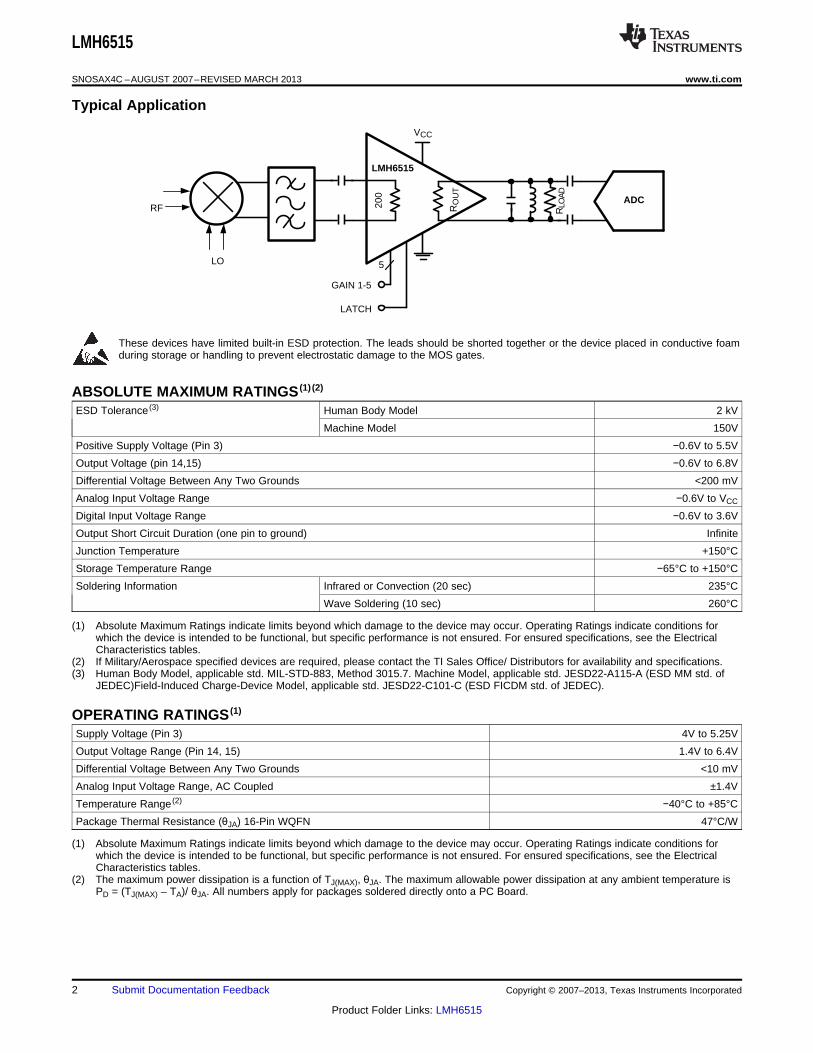
Typical Application
These devices have limited built-in ESD protection. The leads should be shorted together or the device placed in conductive foamduring storage or handling to prevent electrostatic damage to the MOS gates.
ABSOLUTE MAXIMUM RATINGS (1) (2)
ESD Tolerance (3) Human Body Model 2 kV
Machine Model 150V
Positive Supply Voltage (Pin 3) −0.6V to 5.5V
Output Voltage (pin 14,15) −0.6V to 6.8V
Differential Voltage Between Any Two Grounds <200 mV
Analog Input Voltage Range −0.6V to VCC
Digital Input Voltage Range −0.6V to 3.6V
Output Short Circuit Duration (one pin to ground) Infinite
Junction Temperature +150°C
Storage Temperature Range −65°C to +150°C
Soldering Information Infrared or Convection (20 sec) 235°C
Wave Soldering (10 sec) 260°C
(1) Absolute Maximum Ratings indicate limits beyond which damage to the device may occur. Operating Ratings indicate conditions forwhich the device is intended to be functional, but specific performance is not ensured. For ensured specifications, see the ElectricalCharacteristics tables.
(2) If Military/Aerospace specified devices are required, please contact the TI Sales Office/ Distributors for availability and specifications.(3) Human Body Model, applicable std. MIL-STD-883, Method 3015.7. Machine Model, applicable std. JESD22-A115-A (ESD MM std. of
JEDEC)Field-Induced Charge-Device Model, applicable std. JESD22-C101-C (ESD FICDM std. of JEDEC).
OPERATING RATINGS (1)
Supply Voltage (Pin 3) 4V to 5.25V
Output Voltage Range (Pin 14, 15) 1.4V to 6.4V
Differential Voltage Between Any Two Grounds <10 mV
Analog Input Voltage Range, AC Coupled ±1.4V
Temperature Range (2) −40°C to +85°C
Package Thermal Resistance (θJA) 16-Pin WQFN 47°C/W
(1) Absolute Maximum Ratings indicate limits beyond which damage to the device may occur. Operating Ratings indicate conditions forwhich the device is intended to be functional, but specific performance is not ensured. For ensured specifications, see the ElectricalCharacteristics tables.
(2) The maximum power dissipation is a function of TJ(MAX), θJA. The maximum allowable power dissipation at any ambient temperature isPD = (TJ(MAX) – TA)/ θJA. All numbers apply for packages soldered directly onto a PC Board.
2 Submit Documentation Feedback Copyright © 2007–2013, Texas Instruments Incorporated
Product Folder Links: LMH6515
LMH6515
www.ti.com SNOSAX4C –AUGUST 2007–REVISED MARCH 2013
5V ELECTRICAL CHARACTERISTICS (1)
The following specifications apply for single supply with VCC = 5V, Maximum Gain , RL = 100Ω (200Ω external || 200Ωinternal), VOUT = 2 VPP, fin = 150 MHz. Boldface limits apply at temperature extremes.
Symbol Parameter Conditions Min (2) Typ (3) Max (2) Units
Dynamic Performance
SSBW −3 dB Bandwidth Average of all Gain Settings 600 MHz
Noise and Distortion
Third Order Intermodulation Products f = 75 MHz, VOUT = 2 VPP −76
f = 150 MHz, VOUT = 2 VPP −72dBc
f = 250 MHz, VOUT = 2 VPP −66
f = 450 MHz, VOUT = 2 VPP −58
OIP3 Output 3rd Order Intercept Point f = 75 MHz, VOUT = 2 VPP, 39Tone Spacing = 0.5 MHz
f = 150 MHz, VOUT = 2 VPP, 37Tone Spacing = 2 MHz
f = 250 MHz, VOUT = 2 VPP, 34Tone Spacing = 2 MHz
dBmf = 75 MHz, RL = 200Ω, VOUT = 2 VPP, 40Tone Spacing = 0.5 MHz
f = 150 MHz, RL = 200Ω, VOUT= 2 VPP, 37Tone Spacing = 2 MHz
f = 250 MHz, RL = 200Ω, VOUT = 2 VPP, 34Tone Spacing = 2 MHz
P1 dB Output Level for 1 dB Gain f = 75 MHz, RL = 200Ω 16.7Compression f = 250 MHz, RL = 200Ω 14.7
dBmf = 75 MHz 14.5
f = 450 MHz 13.2
VNI Input Noise Voltage Maximum Gain, f = 40 MHz 1.8 nV/√Hz
VNO Output Noise Voltage Maximum Gain, f = 40 MHz 18 nV/√Hz
NF Noise Figure Maximum Gain 8.3 dB
Analog I/O
Differential Input Resistance 165 186 210 Ω160 220
Input Common Mode Resistance 825 971 1120 Ω785 1160
Differential Output Impedance Low Gain Option 187ΩHigh Gain Option 330 370 410
325 415
Internal Load Resistors Between Pins 13, 14 and Pins 15, 16 165 187 210 Ω160 235
Input Signal Level (AC Coupled) Max Gain, VO = 2 VPP, RL = 1 kΩ 126 mVPP
Maximum Differential Input Signal AC Coupled 5.6 VPP
Input Common Mode Voltage Self Biased 1.3 1.4 1.5 V1.1 1.7
Input Common Mode Voltage Range Driven Externally 0.9 to 2.0 V
Minimum Input Voltage DC 0 V
Maximum Input Voltage DC 3.3 V
(1) Electrical Table values apply only for factory testing conditions at the temperature indicated. No specified parametric performance isindicated in the electrical tables under conditions different than those tested
(2) Limits are 100% production tested at 25°C. Limits over the operating temperature range are specified through correlation usingStatistical Quality Control (SQC) methods.
(3) Typical values represent the most likely parametric norm as determined at the time of characterization. Actual typical values may varyover time and will also depend on the application and configuration. The typical values are not tested and are not specified on shippedproduction material.
Copyright © 2007–2013, Texas Instruments Incorporated Submit Documentation Feedback 3
Product Folder Links: LMH6515
LMH6515
SNOSAX4C –AUGUST 2007–REVISED MARCH 2013 www.ti.com
5V ELECTRICAL CHARACTERISTICS(1) (continued)The following specifications apply for single supply with VCC = 5V, Maximum Gain , RL = 100Ω (200Ω external || 200Ωinternal), VOUT = 2 VPP, fin = 150 MHz. Boldface limits apply at temperature extremes.
Symbol Parameter Conditions Min (2) Typ (3) Max (2) Units
Maximum Differential Output Voltage VCC = 5V, Output Common Mode = 5V 5.5 VPPSwing
VOS Output Offset Voltage All Gain Settings 30 mV
CMRR Common Mode Rejection Ratio 85 dB
PSRR Power Supply Rejection Ratio 63 83 dB61
Gain Parameters
Maximum Gain DC, Internal RL = 200Ω, 23.9 24.2 24.6 dBExternal RL = 1280Ω 23.4 24.8
Minimum Gain DC, Internal RL = 200Ω, −7.2 −6.9 −6.5 dBExternal RL = 1280Ω −7.7 −6.4
Gain Step Size DC 1.0 dB
Gain Step Error DC 0.02dB
f = 150 MHz 0.07
Cumulative Gain Step Error DC, Gain Step 31 to Gain Step 0 −0.1 0.05 0.3 dB−0.2 0.4
Gain Step Switching Time 5 ns
Digital Inputs/Timing
Logic Compatibility CMOS Logic 3.3 V
VIL Logic Input Low Voltage 0.8 V
VIH Logic Input High Voltage 2.0 V
IIH Logic Input High Input Current (4) 32 40 μA
TSU Setup Time 3 ns
THOLD Hold Time 3 ns
TPW Minimum Latch Pulse Width 10 ns
Power Requirements
ICC Total Supply Current VOUT = 0V Differential, VOUT Common 107 124 mAMode = 5V 134
Amplifier Supply Current Pin 3 Only 56 66 mA74
Output Stage Bias Currents Pins 13, 14 and Pins 15, 16; 48 58 mAVOUT Common Mode = 5 V 60
(4) Negative input current implies current flowing out of the device.
4 Submit Documentation Feedback Copyright © 2007–2013, Texas Instruments Incorporated
Product Folder Links: LMH6515
14
15
16
13
3 2 14
10 11 129
7
6
5
8
OUT-
OUT+
GA
IN_4
GA
IN_3
GA
IN_2
GA
IN_1
NC
VC
C
LAT
CH
GA
IN_0
GND
IN+
IN-
GND LOAD+
LOAD-
GND
LMH6515
www.ti.com SNOSAX4C –AUGUST 2007–REVISED MARCH 2013
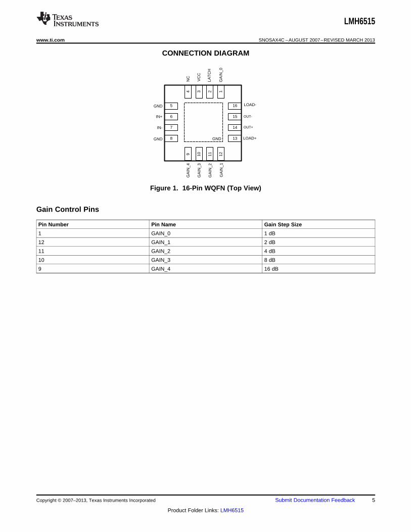
CONNECTION DIAGRAM
Figure 1. 16-Pin WQFN (Top View)
Gain Control Pins
Pin Number Pin Name Gain Step Size
1 GAIN_0 1 dB
12 GAIN_1 2 dB
11 GAIN_2 4 dB
10 GAIN_3 8 dB
9 GAIN_4 16 dB
Copyright © 2007–2013, Texas Instruments Incorporated Submit Documentation Feedback 5
Product Folder Links: LMH6515

LMH6515
SNOSAX4C –AUGUST 2007–REVISED MARCH 2013 www.ti.com
PIN DESCRIPTIONSPin Number Symbol Description
Analog I/O
6 IN+ Non-inverting analog input. Internally biased to 1.4V. Input voltage should not exceed VCC orgo below GND by more than 0.5V.
7 IN− Inverting analog input. Internally biased to 1.4V. Input voltage should not exceed VCC or gobelow GND by more than 0.5V. If using amplifier single ended this input should be capacitivelycoupled to ground.
15 OUT− Open collector inverting output. This pin is an output that also requires a power source. Thispin should be connected to 5V through either an RF choke or an appropriately sized inductorthat can form part of a filter. See APPLICATION INFORMATION section for details.
14 OUT+ Open collector non-inverting output. This pin is an output that also requires a power source.This pin should be connected to 5V through either an RF choke or an appropriately sizedinductor that can form part of a filter. See APPLICATION INFORMATION section for details.
16 LOAD− Internal 200Ω resistor connection to pin 15. This pin can be left floating for higher gain orshorted to pin 13 for lower gain and lower effective output impedance. See APPLICATIONINFORMATION section for details.
13 LOAD+ Internal 200Ω resistor connection to pin 14. This pin can be left floating for higher gain orshorted to pin 16 for lower gain and lower effective output impedance. See APPLICATIONINFORMATION section for details.
Power
3 VCC 5V power supply pin. Use ceramic, low ESR bypass capacitors. This pin powers everythingexcept the output stage.
5,8 GND Ground pins. Connect to low impedance ground plane. All pin voltages are specified withrespect to the voltage on these pins. The exposed thermal pad is also a ground connection.
6 Submit Documentation Feedback Copyright © 2007–2013, Texas Instruments Incorporated
Product Folder Links: LMH6515

LMH6515
www.ti.com SNOSAX4C –AUGUST 2007–REVISED MARCH 2013
PIN DESCRIPTIONS (continued)
Pin Number Symbol Description
Digital Inputs
1,12,11, GAIN_0 to Gain setting pins. See above table for gain step sizes for each pin. These pins are 3.3V CMOS10,9 GAIN_4 logic compatible. 5V inputs may cause damage.
2 LATCH This pin controls the function of the gain setting pins mentioned above. With LATCH in thelogic HIGH state the gain is fixed and will not change. With the LATCH in the logic LOW statethe gain is set by the state of the gain control pins. Any changes in gain made with the LATCHpin in the LOW state will take effect immediately. This pin is 3.3V CMOS logic compatible. 5Vinputs may cause damage.
4 NC This pin is not connected. It can be grounded or left floating.
Copyright © 2007–2013, Texas Instruments Incorporated Submit Documentation Feedback 7
Product Folder Links: LMH6515
0 3 6 9 12 15 18 21 24 27 3025
27
29
31
33
35
37
39
41
43
45
OIP
3 (d
Bm
)
GAIN STEP (0 = MAX GAIN)
RL = 200:
VOUT = 2 VPP f = 75 MHz
f = 150 MHz f = 250 MHz
INPUT CLIPPING
0 3 6 9 12 15 18 21 24 27 3025
27
29
31
33
35
37
39
41
43
45
OIP
3 (d
Bm
)
GAIN STEP (0 = MAX GAIN)
RL = 100:
VOUT = 2 VPP f = 75 MHz
f = 150 MHz f = 250 MHz
INPUT CLIPPING
1 10 100 1000
FREQUENCY (MHz)
15
16
17
18
19
20
GA
IN (
dB)
-40°C
25°C 85°C
1 10 100 1000
FREQUENCY (MHz)
-16
-15
-14
-13
-12
-11
GA
IN (
dB)
-40°C
25°C 85°C
10 100 1000-2
1
4
7
10
13
16
19
22
GA
IN (
dB)
FREQUENCY (MHz)
CL = 0 pF
CL = 1.8 pF
CL = 4.7 pF
CL = 10 pF
LOAD = 100: || CL
10 100 1000-19
-13
11
20
GA
IN (
dB)
17
14
-7-10
-16
-4-1
2
5
8
FREQUENCY (MHz)
RL = 100:
LMH6515
SNOSAX4C –AUGUST 2007–REVISED MARCH 2013 www.ti.com
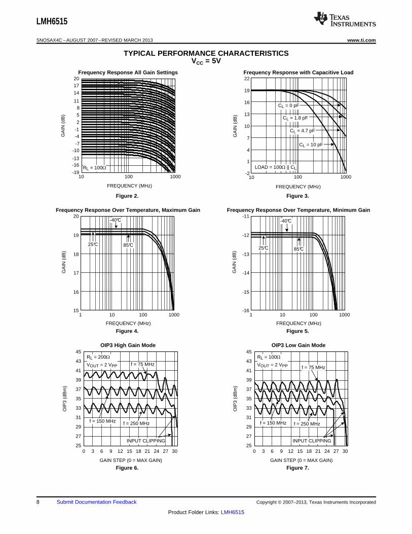
TYPICAL PERFORMANCE CHARACTERISTICSVCC = 5V
Frequency Response All Gain Settings Frequency Response with Capacitive Load
Figure 2. Figure 3.
Frequency Response Over Temperature, Maximum Gain Frequency Response Over Temperature, Minimum Gain
Figure 4. Figure 5.
OIP3 High Gain Mode OIP3 Low Gain Mode
Figure 6. Figure 7.
8 Submit Documentation Feedback Copyright © 2007–2013, Texas Instruments Incorporated
Product Folder Links: LMH6515

0 50 100 150 200 250 300 350 400 450-90
-80
-70
-60
-50
-40
-30
DIS
TO
RT
ION
(dB
c)
FREQUENCY (MHz)
RL = 100:
2.8 VPP
2 VPP
1 VPP
0 3 6 9 12 15 18 21 24 27 30-100
-90
-80
-70
-60
-50
-40
-30
-20
IMD
3 (d
Bc)
GAIN STEP (0 = MAX GAIN)
f = 150 MHz
RL = 200:
INPUT CLIPPING
2.8 VPP
2 VPP
1 VPP
0 3 6 9 12 15 18 21 24 27 30
GAIN STEP (0 = MAX GAIN)
-80
-75
-70
-65
-60
-55
-50
-45
-40
IMD
(dB
c)
RL = 100:
VOUT = 2 VPP
f = 250 MHz f = 150 MHz
f = 75 MHz
INPUT CLIPPING
0 3 6 9 12 15 18 21 24 27 30
GAIN STEP (0 = MAX GAIN)
-90
-85
-80
-75
-70
-65
-60
-55
-50
IMD
(dB
c)
RL = 200:
VOUT = 2 VPP
f = 250 MHzf = 150 MHz
f = 75 MHz
INPUT CLIPPING
-40 -20 0 20 40 60 80
TEMPERATURE (°C)
20
25
30
35
40
45
OIP
3 (d
Bm
)
75 MHz
150 MHz
250 MHz
RL = 200:
0 3 6 12 1815 219 24 27 3025
27
41
39
37
35
33
31
29
45
43
GAIN STEP (0 = MAX GAIN)
OIP
3 (d
Bm
)
f = 150 MHz
RL = 200:
VOUT = 1 VPP
VOUT = 2 VPP
VOUT = 2.8 VPP
INPUT CLIPPING
LMH6515
www.ti.com SNOSAX4C –AUGUST 2007–REVISED MARCH 2013
TYPICAL PERFORMANCE CHARACTERISTICSVCC = 5V (continued)
OIP3 Over Temperature OIP3 High Gain Mode
Figure 8. Figure 9.
IMD3 Low Gain Mode IMD3 High Gain Mode
Figure 10. Figure 11.
IMD3 High Gain Mode HD2 vs. Frequency
Figure 12. Figure 13.
Copyright © 2007–2013, Texas Instruments Incorporated Submit Documentation Feedback 9
Product Folder Links: LMH6515
0 100 200 300 400 500 600
FREQUENCY (MHz)
8
9
10
11
12
13
NO
ISE
FIG
UR
E (
dB)
0 10 20 30
GAIN SETTING (0 = MAXIMUM GAIN)
0
10
20
30
40
50
60
OU
TP
UT
NO
ISE
(nV
/H
z) RL = 200:
RL = 100:
f = 40 MHz
0 10 20 305
10
15
20
25
30
35
40
NO
ISE
FIG
UR
E (
dB)
GAIN STEP (0 = MAXIMUM GAIN)
150 MHz
70 MHz
0 50 100 150 200 250 300 350 400 450-100
-90
-80
-70
-60
-50
-40
-30
DIS
TO
RT
ION
(dB
c)
FREQUENCY (MHz)
2.8 VPP
2 VPP
1 VPP
RL = 200:
0 50 100 150 200 250 300 350 400 450-90
-80
-70
-60
-50
-40
-30
DIS
TO
RT
ION
(dB
c)
FREQUENCY (MHz)
RL = 100:
2.8 VPP
2 VPP
1 VPP
0 50 100 150 200 250 300 350 400 450-100
-90
-80
-70
-60
-50
-40
-30
DIS
TO
RT
ION
(dB
c)
FREQUENCY (MHz)
2.8 VPP
2 VPP
1 VPP
RL = 200:
LMH6515
SNOSAX4C –AUGUST 2007–REVISED MARCH 2013 www.ti.com
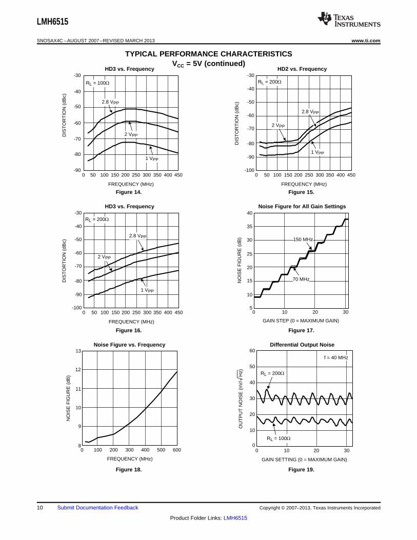
TYPICAL PERFORMANCE CHARACTERISTICSVCC = 5V (continued)
HD3 vs. Frequency HD2 vs. Frequency
Figure 14. Figure 15.
HD3 vs. Frequency Noise Figure for All Gain Settings
Figure 16. Figure 17.
Noise Figure vs. Frequency Differential Output Noise
Figure 18. Figure 19.
10 Submit Documentation Feedback Copyright © 2007–2013, Texas Instruments Incorporated
Product Folder Links: LMH6515
0 100 200 300 400 5000
0.2
0.4
0.6
0.8
1
1.2
1.4
1.6
GA
IN S
TE
P E
RR
OR
(dB
)
FREQUENCY (MHz)
RL = 200:
0 50 100 150 200 250 300
FREQUENCY (MHz)
0
0.05
0.1
0.15
0.2
0.25
0.3
0.35
0.4
ER
RO
R (
dB)
RL = 100:
85°C
25°C
-40°C
-50 -25 0 25 50 75 100
TEMPERATURE (°C)
17
17.5
18
18.5
19
19.5
MA
XIM
UM
GA
IN (
dB)
125
f = 70 MHz
f = 150 MHz
f = 250 MHz
f = 450 MHz
RL = 100:
0 100 200 300 400 5000
0.05
0.1
0.15
0.2
0.25
0.3
0.35
0.4
0.45
0.5
GA
IN S
TE
P E
RR
OR
(dB
)
FREQUENCY (MHz)
RL = 100:
3.5 4 4.5 5 5.524
24.2
24.4
24.6
24.8
25
25.2
25.4
25.6
25.8
26
MA
XIM
UM
GA
IN, H
IGH
GA
IN M
OD
E (
dB)
SUPPLY VOLTAGE (V)
18
18.2
18.4
18.6
18.8
19
19.2
19.4
19.6
19.8
20
MA
XIM
UM
GA
IN, L
OW
GA
IN M
OD
E (
dB)
PIN = -24 dBmf = 75 MHz
LOW GAIN MODE, RL = 100:
HIGH GAIN MODE, RL = 200:
10 100 1k 10k 100k
EXTERNAL DIFFERENTIAL LOAD (:)
12
16
20
24
28
32
36
MA
XIM
UM
GA
IN (
dB)
400: INTERNAL WITH 400: EXTERNAL = 26 dB NET
200: INTERNAL WITH 200: EXTERNAL = 20 dB NET
INTERNAL LOAD = 200:
INTERNAL LOAD = 400:
LMH6515
www.ti.com SNOSAX4C –AUGUST 2007–REVISED MARCH 2013
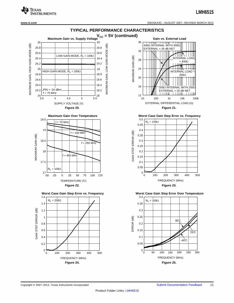
TYPICAL PERFORMANCE CHARACTERISTICSVCC = 5V (continued)
Maximum Gain vs. Supply Voltage Gain vs. External Load
Figure 20. Figure 21.
Maximum Gain Over Temperature Worst Case Gain Step Error vs. Frequency
Figure 22. Figure 23.
Worst Case Gain Step Error vs. Frequency Worst Case Gain Step Error Over Temperature
Figure 24. Figure 25.
Copyright © 2007–2013, Texas Instruments Incorporated Submit Documentation Feedback 11
Product Folder Links: LMH6515

0 10 20 30 40 50 60 70 80 90 100-0.6
-0.3
0
0.3
0.6
VO
UT (
V)
TIME (ns)
3
2
1
0
LAT
CH
(V
)
LATCH
VOUT
0 10 20 30 40 50 60 70 80 90 100-0.6
-0.3
0
0.3
0.6
VO
UT (
V)
TIME (ns)
3
2
1
0
LAT
CH
(V
)
LATCH
VOUT
1 10 100 1000
FREQUENCY (MHz)
-90
-80
-70
-60
-50
-40
-30
CR
OS
ST
ALK
(dB
c)
PIN = -10 dBmLOAD = 200:MAX GAIN
LATCH
GAIN 1
0 10 20 30 40 50 60 70 80 90 100-0.6
-0.3
0
0.3
0.6
VO
UT (
V)
TIME (ns)
3
2
1
0
LAT
CH
(V
)
LATCH
VOUT
0 10 20 30 40 50 60 70 80 90 100-40
-30
-20
-10
0
10
20
30
40
DIF
FE
RE
NT
IAL
OU
TP
UT
(m
V)
TIME (ns)
0
3
GA
IN C
ON
TR
OL
SIG
NA
LS (
V)
LATCH = 0
PINS 9, 10, 11,12
0 10 20 30 40 50 60 70 80 90 100-40
-30
-20
-10
0
10
20
30
40
DIF
FE
RE
NT
IAL
OU
TP
UT
(m
V)
TIME (ns)
0
3
GA
IN C
ON
TR
OL
SIG
NA
LS (
V)
LATCH = 3.3V
PINS 9, 10, 11,12
LMH6515
SNOSAX4C –AUGUST 2007–REVISED MARCH 2013 www.ti.com
TYPICAL PERFORMANCE CHARACTERISTICSVCC = 5V (continued)
Digital Crosstalk Digital Crosstalk
Figure 26. Figure 27.
Minimum Gain to Maximum Gain SwitchingDigital Pin to Output Isolation Using Latch Pin
Figure 28. Figure 29.
Maximum Gain to Minimum Gain SwitchingUsing Latch Pin 16 dB Gain Step Using Latch Pin
Figure 30. Figure 31.
12 Submit Documentation Feedback Copyright © 2007–2013, Texas Instruments Incorporated
Product Folder Links: LMH6515

-10 -5 0 5 10 15 20 25 30
TIME (Ps)
-0.4
-0.3
-0.2
-0.1
0
0.1
0.2
0.3
0.4
VO
UT (
V)
f = 250 MHzENVELOPE DISPLAYED
VOUT
V+
0
1
2
3
4
5
6
PO
WE
R S
UP
PLY
(V
)
-10 -5 0 5 10 15 20 25 30
TIME (Ps)
-0.4
-0.3
-0.2
-0.1
0
0.1
0.2
0.3
0.4
VO
UT (
V)
f = 250 MHzENVELOPE DISPLAYED
VOUT
V+
0
1
2
3
4
5
6P
OW
ER
SU
PP
LY (
V)
0 10 20 30 40 50 60 70 80 90 100-0.6
-0.3
0
0.3
0.6
VO
UT (
V)
TIME (ns)
3
2
1
0
LAT
CH
(V
)
LATCH
VOUT
-10 -5 0 5 10 15 20 25 30
TIME (Ps)
-0.4
-0.3
-0.2
-0.1
0
0.1
0.2
0.3
0.4
VO
UT (
V)
f = 250 MHzENVELOPE DISPLAYED
VOUT
V+
0
1
2
3
4
5
6
PO
WE
R S
UP
PLY
(V
)
0 10 20 30 40 50 60 70 80 90 100-0.6
-0.3
0
0.3
0.6
VO
UT (
V)
TIME (ns)
3
2
1
0
GA
IN P
IN V
IN (
V)
GAIN BIT 4
VOUT
0 10 20 30 40 50 60 70 80 90 100-0.6
-0.3
0
0.3
0.6
VO
UT (
V)
TIME (ns)
3
2
1
0
GA
IN P
IN V
IN (
V)
GAIN BIT 3
VOUT
LMH6515
www.ti.com SNOSAX4C –AUGUST 2007–REVISED MARCH 2013
TYPICAL PERFORMANCE CHARACTERISTICSVCC = 5V (continued)
16 dB Gain Step with Latch Pin Low 8 dB Gain Step with Latch Pin LowSwitching Gain Pin 4 Switching Gain Pin 3
Figure 32. Figure 33.
4 dB Gain Step Using Latch Pin Power On Timing, Maximum Gain
Figure 34. Figure 35.
Power On Timing, Minimum Gain Power Off Timing, Maximum Gain
Figure 36. Figure 37.
Copyright © 2007–2013, Texas Instruments Incorporated Submit Documentation Feedback 13
Product Folder Links: LMH6515
-10 -5 0 5 10 15 20 25 30
TIME (Ps)
-0.4
-0.3
-0.2
-0.1
0
0.1
0.2
0.3
0.4
VO
UT (
V)
f = 250 MHzENVELOPE DISPLAYED
VOUT
V+
0
1
2
3
4
5
6
PO
WE
R S
UP
PLY
(V
)
LMH6515
SNOSAX4C –AUGUST 2007–REVISED MARCH 2013 www.ti.com
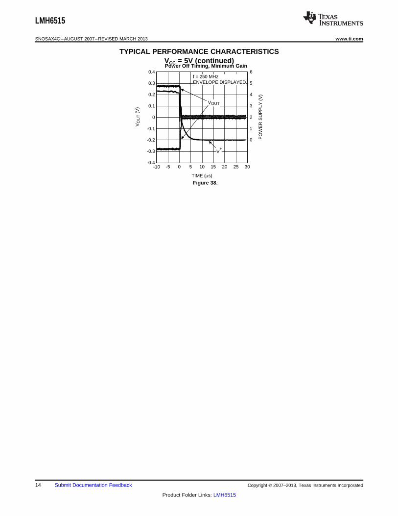
TYPICAL PERFORMANCE CHARACTERISTICSVCC = 5V (continued)Power Off Timing, Minimum Gain
Figure 38.
14 Submit Documentation Feedback Copyright © 2007–2013, Texas Instruments Incorporated
Product Folder Links: LMH6515

6
7
5, 8
+IN
-IN
OUT- OUT+
VARIABLEATTENUATOR
0 to -31 dB
+32 dB
200:
200: 200:
400:
13
14
16
15
+-
GAIN 1-5
200
ADC200
5
LATCH
LMH6515
VCC
V = VCM CC
44.3 nH
10 pF
VCC
LMH6515
www.ti.com SNOSAX4C –AUGUST 2007–REVISED MARCH 2013
APPLICATION INFORMATION
The LMH6515 is a fully differential amplifier optimized for signal path applications up to 400 MHz. The LMH6515has a 200Ω input. The absolute gain is load dependent, however the gain steps are always 1 dB. The LMH6515output stage is a class A amplifier. This class A operation results in excellent distortion and linearitycharacteristics. This makes the LMH6515 ideal for voltage amplification and an ideal ADC driver where highlinearity is necessary.
Figure 39. LMH6515 Typical Application
The LMH6515 output common mode should be set carefully. Using inductors to set the output common mode isone preferred method and will give maximum output swing. AC coupling of the output is recommended. Theinductors mentioned above will shift the idling output common mode to the positive supply. Also, with theinductors, the output voltage can exceed the supply voltage. Other options for setting the output common moderequire supply voltages above 5V. If using a supply higher than 5V care should be taken to make sure the outputcommon mode does not exceed the 5.25V supply rating.
It is also important to note the maximum voltage limits for the OUT+ and OUT− pins, which is 6.4V. When usinginductors these pins will experience voltage swings beyond the supply voltage. With a 5V output common modeoperating point this makes the effective maximum swing 5.6 VPP differential. System calibration and automaticgain control algorithms should be tailored to avoid exceeding this limit.
In order to help with system design TI offers the ADC14V155KDRB High IF Receiver reference design board.This board combines the LMH6515 DVGA with the ADC14V155 ADC and provides a ready made solution formany IF receiver applications. Using an IF frequency of 169 MHz it achieves a small signal SNR of 72 dBFS andan SFDR of greater than 90 DBFS. Large signal measurements show an SNR of 68 dBFS and an SFDR of 77dBFS. The High IF Receiver board also features the LMK03000 low-jitter precision clock conditioner.
Figure 40. LMH6515 Block Diagram
Copyright © 2007–2013, Texas Instruments Incorporated Submit Documentation Feedback 15
Product Folder Links: LMH6515

GAIN 1-5
200
5
LATCH
LMH6515
5V
Vin
R1RIN = R1 || 200
INTERNAL BIAS = 1.4V
C1
C2
LMH6515
SNOSAX4C –AUGUST 2007–REVISED MARCH 2013 www.ti.com
INPUT CHARACTERISTICS
The LMH6515 input impedance is set by internal resistors to a nominal 200Ω. Process variations will result in arange of values as shown in the 5V Electrical Characteristics table. At higher frequencies parasitics will start toimpact the impedance. This characteristic will also depend on board layout and should be verified on thecustomer’s system board.
At maximum gain the digital attenuator is set to 0 dB and the input signal will be much smaller than the output. Atminimum gain the output is 12 dB or more smaller than the input. In this configuration the input signal size maylimit the amplifier output amplitude, depending on the output configuration and the desired output signal voltage.The input signal cannot swing more than 0.5V below the negative supply voltage (normally 0V) nor should itexceed the positive supply voltage. The input signal will clip and cause severe distortion if it is too large. Becausethe input stage self biases to approximately 1.4V the lower supply voltage will impose the limit for input voltageswing. To drive larger input signals the input common mode can be forced higher than 1.4V to allow for moreswing. An input common mode of 2.0V will allow an 8 VPP maximum input signal. The trade off for input signalswing is that as the input common mode is shifted away from the 1.4V internal bias point the distortionperformance will suffer slightly.
(Note capacitor on grounded input)
Figure 41. Single Ended Input
OUTPUT CHARACTERISTICS
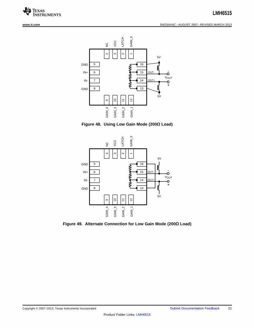
The LMH6515 has the option of two different output configurations. The LMH6515 is an open collector topology.As shown in Figure 46 each output has an on chip 200Ω pull up resistor. In addition there is an internal 400Ωresistor between the two outputs. This results in a 200Ω or a 400Ω differential load in parallel with the externalload. The 400Ω option is the high gain option and the 200Ω provides for less gain. The 200Ω configuration isrecommended unless more gain is required.
The output common mode of the LMH6515 must be set by external components. Most applications will benefitfrom the use of inductors on the output stage. In particular, the 400Ω option, as shown in Figure 47, will requireinductors in order to be able to develop an output voltage. The 200Ω option as shown in Figure 48 or Figure 49will also require inductors since the voltage drop due to the on chip 200Ω resistors will saturate the outputtransistors. It is also possible to use resistors and high voltage power supplies to set the output common mode.This operation is not recommended, unless it is necessary to DC couple the output. If DC coupling is required theinput common mode and output common mode voltages must be taken into account.
Maximum bandwidth with the LMH6515 is achieved by using the low gain, low impedance output option andusing a low load resistance. With an effective load of 67Ω a bandwidth of nearly 1 GHz can be realized. As theeffective resistance on the output stage goes up the capacitance of the board traces and amplifier output stagelimit bandwidth in a roughly linear fashion. At an output impedance of 100Ω the bandwidth is down to 600 MHz,and at 200Ω the bandwidth is 260 MHz. For this reason driving very high impedance loads is not recommended.
Although bandwidth goes down with higher values of load resistance, the distortion performance improves andgain increases. The LMH6515 has a common emitter Class A output stage and minimizing the amount of currentswing in the output devices improves distortion substantially.
16 Submit Documentation Feedback Copyright © 2007–2013, Texas Instruments Incorporated
Product Folder Links: LMH6515
10 100 1k 10k 100k
EXTERNAL DIFFERENTIAL LOAD (:)
12
16
20
24
28
32
36
MA
XIM
UM
GA
IN (
dB)
400: INTERNAL WITH 400: EXTERNAL = 26 dB NET
200: INTERNAL WITH 200: EXTERNAL = 20 dB NET
INTERNAL LOAD = 200:
INTERNAL LOAD = 400:
1 10 100 1000 10000
FREQUENCY (MHz)
-9
-8
-7
-6
-5
-4
-3
-2
-1
0
1N
OR
MA
LIZ
ED
GA
IN (
dB)
RL = 100: TOTAL
1 PH
470 nH
200 nH
LMH6515
www.ti.com SNOSAX4C –AUGUST 2007–REVISED MARCH 2013
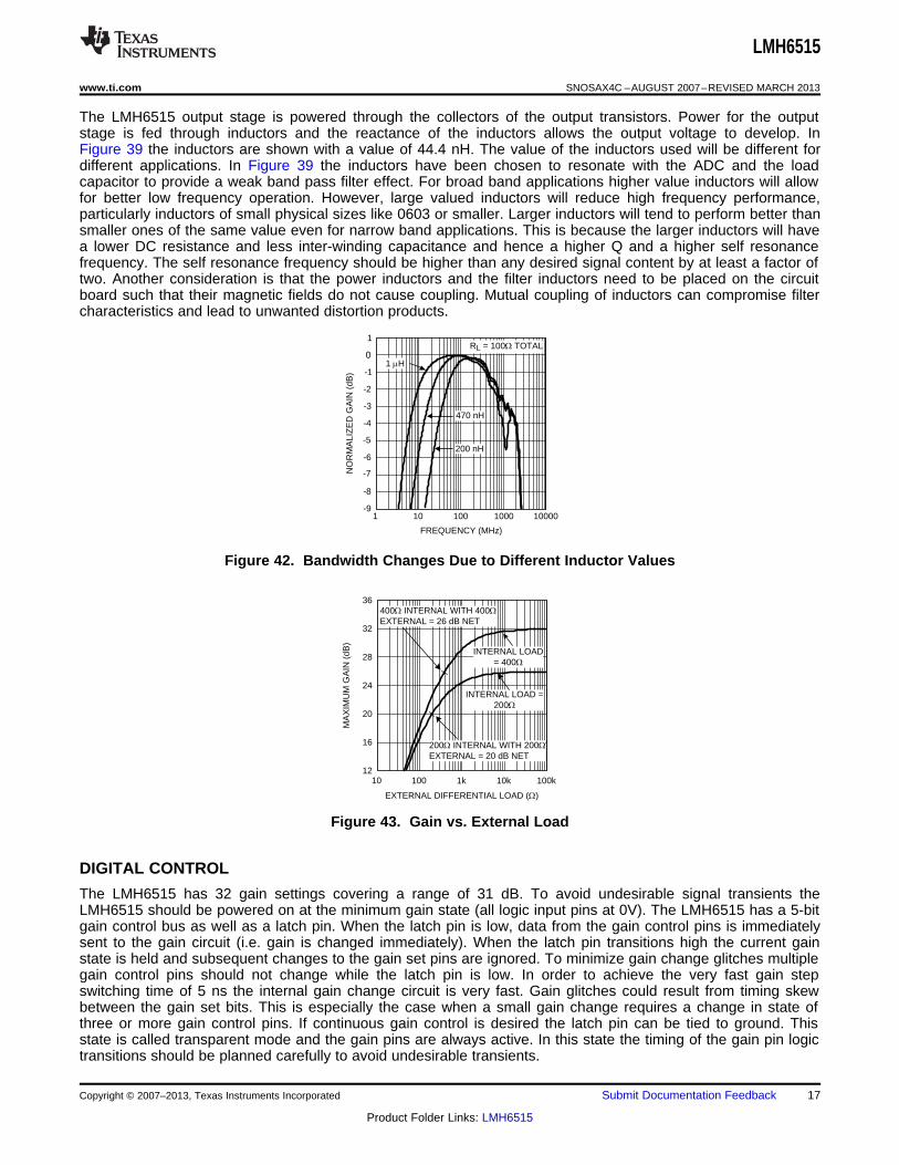
The LMH6515 output stage is powered through the collectors of the output transistors. Power for the outputstage is fed through inductors and the reactance of the inductors allows the output voltage to develop. InFigure 39 the inductors are shown with a value of 44.4 nH. The value of the inductors used will be different fordifferent applications. In Figure 39 the inductors have been chosen to resonate with the ADC and the loadcapacitor to provide a weak band pass filter effect. For broad band applications higher value inductors will allowfor better low frequency operation. However, large valued inductors will reduce high frequency performance,particularly inductors of small physical sizes like 0603 or smaller. Larger inductors will tend to perform better thansmaller ones of the same value even for narrow band applications. This is because the larger inductors will havea lower DC resistance and less inter-winding capacitance and hence a higher Q and a higher self resonancefrequency. The self resonance frequency should be higher than any desired signal content by at least a factor oftwo. Another consideration is that the power inductors and the filter inductors need to be placed on the circuitboard such that their magnetic fields do not cause coupling. Mutual coupling of inductors can compromise filtercharacteristics and lead to unwanted distortion products.
Figure 42. Bandwidth Changes Due to Different Inductor Values
Figure 43. Gain vs. External Load
DIGITAL CONTROL
The LMH6515 has 32 gain settings covering a range of 31 dB. To avoid undesirable signal transients theLMH6515 should be powered on at the minimum gain state (all logic input pins at 0V). The LMH6515 has a 5-bitgain control bus as well as a latch pin. When the latch pin is low, data from the gain control pins is immediatelysent to the gain circuit (i.e. gain is changed immediately). When the latch pin transitions high the current gainstate is held and subsequent changes to the gain set pins are ignored. To minimize gain change glitches multiplegain control pins should not change while the latch pin is low. In order to achieve the very fast gain stepswitching time of 5 ns the internal gain change circuit is very fast. Gain glitches could result from timing skewbetween the gain set bits. This is especially the case when a small gain change requires a change in state ofthree or more gain control pins. If continuous gain control is desired the latch pin can be tied to ground. Thisstate is called transparent mode and the gain pins are always active. In this state the timing of the gain pin logictransitions should be planned carefully to avoid undesirable transients.
Copyright © 2007–2013, Texas Instruments Incorporated Submit Documentation Feedback 17
Product Folder Links: LMH6515

AM
P R
OU
T
680 nH
680 nH
5V
5V
390 nH
390 nH 3 pF
41 pF 27 nH
200
ADC CIN 200:
3 pF
LMH6515
SNOSAX4C –AUGUST 2007–REVISED MARCH 2013 www.ti.com
The LMH6515 was designed to interface with 3.3V CMOS logic circuits. If operation with 5V logic is required asimple voltage divider at each logic pin will allow for this. To properly terminate 100Ω transmission lines a dividerwith a 66.5Ω resistor to ground and a 33.2Ω series resistor will properly terminate the line as well as give the3.3V logic levels. Care should be taken not to exceed the 3.6V absolute maximum voltage rating of the logicpins.
EXPOSED PAD WQFN PACKAGE
The LMH6515 is in a thermally enhanced package. The exposed pad is connected to the GND pins. It isrecommended, but not necessary, that the exposed pad be connected to the supply ground plane. In any case,the thermal dissipation of the device is largely dependent on the attachment of this pad. The exposed pad shouldbe attached to as much copper on the circuit board as possible, preferably external copper. However, it is alsovery important to maintain good high speed layout practices when designing a system board. Please refer to theLMH6515 evaluation board for suggested layout techniques.
Package information is available on the TI Web site.www.ti.com/packaging
INTERFACING TO ADC
The LMH6515 was designed to be used with high speed ADCs such as the ADC14155. As shown in the TypicalApplication schematic, AC coupling provides the best flexibility especially for IF sub-sampling applications. Anyresistive networks on the output will also cause a gain loss because the output signal is developed across theoutput resistors. The chart Maximum Gain vs. External Load shows the change in gain when an external load isadded.
The inputs of the LMH6515 will self bias to the optimum voltage for normal operation. The internal bias voltagefor the inputs is approximately 1.4V. In most applications the LMH6515 input will need to be AC coupled.
The output common mode voltage is not self biasing, it needs to be pulled up to the positive supply rail withexternal inductors as shown in Figure 39. This gives the LMH6515 the capability for large signal swings with verylow distortion on a single 5V supply. The internal load resistors provide the LMH6515 with very consistent gain.
A unique internal architecture allows the LMH6515 to be driven by either a differential or single ended source. Ifdriving the LMH6515 single ended, the unused input should be terminated to ground with a 0.01 µF capacitor.Directly shorting the unused input to ground will disrupt the internal bias circuitry and will result in poorperformance.
Figure 44. Bandpass FilterCenter Frequency is 140 MHz with a 20 MHz Bandwidth
Designed for 200Ω Impedance
18 Submit Documentation Feedback Copyright © 2007–2013, Texas Instruments Incorporated
Product Folder Links: LMH6515

AM
P Z
OU
T
L2
L1
5V
5V
L4
L3C1
C2
C3
L5
AD
C Z
IN
R1
ADC VIN +
ADC VIN -
ADC VCM
AMP VOUT -
AMP VOUT +
R2
LMH6515
www.ti.com SNOSAX4C –AUGUST 2007–REVISED MARCH 2013
ADC Noise Filter
Figure 44 shows a filter schematic and the following table of values are for some common IF frequencies. Thefilter shown offers a good compromise between bandwidth, noise rejection and cost. This filter topology is thesame as used on the ADC14V155KDRB High IF Receiver reference design board. This filter topology works bestwith the 12 and 14-bit sub-sampling analog to digital converters shown in the Table 2 table.
Table 1. Filter Component Values
Filter Component Values
Fc 75 140 170 250MHz MHz MHz MHz
BW 40 20 25 Narrow BandMHz MHz MHz
Components L1, L2 10 µH 10 µH 10 µH 10 µH
L3, L4 390 nH 390 nH 560 nH —
C1, C2 10 pF 3 pF 1.4 pF 47 pF
C3 22 pF 41 pF 32 pF 11 pF
L5 220 nH 27 nH 30 nH 22 nH
R1, R2 100 200 100 499
Figure 45. Sample Filter
POWER SUPPLIES
As shown in Figure 46, the LMH6515 has a number of options for power supply connections on the output pins.Pin 3 (VCC) is always connected. The output stage can be connected as shown in Figure 47, Figure 48, orFigure 49. The supply voltage range for VCC is 4V to 5.25V. A 5V supply provides the best performance whilelower supplies will result in less power consumption. Power supply regulation of 2.5% or better is advised.
Of special note is that the digital circuits are powered from an internal supply voltage of 3.3V. The logic pinsshould not be driven above the absolute maximum value of 3.6V. See the DIGITAL CONTROL section fordetails.
Copyright © 2007–2013, Texas Instruments Incorporated Submit Documentation Feedback 19
Product Folder Links: LMH6515

14
15
16
13
3 2 14
10 11 129
7
6
5
8
OUT-
OUT+
GA
IN_4
GA
IN_3
GA
IN_2
GA
IN_1
NC
VC
C
LAT
CH
GA
IN_0
GND
IN+
IN-
GND NC
NC
-
+
VOUT
5V
5V
14
15
16
13
3 2 14
10 11 129
7
6
5
8
OUT-
OUT+
GA
IN_4
GA
IN_3
GA
IN_2
GA
IN_1
NC
VC
C
LAT
CH
GA
IN_0
GND
IN+
IN-
GND LOAD+
LOAD-
LMH6515
SNOSAX4C –AUGUST 2007–REVISED MARCH 2013 www.ti.com
Figure 46. Internal Load Resistors
Figure 47. Using High Gain Mode (400Ω Load)
20 Submit Documentation Feedback Copyright © 2007–2013, Texas Instruments Incorporated
Product Folder Links: LMH6515
14
15
16
13
3 2 14
10 11 129
7
6
5
8
OUT-
OUT+
GA
IN_4
GA
IN_3
GA
IN_2
GA
IN_1
NC
VC
C
LAT
CH
GA
IN_0
GND
IN+
IN-
GND
-
+
VOUT
5V
5V
14
15
16
13
3 2 14
10 11 129
7
6
5
8
OUT-
OUT+
GA
IN_4
GA
IN_3
GA
IN_2
GA
IN_1
NC
VC
C
LAT
CH
GA
IN_0
GND
IN+
IN-
GND
-
+
VOUT
5V
5V
LMH6515
www.ti.com SNOSAX4C –AUGUST 2007–REVISED MARCH 2013
Figure 48. Using Low Gain Mode (200Ω Load)
Figure 49. Alternate Connection for Low Gain Mode (200Ω Load)
Copyright © 2007–2013, Texas Instruments Incorporated Submit Documentation Feedback 21
Product Folder Links: LMH6515

LMH6515
SNOSAX4C –AUGUST 2007–REVISED MARCH 2013 www.ti.com
Table 2. Compatible High Speed Analog to Digital Converters
Product Number Max Sampling Rate (MSPS) Resolution Channels
ADC12L063 62 12 SINGLE
ADC12DL065 65 12 DUAL
ADC12L066 66 12 SINGLE
ADC12DL066 66 12 DUAL
CLC5957 70 12 SINGLE
ADC12L080 80 12 SINGLE
ADC12DL080 80 12 DUAL
ADC12C080 80 12 SINGLE
ADC12C105 105 12 SINGLE
ADC12C170 170 12 SINGLE
ADC12V170 170 12 SINGLE
ADC14C080 80 14 SINGLE
ADC14C105 105 14 SINGLE
ADC14DS105 105 14 DUAL
ADC14155 155 14 SINGLE
ADC14V155 155 14 SINGLE
ADC08D500 500 8 DUAL
ADC08500 500 8 SINGLE
ADC08D1000 1000 8 DUAL
ADC081000 1000 8 SINGLE
ADC08D1500 1500 8 DUAL
ADC081500 1500 8 SINGLE
ADC08(B)3000 3000 8 SINGLE
ADC08L060 60 8 SINGLE
ADC08060 60 8 SINGLE
ADC10DL065 65 10 DUAL
ADC10065 65 10 SINGLE
ADC10080 80 10 SINGLE
ADC08100 100 8 SINGLE
ADCS9888 170 8 SINGLE
ADC08(B)200 200 8 SINGLE
ADC11C125 125 11 SINGLE
ADC11C170 170 11 SINGLE
22 Submit Documentation Feedback Copyright © 2007–2013, Texas Instruments Incorporated
Product Folder Links: LMH6515

LMH6515
www.ti.com SNOSAX4C –AUGUST 2007–REVISED MARCH 2013
REVISION HISTORY
Changes from Revision B (March 2013) to Revision C Page
• Changed layout of National Data Sheet to TI format .......................................................................................................... 21
Copyright © 2007–2013, Texas Instruments Incorporated Submit Documentation Feedback 23
Product Folder Links: LMH6515

PACKAGE OPTION ADDENDUM
www.ti.com 24-Sep-2015
Addendum-Page 1
PACKAGING INFORMATION
Orderable Device Status(1)
Package Type PackageDrawing
Pins PackageQty
Eco Plan(2)
Lead/Ball Finish(6)
MSL Peak Temp(3)
Op Temp (°C) Device Marking(4/5)
Samples
LMH6515SQ/NOPB ACTIVE WQFN RGH 16 1000 Green (RoHS& no Sb/Br)
CU SN Level-3-260C-168 HR -40 to 85 L6515SQ
(1) The marketing status values are defined as follows:ACTIVE: Product device recommended for new designs.LIFEBUY: TI has announced that the device will be discontinued, and a lifetime-buy period is in effect.NRND: Not recommended for new designs. Device is in production to support existing customers, but TI does not recommend using this part in a new design.PREVIEW: Device has been announced but is not in production. Samples may or may not be available.OBSOLETE: TI has discontinued the production of the device.
(2) Eco Plan - The planned eco-friendly classification: Pb-Free (RoHS), Pb-Free (RoHS Exempt), or Green (RoHS & no Sb/Br) - please check http://www.ti.com/productcontent for the latest availabilityinformation and additional product content details.TBD: The Pb-Free/Green conversion plan has not been defined.Pb-Free (RoHS): TI's terms "Lead-Free" or "Pb-Free" mean semiconductor products that are compatible with the current RoHS requirements for all 6 substances, including the requirement thatlead not exceed 0.1% by weight in homogeneous materials. Where designed to be soldered at high temperatures, TI Pb-Free products are suitable for use in specified lead-free processes.Pb-Free (RoHS Exempt): This component has a RoHS exemption for either 1) lead-based flip-chip solder bumps used between the die and package, or 2) lead-based die adhesive used betweenthe die and leadframe. The component is otherwise considered Pb-Free (RoHS compatible) as defined above.Green (RoHS & no Sb/Br): TI defines "Green" to mean Pb-Free (RoHS compatible), and free of Bromine (Br) and Antimony (Sb) based flame retardants (Br or Sb do not exceed 0.1% by weightin homogeneous material)
(3) MSL, Peak Temp. - The Moisture Sensitivity Level rating according to the JEDEC industry standard classifications, and peak solder temperature.
(4) There may be additional marking, which relates to the logo, the lot trace code information, or the environmental category on the device.
(5) Multiple Device Markings will be inside parentheses. Only one Device Marking contained in parentheses and separated by a "~" will appear on a device. If a line is indented then it is a continuationof the previous line and the two combined represent the entire Device Marking for that device.
(6) Lead/Ball Finish - Orderable Devices may have multiple material finish options. Finish options are separated by a vertical ruled line. Lead/Ball Finish values may wrap to two lines if the finishvalue exceeds the maximum column width.
Important Information and Disclaimer:The information provided on this page represents TI's knowledge and belief as of the date that it is provided. TI bases its knowledge and belief on informationprovided by third parties, and makes no representation or warranty as to the accuracy of such information. Efforts are underway to better integrate information from third parties. TI has taken andcontinues to take reasonable steps to provide representative and accurate information but may not have conducted destructive testing or chemical analysis on incoming materials and chemicals.TI and TI suppliers consider certain information to be proprietary, and thus CAS numbers and other limited information may not be available for release.
In no event shall TI's liability arising out of such information exceed the total purchase price of the TI part(s) at issue in this document sold by TI to Customer on an annual basis.

PACKAGE OPTION ADDENDUM
www.ti.com 24-Sep-2015
Addendum-Page 2

TAPE AND REEL INFORMATION
*All dimensions are nominal
Device PackageType
PackageDrawing
Pins SPQ ReelDiameter
(mm)
ReelWidth
W1 (mm)
A0(mm)
B0(mm)
K0(mm)
P1(mm)
W(mm)
Pin1Quadrant
LMH6515SQ/NOPB WQFN RGH 16 1000 178.0 12.4 4.3 4.3 1.3 8.0 12.0 Q1
PACKAGE MATERIALS INFORMATION
www.ti.com 20-Sep-2016
Pack Materials-Page 1

*All dimensions are nominal
Device Package Type Package Drawing Pins SPQ Length (mm) Width (mm) Height (mm)
LMH6515SQ/NOPB WQFN RGH 16 1000 210.0 185.0 35.0
PACKAGE MATERIALS INFORMATION
www.ti.com 20-Sep-2016
Pack Materials-Page 2

www.ti.com
PACKAGE OUTLINE
C
SEE TERMINALDETAIL
16X 0.30.2
2.6 0.1
16X 0.50.3
0.8 MAX
(A) TYP
0.050.00
12X 0.5
4X1.5
B 4.13.9
A
4.13.9
0.30.2
0.50.3
WQFN - 0.8 mm max heightRGH0016APLASTIC QUAD FLATPACK - NO LEAD
4214978/B 01/2017
DIM A OPT 1 OPT 1(0.1) (0.2)
PIN 1 INDEX AREA
0.08
SEATING PLANE
1
49
12
5 8
16 13(OPTIONAL)
PIN 1 ID
0.1 C A B0.05
EXPOSEDTHERMAL PAD
17 SYMM
SYMM
NOTES: 1. All linear dimensions are in millimeters. Any dimensions in parenthesis are for reference only. Dimensioning and tolerancing per ASME Y14.5M. 2. This drawing is subject to change without notice. 3. The package thermal pad must be soldered to the printed circuit board for optimal thermal and mechanical performance.
SCALE 3.000
DETAILOPTIONAL TERMINAL
TYPICAL
www.ti.com
EXAMPLE BOARD LAYOUT
0.07 MINALL AROUND
0.07 MAXALL AROUND
16X (0.25)
16X (0.6)
( 0.2) TYPVIA
12X (0.5)
(3.8)
(3.8)
(1)
( 2.6)
(R0.05)TYP
(1)
WQFN - 0.8 mm max heightRGH0016APLASTIC QUAD FLATPACK - NO LEAD
4214978/B 01/2017
SYMM
1
4
5 8
9
12
1316
SYMM
LAND PATTERN EXAMPLEEXPOSED METAL SHOWN
SCALE:15X
17
NOTES: (continued) 4. This package is designed to be soldered to a thermal pad on the board. For more information, see Texas Instruments literature number SLUA271 (www.ti.com/lit/slua271).5. Vias are optional depending on application, refer to device data sheet. If any vias are implemented, refer to their locations shown on this view. It is recommended that vias under paste be filled, plugged or tented.
SOLDER MASKOPENING
METAL UNDERSOLDER MASK
SOLDER MASKDEFINED
EXPOSED METALMETAL
SOLDER MASKOPENING
SOLDER MASK DETAILS
NON SOLDER MASKDEFINED
(PREFERRED)
EXPOSED METAL

www.ti.com
EXAMPLE STENCIL DESIGN
16X (0.6)
16X (0.25)
12X (0.5)
(3.8)
(3.8)
4X ( 1.15)
(0.675)TYP
(0.675) TYP
(R0.05)TYP
WQFN - 0.8 mm max heightRGH0016APLASTIC QUAD FLATPACK - NO LEAD
4214978/B 01/2017
NOTES: (continued) 6. Laser cutting apertures with trapezoidal walls and rounded corners may offer better paste release. IPC-7525 may have alternate design recommendations.
SYMM
TYPEXPOSED METAL
SOLDER PASTE EXAMPLEBASED ON 0.125 mm THICK STENCIL
EXPOSED PAD 17
78% PRINTED SOLDER COVERAGE BY AREA UNDER PACKAGESCALE:20X
SYMM
1
4
5 8
9
12
1316
17

IMPORTANT NOTICE
Texas Instruments Incorporated (TI) reserves the right to make corrections, enhancements, improvements and other changes to itssemiconductor products and services per JESD46, latest issue, and to discontinue any product or service per JESD48, latest issue. Buyersshould obtain the latest relevant information before placing orders and should verify that such information is current and complete.TI’s published terms of sale for semiconductor products (http://www.ti.com/sc/docs/stdterms.htm) apply to the sale of packaged integratedcircuit products that TI has qualified and released to market. Additional terms may apply to the use or sale of other types of TI products andservices.Reproduction of significant portions of TI information in TI data sheets is permissible only if reproduction is without alteration and isaccompanied by all associated warranties, conditions, limitations, and notices. TI is not responsible or liable for such reproduceddocumentation. Information of third parties may be subject to additional restrictions. Resale of TI products or services with statementsdifferent from or beyond the parameters stated by TI for that product or service voids all express and any implied warranties for theassociated TI product or service and is an unfair and deceptive business practice. TI is not responsible or liable for any such statements.Buyers and others who are developing systems that incorporate TI products (collectively, “Designers”) understand and agree that Designersremain responsible for using their independent analysis, evaluation and judgment in designing their applications and that Designers havefull and exclusive responsibility to assure the safety of Designers' applications and compliance of their applications (and of all TI productsused in or for Designers’ applications) with all applicable regulations, laws and other applicable requirements. Designer represents that, withrespect to their applications, Designer has all the necessary expertise to create and implement safeguards that (1) anticipate dangerousconsequences of failures, (2) monitor failures and their consequences, and (3) lessen the likelihood of failures that might cause harm andtake appropriate actions. Designer agrees that prior to using or distributing any applications that include TI products, Designer willthoroughly test such applications and the functionality of such TI products as used in such applications.TI’s provision of technical, application or other design advice, quality characterization, reliability data or other services or information,including, but not limited to, reference designs and materials relating to evaluation modules, (collectively, “TI Resources”) are intended toassist designers who are developing applications that incorporate TI products; by downloading, accessing or using TI Resources in anyway, Designer (individually or, if Designer is acting on behalf of a company, Designer’s company) agrees to use any particular TI Resourcesolely for this purpose and subject to the terms of this Notice.TI’s provision of TI Resources does not expand or otherwise alter TI’s applicable published warranties or warranty disclaimers for TIproducts, and no additional obligations or liabilities arise from TI providing such TI Resources. TI reserves the right to make corrections,enhancements, improvements and other changes to its TI Resources. TI has not conducted any testing other than that specificallydescribed in the published documentation for a particular TI Resource.Designer is authorized to use, copy and modify any individual TI Resource only in connection with the development of applications thatinclude the TI product(s) identified in such TI Resource. NO OTHER LICENSE, EXPRESS OR IMPLIED, BY ESTOPPEL OR OTHERWISETO ANY OTHER TI INTELLECTUAL PROPERTY RIGHT, AND NO LICENSE TO ANY TECHNOLOGY OR INTELLECTUAL PROPERTYRIGHT OF TI OR ANY THIRD PARTY IS GRANTED HEREIN, including but not limited to any patent right, copyright, mask work right, orother intellectual property right relating to any combination, machine, or process in which TI products or services are used. Informationregarding or referencing third-party products or services does not constitute a license to use such products or services, or a warranty orendorsement thereof. Use of TI Resources may require a license from a third party under the patents or other intellectual property of thethird party, or a license from TI under the patents or other intellectual property of TI.TI RESOURCES ARE PROVIDED “AS IS” AND WITH ALL FAULTS. TI DISCLAIMS ALL OTHER WARRANTIES ORREPRESENTATIONS, EXPRESS OR IMPLIED, REGARDING RESOURCES OR USE THEREOF, INCLUDING BUT NOT LIMITED TOACCURACY OR COMPLETENESS, TITLE, ANY EPIDEMIC FAILURE WARRANTY AND ANY IMPLIED WARRANTIES OFMERCHANTABILITY, FITNESS FOR A PARTICULAR PURPOSE, AND NON-INFRINGEMENT OF ANY THIRD PARTY INTELLECTUALPROPERTY RIGHTS. TI SHALL NOT BE LIABLE FOR AND SHALL NOT DEFEND OR INDEMNIFY DESIGNER AGAINST ANY CLAIM,INCLUDING BUT NOT LIMITED TO ANY INFRINGEMENT CLAIM THAT RELATES TO OR IS BASED ON ANY COMBINATION OFPRODUCTS EVEN IF DESCRIBED IN TI RESOURCES OR OTHERWISE. IN NO EVENT SHALL TI BE LIABLE FOR ANY ACTUAL,DIRECT, SPECIAL, COLLATERAL, INDIRECT, PUNITIVE, INCIDENTAL, CONSEQUENTIAL OR EXEMPLARY DAMAGES INCONNECTION WITH OR ARISING OUT OF TI RESOURCES OR USE THEREOF, AND REGARDLESS OF WHETHER TI HAS BEENADVISED OF THE POSSIBILITY OF SUCH DAMAGES.Unless TI has explicitly designated an individual product as meeting the requirements of a particular industry standard (e.g., ISO/TS 16949and ISO 26262), TI is not responsible for any failure to meet such industry standard requirements.Where TI specifically promotes products as facilitating functional safety or as compliant with industry functional safety standards, suchproducts are intended to help enable customers to design and create their own applications that meet applicable functional safety standardsand requirements. Using products in an application does not by itself establish any safety features in the application. Designers mustensure compliance with safety-related requirements and standards applicable to their applications. Designer may not use any TI products inlife-critical medical equipment unless authorized officers of the parties have executed a special contract specifically governing such use.Life-critical medical equipment is medical equipment where failure of such equipment would cause serious bodily injury or death (e.g., lifesupport, pacemakers, defibrillators, heart pumps, neurostimulators, and implantables). Such equipment includes, without limitation, allmedical devices identified by the U.S. Food and Drug Administration as Class III devices and equivalent classifications outside the U.S.TI may expressly designate certain products as completing a particular qualification (e.g., Q100, Military Grade, or Enhanced Product).Designers agree that it has the necessary expertise to select the product with the appropriate qualification designation for their applicationsand that proper product selection is at Designers’ own risk. Designers are solely responsible for compliance with all legal and regulatoryrequirements in connection with such selection.Designer will fully indemnify TI and its representatives against any damages, costs, losses, and/or liabilities arising out of Designer’s non-compliance with the terms and provisions of this Notice.
Mailing Address: Texas Instruments, Post Office Box 655303, Dallas, Texas 75265Copyright © 2017, Texas Instruments Incorporated