LMD18200 3A, 55V H-Bridge - Superdroid Robots · LMD18200 3A, 55V H-Bridge General Description The...
14
LMD18200 3A, 55V H-Bridge General Description The LMD18200 is a 3A H-Bridge designed for motion control applications. The device is built using a multi-technology process which combines bipolar and CMOS control circuitry with DMOS power devices on the same monolithic structure. Ideal for driving DC and stepper motors; the LMD18200 accommodates peak output currents up to 6A. An innovative circuit which facilitates low-loss sensing of the output current has been implemented. Features n Delivers up to 3A continuous output n Operates at supply voltages up to 55V n Low R DS (ON) typically 0.3Ω per switch n TTL and CMOS compatible inputs n No “shoot-through” current n Thermal warning flag output at 145˚C n Thermal shutdown (outputs off) at 170˚C n Internal clamp diodes n Shorted load protection n Internal charge pump with external bootstrap capability Applications n DC and stepper motor drives n Position and velocity servomechanisms n Factory automation robots n Numerically controlled machinery n Computer printers and plotters Functional Diagram 01056801 FIGURE 1. Functional Block Diagram of LMD18200 April 2005 LMD18200 3A, 55V H-Bridge © 2005 National Semiconductor Corporation DS010568 www.national.com
Transcript of LMD18200 3A, 55V H-Bridge - Superdroid Robots · LMD18200 3A, 55V H-Bridge General Description The...

LMD182003A, 55V H-BridgeGeneral DescriptionThe LMD18200 is a 3A H-Bridge designed for motion controlapplications. The device is built using a multi-technologyprocess which combines bipolar and CMOS control circuitrywith DMOS power devices on the same monolithic structure.Ideal for driving DC and stepper motors; the LMD18200accommodates peak output currents up to 6A. An innovativecircuit which facilitates low-loss sensing of the output currenthas been implemented.
Featuresn Delivers up to 3A continuous outputn Operates at supply voltages up to 55Vn Low RDS(ON) typically 0.3Ω per switchn TTL and CMOS compatible inputs
n No “shoot-through” currentn Thermal warning flag output at 145˚Cn Thermal shutdown (outputs off) at 170˚Cn Internal clamp diodesn Shorted load protectionn Internal charge pump with external bootstrap capability
Applicationsn DC and stepper motor drivesn Position and velocity servomechanismsn Factory automation robotsn Numerically controlled machineryn Computer printers and plotters
Functional Diagram
01056801
FIGURE 1. Functional Block Diagram of LMD18200
April 2005LM
D18200
3A,55V
H-B
ridge
© 2005 National Semiconductor Corporation DS010568 www.national.com
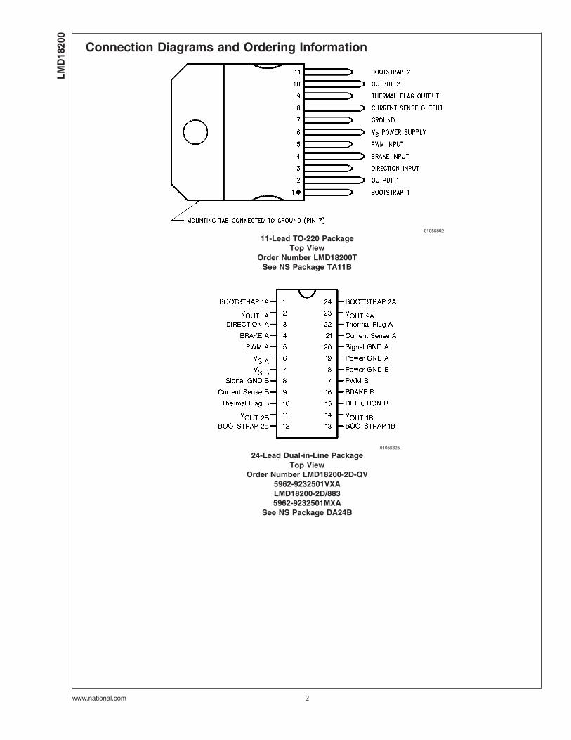
Connection Diagrams and Ordering Information
01056802
11-Lead TO-220 PackageTop View
Order Number LMD18200TSee NS Package TA11B
01056825
24-Lead Dual-in-Line PackageTop View
Order Number LMD18200-2D-QV5962-9232501VXALMD18200-2D/8835962-9232501MXA
See NS Package DA24B
LMD
1820
0
www.national.com 2

Absolute Maximum Ratings (Note 1)
If Military/Aerospace specified devices are required,please contact the National Semiconductor Sales Office/Distributors for availability and specifications.
Total Supply Voltage (VS, Pin 6) 60V
Voltage at Pins 3, 4, 5, 8 and 9 12V
Voltage at Bootstrap Pins
(Pins 1 and 11) VOUT +16V
Peak Output Current (200 ms) 6A
Continuous Output Current (Note 2) 3A
Power Dissipation (Note 3) 25W
Power Dissipation (TA = 25˚C, Free Air) 3W
Junction Temperature, TJ(max) 150˚C
ESD Susceptibility (Note 4) 1500V
Storage Temperature, TSTG −40˚C to+150˚C
Lead Temperature (Soldering, 10 sec.) 300˚C
Operating Ratings(Note 1)
Junction Temperature, TJ −40˚C to +125˚C
VS Supply Voltage +12V to +55V
Electrical Characteristics (Note 5)
The following specifications apply for VS = 42V, unless otherwise specified. Boldface limits apply over the entire operatingtemperature range, −40˚C ≤ TJ ≤ +125˚C, all other limits are for TA = TJ = 25˚C.
Symbol Parameter Conditions Typ Limit Units
RDS(ON) Switch ON Resistance Output Current = 3A (Note 6) 0.33 0.4/0.6 Ω (max)
RDS(ON) Switch ON Resistance Output Current = 6A (Note 6) 0.33 0.4/0.6 Ω (max)
VCLAMP Clamp Diode Forward Drop Clamp Current = 3A (Note 6) 1.2 1.5 V (max)
VIL Logic Low Input Voltage Pins 3, 4, 5 −0.1 V (min)
0.8 V (max)
IIL Logic Low Input Current VIN = −0.1V, Pins = 3, 4, 5 −10 µA (max)
VIH Logic High Input Voltage Pins 3, 4, 5 2 V (min)
12 V (max)
IIH Logic High Input Current VIN = 12V, Pins = 3, 4, 5 10 µA (max)
Current Sense Output IOUT = 1A (Note 8) 377 325/300 µA (min)
425/450 µA (max)
Current Sense Linearity 1A ≤ IOUT ≤ 3A (Note 7) ±6 ±9 %
Undervoltage Lockout Outputs turn OFF 9 V (min)
11 V (max)
TJW Warning Flag Temperature Pin 9 ≤ 0.8V, IL = 2 mA 145 ˚C
VF(ON) Flag Output Saturation Voltage TJ = TJW, IL = 2 mA 0.15 V
IF(OFF) Flag Output Leakage VF = 12V 0.2 10 µA (max)
TJSD Shutdown Temperature Outputs Turn OFF 170 ˚C
IS Quiescent Supply Current All Logic Inputs Low 13 25 mA (max)
tDon Output Turn-On Delay Time Sourcing Outputs, IOUT = 3A 300 ns
Sinking Outputs, IOUT = 3A 300 ns
ton Output Turn-On Switching Time Bootstrap Capacitor = 10 nF
Sourcing Outputs, IOUT = 3A 100 ns
Sinking Outputs, IOUT = 3A 80 ns
tDoff Output Turn-Off Delay Times Sourcing Outputs, IOUT = 3A 200 ns
Sinking Outputs, IOUT = 3A 200 ns
toff Output Turn-Off Switching Times Bootstrap Capacitor = 10 nF
Sourcing Outputs, IOUT = 3A 75 ns
Sinking Outputs, IOUT = 3A 70 ns
tpw Minimum Input Pulse Width Pins 3, 4 and 5 1 µs
tcpr Charge Pump Rise Time No Bootstrap Capacitor 20 µs
LMD
18200
www.national.com3

Electrical Characteristics NotesNote 1: Absolute Maximum Ratings indicate limits beyond which damage to the device may occur. DC and AC electrical specifications do not apply when operatingthe device beyond its rated operating conditions.
Note 2: See Application Information for details regarding current limiting.
Note 3: The maximum power dissipation must be derated at elevated temperatures and is a function of TJ(max), θJA, and TA. The maximum allowable powerdissipation at any temperature is PD(max) = (TJ(max) − TA)/θJA, or the number given in the Absolute Ratings, whichever is lower. The typical thermal resistance fromjunction to case (θJC) is 1.0˚C/W and from junction to ambient (θJA) is 30˚C/W. For guaranteed operation TJ(max) = 125˚C.
Note 4: Human-body model, 100 pF discharged through a 1.5 kΩ resistor. Except Bootstrap pins (pins 1 and 11) which are protected to 1000V of ESD.
Note 5: All limits are 100% production tested at 25˚C. Temperature extreme limits are guaranteed via correlation using accepted SQC (Statistical Quality Control)methods. All limits are used to calculate AOQL, (Average Outgoing Quality Level).
Note 6: Output currents are pulsed (tW < 2 ms, Duty Cycle < 5%).
Note 7: Regulation is calculated relative to the current sense output value with a 1A load.
Note 8: Selections for tighter tolerance are available. Contact factory.
Typical Performance CharacteristicsVSAT vs Flag Current RDS(ON) vs Temperature
01056816 01056817
RDS(ON) vsSupply Voltage
Supply Current vsSupply Voltage
01056818 01056819
LMD
1820
0
www.national.com 4

Typical Performance Characteristics (Continued)
Supply Current vsFrequency (VS = 42V)
Supply Current vsTemperature (VS = 42V)
0105682001056821
Current Sense Outputvs Load Current
Current SenseOperating Region
01056822 01056823
Test Circuit
01056808
LMD
18200
www.national.com5

Switching Time Definitions
01056809
Pinout Description(See Connection Diagram)
Pin 1, BOOTSTRAP 1 Input: Bootstrap capacitor pin for halfH-bridge number 1. The recommended capacitor (10 nF) isconnected between pins 1 and 2.
Pin 2, OUTPUT 1: Half H-bridge number 1 output.
Pin 3, DIRECTION Input: See Table 1. This input controlsthe direction of current flow between OUTPUT 1 and OUT-PUT 2 (pins 2 and 10) and, therefore, the direction of rotationof a motor load.
Pin 4, BRAKE Input: See Table 1. This input is used tobrake a motor by effectively shorting its terminals. Whenbraking is desired, this input is taken to a logic high level andit is also necessary to apply logic high to PWM input, pin 5.The drivers that short the motor are determined by the logiclevel at the DIRECTION input (Pin 3): with Pin 3 logic high,both current sourcing output transistors are ON; with Pin 3logic low, both current sinking output transistors are ON. Alloutput transistors can be turned OFF by applying a logic highto Pin 4 and a logic low to PWM input Pin 5; in this case onlya small bias current (approximately −1.5 mA) exists at eachoutput pin.
Pin 5, PWM Input: See Table 1. How this input (and DIREC-TION input, Pin 3) is used is determined by the format of thePWM Signal.
Pin 6, VS Power Supply
Pin 7, GROUND Connection: This pin is the ground return,and is internally connected to the mounting tab.
Pin 8, CURRENT SENSE Output: This pin provides thesourcing current sensing output signal, which is typically377 µA/A.
Pin 9, THERMAL FLAG Output: This pin provides thethermal warning flag output signal. Pin 9 becomes active-lowat 145˚C (junction temperature). However the chip will notshut itself down until 170˚C is reached at the junction.
Pin 10, OUTPUT 2: Half H-bridge number 2 output.
Pin 11, BOOTSTRAP 2 Input: Bootstrap capacitor pin forHalf H-bridge number 2. The recommended capacitor(10 nF) is connected between pins 10 and 11.
TABLE 1. Logic Truth Table
PWM Dir Brake Active Output Drivers
H H L Source 1, Sink 2
H L L Sink 1, Source 2
L X L Source 1, Source 2
H H H Source 1, Source 2
H L H Sink 1, Sink 2
L X H NONE
Application Information
TYPES OF PWM SIGNALS
The LMD18200 readily interfaces with different forms ofPWM signals. Use of the part with two of the more popularforms of PWM is described in the following paragraphs.
Simple, locked anti-phase PWM consists of a single, vari-able duty-cycle signal in which is encoded both direction andamplitude information (see Figure 2). A 50% duty-cyclePWM signal represents zero drive, since the net value ofvoltage (integrated over one period) delivered to the load iszero. For the LMD18200, the PWM signal drives the direc-tion input (pin 3) and the PWM input (pin 5) is tied to logichigh.
LMD
1820
0
www.national.com 6

Application Information (Continued)
Sign/magnitude PWM consists of separate direction (sign)and amplitude (magnitude) signals (see Figure 3). The (ab-solute) magnitude signal is duty-cycle modulated, and theabsence of a pulse signal (a continuous logic low level)represents zero drive. Current delivered to the load is pro-portional to pulse width. For the LMD18200, the DIRECTIONinput (pin 3) is driven by the sign signal and the PWM input(pin 5) is driven by the magnitude signal.
SIGNAL TRANSITION REQUIREMENTS
To ensure proper internal logic performance, it is good prac-tice to avoid aligning the falling and rising edges of inputsignals. A delay of at least 1 µsec should be incorporatedbetween transitions of the Direction, Brake, and/or PWMinput signals. A conservative approach is be sure there is atleast 500ns delay between the end of the first transition andthe beginning of the second transition. See Figure 4.
01056804
FIGURE 2. Locked Anti-Phase PWM Control
01056805
FIGURE 3. Sign/Magnitude PWM Control
LMD
18200
www.national.com7

Application Information (Continued)
USING THE CURRENT SENSE OUTPUT
The CURRENT SENSE output (pin 8) has a sensitivity of377 µA per ampere of output current. For optimal accuracyand linearity of this signal, the value of voltage generatingresistor between pin 8 and ground should be chosen to limitthe maximum voltage developed at pin 8 to 5V, or less. Themaximum voltage compliance is 12V.
It should be noted that the recirculating currents (free wheel-ing currents) are ignored by the current sense circuitry.Therefore, only the currents in the upper sourcing outputsare sensed.
USING THE THERMAL WARNING FLAG
The THERMAL FLAG output (pin 9) is an open collectortransistor. This permits a wired OR connection of thermalwarning flag outputs from multiple LMD18200’s, and allowsthe user to set the logic high level of the output signal swingto match system requirements. This output typically drivesthe interrupt input of a system controller. The interrupt ser-vice routine would then be designed to take appropriatesteps, such as reducing load currents or initiating an orderlysystem shutdown. The maximum voltage compliance on theflag pin is 12V.
SUPPLY BYPASSING
During switching transitions the levels of fast currentchanges experienced may cause troublesome voltage tran-sients across system stray inductance.
It is normally necessary to bypass the supply rail with a highquality capacitor(s) connected as close as possible to the VS
Power Supply (Pin 6) and GROUND (Pin 7). A 1 µF high-frequency ceramic capacitor is recommended. Care shouldbe taken to limit the transients on the supply pin below theAbsolute Maximum Rating of the device. When operating thechip at supply voltages above 40V a voltage suppressor
(transorb) such as P6KE62A is recommended from supply toground. Typically the ceramic capacitor can be eliminated inthe presence of the voltage suppressor. Note that whendriving high load currents a greater amount of supply bypasscapacitance (in general at least 100 µF per Amp of loadcurrent) is required to absorb the recirculating currents of theinductive loads.
CURRENT LIMITING
Current limiting protection circuitry has been incorporatedinto the design of the LMD18200. With any power device it isimportant to consider the effects of the substantial surgecurrents through the device that may occur as a result ofshorted loads. The protection circuitry monitors this increasein current (the threshold is set to approximately 10 Amps)and shuts off the power device as quickly as possible in theevent of an overload condition. In a typical motor drivingapplication the most common overload faults are caused byshorted motor windings and locked rotors. Under these con-ditions the inductance of the motor (as well as any seriesinductance in the VCC supply line) serves to reduce themagnitude of a current surge to a safe level for theLMD18200. Once the device is shut down, the control cir-cuitry will periodically try to turn the power device back on.This feature allows the immediate return to normal operationin the event that the fault condition has been removed. Whilethe fault remains however, the device will cycle in and out ofthermal shutdown. This can create voltage transients on theVCC supply line and therefore proper supply bypassing tech-niques are required.
The most severe condition for any power device is a direct,hard-wired (“screwdriver”) long term short from an output toground. This condition can generate a surge of currentthrough the power device on the order of 15 Amps andrequire the die and package to dissipate up to 500 Watts ofpower for the short time required for the protection circuitry
01056824
FIGURE 4. Transitions in Brake, Direction, or PWM Must Be Separated By At Least 1 µsec
LMD
1820
0
www.national.com 8

Application Information (Continued)
to shut off the power device. This energy can be destructive,particularly at higher operating voltages (>30V) so someprecautions are in order. Proper heat sink design is essentialand it is normally necessary to heat sink the VCC supply pin(pin 6) with 1 square inch of copper on the PCB.
INTERNAL CHARGE PUMP AND USE OF BOOTSTRAPCAPACITORS
To turn on the high-side (sourcing) DMOS power devices,the gate of each device must be driven approximately 8Vmore positive than the supply voltage. To achieve this aninternal charge pump is used to provide the gate drive volt-age. As shown in Figure 5, an internal capacitor is alternatelyswitched to ground and charged to about 14V, then switchedto V supply thereby providing a gate drive voltage greaterthan V supply. This switching action is controlled by a con-tinuously running internal 300 kHz oscillator. The rise time ofthis drive voltage is typically 20 µs which is suitable foroperating frequencies up to 1 kHz.
For higher switching frequencies, the LMD18200 providesfor the use of external bootstrap capacitors. The bootstrapprinciple is in essence a second charge pump whereby alarge value capacitor is used which has enough energy toquickly charge the parasitic gate input capacitance of thepower device resulting in much faster rise times. The switch-ing action is accomplished by the power switches them-selves Figure 6. External 10 nF capacitors, connected fromthe outputs to the bootstrap pins of each high-side switchprovide typically less than 100 ns rise times allowing switch-ing frequencies up to 500 kHz.
INTERNAL PROTECTION DIODES
A major consideration when switching current through induc-tive loads is protection of the switching power devices fromthe large voltage transients that occur. Each of the fourswitches in the LMD18200 have a built-in protection diode toclamp transient voltages exceeding the positive supply orground to a safe diode voltage drop across the switch.
The reverse recovery characteristics of these diodes, oncethe transient has subsided, is important. These diodes mustcome out of conduction quickly and the power switches mustbe able to conduct the additional reverse recovery current ofthe diodes. The reverse recovery time of the diodes protect-ing the sourcing power devices is typically only 70 ns with areverse recovery current of 1A when tested with a full 6A offorward current through the diode. For the sinking devicesthe recovery time is typically 100 ns with 4A of reversecurrent under the same conditions.
Typical ApplicationsFIXED OFF-TIME CONTROL
This circuit controls the current through the motor by apply-ing an average voltage equal to zero to the motor terminalsfor a fixed period of time, whenever the current through themotor exceeds the commanded current. This action causesthe motor current to vary slightly about an externally con-trolled average level. The duration of the Off-period is ad-justed by the resistor and capacitor combination of theLM555. In this circuit the Sign/Magnitude mode of operationis implemented (see Types of PWM Signals).
01056806
FIGURE 5. Internal Charge Pump Circuitry
01056807
FIGURE 6. Bootstrap Circuitry
LMD
18200
www.national.com9

Typical Applications (Continued)
TORQUE REGULATION
Locked Anti-Phase Control of a brushed DC motor. Currentsense output of the LMD18200 provides load sensing. TheLM3524D is a general purpose PWM controller. The relation-ship of peak motor current to adjustment voltage is shown inFigure 10.
01056810
FIGURE 7. Fixed Off-Time Control
01056811
FIGURE 8. Switching Waveforms
LMD
1820
0
www.national.com 10

Typical Applications (Continued)
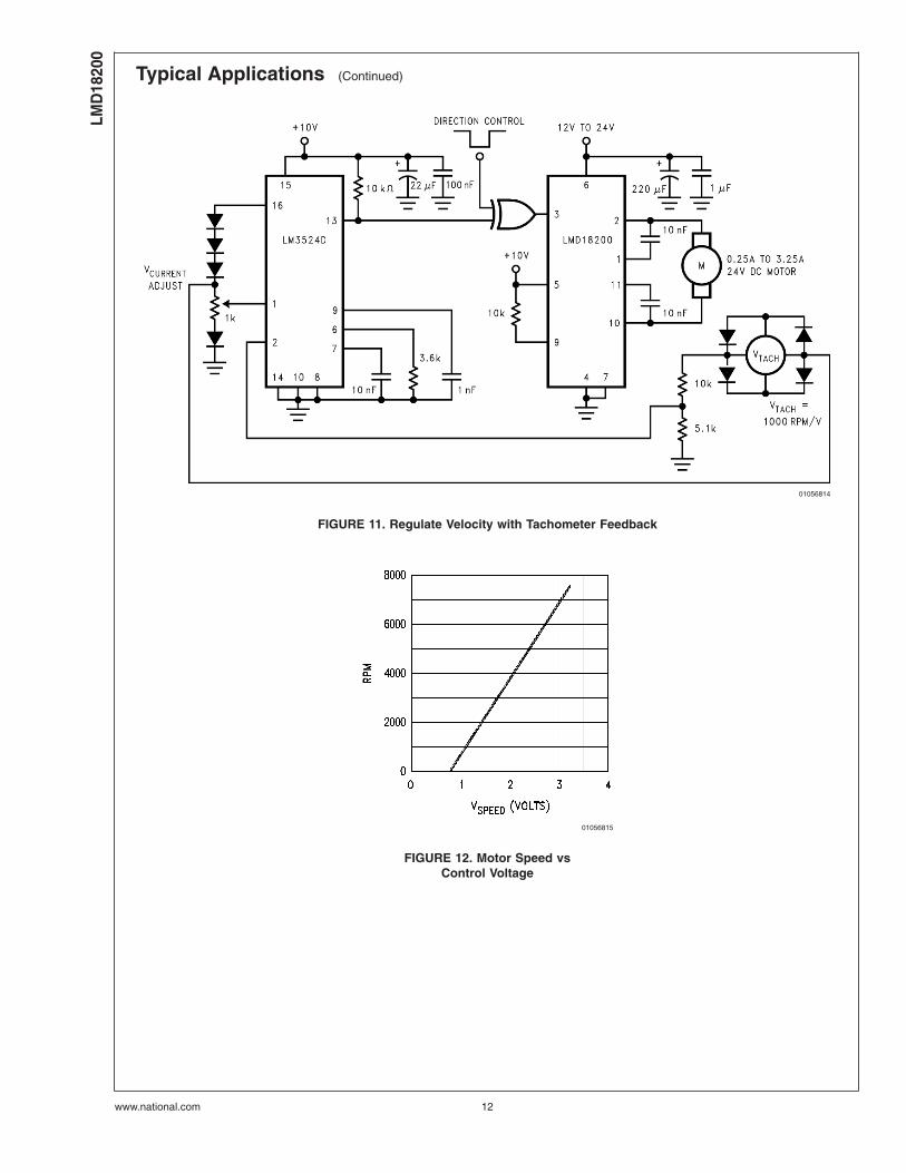
VELOCITY REGULATION
Utilizes tachometer output from the motor to sense motorspeed for a locked anti-phase control loop. The relationshipof motor speed to the speed adjustment control voltage isshown in Figure 12.
01056812
FIGURE 9. Locked Anti-Phase Control Regulates Torque
01056813
FIGURE 10. Peak Motor Currentvs Adjustment Voltage
LMD
18200
www.national.com11
Typical Applications (Continued)
01056814
FIGURE 11. Regulate Velocity with Tachometer Feedback
01056815
FIGURE 12. Motor Speed vsControl Voltage
LMD
1820
0
www.national.com 12
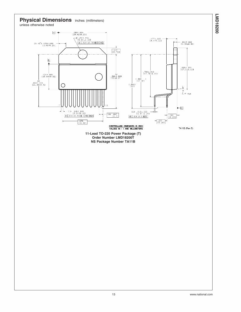
Physical Dimensions inches (millimeters)unless otherwise noted
11-Lead TO-220 Power Package (T)Order Number LMD18200T
NS Package Number TA11B
LMD
18200
www.national.com13
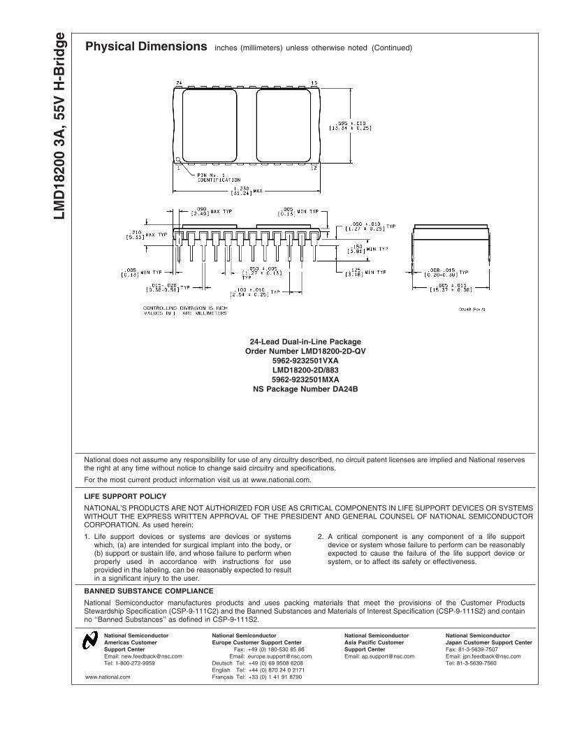
Physical Dimensions inches (millimeters) unless otherwise noted (Continued)
24-Lead Dual-in-Line PackageOrder Number LMD18200-2D-QV
5962-9232501VXALMD18200-2D/8835962-9232501MXA
NS Package Number DA24B
National does not assume any responsibility for use of any circuitry described, no circuit patent licenses are implied and National reservesthe right at any time without notice to change said circuitry and specifications.
For the most current product information visit us at www.national.com.
LIFE SUPPORT POLICY
NATIONAL’S PRODUCTS ARE NOT AUTHORIZED FOR USE AS CRITICAL COMPONENTS IN LIFE SUPPORT DEVICES OR SYSTEMSWITHOUT THE EXPRESS WRITTEN APPROVAL OF THE PRESIDENT AND GENERAL COUNSEL OF NATIONAL SEMICONDUCTORCORPORATION. As used herein:
1. Life support devices or systems are devices or systemswhich, (a) are intended for surgical implant into the body, or(b) support or sustain life, and whose failure to perform whenproperly used in accordance with instructions for useprovided in the labeling, can be reasonably expected to resultin a significant injury to the user.
2. A critical component is any component of a life supportdevice or system whose failure to perform can be reasonablyexpected to cause the failure of the life support device orsystem, or to affect its safety or effectiveness.
BANNED SUBSTANCE COMPLIANCE
National Semiconductor manufactures products and uses packing materials that meet the provisions of the Customer ProductsStewardship Specification (CSP-9-111C2) and the Banned Substances and Materials of Interest Specification (CSP-9-111S2) and containno ‘‘Banned Substances’’ as defined in CSP-9-111S2.
National SemiconductorAmericas CustomerSupport CenterEmail: [email protected]: 1-800-272-9959
National SemiconductorEurope Customer Support Center
Fax: +49 (0) 180-530 85 86Email: [email protected]
Deutsch Tel: +49 (0) 69 9508 6208English Tel: +44 (0) 870 24 0 2171Français Tel: +33 (0) 1 41 91 8790
National SemiconductorAsia Pacific CustomerSupport CenterEmail: [email protected]
National SemiconductorJapan Customer Support CenterFax: 81-3-5639-7507Email: [email protected]: 81-3-5639-7560
www.national.com
LMD
1820
03A
,55V
H-B
ridg
e