Design and implementation of cmos rail to-rail operational amplifiers

LMC7111
www.ti.com SNOS753E –AUGUST 1999–REVISED MARCH 2013
LMC7111 Tiny CMOS Operational Amplifier with Rail-to-Rail Input and OutputCheck for Samples: LMC7111
1FEATURES DESCRIPTIONThe LMC7111 is a micropower CMOS operational
2• Tiny 5-Pin SOT-23 Package Saves Spaceamplifier available in the space saving SOT-23
• Very Wide Common Mode Input Range package. This makes the LMC7111 ideal for space• Specified at 2.7V, 5V, and 10V and weight critical designs. The wide common-mode
input range makes it easy to design battery• Typical Supply Current 25 μA at 5Vmonitoring circuits which sense signals above the V+
• 50 kHz Gain-Bandwidth at 5V supply. The main benefits of the Tiny package are• Similar to Popular LMC6462 most apparent in small portable electronic devices,
such as mobile phones, pagers, and portable• Output to Within 20 mV of Supply Rail at 100kcomputers. The tiny amplifiers can be placed on aLoadboard where they are needed, simplifying board• Good Capacitive Load Drive layout.
APPLICATIONS• Mobile Communications• Portable Computing• Current Sensing for Battery Chargers• Voltage Reference Buffering• Sensor Interface• Stable Bias for GaAs RF Amps
Connection Diagram
Figure 1. 8-Pin PDIP Figure 2. 5-Pin SOT-23Top View Top View
Figure 3. Actual Size
1
Please be aware that an important notice concerning availability, standard warranty, and use in critical applications ofTexas Instruments semiconductor products and disclaimers thereto appears at the end of this data sheet.
2All trademarks are the property of their respective owners.
PRODUCTION DATA information is current as of publication date. Copyright © 1999–2013, Texas Instruments IncorporatedProducts conform to specifications per the terms of the TexasInstruments standard warranty. Production processing does notnecessarily include testing of all parameters.

LMC7111
SNOS753E –AUGUST 1999–REVISED MARCH 2013 www.ti.com
These devices have limited built-in ESD protection. The leads should be shorted together or the device placed in conductive foamduring storage or handling to prevent electrostatic damage to the MOS gates.
Absolute Maximum Ratings (1) (2)
ESD Tolerance (3) SOT-23 Package 2000V
PDIP Package 1500V
Differential Input Voltage ±Supply Voltage
Voltage at Input/Output Pin (V+) + 0.3V, (V−) − 0.3V
Supply Voltage (V+ − V−) 11V
Current at Input Pin ±5 mA
Current at Output Pin (4) ±30 mA
Current at Power Supply Pin 30 mA
Lead Temp. (Soldering, 10 sec.) 260°C
Storage Temperature Range −65°C to +150°C
Junction Temperature (5) 150°C
(1) Absolute Maximum Ratings indicate limits beyond which damage to the device may occur. Operating Ratings indicate conditions forwhich the device is intended to be functional, but specific performance is not ensured. For ensured specifications and the testconditions, see the Electrical Characteristics.
(2) If Military/Aerospace specified devices are required, please contact the TI Sales Office/ Distributors for availability and specifications.(3) Human Body Model is 1.5 kΩ in series with 100 pF.(4) Applies to both single-supply and split-supply operation. Continuous short circuit operation at elevated ambient temperature can result in
exceeding the maximum allowed junction temperature at 150°C.(5) The maximum power dissipation is a function of TJ(MAX), θJA and TA. The maximum allowable power dissipation at any ambient
temperature is PD = (TJ(MAX) − TA)/θJA. All numbers apply for packages soldered directly into a PC board.
Operating Ratings (1)
Supply Voltage 2.5V ≤ V+ ≤ 11V
Junction Temperature Range LMC7111AI, LMC7111BI −40°C ≤ TJ ≤ +85°C
Thermal Resistance (θJA) 8-Pin PDIP 115°C/W
5-Pin SOT-23 325°C/W
(1) Absolute Maximum Ratings indicate limits beyond which damage to the device may occur. Operating Ratings indicate conditions forwhich the device is intended to be functional, but specific performance is not specified. For ensured specifications and the testconditions, see the Electrical Characteristics.
2.7V DC Electrical CharacteristicsUnless otherwise specified, all limits specified for TJ = 25°C, V+ = 2.7V, V− = 0V, VCM = VO = V+/2 and RL > 1 MΩ. Boldfacelimits apply at the temperature extremes.
Symbol Parameter Conditions LMC7111AI LMC7111BI UnitsTyp (1)Limit (2) Limit (2)
VOS Input Offset Voltage V+ = 2.7V 0.9 3 7 mV
5 9 max
TCVOS Input Offset Voltage 2.0 μV/°CAverage Drift
IB Input Bias Current See (3) 0.1 1 1 pA20 20 max
IOS Input Offset Current See (3) 0.01 0.5 0.5 pA10 10 max
RIN Input Resistance >10 Tera Ω+PSRR Positive Power Supply 2.7V ≤ V+ ≤5.0V, 60 55 55 dB
Rejection Ratio V− = 0V, VO = 2.5V 50 50 min
−PSRR Negative Power Supply −2.7V ≤ V− ≤−5.0V, 60 55 55 dBRejection Ratio V− = 0V, VO = 2.5V 50 50 min
(1) Typical Values represent the most likely parametric norm.(2) All limits are specified by testing or statistical analysis.(3) Bias Current specified by design and processing.
2 Submit Documentation Feedback Copyright © 1999–2013, Texas Instruments Incorporated
Product Folder Links: LMC7111

LMC7111
www.ti.com SNOS753E –AUGUST 1999–REVISED MARCH 2013
2.7V DC Electrical Characteristics (continued)Unless otherwise specified, all limits specified for TJ = 25°C, V+ = 2.7V, V− = 0V, VCM = VO = V+/2 and RL > 1 MΩ. Boldfacelimits apply at the temperature extremes.
Symbol Parameter Conditions LMC7111AI LMC7111BI UnitsTyp (1)Limit (2) Limit (2)
VCM Input Common-Mode V+ = 2.7V −0.10 0.0 0.0 VVoltage Range For CMRR ≥ 50 dB 0.40 0.40 min
2.8 2.7 2.7 V2.25 2.25 max
CIN Common-Mode Input 3 pFCapacitance
VO Output Swing V+ = 2.7V 2.69 2.68 2.68 VRL = 100 kΩ 2.4 2.4 min
0.01 0.02 0.02 V0.08 0.08 max
V+ = 2.7V 2.65 2.6 2.6 VRL = 10 kΩ 2.4 2.4 min
0.03 0.1 0.1 V0.3 0.3 max
ISC Output Short Circuit Current Sourcing, VO = 0V 7 1 1 mA0.7 0.7 min
Sinking, VO = 2.7V 7 1 1 mA0.7 0.7 min
AVOL Voltage Gain Sourcing 400 V/mvmin
Sinking 150 V/mvmin
IS Supply Current V+ = +2.7V, 20 45 50 μAVO = V+/2 60 65 max
2.7V AC Electrical CharacteristicsUnless otherwise specified, all limits specified for TJ = 25°C, V+ = 2.7V, V− = 0V, VCM = VO = V+/2 and RL > 1 MΩ. Boldfacelimits apply at the temperature extremes.
Symbol Parameter Conditions LMC7111AI LMC7111BI UnitsTyp (1)Limit (2) Limit (2)
SR Slew Rate See (3) 0.015 V/μs
GBW Gain-Bandwidth Product 40 kHz
(1) Typical Values represent the most likely parametric norm.(2) All limits are specified by testing or statistical analysis.(3) Connected as Voltage Follower with 1.0V step input. Number specified is the slower of the positive and negative slew rates. Input
referred, V+ = 2.7V and RL = 100 kΩ connected to 1.35V. Amp excited with 1 kHz to produce VO = 1 VPP.
3V DC Electrical CharacteristicsUnless otherwise specified, all limits specified for TJ = 25°C, V+ = 3V, V− = 0V, VCM = VO = V+/2 and RL > 1 MΩ. Boldfacelimits apply at the temperature extremes.
Symbol Parameter Conditions LMC7111AI LMC7111BI UnitsTyp (1)Limit (2) Limit (2)
VCM Input Common-Mode V+ = 3V −0.25 0.0 0.0 VVoltage Range For CMRR ≥ 50 dB min
3.2 3.0 3.0 V2.8 2.8 max
(1) Typical Values represent the most likely parametric norm.(2) All limits are specified by testing or statistical analysis.
Copyright © 1999–2013, Texas Instruments Incorporated Submit Documentation Feedback 3
Product Folder Links: LMC7111

LMC7111
SNOS753E –AUGUST 1999–REVISED MARCH 2013 www.ti.com
3.3V DC Electrical CharacteristicsUnless otherwise specified, all limits specified for TJ = 25°C, V+ = 3.3V, V− = 0V, VCM = VO = V+/2 and RL > 1 MΩ. Boldfacelimits apply at the temperature extremes.
Symbol Parameter Conditions LMC7111AI LMC7111BI UnitsTyp (1)Limit (2) Limit (2)
VCM Input Common-Mode V+ = 3.3V −0.25 −0.1 −0.1 VVoltage Range For CMRR ≥ 50 dB 0.00 0.00 min
3.5 3.4 3.4 V3.2 3.2 max
(1) Typical Values represent the most likely parametric norm.(2) All limits are specified by testing or statistical analysis.
5V DC Electrical CharacteristicsUnless otherwise specified, all limits specified for TJ = 25°C, V+ = 5V, V− = 0V, VCM = VO = V+/2 and RL > 1 MΩ. Boldfacelimits apply at the temperature extremes.
Symbol Parameter Conditions LMC7111AI LMC7111BI UnitsTyp (1)Limit (2) Limit (2)
VOS Input Offset Voltage V+ = 5V 0.9 mVmax
TCVOS Input Offset Voltage 2.0 μV/°CAverage Drift
IB Input Bias Current See (3) 0.1 1 1 pA20 20 max
IOS Input Offset Current See (3) 0.01 0.5 0.5 pA10 10 max
RIN Input Resistance >10 Tera ΩCMRR Common Mode 0V ≤ VCM ≤ 5V 85 70 60 dB
Rejection Ratio min
+PSRR Positive Power Supply 5V ≤ V+ ≤10V, 85 70 60 dBRejection Ratio V− = 0V, VO = 2.5V min
−PSRR Negative Power Supply −5V ≤ V− ≤−10V, 85 70 60 dBRejection Ratio V− = 0V, VO = −2.5V min
VCM Input Common-Mode V+ = 5V −0.3 −0.20 −0.20 VVoltage Range For CMRR ≥ 50 dB 0.00 0.00 min
5.25 5.20 5.20 V5.00 5.00 max
CIN Common-Mode Input 3 pFCapacitance
VO Output Swing V+ = 5V 4.99 4.98 4.98 VminRL = 100 kΩ 0.01 0.02 0.02 Vmax
V+ = 5V 4.98 4.9 4.9 VminRL = 10 kΩ 0.02 0.1 0.1 Vmin
ISC Output Short Circuit Current Sourcing, VO = 0V 7 5 5 mA3.5 3.5 min
Sinking, VO = 3V 7 5 5 mA3.5 3.5 min
AVOL Voltage Gain Sourcing 500 V/mvmin
Sinking 200 V/mvmin
IS Supply Current V+ = +5V, 25 μAVO = V+/2 max
(1) Typical Values represent the most likely parametric norm.(2) All limits are specified by testing or statistical analysis.(3) Bias Current specified by design and processing.
4 Submit Documentation Feedback Copyright © 1999–2013, Texas Instruments Incorporated
Product Folder Links: LMC7111

LMC7111
www.ti.com SNOS753E –AUGUST 1999–REVISED MARCH 2013
5V AC Electrical CharacteristicsUnless otherwise specified, all limits specified for TJ = 25°C, V+ = 5V, V− = 0V, VCM = VO = V+/2 and RL > 1 MΩ. Boldfacelimits apply at the temperature extremes.
Symbol Parameter Conditions LMC7111AI LMC7111BI UnitsTyp (1)Limit (2) Limit (2)
SR Slew Rate Positive Going Slew Rate (3) 0.027 0.015 0.010 V/μs
GBW Gain-Bandwidth Product 50 kHz
(1) Typical Values represent the most likely parametric norm.(2) All limits are specified by testing or statistical analysis.(3) Connected as Voltage Follower with 1.0V step input. Number specified is the slower of the positive slew rate. The negative slew rate is
faster. Input referred, V+ = 5V and RL = 100 kΩ connected to 1.5V. Amp excited with 1 kHz to produce VO = 1 VPP.
10V DC Electrical CharacteristicsUnless otherwise specified, all limits specified for TJ = 25°C, V+ = 10V, V− = 0V, VCM = VO = V+/2 and RL > 1 MΩ. Boldfacelimits apply at the temperature extremes.
Symbol Parameter Conditions LMC7111AI LMC7111BI UnitsTyp (1)Limit (2) Limit (2)
VOS Input Offset Voltage V+ = 10V 0.9 3 7 mV5 9 max
TCVOS Input Offset Voltage 2.0 μV/°CAverage Drift
IB Input Bias Current 0.1 1 1 pA20 20 max
IOS Input Offset Current 0.01 0.5 0.5 pA10 10 max
RIN Input Resistance >10 Tera Ω+PSRR Positive Power Supply 5V ≤ V+ ≤10V, 80 dB
Rejection Ratio V− = 0V, VO = 2.5V min
−PSRR Negative Power Supply −5V ≤ V− ≤−10V, 80 dBRejection Ratio V− = 0V, VO = 2.5V min
VCM Input Common-Mode V+ = 10V −0.2 −0.15 −0.15 VVoltage Range For CMRR ≥ 50 dB 0.00 0.00 min
10.2 10.15 10.15 V10.00 10.00 max
CIN Common-Mode Input 3 pFCapacitance
ISC Output Short Circuit Current (3) Sourcing, VO = 0V 30 20 20 mA7 7 min
Sinking, VO = 10V 30 20 20 mA7 7 min
AVOL Voltage Gain Sourcing 500 V/mv100 kΩ Load min
Sinking 200 V/mvmin
IS Supply Current V+ = +10V, 25 50 60 μAVO = V+/2 65 75 max
VO Output Swing V+ = 10V 9.99 9.98 9.98 VminRL = 100 kΩ 0.01 0.02 0.02 Vmax
V+ = 10V 9.98 9.9 9.9 VminRL = 10 kΩ 0.02 0.1 0.1 Vmin
(1) Typical Values represent the most likely parametric norm.(2) All limits are specified by testing or statistical analysis.(3) Bias Current specified by design and processing.
Copyright © 1999–2013, Texas Instruments Incorporated Submit Documentation Feedback 5
Product Folder Links: LMC7111

LMC7111
SNOS753E –AUGUST 1999–REVISED MARCH 2013 www.ti.com
10V AC Electrical CharacteristicsUnless otherwise specified, all limits specified for TJ = 25°C, V+ = 10V, V− = 0V, VCM = VO = V+/2 and RL > 1 MΩ. Boldfacelimits apply at the temperature extremes.
Symbol Parameter Conditions LMC7111AI LMC7111BI UnitsTyp (1)Limit (2) Limit (2)
SR Slew Rate See (3) 0.03 V/μs
GBW Gain-Bandwidth Product 50 kHz
φm Phase Margin 50 deg
Gm Gain Margin 15 dB
Input-Referred f = 1 kHz 110 nV/ √HzVoltage Noise VCM = 1V
Input-Referred f = 1 kHz 0.03 pA/√HzCurrent Noise
(1) Typical Values represent the most likely parametric norm.(2) All limits are specified by testing or statistical analysis.(3) Connected as Voltage Follower with 1.0V step input. Number specified is the slower of the positive and negative slew rates. Input
referred, V+ = 10V and RL = 100 kΩ connected to 5V. Amp excited with 1 kHz to produce VO = 2 VPP.
6 Submit Documentation Feedback Copyright © 1999–2013, Texas Instruments Incorporated
Product Folder Links: LMC7111

LMC7111
www.ti.com SNOS753E –AUGUST 1999–REVISED MARCH 2013
Typical Performance CharacteristicsTA = 25°C unless specified, Single Supply
Supply Current Voltage Noisevs. vs.
Supply Voltage Frequency
Figure 4. Figure 5.
2.7V Performance
Offset Voltage Sinking Outputvs. vs.
Common Mode Voltage @ 2.7V Output Voltage
Figure 6. Figure 7.
Sourcing Output Gain and Phasevs. vs.
Output Voltage Capacitive Load @ 2.7V
Figure 8. Figure 9.
Copyright © 1999–2013, Texas Instruments Incorporated Submit Documentation Feedback 7
Product Folder Links: LMC7111

LMC7111
SNOS753E –AUGUST 1999–REVISED MARCH 2013 www.ti.com
2.7V Performance (continued)
Gain and Phase Gain and Phasevs. vs.
Capacitive Load @ 2.7V Capacitive Load @ 2.7V
Figure 10. Figure 11.
3V Performance
Voltage Noise Output Voltagevs. vs.
Common Mode Voltage @ 3V Input Voltage @ 3V
Figure 12. Figure 13.
Offset Voltage Sourcing Outputvs. vs.
Common Mode Voltage @ 3V Output Voltage
Figure 14. Figure 15.
8 Submit Documentation Feedback Copyright © 1999–2013, Texas Instruments Incorporated
Product Folder Links: LMC7111

LMC7111
www.ti.com SNOS753E –AUGUST 1999–REVISED MARCH 2013
3V Performance (continued)Sinking Output Gain and Phase
vs. vs.Output Voltage Capacitive Load @ 3V
Figure 16. Figure 17.
Gain and Phase Gain and Phasevs. vs.
Capacitive Load @ 3V Capacitive Load @ 3V
Figure 18. Figure 19.
5V Performance
Voltage Noise Output Voltagevs. vs.
Common Mode Voltage @ 5V Input Voltage @ 5V
Figure 20. Figure 21.
Copyright © 1999–2013, Texas Instruments Incorporated Submit Documentation Feedback 9
Product Folder Links: LMC7111

LMC7111
SNOS753E –AUGUST 1999–REVISED MARCH 2013 www.ti.com
5V Performance (continued)Offset Voltage Sourcing Output
vs. vs.Common Mode Voltage @ 5V Output Voltage
Figure 22. Figure 23.
Sinking Output Gain and Phasevs. vs.
Output Voltage Capacitive Load @ 5V
Figure 24. Figure 25.
Gain and Phase Gain and Phasevs. vs.
Capacitive Load @ 5V Capacitive Load @ 5V
Figure 26. Figure 27.
10 Submit Documentation Feedback Copyright © 1999–2013, Texas Instruments Incorporated
Product Folder Links: LMC7111

LMC7111
www.ti.com SNOS753E –AUGUST 1999–REVISED MARCH 2013
5V Performance (continued)Non-Inverting Non-Inverting
Small Signal Pulse Response Small Signal Pulse Responseat 5V at 5V
Figure 28. Figure 29.
Non-Inverting Non-InvertingSmall Signal Pulse Response Large Signal Pulse Response
at 5V at 5V
Figure 30. Figure 31.
Non-Inverting Non-InvertingLarge Signal Pulse Response Large Signal Pulse Response
at 5V at 5V
Figure 32. Figure 33.
Copyright © 1999–2013, Texas Instruments Incorporated Submit Documentation Feedback 11
Product Folder Links: LMC7111

LMC7111
SNOS753E –AUGUST 1999–REVISED MARCH 2013 www.ti.com
5V Performance (continued)Inverting Inverting
Small Signal Pulse Response Small Signal Pulse Responseat 5V at 5V
Figure 34. Figure 35.
Inverting InvertingSmall Signal Pulse Response Large Signal Pulse Response
at 5V at 5V
Figure 36. Figure 37.
Inverting InvertingLarge Signal Pulse Response Large Signal Pulse Response
at 5V at 5V
Figure 38. Figure 39.
12 Submit Documentation Feedback Copyright © 1999–2013, Texas Instruments Incorporated
Product Folder Links: LMC7111
LMC7111
www.ti.com SNOS753E –AUGUST 1999–REVISED MARCH 2013
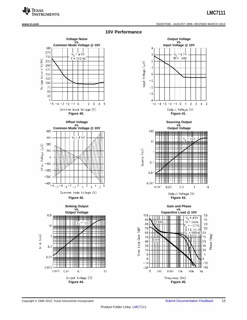
10V Performance
Voltage Noise Output Voltagevs. vs.
Common Mode Voltage @ 10V Input Voltage @ 10V
Figure 40. Figure 41.
Offset Voltage Sourcing Outputvs. vs.
Common Mode Voltage @ 10V Output Voltage
Figure 42. Figure 43.
Sinking Output Gain and Phasevs. vs.
Output Voltage Capacitive Load @ 10V
Figure 44. Figure 45.
Copyright © 1999–2013, Texas Instruments Incorporated Submit Documentation Feedback 13
Product Folder Links: LMC7111

LMC7111
SNOS753E –AUGUST 1999–REVISED MARCH 2013 www.ti.com
10V Performance (continued)Gain and Phase Gain and Phase
vs. vs.Capacitive Load @ 10V Capacitive Load @ 10V
Figure 46. Figure 47.
Non-Inverting Non-InvertingSmall Signal Pulse Response Large Signal Pulse Response
at 10V at 10V
Figure 48. Figure 49.
Inverting InvertingSmall Signal Pulse Response Large Signal Pulse Response
at 10V at 10V
Figure 50. Figure 51.
14 Submit Documentation Feedback Copyright © 1999–2013, Texas Instruments Incorporated
Product Folder Links: LMC7111

LMC7111
www.ti.com SNOS753E –AUGUST 1999–REVISED MARCH 2013
APPLICATION INFORMATION
BENEFITS OF THE LMC7111 TINY AMP
Size
The small footprint of the SOT-23 packaged Tiny amp, (0.120 x 0.118 inches, 3.05 x 3.00 mm) saves space onprinted circuit boards, and enable the design of smaller electronic products. Because they are easier to carry,many customers prefer smaller and lighter products.
Height
The height (0.056 inches, 1.43 mm) of the Tiny amp makes it possible to use it in PCMCIA type III cards.
Signal Integrity
Signals can pick up noise between the signal source and the amplifier. By using a physically smaller amplifierpackage, the Tiny amp can be placed closer to the signal source, reducing noise pickup and increasing signalintegrity. The Tiny amp can also be placed next to the signal destination, such as a buffer for the reference of ananalog to digital converter.
Simplified Board Layout
The Tiny amp can simplify board layout in several ways. First, by placing an amp where amps are needed,instead of routing signals to a dual or quad device, long pc traces may be avoided.
By using multiple Tiny amps instead of duals or quads, complex signal routing and possibly crosstalk can bereduced.
DIPs available for prototyping
LMC7111 amplifiers packaged in conventional 8-pin dip packages can be used for prototyping and evaluationwithout the need to use surface mounting in early project stages.
Low Supply Current
The typical 25 μA supply current of the LMC7111 extends battery life in portable applications, and may allow thereduction of the size of batteries in some applications.
Wide Voltage Range
The LMC7111 is characterized at 2.7V, 3V, 3.3V, 5V and 10V. Performance data is provided at these popularvoltages. This wide voltage range makes the LMC7111 a good choice for devices where the voltage may varyover the life of the batteries.
INPUT COMMON MODE VOLTAGE RANGE
The LMC7111 does not exhibit phase inversion when an input voltage exceeds the negative supply voltage.
The absolute maximum input voltage is 300 mV beyond either rail at room temperature. Voltages greatlyexceeding this maximum rating can cause excessive current to flow in or out of the input pins, adversely affectingreliability.
Applications that exceed this rating must externally limit the maximum input current to ±5 mA with an inputresistor as shown in Figure 52.
Figure 52. RI Input Current Protection forVoltages Exceeding the Supply Voltage
Copyright © 1999–2013, Texas Instruments Incorporated Submit Documentation Feedback 15
Product Folder Links: LMC7111

LMC7111
SNOS753E –AUGUST 1999–REVISED MARCH 2013 www.ti.com
CAPACITIVE LOAD TOLERANCE
The LMC7111 can typically directly drive a 300 pF load with VS = 10V at unity gain without oscillating. The unitygain follower is the most sensitive configuration. Direct capacitive loading reduces the phase margin of op-amps.The combination of the op-amp's output impedance and the capacitive load induces phase lag. This results ineither an underdamped pulse response or oscillation.
Capacitive load compensation can be accomplished using resistive isolation as shown in Figure 53. This simpletechnique is useful for isolating the capacitive input of multiplexers and A/D converters.
Figure 53. Resistive Isolationof a 330 pF Capacitive Load
COMPENSATING FOR INPUT CAPACITANCE WHEN USING LARGE VALUE FEEDBACKRESISTORS
When using very large value feedback resistors, (usually > 500 kΩ) the large feed back resistance can react withthe input capacitance due to transducers, photodiodes, and circuit board parasitics to reduce phase margins.
The effect of input capacitance can be compensated for by adding a feedback capacitor. The feedback capacitor(as in Figure 54), Cf is first estimated by:
(1)
orR1 CIN ≤ R2 Cf (2)
which typically provides significant overcompensation.
Printed circuit board stray capacitance may be larger or smaller than that of a breadboard, so the actual optimumvalue for CF may be different. The values of CF should be checked on the actual circuit. (Refer to the LMC660quad CMOS amplifier data sheet for a more detailed discussion.)
Figure 54. Cancelling the Effect of Input Capacitance
OUTPUT SWING
The output of the LMC7111 will go to within 100 mV of either power supply rail for a 10 kΩ load and to 20 mV ofthe rail for a 100 kΩ load. This makes the LMC7111 useful for driving transistors which are connected to thesame power supply. By going very close to the supply, the LMC7111 can turn the transistors all the way on or allthe way off.
16 Submit Documentation Feedback Copyright © 1999–2013, Texas Instruments Incorporated
Product Folder Links: LMC7111

LMC7111
www.ti.com SNOS753E –AUGUST 1999–REVISED MARCH 2013
BIASING GaAs RF AMPLIFIERS
The capacitive load capability, low current draw, and small size of the SOT-23 LMC7111 make it a good choicefor providing a stable negative bias to other integrated circuits.
The very small size of the LMC7111 and the LM4040 reference take up very little board space.
CF and Risolation prevent oscillations when driving capacitive loads.
Figure 55. Stable Negative Bias
REFERENCE BUFFER FOR A-TO-D CONVERTERS
The LMC7111 can be used as a voltage reference buffer for analog-to-digital converters. This works best for A-to-D converters whose reference input is a static load, such as dual slope integrating A-to-Ds. Converters whosereference input is a dynamic load (the reference current changes with time) may need a faster device, such asthe LMC7101 or the LMC7131.
The small size of the LMC7111 allows it to be placed close to the reference input. The low supply current (25 μAtypical) saves power.
For A-to-D reference inputs which require higher accuracy and lower offset voltage, please see the LMC6462datasheet. The LMC6462 has performance similar to the LMC7111. The LMC6462 is available in two grades withreduced input voltage offset.
DUAL AND QUAD DEVICES WITH SIMILAR PERFORMANCE
The LMC6462 and LMC6464 are dual and quad devices with performance similar to the LMC7111. They areavailable in both conventional through-hole and surface mount packaging. Please see the LMC6462/4 datasheetfor details.
SPICE MACROMODEL
A SPICE macromodel is available for the LMC7111. This model includes simulation of:• Input common-mode voltage range• Frequency and transient response
Copyright © 1999–2013, Texas Instruments Incorporated Submit Documentation Feedback 17
Product Folder Links: LMC7111

LMC7111
SNOS753E –AUGUST 1999–REVISED MARCH 2013 www.ti.com
• Quiescent and dynamic supply current• Output swing dependence on loading conditions and many more characteristics as listed on the macro model
disk. Visit the LMC7111 product page on http://www.ti.com for the spice model.
ADDITIONAL SOT-23 TINY DEVICES
Additional parts are available in the space saving SOT-23 Tiny package, including amplifiers, voltage references,and voltage regulators. These devices include—
LMC7101 1 MHz gain-bandwidth rail-to-rail input and output amplifier—high input impedance and high gain, 700μA typical current 2.7V, 3V, 5V and 15V specifications.
LM7131 Tiny Video amp with 70 MHz gain bandwidth. Specified at 3V, 5V and ± 5V supplies.
LMC7211 Comparator in a tiny package with rail-to-rail input and push-pull output. Typical supply current of 7μA. Typical propagation delay of 7 μs. Specified at 2.7V, 5V and 15V supplies.
LMC7221 Comparator with an open drain output for use in mixed voltage systems. Similar to the LMC7211,except the output can be used with a pull-up resistor to a voltage different than the supply voltage.
LP2980 Micropower SOT 50 mA Ultra Low-Dropout Regulator.
LM4040 Precision micropower shunt voltage reference. Fixed voltages of 2.5000V, 4.096V, 5.000V, 8.192V and10.000V.
LM4041 Precision micropower shunt voltage reference 1.225V and adjustable.
Visit http://www.ti.com for more information.
18 Submit Documentation Feedback Copyright © 1999–2013, Texas Instruments Incorporated
Product Folder Links: LMC7111

LMC7111
www.ti.com SNOS753E –AUGUST 1999–REVISED MARCH 2013
REVISION HISTORY
Changes from Revision D (March 2013) to Revision E Page
• Changed layout of National Data Sheet to TI format .......................................................................................................... 18
Copyright © 1999–2013, Texas Instruments Incorporated Submit Documentation Feedback 19
Product Folder Links: LMC7111

PACKAGE OPTION ADDENDUM
www.ti.com 1-Nov-2013
Addendum-Page 1
PACKAGING INFORMATION
Orderable Device Status(1)
Package Type PackageDrawing
Pins PackageQty
Eco Plan(2)
Lead/Ball Finish(6)
MSL Peak Temp(3)
Op Temp (°C) Device Marking(4/5)
Samples
LMC7111BIM5 NRND SOT-23 DBV 5 1000 TBD Call TI Call TI -40 to 85 A01B
LMC7111BIM5/NOPB ACTIVE SOT-23 DBV 5 1000 Green (RoHS& no Sb/Br)
CU SN Level-1-260C-UNLIM -40 to 85 A01B
LMC7111BIM5X NRND SOT-23 DBV 5 3000 TBD Call TI Call TI -40 to 85 A01B
LMC7111BIM5X/NOPB ACTIVE SOT-23 DBV 5 3000 Green (RoHS& no Sb/Br)
CU SN Level-1-260C-UNLIM -40 to 85 A01B
(1) The marketing status values are defined as follows:ACTIVE: Product device recommended for new designs.LIFEBUY: TI has announced that the device will be discontinued, and a lifetime-buy period is in effect.NRND: Not recommended for new designs. Device is in production to support existing customers, but TI does not recommend using this part in a new design.PREVIEW: Device has been announced but is not in production. Samples may or may not be available.OBSOLETE: TI has discontinued the production of the device.
(2) Eco Plan - The planned eco-friendly classification: Pb-Free (RoHS), Pb-Free (RoHS Exempt), or Green (RoHS & no Sb/Br) - please check http://www.ti.com/productcontent for the latest availabilityinformation and additional product content details.TBD: The Pb-Free/Green conversion plan has not been defined.Pb-Free (RoHS): TI's terms "Lead-Free" or "Pb-Free" mean semiconductor products that are compatible with the current RoHS requirements for all 6 substances, including the requirement thatlead not exceed 0.1% by weight in homogeneous materials. Where designed to be soldered at high temperatures, TI Pb-Free products are suitable for use in specified lead-free processes.Pb-Free (RoHS Exempt): This component has a RoHS exemption for either 1) lead-based flip-chip solder bumps used between the die and package, or 2) lead-based die adhesive used betweenthe die and leadframe. The component is otherwise considered Pb-Free (RoHS compatible) as defined above.Green (RoHS & no Sb/Br): TI defines "Green" to mean Pb-Free (RoHS compatible), and free of Bromine (Br) and Antimony (Sb) based flame retardants (Br or Sb do not exceed 0.1% by weightin homogeneous material)
(3) MSL, Peak Temp. - The Moisture Sensitivity Level rating according to the JEDEC industry standard classifications, and peak solder temperature.
(4) There may be additional marking, which relates to the logo, the lot trace code information, or the environmental category on the device.
(5) Multiple Device Markings will be inside parentheses. Only one Device Marking contained in parentheses and separated by a "~" will appear on a device. If a line is indented then it is a continuationof the previous line and the two combined represent the entire Device Marking for that device.
(6) Lead/Ball Finish - Orderable Devices may have multiple material finish options. Finish options are separated by a vertical ruled line. Lead/Ball Finish values may wrap to two lines if the finishvalue exceeds the maximum column width.
Important Information and Disclaimer:The information provided on this page represents TI's knowledge and belief as of the date that it is provided. TI bases its knowledge and belief on informationprovided by third parties, and makes no representation or warranty as to the accuracy of such information. Efforts are underway to better integrate information from third parties. TI has taken and

PACKAGE OPTION ADDENDUM
www.ti.com 1-Nov-2013
Addendum-Page 2
continues to take reasonable steps to provide representative and accurate information but may not have conducted destructive testing or chemical analysis on incoming materials and chemicals.TI and TI suppliers consider certain information to be proprietary, and thus CAS numbers and other limited information may not be available for release.
In no event shall TI's liability arising out of such information exceed the total purchase price of the TI part(s) at issue in this document sold by TI to Customer on an annual basis.

TAPE AND REEL INFORMATION
*All dimensions are nominal
Device PackageType
PackageDrawing
Pins SPQ ReelDiameter
(mm)
ReelWidth
W1 (mm)
A0(mm)
B0(mm)
K0(mm)
P1(mm)
W(mm)
Pin1Quadrant
LMC7111BIM5 SOT-23 DBV 5 1000 178.0 8.4 3.2 3.2 1.4 4.0 8.0 Q3
LMC7111BIM5/NOPB SOT-23 DBV 5 1000 178.0 8.4 3.2 3.2 1.4 4.0 8.0 Q3
LMC7111BIM5X SOT-23 DBV 5 3000 178.0 8.4 3.2 3.2 1.4 4.0 8.0 Q3
LMC7111BIM5X/NOPB SOT-23 DBV 5 3000 178.0 8.4 3.2 3.2 1.4 4.0 8.0 Q3
PACKAGE MATERIALS INFORMATION
www.ti.com 20-Dec-2016
Pack Materials-Page 1

*All dimensions are nominal
Device Package Type Package Drawing Pins SPQ Length (mm) Width (mm) Height (mm)
LMC7111BIM5 SOT-23 DBV 5 1000 210.0 185.0 35.0
LMC7111BIM5/NOPB SOT-23 DBV 5 1000 210.0 185.0 35.0
LMC7111BIM5X SOT-23 DBV 5 3000 210.0 185.0 35.0
LMC7111BIM5X/NOPB SOT-23 DBV 5 3000 210.0 185.0 35.0
PACKAGE MATERIALS INFORMATION
www.ti.com 20-Dec-2016
Pack Materials-Page 2


www.ti.com
PACKAGE OUTLINE
C
TYP0.220.08
0.25
3.02.6
2X 0.95
1.9
1.45 MAX
TYP0.150.00
5X 0.50.3
TYP0.60.3
TYP80
1.9
A
3.052.75
B1.751.45
(1.1)
SOT-23 - 1.45 mm max heightDBV0005ASMALL OUTLINE TRANSISTOR
4214839/C 04/2017
NOTES: 1. All linear dimensions are in millimeters. Any dimensions in parenthesis are for reference only. Dimensioning and tolerancing per ASME Y14.5M.2. This drawing is subject to change without notice.3. Refernce JEDEC MO-178.
0.2 C A B
1
34
5
2
INDEX AREAPIN 1
GAGE PLANE
SEATING PLANE
0.1 C
SCALE 4.000

www.ti.com
EXAMPLE BOARD LAYOUT
0.07 MAXARROUND
0.07 MINARROUND
5X (1.1)
5X (0.6)
(2.6)
(1.9)
2X (0.95)
(R0.05) TYP
4214839/C 04/2017
SOT-23 - 1.45 mm max heightDBV0005ASMALL OUTLINE TRANSISTOR
NOTES: (continued) 4. Publication IPC-7351 may have alternate designs. 5. Solder mask tolerances between and around signal pads can vary based on board fabrication site.
SYMM
LAND PATTERN EXAMPLEEXPOSED METAL SHOWN
SCALE:15X
PKG
1
3 4
5
2
SOLDER MASKOPENINGMETAL UNDER
SOLDER MASK
SOLDER MASKDEFINED
EXPOSED METAL
METALSOLDER MASKOPENING
NON SOLDER MASKDEFINED
(PREFERRED)
SOLDER MASK DETAILS
EXPOSED METAL

www.ti.com
EXAMPLE STENCIL DESIGN
(2.6)
(1.9)
2X(0.95)
5X (1.1)
5X (0.6)
(R0.05) TYP
SOT-23 - 1.45 mm max heightDBV0005ASMALL OUTLINE TRANSISTOR
4214839/C 04/2017
NOTES: (continued) 6. Laser cutting apertures with trapezoidal walls and rounded corners may offer better paste release. IPC-7525 may have alternate design recommendations. 7. Board assembly site may have different recommendations for stencil design.
SOLDER PASTE EXAMPLEBASED ON 0.125 mm THICK STENCIL
SCALE:15X
SYMM
PKG
1
3 4
5
2

IMPORTANT NOTICE
Texas Instruments Incorporated (TI) reserves the right to make corrections, enhancements, improvements and other changes to itssemiconductor products and services per JESD46, latest issue, and to discontinue any product or service per JESD48, latest issue. Buyersshould obtain the latest relevant information before placing orders and should verify that such information is current and complete.TI’s published terms of sale for semiconductor products (http://www.ti.com/sc/docs/stdterms.htm) apply to the sale of packaged integratedcircuit products that TI has qualified and released to market. Additional terms may apply to the use or sale of other types of TI products andservices.Reproduction of significant portions of TI information in TI data sheets is permissible only if reproduction is without alteration and isaccompanied by all associated warranties, conditions, limitations, and notices. TI is not responsible or liable for such reproduceddocumentation. Information of third parties may be subject to additional restrictions. Resale of TI products or services with statementsdifferent from or beyond the parameters stated by TI for that product or service voids all express and any implied warranties for theassociated TI product or service and is an unfair and deceptive business practice. TI is not responsible or liable for any such statements.Buyers and others who are developing systems that incorporate TI products (collectively, “Designers”) understand and agree that Designersremain responsible for using their independent analysis, evaluation and judgment in designing their applications and that Designers havefull and exclusive responsibility to assure the safety of Designers' applications and compliance of their applications (and of all TI productsused in or for Designers’ applications) with all applicable regulations, laws and other applicable requirements. Designer represents that, withrespect to their applications, Designer has all the necessary expertise to create and implement safeguards that (1) anticipate dangerousconsequences of failures, (2) monitor failures and their consequences, and (3) lessen the likelihood of failures that might cause harm andtake appropriate actions. Designer agrees that prior to using or distributing any applications that include TI products, Designer willthoroughly test such applications and the functionality of such TI products as used in such applications.TI’s provision of technical, application or other design advice, quality characterization, reliability data or other services or information,including, but not limited to, reference designs and materials relating to evaluation modules, (collectively, “TI Resources”) are intended toassist designers who are developing applications that incorporate TI products; by downloading, accessing or using TI Resources in anyway, Designer (individually or, if Designer is acting on behalf of a company, Designer’s company) agrees to use any particular TI Resourcesolely for this purpose and subject to the terms of this Notice.TI’s provision of TI Resources does not expand or otherwise alter TI’s applicable published warranties or warranty disclaimers for TIproducts, and no additional obligations or liabilities arise from TI providing such TI Resources. TI reserves the right to make corrections,enhancements, improvements and other changes to its TI Resources. TI has not conducted any testing other than that specificallydescribed in the published documentation for a particular TI Resource.Designer is authorized to use, copy and modify any individual TI Resource only in connection with the development of applications thatinclude the TI product(s) identified in such TI Resource. NO OTHER LICENSE, EXPRESS OR IMPLIED, BY ESTOPPEL OR OTHERWISETO ANY OTHER TI INTELLECTUAL PROPERTY RIGHT, AND NO LICENSE TO ANY TECHNOLOGY OR INTELLECTUAL PROPERTYRIGHT OF TI OR ANY THIRD PARTY IS GRANTED HEREIN, including but not limited to any patent right, copyright, mask work right, orother intellectual property right relating to any combination, machine, or process in which TI products or services are used. Informationregarding or referencing third-party products or services does not constitute a license to use such products or services, or a warranty orendorsement thereof. Use of TI Resources may require a license from a third party under the patents or other intellectual property of thethird party, or a license from TI under the patents or other intellectual property of TI.TI RESOURCES ARE PROVIDED “AS IS” AND WITH ALL FAULTS. TI DISCLAIMS ALL OTHER WARRANTIES ORREPRESENTATIONS, EXPRESS OR IMPLIED, REGARDING RESOURCES OR USE THEREOF, INCLUDING BUT NOT LIMITED TOACCURACY OR COMPLETENESS, TITLE, ANY EPIDEMIC FAILURE WARRANTY AND ANY IMPLIED WARRANTIES OFMERCHANTABILITY, FITNESS FOR A PARTICULAR PURPOSE, AND NON-INFRINGEMENT OF ANY THIRD PARTY INTELLECTUALPROPERTY RIGHTS. TI SHALL NOT BE LIABLE FOR AND SHALL NOT DEFEND OR INDEMNIFY DESIGNER AGAINST ANY CLAIM,INCLUDING BUT NOT LIMITED TO ANY INFRINGEMENT CLAIM THAT RELATES TO OR IS BASED ON ANY COMBINATION OFPRODUCTS EVEN IF DESCRIBED IN TI RESOURCES OR OTHERWISE. IN NO EVENT SHALL TI BE LIABLE FOR ANY ACTUAL,DIRECT, SPECIAL, COLLATERAL, INDIRECT, PUNITIVE, INCIDENTAL, CONSEQUENTIAL OR EXEMPLARY DAMAGES INCONNECTION WITH OR ARISING OUT OF TI RESOURCES OR USE THEREOF, AND REGARDLESS OF WHETHER TI HAS BEENADVISED OF THE POSSIBILITY OF SUCH DAMAGES.Unless TI has explicitly designated an individual product as meeting the requirements of a particular industry standard (e.g., ISO/TS 16949and ISO 26262), TI is not responsible for any failure to meet such industry standard requirements.Where TI specifically promotes products as facilitating functional safety or as compliant with industry functional safety standards, suchproducts are intended to help enable customers to design and create their own applications that meet applicable functional safety standardsand requirements. Using products in an application does not by itself establish any safety features in the application. Designers mustensure compliance with safety-related requirements and standards applicable to their applications. Designer may not use any TI products inlife-critical medical equipment unless authorized officers of the parties have executed a special contract specifically governing such use.Life-critical medical equipment is medical equipment where failure of such equipment would cause serious bodily injury or death (e.g., lifesupport, pacemakers, defibrillators, heart pumps, neurostimulators, and implantables). Such equipment includes, without limitation, allmedical devices identified by the U.S. Food and Drug Administration as Class III devices and equivalent classifications outside the U.S.TI may expressly designate certain products as completing a particular qualification (e.g., Q100, Military Grade, or Enhanced Product).Designers agree that it has the necessary expertise to select the product with the appropriate qualification designation for their applicationsand that proper product selection is at Designers’ own risk. Designers are solely responsible for compliance with all legal and regulatoryrequirements in connection with such selection.Designer will fully indemnify TI and its representatives against any damages, costs, losses, and/or liabilities arising out of Designer’s non-compliance with the terms and provisions of this Notice.
Mailing Address: Texas Instruments, Post Office Box 655303, Dallas, Texas 75265Copyright © 2018, Texas Instruments Incorporated