LM833 Dual Audio Operational Amplifier - Farnell element14 · LM833 Dual Audio Operational...
18
LM833 Dual Audio Operational Amplifier General Description The LM833 is a dual general purpose operational amplifier designed with particular emphasis on performance in audio systems. This dual amplifier IC utilizes new circuit and processing techniques to deliver low noise, high speed and wide band- width without increasing external components or decreasing stability. The LM833 is internally compensated for all closed loop gains and is therefore optimized for all preamp and high level stages in PCM and HiFi systems. The LM833 is pin-for-pin compatible with industry standard dual operational amplifiers. Features j Wide dynamic range: >140dB j Low input noise voltage: 4.5nV/√Hz j High slew rate: 7 V/μs (typ); 5V/μs (min) j High gain bandwidth: 15MHz (typ); 10MHz (min) j Wide power bandwidth: 120KHz j Low distortion: 0.002% j Low offset voltage: 0.3mV j Large phase margin: 60˚ j Available in 8 pin MSOP package Schematic Diagram (1/2 LM833) 00521801 January 2003 LM833 Dual Audio Operational Amplifier © 2004 National Semiconductor Corporation DS005218 www.national.com
Transcript of LM833 Dual Audio Operational Amplifier - Farnell element14 · LM833 Dual Audio Operational...
LM833Dual Audio Operational AmplifierGeneral DescriptionThe LM833 is a dual general purpose operational amplifierdesigned with particular emphasis on performance in audiosystems.
This dual amplifier IC utilizes new circuit and processingtechniques to deliver low noise, high speed and wide band-width without increasing external components or decreasingstability. The LM833 is internally compensated for all closedloop gains and is therefore optimized for all preamp and highlevel stages in PCM and HiFi systems.
The LM833 is pin-for-pin compatible with industry standarddual operational amplifiers.
Featuresj Wide dynamic range: >140dB
j Low input noisevoltage: 4.5nV/√Hz
j High slew rate: 7 V/µs (typ); 5V/µs (min)
j High gain bandwidth: 15MHz (typ); 10MHz (min)
j Wide power bandwidth: 120KHz
j Low distortion: 0.002%
j Low offset voltage: 0.3mV
j Large phase margin: 60˚
j Available in 8 pin MSOPpackage
Schematic Diagram (1/2 LM833)
00521801
January 2003LM
833D
ualAudio
OperationalA
mplifier
© 2004 National Semiconductor Corporation DS005218 www.national.com
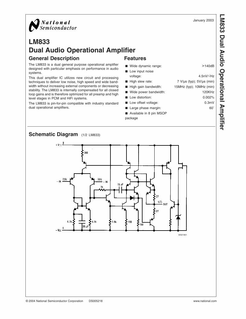
Connection Diagram
00521802
Order Number LM833M, LM833MX, LM833N, LM833MM or LM833MMXSee NS Package NumberM08A, N08E or MUA08A
LM83
3
www.national.com 2
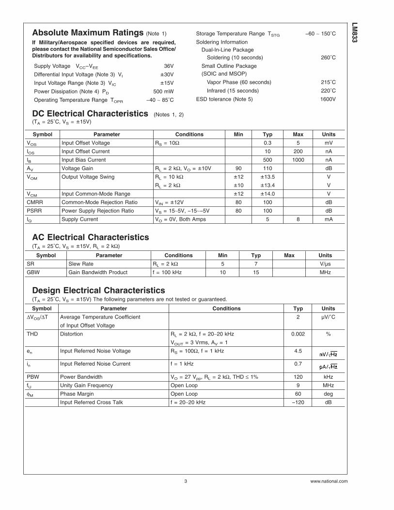
Absolute Maximum Ratings (Note 1)
If Military/Aerospace specified devices are required,please contact the National Semiconductor Sales Office/Distributors for availability and specifications.
Supply Voltage VCC–VEE 36V
Differential Input Voltage (Note 3) VI ±30V
Input Voltage Range (Note 3) VIC ±15V
Power Dissipation (Note 4) PD 500 mW
Operating Temperature Range TOPR −40 ∼ 85˚C
Storage Temperature Range TSTG −60 ∼ 150˚C
Soldering InformationDual-In-Line Package
Soldering (10 seconds) 260˚C
Small Outline Package(SOIC and MSOP)
Vapor Phase (60 seconds) 215˚C
Infrared (15 seconds) 220˚C
ESD tolerance (Note 5) 1600V
DC Electrical Characteristics (Notes 1, 2)(TA = 25˚C, VS = ±15V)
Symbol Parameter Conditions Min Typ Max Units
VOS Input Offset Voltage RS = 10Ω 0.3 5 mV
IOS Input Offset Current 10 200 nA
IB Input Bias Current 500 1000 nA
AV Voltage Gain RL = 2 kΩ, VO = ±10V 90 110 dB
VOM Output Voltage Swing RL = 10 kΩ ±12 ±13.5 V
RL = 2 kΩ ±10 ±13.4 V
VCM Input Common-Mode Range ±12 ±14.0 V
CMRR Common-Mode Rejection Ratio VIN = ±12V 80 100 dB
PSRR Power Supply Rejection Ratio VS = 15∼5V, −15∼−5V 80 100 dB
IQ Supply Current VO = 0V, Both Amps 5 8 mA
AC Electrical Characteristics(TA = 25˚C, VS = ±15V, RL = 2 kΩ)
Symbol Parameter Conditions Min Typ Max Units
SR Slew Rate RL = 2 kΩ 5 7 V/µs
GBW Gain Bandwidth Product f = 100 kHz 10 15 MHz
Design Electrical Characteristics(TA = 25˚C, VS = ±15V) The following parameters are not tested or guaranteed.
Symbol Parameter Conditions Typ Units
∆VOS/∆T Average Temperature Coefficient 2 µV/˚C
of Input Offset Voltage
THD Distortion RL = 2 kΩ, f = 20∼20 kHz 0.002 %
VOUT = 3 Vrms, AV = 1
en Input Referred Noise Voltage RS = 100Ω, f = 1 kHz 4.5
in Input Referred Noise Current f = 1 kHz 0.7
PBW Power Bandwidth VO = 27 Vpp, RL = 2 kΩ, THD ≤ 1% 120 kHz
fU Unity Gain Frequency Open Loop 9 MHz
φM Phase Margin Open Loop 60 deg
Input Referred Cross Talk f = 20∼20 kHz −120 dB
LM833
www.national.com3
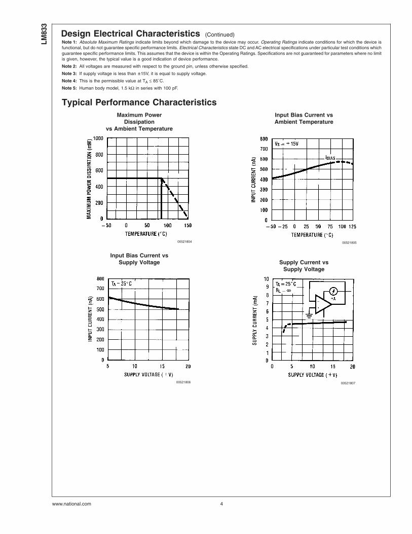
Design Electrical Characteristics (Continued)Note 1: Absolute Maximum Ratings indicate limits beyond which damage to the device may occur. Operating Ratings indicate conditions for which the device isfunctional, but do not guarantee specific performance limits. Electrical Characteristics state DC and AC electrical specifications under particular test conditions whichguarantee specific performance limits. This assumes that the device is within the Operating Ratings. Specifications are not guaranteed for parameters where no limitis given, however, the typical value is a good indication of device performance.
Note 2: All voltages are measured with respect to the ground pin, unless otherwise specified.
Note 3: If supply voltage is less than ±15V, it is equal to supply voltage.
Note 4: This is the permissible value at TA ≤ 85˚C.
Note 5: Human body model, 1.5 kΩ in series with 100 pF.
Typical Performance CharacteristicsMaximum Power
Dissipationvs Ambient Temperature
Input Bias Current vsAmbient Temperature
00521804 00521805
Input Bias Current vsSupply Voltage Supply Current vs
Supply Voltage
00521806 00521807
LM83
3
www.national.com 4
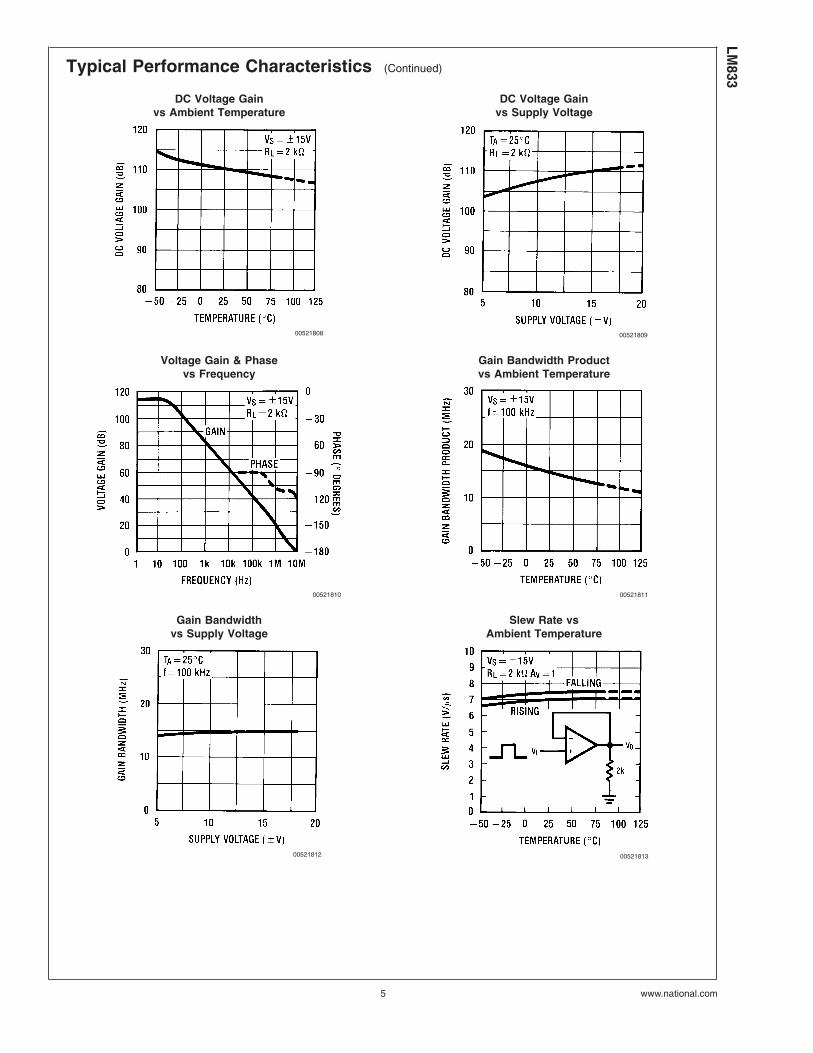
Typical Performance Characteristics (Continued)
DC Voltage Gainvs Ambient Temperature
DC Voltage Gainvs Supply Voltage
00521808 00521809
Voltage Gain & Phasevs Frequency
Gain Bandwidth Productvs Ambient Temperature
00521810 00521811
Gain Bandwidthvs Supply Voltage
Slew Rate vsAmbient Temperature
00521812 00521813
LM833
www.national.com5
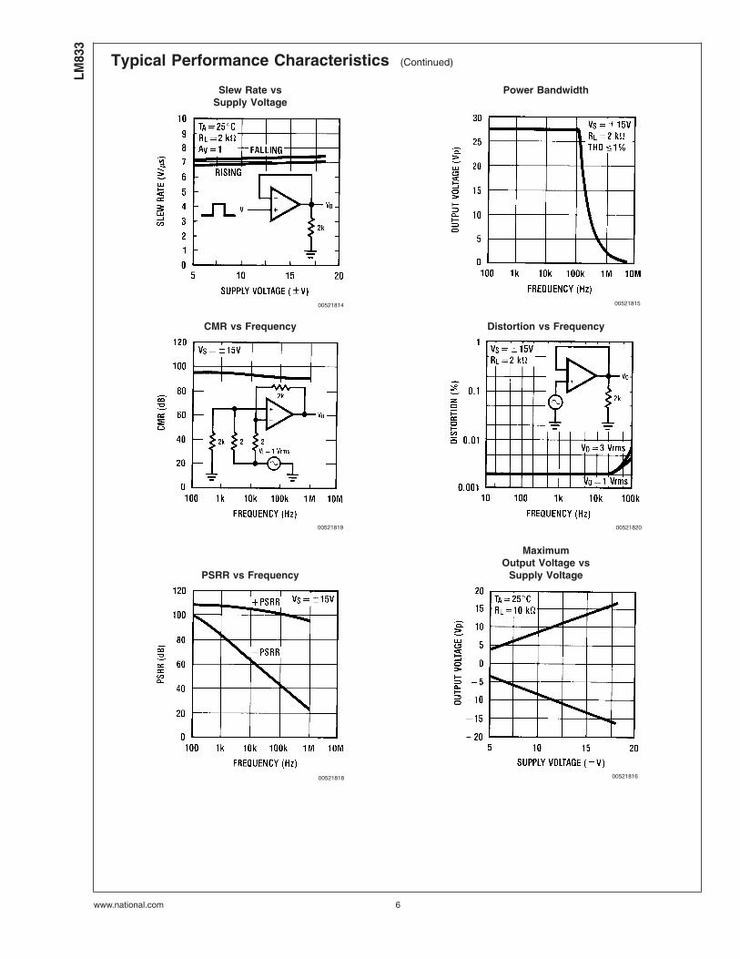
Typical Performance Characteristics (Continued)
Slew Rate vsSupply Voltage
Power Bandwidth
00521814 00521815
CMR vs Frequency Distortion vs Frequency
00521819 00521820
PSRR vs Frequency
MaximumOutput Voltage vs
Supply Voltage
00521818 00521816
LM83
3
www.national.com 6
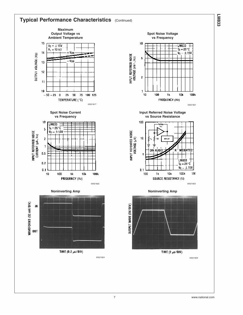
Typical Performance Characteristics (Continued)
MaximumOutput Voltage vs
Ambient TemperatureSpot Noise Voltage
vs Frequency
00521817 00521821
Spot Noise Currentvs Frequency
Input Referred Noise Voltagevs Source Resistance
00521822 00521823
Noninverting Amp Noninverting Amp
00521824 00521825
LM833
www.national.com7
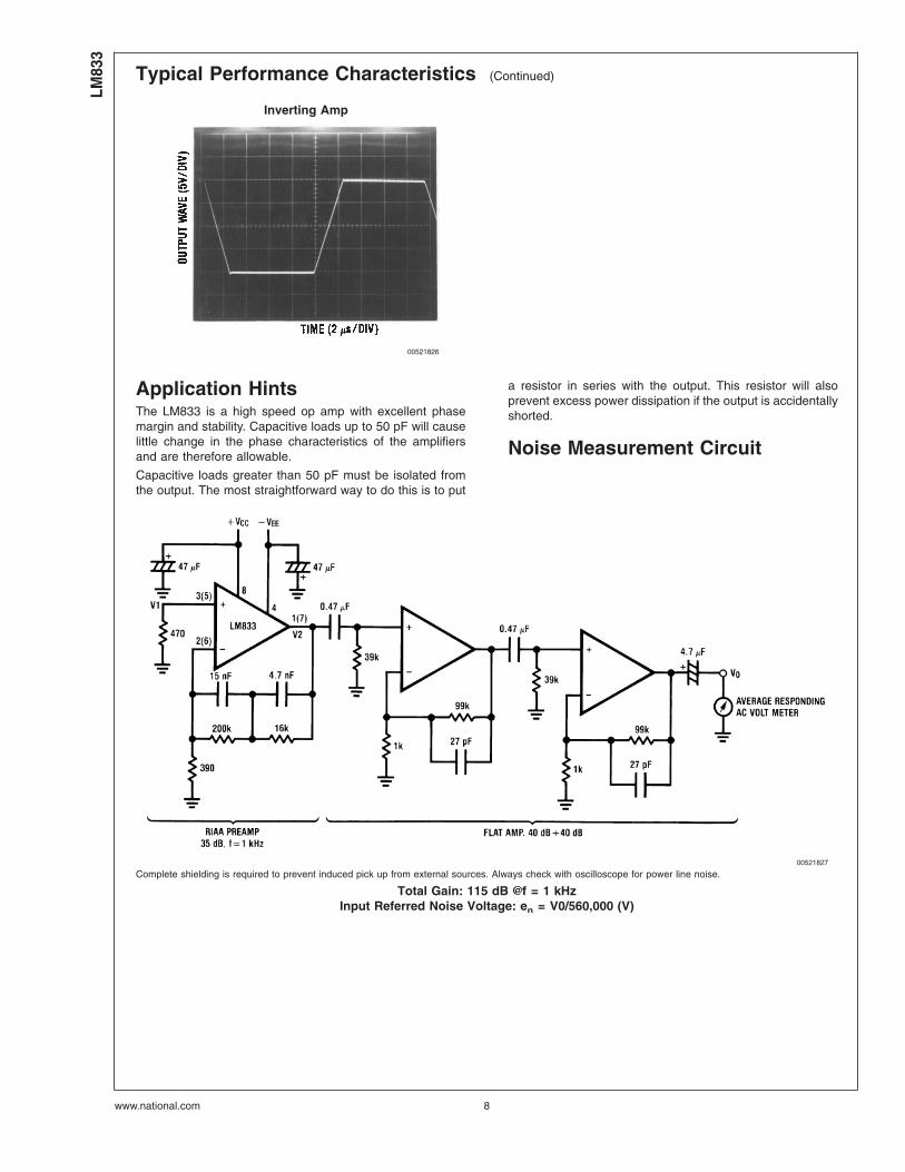
Typical Performance Characteristics (Continued)
Inverting Amp
00521826
Application HintsThe LM833 is a high speed op amp with excellent phasemargin and stability. Capacitive loads up to 50 pF will causelittle change in the phase characteristics of the amplifiersand are therefore allowable.
Capacitive loads greater than 50 pF must be isolated fromthe output. The most straightforward way to do this is to put
a resistor in series with the output. This resistor will alsoprevent excess power dissipation if the output is accidentallyshorted.
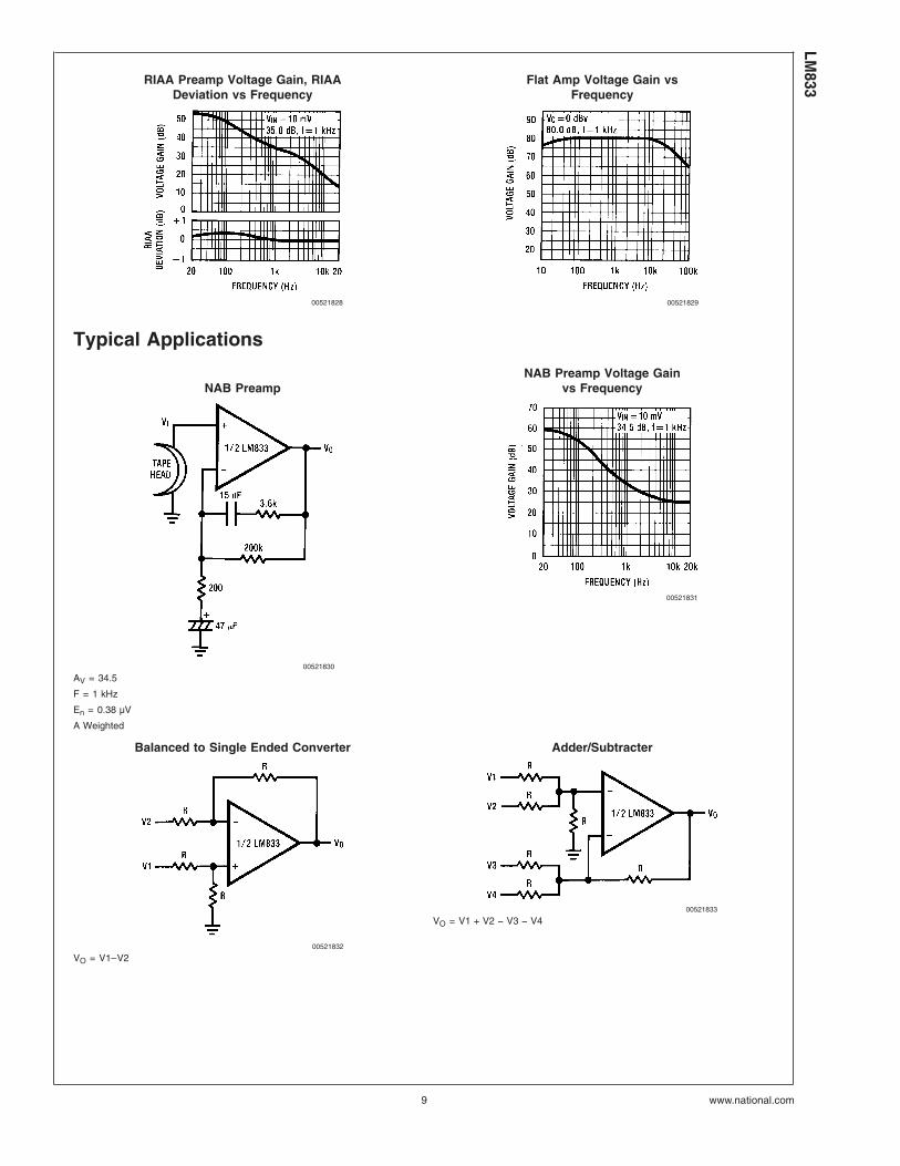
Noise Measurement Circuit
00521827
Complete shielding is required to prevent induced pick up from external sources. Always check with oscilloscope for power line noise.
Total Gain: 115 dB @f = 1 kHzInput Referred Noise Voltage: en = V0/560,000 (V)
LM83
3
www.national.com 8
RIAA Preamp Voltage Gain, RIAADeviation vs Frequency
Flat Amp Voltage Gain vsFrequency
00521828 00521829
Typical Applications
NAB PreampNAB Preamp Voltage Gain
vs Frequency
00521830
AV = 34.5
F = 1 kHz
En = 0.38 µV
A Weighted
00521831
Balanced to Single Ended Converter Adder/Subtracter
00521832
VO = V1–V2
00521833
VO = V1 + V2 − V3 − V4
LM833
www.national.com9
Typical Applications (Continued)
Sine Wave Oscillator
00521834
Second Order High Pass Filter(Butterworth)
Second Order Low Pass Filter(Butterworth)
00521835
Illustration is f0 = 1 kHz
00521836
Illustration is f0 = 1 kHz
LM83
3
www.national.com 10
Typical Applications (Continued)
State Variable Filter
00521837
Illustration is f0 = 1 kHz, Q = 10, ABP = 1
AC/DC Converter
00521838
2 Channel Panning Circuit (Pan Pot) Line Driver
00521839 00521840
LM833
www.national.com11
Typical Applications (Continued)
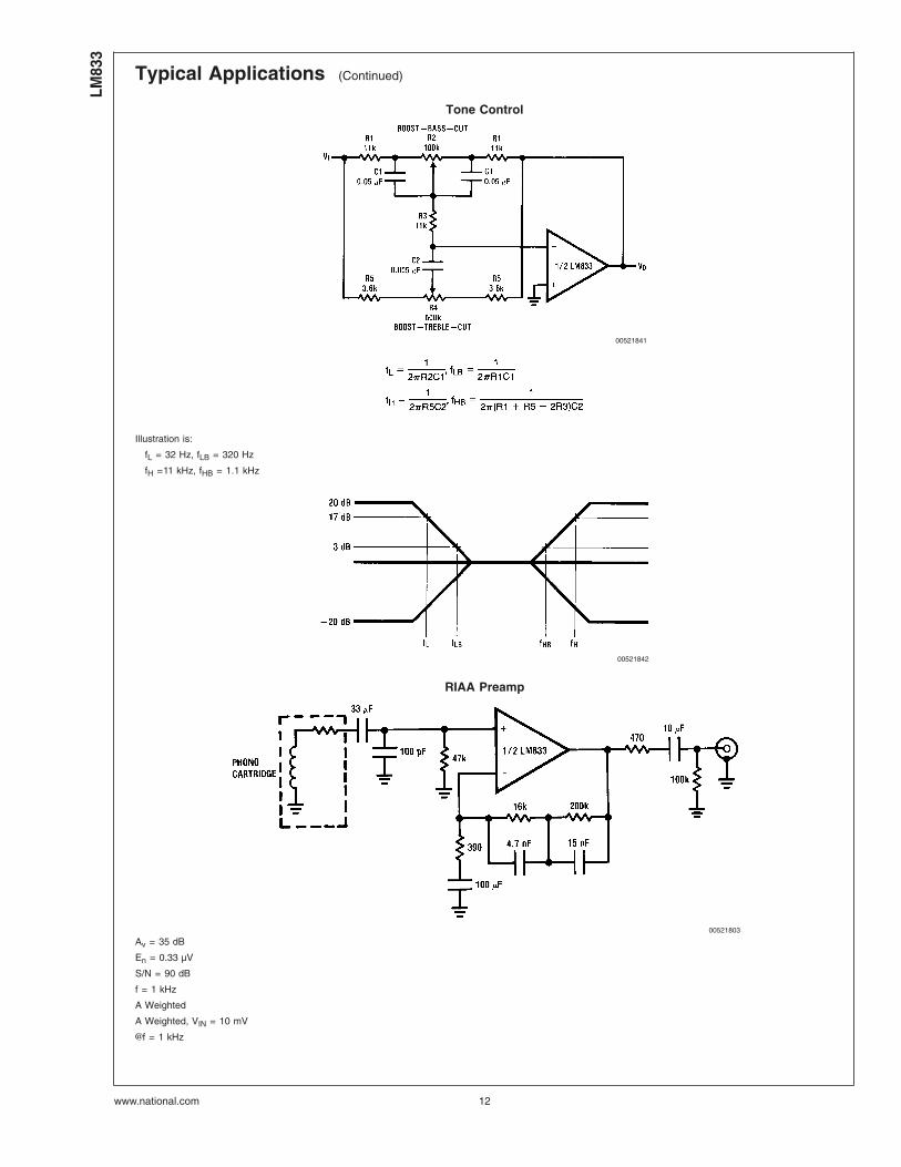
Tone Control
00521841
Illustration is:
fL = 32 Hz, fLB = 320 Hz
fH =11 kHz, fHB = 1.1 kHz
00521842
RIAA Preamp
00521803
Av = 35 dB
En = 0.33 µV
S/N = 90 dB
f = 1 kHz
A Weighted
A Weighted, VIN = 10 mV
@f = 1 kHz
LM83
3
www.national.com 12
Typical Applications (Continued)
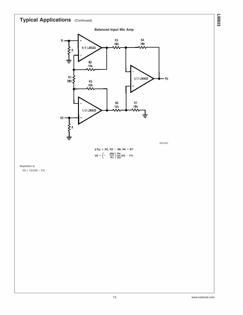
Balanced Input Mic Amp
00521843
Illustration is:
V0 = 101(V2 − V1)
LM833
www.national.com13
Typical Applications (Continued)
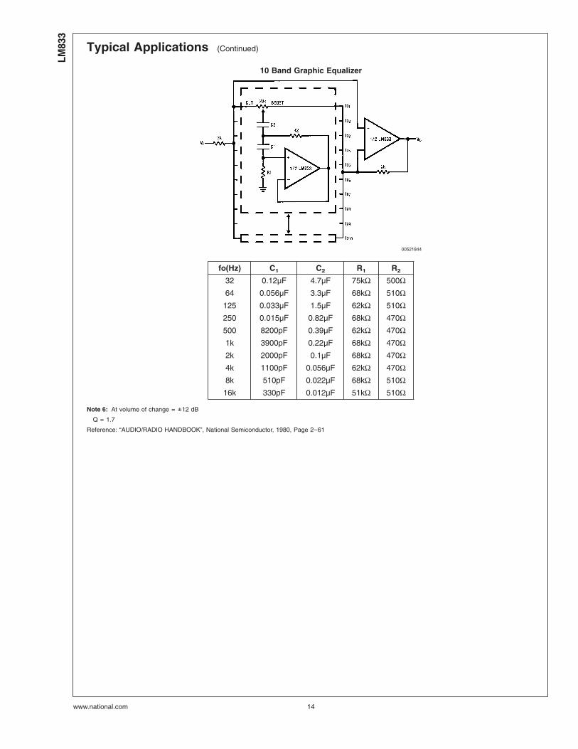
10 Band Graphic Equalizer
00521844
fo(Hz) C1 C2 R1 R2
32 0.12µF 4.7µF 75kΩ 500Ω64 0.056µF 3.3µF 68kΩ 510Ω
125 0.033µF 1.5µF 62kΩ 510Ω250 0.015µF 0.82µF 68kΩ 470Ω500 8200pF 0.39µF 62kΩ 470Ω1k 3900pF 0.22µF 68kΩ 470Ω2k 2000pF 0.1µF 68kΩ 470Ω4k 1100pF 0.056µF 62kΩ 470Ω8k 510pF 0.022µF 68kΩ 510Ω16k 330pF 0.012µF 51kΩ 510Ω
Note 6: At volume of change = ±12 dB
Q = 1.7
Reference: “AUDIO/RADIO HANDBOOK”, National Semiconductor, 1980, Page 2–61
LM83
3
www.national.com 14
Typical Applications (Continued)
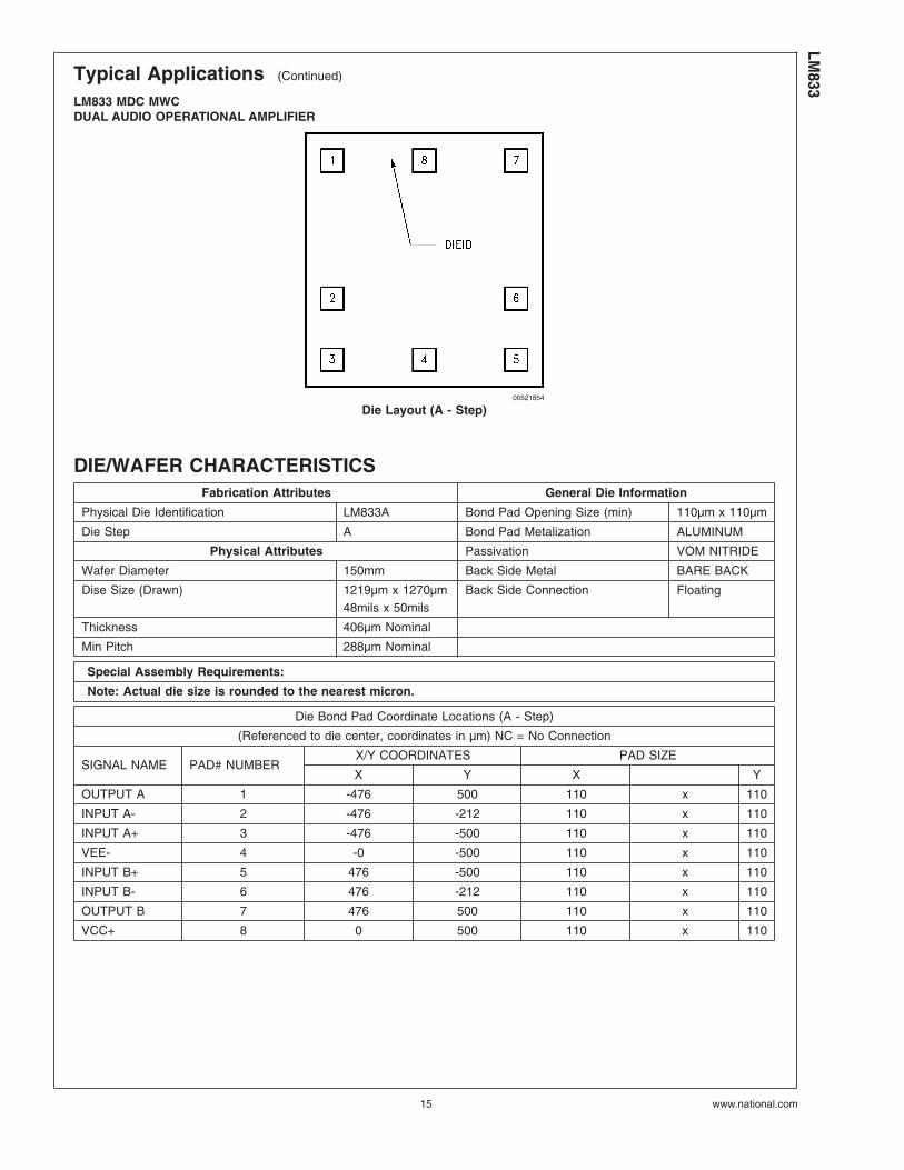
LM833 MDC MWCDUAL AUDIO OPERATIONAL AMPLIFIER
00521854
Die Layout (A - Step)
DIE/WAFER CHARACTERISTICSFabrication Attributes General Die Information
Physical Die Identification LM833A Bond Pad Opening Size (min) 110µm x 110µm
Die Step A Bond Pad Metalization ALUMINUM
Physical Attributes Passivation VOM NITRIDE
Wafer Diameter 150mm Back Side Metal BARE BACK
Dise Size (Drawn) 1219µm x 1270µm48mils x 50mils
Back Side Connection Floating
Thickness 406µm Nominal
Min Pitch 288µm Nominal
Special Assembly Requirements:
Note: Actual die size is rounded to the nearest micron.
Die Bond Pad Coordinate Locations (A - Step)
(Referenced to die center, coordinates in µm) NC = No Connection
SIGNAL NAME PAD# NUMBERX/Y COORDINATES PAD SIZE
X Y X Y
OUTPUT A 1 -476 500 110 x 110
INPUT A- 2 -476 -212 110 x 110
INPUT A+ 3 -476 -500 110 x 110
VEE- 4 -0 -500 110 x 110
INPUT B+ 5 476 -500 110 x 110
INPUT B- 6 476 -212 110 x 110
OUTPUT B 7 476 500 110 x 110
VCC+ 8 0 500 110 x 110
LM833
www.national.com15
Typical Applications (Continued)
IN U.S.A
Tel #: 1 877 Dial Die 1 877 342 5343
Fax: 1 207 541 6140
IN EUROPE
Tel: 49 (0) 8141 351492 / 1495
Fax: 49 (0) 8141 351470
IN ASIA PACIFIC
Tel: (852) 27371701
IN JAPAN
Tel: 81 043 299 2308
LM83
3
www.national.com 16
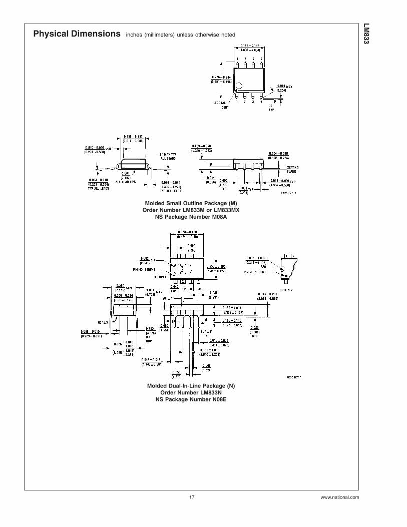
Physical Dimensions inches (millimeters) unless otherwise noted
Molded Small Outline Package (M)Order Number LM833M or LM833MX
NS Package Number M08A
Molded Dual-In-Line Package (N)Order Number LM833N
NS Package Number N08E
LM833
www.national.com17
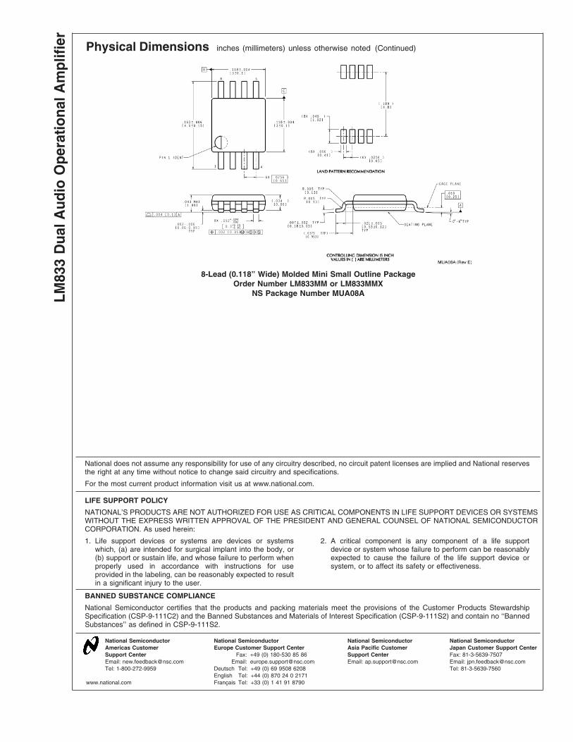
Physical Dimensions inches (millimeters) unless otherwise noted (Continued)
8-Lead (0.118” Wide) Molded Mini Small Outline PackageOrder Number LM833MM or LM833MMX
NS Package Number MUA08A
National does not assume any responsibility for use of any circuitry described, no circuit patent licenses are implied and National reservesthe right at any time without notice to change said circuitry and specifications.
For the most current product information visit us at www.national.com.
LIFE SUPPORT POLICY
NATIONAL’S PRODUCTS ARE NOT AUTHORIZED FOR USE AS CRITICAL COMPONENTS IN LIFE SUPPORT DEVICES OR SYSTEMSWITHOUT THE EXPRESS WRITTEN APPROVAL OF THE PRESIDENT AND GENERAL COUNSEL OF NATIONAL SEMICONDUCTORCORPORATION. As used herein:
1. Life support devices or systems are devices or systemswhich, (a) are intended for surgical implant into the body, or(b) support or sustain life, and whose failure to perform whenproperly used in accordance with instructions for useprovided in the labeling, can be reasonably expected to resultin a significant injury to the user.
2. A critical component is any component of a life supportdevice or system whose failure to perform can be reasonablyexpected to cause the failure of the life support device orsystem, or to affect its safety or effectiveness.
BANNED SUBSTANCE COMPLIANCE
National Semiconductor certifies that the products and packing materials meet the provisions of the Customer Products StewardshipSpecification (CSP-9-111C2) and the Banned Substances and Materials of Interest Specification (CSP-9-111S2) and contain no ‘‘BannedSubstances’’ as defined in CSP-9-111S2.
National SemiconductorAmericas CustomerSupport CenterEmail: [email protected]: 1-800-272-9959
National SemiconductorEurope Customer Support Center
Fax: +49 (0) 180-530 85 86Email: [email protected]
Deutsch Tel: +49 (0) 69 9508 6208English Tel: +44 (0) 870 24 0 2171Français Tel: +33 (0) 1 41 91 8790
National SemiconductorAsia Pacific CustomerSupport CenterEmail: [email protected]
National SemiconductorJapan Customer Support CenterFax: 81-3-5639-7507Email: [email protected]: 81-3-5639-7560
www.national.com
LM83
3D
ualA
udio
Ope
ratio
nalA
mpl
ifier