LM5113 - Datasheet - Texas Instruments · in a standard WSON-10 pin package and a 12-bump DSBGA...
27
LM5113 HB HOH HOL HS VDD HI LI LOH LOL VSS 0.1 F VIN 1 F EP Load Input Filter 1 Input Filter 2 Copyright © 2017, Texas Instruments Incorporated Product Folder Order Now Technical Documents Tools & Software Support & Community An IMPORTANT NOTICE at the end of this data sheet addresses availability, warranty, changes, use in safety-critical applications, intellectual property matters and other important disclaimers. PRODUCTION DATA. LM5113 SNVS725H – JUNE 2011 – REVISED JANUARY 2018 LM5113 80-V, 1.2-A, 5-A, Half Bridge GaN Driver (NRND) Not Recommended for New Designs 1 1 Features 1• Independent High-Side and Low-Side TTL Logic Inputs • 1.2 A / 5 A Peak Source / Sink Current • High-Side Floating Bias Voltage Rail Operates up to 100 VDC • Internal Bootstrap Supply Voltage Clamping • Split Outputs for Adjustable Turnon/Turnoff Strength • 0.6-Ω / 2.1-Ω Pulldown / Pullup Resistance • Fast Propagation Times (28 ns Typical) • Excellent Propagation Delay Matching (1.5 ns Typical) • Supply Rail Undervoltage Lockout • Low Power Consumption 2 Applications • Current Fed Push-Pull Converters • Half and Full-Bridge Converters • Synchronous Buck Converters • Two-Switch Forward Converters • Forward With Active Clamp Converters 3 Description The LM5113 device is designed to drive both the high-side and the low-side enhancement mode Gallium Nitride (GaN) FETs in a synchronous buck or a half bridge configuration. The floating high-side driver is capable of driving a high-side enhancement mode GaN FET operating up to 100 V. The high-side bias voltage is generated using a bootstrap technique and is internally clamped at 5.2 V, which prevents the gate voltage from exceeding the maximum gate- source voltage rating of enhancement mode GaN FETs. The inputs of the LM5113 are TTL logic compatible, and can withstand input voltages up to 14 V regardless of the VDD voltage. The LM5113 has split gate outputs, providing flexibility to adjust the turnon and turnoff strength independently. The LMG1205 is an enhancement over the LM5113. The LMG1205 takes the design of the LM5113 and includes start-up logic, level shifter, and power-off Vgs clamp enhancements to provide a more robust solution. In addition, the strong sink capability of the LM5113 maintains the gate in the low state, preventing unintended turnon during switching. The LM5113 can operate up to several MHz. The LM5113 is available in a standard WSON-10 pin package and a 12-bump DSBGA package. The WSON-10 pin package contains an exposed pad to aid power dissipation. The DSBGA package offers a compact footprint and minimized package inductance. Device Information (1) PART NUMBER PACKAGE BODY SIZE (NOM) LM5113 WSON (10) 4.00 mm × 4.00 mm DSBGA (12) 2.00 mm × 2.00 mm (1) For all available packages, see the orderable addendum at the end of the data sheet. Simplified Application Diagram
Transcript of LM5113 - Datasheet - Texas Instruments · in a standard WSON-10 pin package and a 12-bump DSBGA...

LM5113
HBHOH
HOL
HS
VDD
HI
LI LOH
LOL
VSS
0.1 FVIN
1 F
EP
LoadInput Filter 1
Input Filter 2
Copyright © 2017, Texas Instruments Incorporated
Product
Folder
Order
Now
Technical
Documents
Tools &
Software
Support &Community
An IMPORTANT NOTICE at the end of this data sheet addresses availability, warranty, changes, use in safety-critical applications,intellectual property matters and other important disclaimers. PRODUCTION DATA.
LM5113SNVS725H –JUNE 2011–REVISED JANUARY 2018
LM5113 80-V, 1.2-A, 5-A, Half Bridge GaN Driver (NRND)Not Recommended for New Designs
1
1 Features1• Independent High-Side and Low-Side
TTL Logic Inputs• 1.2 A / 5 A Peak Source / Sink Current• High-Side Floating Bias Voltage Rail
Operates up to 100 VDC• Internal Bootstrap Supply Voltage Clamping• Split Outputs for Adjustable
Turnon/Turnoff Strength• 0.6-Ω / 2.1-Ω Pulldown / Pullup Resistance• Fast Propagation Times (28 ns Typical)• Excellent Propagation Delay Matching
(1.5 ns Typical)• Supply Rail Undervoltage Lockout• Low Power Consumption
2 Applications• Current Fed Push-Pull Converters• Half and Full-Bridge Converters• Synchronous Buck Converters• Two-Switch Forward Converters• Forward With Active Clamp Converters
3 DescriptionThe LM5113 device is designed to drive both thehigh-side and the low-side enhancement modeGallium Nitride (GaN) FETs in a synchronous buck ora half bridge configuration. The floating high-sidedriver is capable of driving a high-side enhancementmode GaN FET operating up to 100 V. The high-sidebias voltage is generated using a bootstrap techniqueand is internally clamped at 5.2 V, which prevents thegate voltage from exceeding the maximum gate-source voltage rating of enhancement mode GaNFETs. The inputs of the LM5113 are TTL logiccompatible, and can withstand input voltages up to 14V regardless of the VDD voltage. The LM5113 hassplit gate outputs, providing flexibility to adjust theturnon and turnoff strength independently.
The LMG1205 is an enhancement over the LM5113.The LMG1205 takes the design of the LM5113 andincludes start-up logic, level shifter, and power-offVgs clamp enhancements to provide a more robustsolution.
In addition, the strong sink capability of the LM5113maintains the gate in the low state, preventingunintended turnon during switching. The LM5113 canoperate up to several MHz. The LM5113 is availablein a standard WSON-10 pin package and a 12-bumpDSBGA package. The WSON-10 pin packagecontains an exposed pad to aid power dissipation.The DSBGA package offers a compact footprint andminimized package inductance.
Device Information(1)
PART NUMBER PACKAGE BODY SIZE (NOM)
LM5113WSON (10) 4.00 mm × 4.00 mmDSBGA (12) 2.00 mm × 2.00 mm
(1) For all available packages, see the orderable addendum atthe end of the data sheet.
Simplified Application Diagram

Not Recommended for New Designs
2
LM5113SNVS725H –JUNE 2011–REVISED JANUARY 2018 www.ti.com
Product Folder Links: LM5113
Submit Documentation Feedback Copyright © 2011–2018, Texas Instruments Incorporated
Table of Contents1 Features .................................................................. 12 Applications ........................................................... 13 Description ............................................................. 14 Revision History..................................................... 25 Pin Configuration and Functions ......................... 36 Specifications......................................................... 4
6.1 Absolute Maximum Ratings ...................................... 46.2 ESD Ratings.............................................................. 46.3 Recommended Operating Conditions....................... 46.4 Thermal Information ................................................. 46.5 Electrical Characteristics .......................................... 56.6 Switching Characteristics .......................................... 66.7 Typical Characteristics .............................................. 7
7 Detailed Description ............................................ 107.1 Overview ................................................................. 107.2 Functional Block Diagram ....................................... 10
7.3 Feature Description................................................. 107.4 Device Functional Modes........................................ 12
8 Application and Implementation ........................ 138.1 Application Information............................................ 138.2 Typical Application ................................................. 13
9 Power Supply Recommendations ...................... 1710 Layout................................................................... 18
10.1 Layout Guidelines ................................................. 1810.2 Layout Examples................................................... 19
11 Device and Documentation Support ................. 2011.1 Documentation Support ........................................ 2011.2 Community Resources.......................................... 2011.3 Trademarks ........................................................... 2011.4 Electrostatic Discharge Caution............................ 2011.5 Glossary ................................................................ 20
12 Mechanical, Packaging, and OrderableInformation ........................................................... 20
4 Revision HistoryNOTE: Page numbers for previous revisions may differ from page numbers in the current version.
Changes from Revision G (January 2016) to Revision H Page
• Changed data sheet title from: LM5113 100 V 1.2-A / 5-A, Half-Bridge Gate Driver for Enhancement Mode GaNFETs to: LM5113 80-V, 1.2-A, 5-A, Half Bridge GaN Driver (NRND) .................................................................................... 1
• Added Not Recommended for New Designs statement to the data sheet............................................................................. 1• Added content to the Description section .............................................................................................................................. 1• Changed the first page key graphic ....................................................................................................................................... 1• Removed HB to VDD parameter from the Absolute Maximum Ratings table........................................................................ 4• Changed the HS to VSS maximum from: 100 V to: 93 V....................................................................................................... 4• Changed the HB to VSS maximum from: 107 V to: V(HS) + 7 V........................................................................................... 4• Changed the human-body model value from: ±2000 to: ±1000 ............................................................................................. 4• Changed HS maximum from: 100 V to: 90 V ........................................................................................................................ 4• Changed the Functional Block Diagram ............................................................................................................................... 10• Changed the last paragraph and add new images to the Input and Output section ........................................................... 10• Added content to the Start-up and UVLO section ............................................................................................................... 11
Changes from Revision F (April 2013) to Revision G Page
• Added ESD Ratings table, Feature Description section, Device Functional Modes, Application and Implementationsection, Power Supply Recommendations section, Layout section, Device and Documentation Support section, andMechanical, Packaging, and Orderable Information section .................................................................................................. 1
Changes from Revision E (April 2013) to Revision F Page
• Changed layout of National Data Sheet to TI format ............................................................................................................. 1

VDD LI
HI
VDD
HSHBHOHHOL
HS
LOH
LOL VSSA
B
C
D
1 2 3 4
Thermal Pad
VDD 1
HB
HOH
HOL
LOH10
LOL
VSS
LI
HS HI
2 9
3 8
4 7
5 6
Not Recommended for New Designs
3
LM5113www.ti.com SNVS725H –JUNE 2011–REVISED JANUARY 2018
Product Folder Links: LM5113
Submit Documentation FeedbackCopyright © 2011–2018, Texas Instruments Incorporated
5 Pin Configuration and Functions
DPR Package10-Pin WSON With Exposed Thermal Pad
Top ViewYFX Package
12-Pin DSBGATop View
(1) I = Input, O = Output, G = Ground, P = Power(2) A3 and C4, C1 and D4 are internally connected
Pin FunctionsPIN
TYPE (1) DESCRIPTIONNAME WSON DSBGA
VDD 1 A3, C4 (2) P 5-V Positive gate drive supply: locally decouple to VSS using low ESR/ESL capacitorlocated as close to the IC as possible.
HB 2 D3 PHigh-side gate driver bootstrap rail: connect the positive terminal of the bootstrap capacitorto HB and the negative terminal to HS. The bootstrap capacitor should be placed as closeto the IC as possible.
HOH 3 D2 O High-side gate driver turnon output: connect to the gate of high-side GaN FET with a short,low inductance path. A gate resistor can be used to adjust the turnon speed.
HOL 4 D1 O High-side gate driver turnoff output: connect to the gate of high-side GaN FET with a short,low inductance path. A gate resistor can be used to adjust the turnoff speed.
HS 5 C1, D4 (2) P High-side GaN FET source connection: connect to the bootstrap capacitor negativeterminal and the source of the high-side GaN FET.
HI 6 B4 I High-side driver control input. The LM5113 inputs have TTL type thresholds. Unusedinputs should be tied to ground and not left open.
LI 7 A4 I Low-side driver control input. The LM5113 inputs have TTL type thresholds. Unused inputsshould be tied to ground and not left open.
VSS 8 A2 G Ground return: all signals are referenced to this ground.
LOL 9 A1 O Low-side gate driver sink-current output: connect to the gate of the low-side GaN FET witha short, low inductance path. A gate resistor can be used to adjust the turnoff speed.
LOH 10 B1 O Low-side gate driver source-current output: connect to the gate of high-side GaN FET witha short, low inductance path. A gate resistor can be used to adjust the turnon speed.
ExposedPad EP — — Exposed pad: TI recommends that the exposed pad on the bottom of the package be
soldered to ground plane on the printed-circuit board to aid thermal dissipation.

Not Recommended for New Designs
4
LM5113SNVS725H –JUNE 2011–REVISED JANUARY 2018 www.ti.com
Product Folder Links: LM5113
Submit Documentation Feedback Copyright © 2011–2018, Texas Instruments Incorporated
(1) Stresses beyond those listed under Absolute Maximum Ratings may cause permanent damage to the device. These are stress ratingsonly, which do not imply functional operation of the device at these or any other conditions beyond those indicated under RecommendedOperating Conditions. Exposure to absolute-maximum-rated conditions for extended periods may affect device reliability.
6 Specifications
6.1 Absolute Maximum Ratingsover operating free-air temperature range (unless otherwise noted) (1)
MIN MAX UNITVDD to VSS –0.3 7 VHB to HS –0.3 7 VLI or HI input –0.3 15 VLOH, LOL output –0.3 VDD + 0.3 VHOH, HOL output VHS – 0.3 VHB +0.3 VHS to VSS –5 93 VHB to VSS 0 VHS + 7 VOperating junction temperature 150 °CStorage temperature, Tstg –55 150 °C
(1) JEDEC document JEP155 states that 500-V HBM allows safe manufacturing with a standard ESD control process.(2) JEDEC document JEP157 states that 250-V CDM allows safe manufacturing with a standard ESD control process.
6.2 ESD RatingsVALUE UNIT
V(ESD) Electrostatic dischargeHuman-body model (HBM), per ANSI/ESDA/JEDEC JS-001 (1) ±2000
VCharged-device model (CDM), per JEDEC specification JESD22-C101 (2) ±1000
6.3 Recommended Operating Conditionsover operating free-air temperature range (unless otherwise noted)
MIN NOM MAX UNITVDD 4.5 5.5 VLI or HI input 0 14 VHS –5 90 VHB VHS + 4 VHS + 5.5 VHS slew rate 50 V/nsOperating junction temperature –40 125 °C
(1) For more information about traditional and new thermal metrics, see the Semiconductor and IC Package Thermal Metrics applicationreport.
6.4 Thermal Information
THERMAL METRIC (1)LM5113
UNITDPR (WSON) YFX (DSBGA)10 PINS 12 PINS
RθJA Junction-to-ambient thermal resistance 37.5 76.8 °C/WRθJC(top) Junction-to-case (top) thermal resistance 35.8 0.6 °C/WRθJB Junction-to-board thermal resistance 14.7 12.0 °C/WψJT Junction-to-top characterization parameter 0.3 1.6 °C/WψJB Junction-to-board characterization parameter 14.9 12.0 °C/WRθJC(bot) Junction-to-case (bottom) thermal resistance 4.1 – °C/W

Not Recommended for New Designs
5
LM5113www.ti.com SNVS725H –JUNE 2011–REVISED JANUARY 2018
Product Folder Links: LM5113
Submit Documentation FeedbackCopyright © 2011–2018, Texas Instruments Incorporated
(1) Minimum and maximum limits are 100% production tested at 25°C. Limits over the operating temperature range are ensured throughcorrelation using Statistical Quality Control (SQC) methods. Limits are used to calculate Average Outgoing Quality Level (AOQL).
6.5 Electrical CharacteristicsSpecifications are TJ = 25°C. Unless otherwise specified: VDD = VHB = 5 V, VSS = VHS = 0 V.No load on LOL and HOL or HOH and HOL (1).
PARAMETER TEST CONDITIONS MIN TYP MAX UNITSUPPLY CURRENTS
IDD VDD quiescent current LI = HI = 0 VTJ = 25°C 0.07
mATJ = –40°C to 125°C 0.1
IDDO VDD operating current f = 500 kHzTJ = 25°C 2.0
mATJ = –40°C to 125°C 3.0
IHB Total HB quiescent current LI = HI = 0 VTJ = 25°C 0.08
mATJ = –40°C to 125°C 0.1
IHBO Total HB operating current f = 500 kHzTJ = 25°C 1.5
mATJ = –40°C to 125°C 2.5
IHBS HB to VSS quiescent current HS = HB = 100 VTJ = 25°C 0.1
µATJ = –40°C to 125°C 8
IHBSO HB to VSS operating current f = 500 kHzTJ = 25°C 0.4
mATJ = –40°C to 125°C 1.0
INPUT PINS
VIR Input voltage threshold Rising edgeTJ = 25°C 2.06
VTJ = –40°C to 125°C 1.89 2.18
VIF Input voltage threshold Falling edgeTJ = 25°C 1.66
VTJ = –40°C to 125°C 1.48 1.76
VIHYS Input voltage hysteresis 400 mV
RI Input pulldown resistanceTJ = 25°C 200
kΩTJ = –40°C to 125°C 100 300
UNDERVOLTAGE PROTECTION
VDDR VDD rising thresholdTJ = 25°C 3.8
VTJ = –40°C to 125°C 3.2 4.5
VDDH VDD threshold hysteresis 0.2 V
VHBR HB rising thresholdTJ = 25°C 3.2
VTJ = –40°C to 125°C 2.5 3.9
VHBH HB threshold hysteresis 0.2 VBOOTSTRAP DIODE
VDL Low-current forward voltage IVDD-HB = 100 µATJ = 25°C 0.45
VTJ = –40°C to 125°C 0.65
VDH High-current forward voltage IVDD-HB = 100 mATJ = 25°C 0.90
VTJ = –40°C to 125°C 1.00
RD Dynamic resistance IVDD-HB = 100 mATJ = 25°C 1.85
ΩTJ = –40°C to 125°C 3.60
HB-HS clamp Regulation voltageTJ = 25°C 5.2
VTJ = –40°C to 125°C 4.7 5.45

Not Recommended for New Designs
6
LM5113SNVS725H –JUNE 2011–REVISED JANUARY 2018 www.ti.com
Product Folder Links: LM5113
Submit Documentation Feedback Copyright © 2011–2018, Texas Instruments Incorporated
Electrical Characteristics (continued)Specifications are TJ = 25°C. Unless otherwise specified: VDD = VHB = 5 V, VSS = VHS = 0 V.No load on LOL and HOL or HOH and HOL(1).
PARAMETER TEST CONDITIONS MIN TYP MAX UNITLOW- AND HIGH-SIDE GATE DRIVER
VOL Low-level output voltage IHOL = ILOL = 100 mATJ = 25°C 0.06
VTJ = –40°C to 125°C 0.10
VOH
High-level output voltageVOH = VDD – LOHor VOH = HB – HOH
IHOH = ILOH = 100 mATJ = 25°C 0.21
VTJ = –40°C to 125°C 0.31
IOHL Peak source current HOH, LOH = 0 V 1.2 AIOLL Peak sink current HOL, LOL = 5 V 5 AIOHLK High-level output leakage current HOH, LOH = 0 V TJ = –40°C to 125°C 1.5 µAIOLLK Low-level output leakage current HOL, LOL = 5 V TJ = –40°C to 125°C 1.5 µA
6.6 Switching Characteristicsover operating free-air temperature range (unless otherwise noted)
PARAMETER TEST CONDITIONS MIN TYP MAX UNIT
tLPHL LO turnoff propagation delay LI falling to LOL fallingTJ = 25°C 26.5
nsTJ = –40°C to 125°C 45.0
tLPLH LO turnon propagation delay LI rising to LOH risingTJ = 25°C 28.0
nsTJ = –40°C to 125°C 45.0
tHPHL HO turnoff propagation delay HI falling to HOL fallingTJ = 25°C 26.5
nsTJ = –40°C to 125°C 45.0
tHPLH HO turnon propagation delay HI rising to HOH risingTJ = 25°C 28.0
nsTJ = –40°C to 125°C 45.0
tMONDelay matchingLO on & HO off
TJ = 25°C 1.5ns
TJ = –40°C to 125°C 8.0
tMOFFDelay matchingLO off & HO on
TJ = 25°C 1.5ns
TJ = –40°C to 125°C 8.0tHRC HO rise time (0.5 V – 4.5 V) CL = 1000 pF 7.0 nstLRC LO rise time (0.5 V – 4.5 V) CL = 1000 pF 7.0 nstHFC HO fall time (0.5 V – 4.5 V) CL = 1000 pF 1.5 nstLFC LO fall time (0.5 V – 4.5 V) CL = 1000 pF 1.5 ns
tPWMinimum input pulse widththat changes the output 10 ns
tBSBootstrap diodereverse recovery time IF = 100 mA, IR = 100 mA 40 ns

LI
HI
tHPLHtLPLH
tHPHLtLPHL
LO
HO
LI
HI
tMOFFtMON
LO
HO
Not Recommended for New Designs
7
LM5113www.ti.com SNVS725H –JUNE 2011–REVISED JANUARY 2018
Product Folder Links: LM5113
Submit Documentation FeedbackCopyright © 2011–2018, Texas Instruments Incorporated
Figure 1. Timing Diagram
6.7 Typical Characteristics
Figure 2. Peak Source Current vs Output Voltage Figure 3. Peak Sink Current vs Output Voltage
Figure 4. IDDO vs Frequency Figure 5. IHBO vs Frequency

Not Recommended for New Designs
8
LM5113SNVS725H –JUNE 2011–REVISED JANUARY 2018 www.ti.com
Product Folder Links: LM5113
Submit Documentation Feedback Copyright © 2011–2018, Texas Instruments Incorporated
Typical Characteristics (continued)
Figure 6. IDD vs Temperature Figure 7. IHB vs Temperature
Figure 8. UVLO Rising Thresholds vs Temperature Figure 9. UVLO Falling Thresholds vs Temperature
Figure 10. Input Thresholds vs Temperature Figure 11. Input Threshold Hysteresis vs Temperature

Not Recommended for New Designs
9
LM5113www.ti.com SNVS725H –JUNE 2011–REVISED JANUARY 2018
Product Folder Links: LM5113
Submit Documentation FeedbackCopyright © 2011–2018, Texas Instruments Incorporated
Typical Characteristics (continued)
Figure 12. Bootstrap Diode Forward Voltage Figure 13. Propagation Delay vs Temperature
Note: Unless otherwise specified,VDD = VHB = 5 V, VSS = VHS = 0 V.
Figure 14. LO & HO Gate Drive – High/Low LevelOutput Voltage vs Temperature
Note: Unless otherwise specified,VDD = VHB = 5 V, VSS = VHS = 0 V.
Figure 15. HB Regulation Voltage vs Temperature

LOH
UVLO
HOHLEVELSHIFT
HB
HS
VDD
VSS
HI
LI
HOL
LOL
UVLO & CLAMP
Copyright © 2017, Texas Instruments Incorporated
EXT HI
EXT LI
Not Recommended for New Designs
10
LM5113SNVS725H –JUNE 2011–REVISED JANUARY 2018 www.ti.com
Product Folder Links: LM5113
Submit Documentation Feedback Copyright © 2011–2018, Texas Instruments Incorporated
7 Detailed Description
7.1 OverviewThe LM5113 is a high frequency high- and low- side gate driver for enhancement mode Gallium Nitride (GaN)FETs in a synchronous buck or a half bridge configuration. The floating high-side driver is capable of driving ahigh-side enhancement mode GaN FET operating up to 100 V. The high-side bias voltage is generated using abootstrap technique and is internally clamped at 5.2 V, which prevents the gate voltage from exceeding themaximum gate-source voltage rating of enhancement mode GaN FETs. The LM5113 has split gate outputs withstrong sink capability, providing flexibility to adjust the turnon and turnoff strength independently.
The LM5113 can operate up to several MHz, and available in a standard WSON-10 pin package and a 12-bumpDSBGA package. The WSON-10 pin package contains an exposed pad to aid power dissipation. The DSBGApackage offers a compact footprint and minimized package inductance.
7.2 Functional Block Diagram
7.3 Feature Description
7.3.1 Input and OutputThe inputs are independently controlled with TTL input thresholds, and can withstand voltages up to 14 Vregardless of the VDD voltage, which means it could be directly connected to the outputs of PWM controllerswith up to 14-V power supply, saving a buffer stage between output of higher-voltage powered controller, forexample LM5025 with 10 V, and input of the LM5113.
The output pulldown and pullup resistance of LM5113 is optimized for enhancement mode GaN FETs to achievehigh frequency and efficient operation. The 0.6-Ω pulldown resistance provides a robust low impedance turnoffpath necessary to eliminate undesired turnon induced by high dv/dt or high di/dt. The 2.1-Ω pullup resistancehelps reduce the ringing and over-shoot of the switch node voltage. The split outputs of the LM5113 offerflexibility to adjust the turnon and turnoff speed by independently adding additional impedance in either theturnon path, the turnoff path, or both.
100 k
50 pF
SN74LVC2G32YZP
HI
EXT HI
Copyright © 2017, Texas Instruments Incorporated
HI1 k
22 pF
EXT HI
Not Recommended for New Designs
11
LM5113www.ti.com SNVS725H –JUNE 2011–REVISED JANUARY 2018
Product Folder Links: LM5113
Submit Documentation FeedbackCopyright © 2011–2018, Texas Instruments Incorporated
Feature Description (continued)It is very important that the input signal of the two channels HI and LI, which has logic compatible threshold andhysteresis, must be tied to either VDD or VSS if they are not used. This inputs must not be left floating.
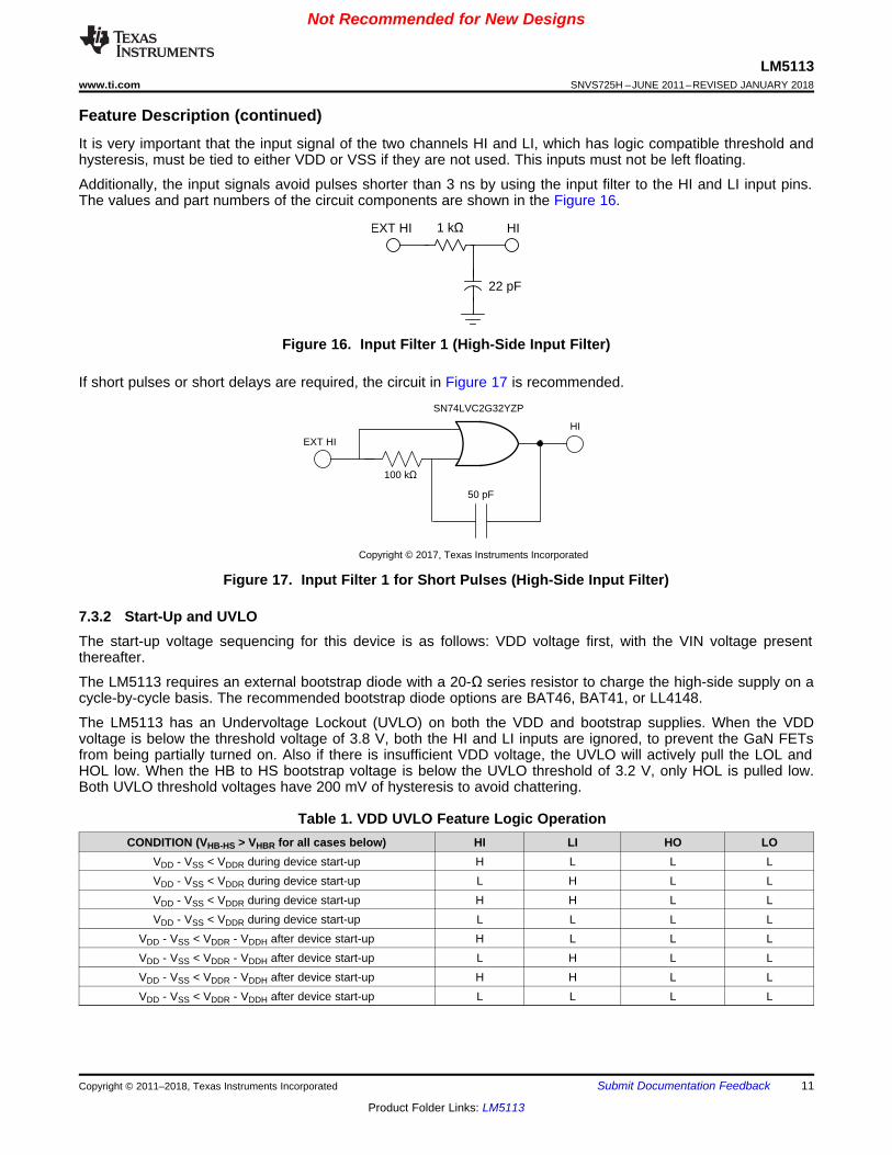
Additionally, the input signals avoid pulses shorter than 3 ns by using the input filter to the HI and LI input pins.The values and part numbers of the circuit components are shown in the Figure 16.
Figure 16. Input Filter 1 (High-Side Input Filter)
If short pulses or short delays are required, the circuit in Figure 17 is recommended.
Figure 17. Input Filter 1 for Short Pulses (High-Side Input Filter)
7.3.2 Start-Up and UVLOThe start-up voltage sequencing for this device is as follows: VDD voltage first, with the VIN voltage presentthereafter.
The LM5113 requires an external bootstrap diode with a 20-Ω series resistor to charge the high-side supply on acycle-by-cycle basis. The recommended bootstrap diode options are BAT46, BAT41, or LL4148.
The LM5113 has an Undervoltage Lockout (UVLO) on both the VDD and bootstrap supplies. When the VDDvoltage is below the threshold voltage of 3.8 V, both the HI and LI inputs are ignored, to prevent the GaN FETsfrom being partially turned on. Also if there is insufficient VDD voltage, the UVLO will actively pull the LOL andHOL low. When the HB to HS bootstrap voltage is below the UVLO threshold of 3.2 V, only HOL is pulled low.Both UVLO threshold voltages have 200 mV of hysteresis to avoid chattering.
Table 1. VDD UVLO Feature Logic OperationCONDITION (VHB-HS > VHBR for all cases below) HI LI HO LO
VDD - VSS < VDDR during device start-up H L L LVDD - VSS < VDDR during device start-up L H L LVDD - VSS < VDDR during device start-up H H L LVDD - VSS < VDDR during device start-up L L L L
VDD - VSS < VDDR - VDDH after device start-up H L L LVDD - VSS < VDDR - VDDH after device start-up L H L LVDD - VSS < VDDR - VDDH after device start-up H H L LVDD - VSS < VDDR - VDDH after device start-up L L L L

Not Recommended for New Designs
12
LM5113SNVS725H –JUNE 2011–REVISED JANUARY 2018 www.ti.com
Product Folder Links: LM5113
Submit Documentation Feedback Copyright © 2011–2018, Texas Instruments Incorporated
Table 2. VHB-HS UVLO Feature Logic OperationCONDITION (VDD > VDDR for all cases below) HI LI HO LO
VHB-HS < VHBR during device start-up H L L LVHB-HS < VHBR during device start-up L H L HVHB-HS < VHBR during device start-up H H L HVHB-HS < VHBR during device start-up L L L L
VHB-HS < VHBR - VHBH after device start-up H L L LVHB-HS < VHBR - VHBH after device start-up L H L HVHB-HS < VHBR - VHBH after device start-up H H L HVHB-HS < VHBR - VHBH after device start-up L L L L
7.3.3 HS Negative Voltage and Bootstrap Supply Voltage ClampingDue to the intrinsic feature of enhancement mode GaN FETs, the source-to-drain voltage of the bottom switch, isusually higher than a diode forward voltage drop when the gate is pulled low. This will cause negative voltage onHS pin. Moreover, this negative voltage transient will be even worse, considering layout and device drain/sourceparasitic inductances. With high side driver using the floating bootstrap configuration, Negative HS voltage canlead to an excessive bootstrap voltage which can damage the high-side GaN FET. The LM5113 solves thisproblem with an internal clamping circuit that prevents the bootstrap voltage from exceeding 5.2 V typical.
7.3.4 Level ShiftThe level shift circuit is the interface from the high-side input to the high-side driver stage which is referenced tothe switch node (HS). The level shift allows control of the HO output which is referenced to the HS pin andprovides excellent delay matching with the low-side driver. Typical delay matching between LO and HO is around1.5 ns.
7.4 Device Functional ModesTable 3 shows the device truth table.
Table 3. Truth TableHI LI HOH HOL LOH LOLL L Open L Open LL H Open L H OpenH L H Open Open LH H H Open H Open

Not Recommended for New Designs
13
LM5113www.ti.com SNVS725H –JUNE 2011–REVISED JANUARY 2018
Product Folder Links: LM5113
Submit Documentation FeedbackCopyright © 2011–2018, Texas Instruments Incorporated
8 Application and Implementation
NOTEInformation in the following applications sections is not part of the TI componentspecification, and TI does not warrant its accuracy or completeness. TI’s customers areresponsible for determining suitability of components for their purposes. Customers shouldvalidate and test their design implementation to confirm system functionality.
8.1 Application InformationTo operate GaN transistors at very high switching frequencies and to reduce associated switching losses, apowerful gate driver is employed between the PWM output of controller and the gates of the GaN transistor.Also, gate drivers are indispensable when it is impossible for the PWM controller to directly drive the gates of theswitching devices. With the advent of digital power, this situation is often encountered because the PWM signalfrom the digital controller is often a 3.3-V logic signal which cannot effectively turn on a power switch. Level shiftcircuit is required to boost the 3.3-V signal to the gate-drive voltage (such as 12 V) in order to fully turn on thepower device and minimize conduction losses. Traditional buffer drive circuits based on NPN/PNP bipolartransistors in totem-pole arrangement prove inadequate with digital power because they lack level-shiftingcapability. Gate drivers effectively combine both the level-shifting and buffer-drive functions. Gate drivers alsofind other needs such as minimizing the effect of high-frequency switching noise (by placing the high-currentdriver IC physically close to the power switch), driving gate-drive transformers and controlling floating power-device gates, reducing power dissipation and thermal stress in controllers by moving gate charge power lossesfrom the controller into the driver.
The LM5113 is a MHz high- and low-side gate driver for enhancement mode Gallium Nitride (GaN) FETs in asynchronous buck or a half bridge configuration. The floating high-side driver is capable of driving a high-sideenhancement mode GaN FET operating up to 100 V. The high-side bias voltage is generated using a bootstraptechnique and is internally clamped at 5.2 V, which prevents the gate voltage from exceeding the maximum gate-source voltage rating of enhancement mode GaN FETs. The LM5113 has split gate outputs with strong sinkcapability, providing flexibility to adjust the turnon and turnoff strength independently.
8.2 Typical ApplicationThe circuit in Figure 18 shows a synchronous buck converter to evaluate LM5113. Detailed synchronous buckconverter specifications are listed in Design Requirements. The active clamping voltage mode controller LM5025is used for close-loop control and generates the PWM signals of the buck switch and the synchronous switch.For more information, refer to the Related Documentation section.

2.2
F2.
2
F2.
2
F2.
2
F2.
2
F2.
2
FV
IN J3
C2
C3
C4
C5
C6
C7
VIN
J1
TP
4
+
+-
GN
D
GN
DG
ND
GN
D
GN
D
GN
D
OU
TIN O
N/O
FF
BY
PC
180.
1
FC
191
F
R7
33.2
kC
17N
U
R4
±1%
49
.9
U1
LP
2982
AIM
5-5.
05V
5 4
C20
100
pFC
212.
2
F
2
C24
1
F6.
3V
C25
0.1
F
GN
D
D3
NU
R11 0R
D4
GN
D
U3 HB
HS
VD
DH
OH
HI
HO
L
LOH
LOL
VS
S
LI
25 3 4 10 9
8761
EP
LM51
13
GN
D
NU
R14
0RC
27N
UC
28N
U
R15
4.02
k
¬¬¬¬
¬ ¬
¬ ¬ ¬
¬
R18
CO
MP
SY
NC
RT
TIM
ER
EF
VC
CA
GN
DP
GN
D
OU
TB
SS
RA
MP
OU
TA
UV
LOC
S2
CS
1V
IN
U4
16
1 2 12 15 14 6
3 4 8 9 13 5 11 107
LM50
25C
300.
01
FC
310.
1
F
R17
7.50
kC
321
F
GN
D
GN
D
0
D5
D6
MB
R13
0T1G
1N41
48W
-7-F
R19
21.0
k
GN
D
GN
D
R16
21.0
k
C29
1
F
GN
D
U2
LM82
61M
5C
261
F
C23
1500
pF
C22
330
pF
R8
16.9
k
2
41
5
3
R5
374
C15
1.5
nF
R6
21.0
k
R1
10.0
C1
330
FC
1222
F
C10
22
FC
111
FC
141
uF
C13
NU
SE
R13
60-2
72K
L2.
7
H
L1
1
23579
11
468
10
Q
2E
PC
2001
D2
MB
R13
0T1G
GN
D
GN
D
GN
D
J4
VO
UT
10V
J2V
OU
TT
P2
TP
5
1110
9 7 5 3
8 6 4 2 Q1
EP
C20
01
1
C9
0.01
uF
C8
0.1
uF
TP
3
TP
1E
X V
CC
GN
D
D1
MB
R13
0T1G
R2
100k
±1%
R3
150k
C16
220
pF
R13
6.98
k
R9
2RR
100R
¬
1 3
Not Recommended for New Designs
14
LM5113SNVS725H –JUNE 2011–REVISED JANUARY 2018 www.ti.com
Product Folder Links: LM5113
Submit Documentation Feedback Copyright © 2011–2018, Texas Instruments Incorporated
Typical Application (continued)
Input 15 V to 60 V, output 10 V, 800 kHz
Figure 18. Application Circuit

Not Recommended for New Designs
15
LM5113www.ti.com SNVS725H –JUNE 2011–REVISED JANUARY 2018
Product Folder Links: LM5113
Submit Documentation FeedbackCopyright © 2011–2018, Texas Instruments Incorporated
Typical Application (continued)8.2.1 Design RequirementsTable 4 lists the design requirements for the typical application.
Table 4. Design ParametersPARAMETER SPECIFICATION
Input operating range 15 – 60 VOutput voltage 10 V
Output current, 48-V input 10 AOutput current, 60-V input 7 A
Efficiency at 48 V, 10 A >90%Frequency 800 kHz
8.2.2 Detailed Design ProcedureThis procedure outlines the design considerations of LM5113 in a synchronous buck converter with enhancementmode Gallium Nitride (GaN) FET. Refer to Figure 18 for component names and network locations. For additionaldesign help, see Related Documentation.
8.2.2.1 VDD Bypass CapacitorThe VDD bypass capacitor provides the gate charge for the low-side and high-side transistors and to absorb thereverse recovery charge of the bootstrap diode. The required bypass capacitance can be calculated withEquation 1.
(1)
QgH and QgL are gate charge of the high-side and low-side transistors respectively. Qrr is the reverse recoverycharge of the bootstrap diode, which is typically around 4 nC. ΔV is the maximum allowable voltage drop acrossthe bypass capacitor. A 0.1-µF or larger value, good-quality, ceramic capacitor is recommended. The bypasscapacitor should be placed as close to the pins of the IC as possible to minimize the parasitic inductance.
8.2.2.2 Bootstrap CapacitorThe bootstrap capacitor provides the gate charge for the high-side switch, DC bias power for HB undervoltagelockout circuit, and the reverse recovery charge of the bootstrap diode. The required bypass capacitance can becalculated with Equation 2.
(2)
IHB is the quiescent current of the high-side driver. ton is the maximum on-time period of the high-side transistor.A good-quality, ceramic capacitor should be used for the bootstrap capacitor. TI recommends placing thebootstrap capacitor as close to the HB and HS pins as possible.
8.2.2.3 Power DissipationThe power consumption of the driver is an important measure that determines the maximum achievableoperating frequency of the driver. It should be kept below the maximum power dissipation limit of the package atthe operating temperature. The total power dissipation of the LM5113 is the sum of the gate driver losses and thebootstrap diode power loss.
The gate driver losses are incurred by charge and discharge of the capacitive load. It can be approximated as:
(3)
CLoadH and CLoadL are the high-side and the low-side capacitive loads, respectively. It can also be calculated withthe total input gate charge of the high-side and the low-side transistors as:
(4)

(TJ - TA)TJA
P =
Not Recommended for New Designs
16
LM5113SNVS725H –JUNE 2011–REVISED JANUARY 2018 www.ti.com
Product Folder Links: LM5113
Submit Documentation Feedback Copyright © 2011–2018, Texas Instruments Incorporated
There are some additional losses in the gate drivers due to the internal CMOS stages used to buffer the LO andHO outputs. The following plot shows the measured gate driver power dissipation versus frequency and loadcapacitance. At higher frequencies and load capacitance values, the power dissipation is dominated by thepower losses driving the output loads and agrees well with the above equations. This plot can be used toapproximate the power losses due to the gate drivers.
Gate Driver Power Dissipation (LO+HO), VDD = +5 V
Figure 19. Neglecting Bootstrap Diode Losses
The bootstrap diode power loss is the sum of the forward bias power loss that occurs while charging thebootstrap capacitor and the reverse bias power loss that occurs during reverse recovery. Because each of theseevents happens once per cycle, the diode power loss is proportional to the operating frequency. Largercapacitive loads require more energy to recharge the bootstrap capacitor resulting in more losses. Higher inputvoltages (VIN) to the half bridge also result in higher reverse recovery losses.
The following two plots illustrate the forward bias power loss and the reverse bias power loss of the bootstrapdiode respectively. The plots are generated based on calculations and lab measurements of the diode reversetime and current under several operating conditions. The plots can be used to predict the bootstrap diode powerloss under different operating conditions.
The Load of High-Side Driver is a GaN FET with Total Gate Chargeof 10 nC.
Figure 20. Forward Bias Power Loss ofBootstrap Diode VIN = 50 V
The Load of High-Side Driver is a GaN FET with Total Gate Chargeof 10 nC.
Figure 21. Reverse Recovery Power Loss ofBootstrap Diode VIN = 50 V
The sum of the driver loss and the bootstrap diode loss is the total power loss of the IC. For a given ambienttemperature, the maximum allowable power loss of the IC can be defined as Equation 5.
(5)

Not Recommended for New Designs
17
LM5113www.ti.com SNVS725H –JUNE 2011–REVISED JANUARY 2018
Product Folder Links: LM5113
Submit Documentation FeedbackCopyright © 2011–2018, Texas Instruments Incorporated
8.2.3 Application Curves
Conditions:Input Voltage = 48 V DC, Load Current = 5 ATraces:Top Trace: Gate of Low-Side eGaN FET, Volt/div = 2 VBottom Trace: LI of LM5113, Volt/div = 5 VBandwidth Limit = 600 MHzHorizontal Resolution = 0.2 µs/div
Figure 22. Low-Side Driver Input and Output
Conditions:Input Voltage = 48 V DC,Load Current = 10 ATraces:Trace: Switch-Node Voltage, Volts/div = 20 VBandwidth Limit = 600 MHzHorizontal Resolution = 50 ns/div
Figure 23. Switch-Node Voltage
9 Power Supply RecommendationsThe recommended bias supply voltage range for LM5113 is from 4.5 V to 5.5 V. The lower end of this range isgoverned by the internal undervoltage lockout (UVLO) protection feature of the VDD supply circuit. The upperend of this range is driven by the 7-V absolute maximum voltage rating of the VDD or the GaN transistor gatebreakdown voltage limit, whichever is lower. TI recommends keeping a proper margin to allow for transientvoltage spikes.
The UVLO protection feature also involves a hysteresis function. This means that once the device is operating innormal mode, if the VDD voltage drops, the device continues to operate in normal mode as far as the voltagedrop do not exceeds the hysteresis specification, VDDH. If the voltage drop is more than hysteresis specification,the device shuts down. Therefore, while operating at or near the 4.5-V range, the voltage ripple on the auxiliarypower supply output should be smaller than the hysteresis specification of LM5113 to avoid triggering deviceshutdown.
A local bypass capacitor should be placed between the VDD and VSS pins. And this capacitor should be locatedas close to the device as possible. A low-ESR, ceramic surface mount capacitor is recommended. TIrecommends using 2 capacitors across VDD and GND: a 100-nF ceramic surface-mount capacitor for highfrequency filtering placed very close to VDD and GND pin, and another surface-mount capacitor, 220-nF to 10-μF, for IC bias requirements.

Not Recommended for New Designs
18
LM5113SNVS725H –JUNE 2011–REVISED JANUARY 2018 www.ti.com
Product Folder Links: LM5113
Submit Documentation Feedback Copyright © 2011–2018, Texas Instruments Incorporated
10 Layout
10.1 Layout GuidelinesSmall gate capacitance and miller capacitance enable enhancement mode GaN FETs to operate with fastswitching speed. The induced high dv/dt and di/dt, coupled with a low gate threshold voltage and limitedheadroom of enhancement mode GaN FETs gate voltage, make the circuit layout crucial to the optimumperformance. Following are some hints.1. The first priority in designing the layout of the driver is to confine the high peak currents that charge and
discharge the GaN FETs gate into a minimal physical area. This will decrease the loop inductance andminimize noise issues on the gate terminal of the GaN FETs. The GaN FETs should be placed close to thedriver.
2. The second high current path includes the bootstrap capacitor, the local ground referenced VDD bypasscapacitor and low-side GaN FET. The bootstrap capacitor is recharged on a cycle-by-cycle basis through thebootstrap diode from the ground referenced VDD capacitor. The recharging occurs in a short time intervaland involves high peak current. Minimizing this loop length and area on the circuit board is important toensure reliable operation.
3. The parasitic inductance in series with the source of the high-side FET and the low-side FET can imposeexcessive negative voltage transients on the driver. TI recommends connecting the HS pin and VSS pin tothe respective source of the high-side and low-side transistors with a short and low-inductance path.
4. The parasitic source inductance, along with the gate capacitor and the driver pulldown path, can form a LCRresonant tank, resulting in gate voltage oscillations. An optional resistor or ferrite bead can be used to dampthe ringing.
5. Low ESR/ESL capacitors must be connected close to the IC, between VDD and VSS pins and between theHB and HS pins to support the high peak current being drawn from VDD during turnon of the FETs. Keepingbullet #1 (minimized GaN FETs gate driver loop) as the first priority, it is also desirable to place the VDDdecoupling capacitor and the HB to HS bootstrap capacitor on the same side of the printed-circuit board asthe driver. The inductance of vias can impose excessive ringing on the IC pins.
6. To prevent excessive ringing on the input power bus, good decoupling practices are required by placing low-ESR ceramic capacitors adjacent to the GaN FETs.
The following figures show recommended layout patterns for WSON-10 package and DSBGA package,respectively. Two cases are considered: (1) Without any gate resistors; (2) With an optional turnon gate resistor.It should be noted that 0402 DSBGA package is assumed for the passive components in the drawings. Forinformation on DSBGA package assembly, refer to Related Documentation.
spacer

A
B
C
D
1
To Hi-Side FETHO
To Low-Side FETLO
GNDBypass Capacitor
Bootstrap Capacitor
34
HS
2
VDDLI
HI
VDD
HS HB HOH HOL
LOH
LOLVSS
HS
A
B
C
D
12
To Hi-Side FETHO
To Low-Side FETLO
GND
Bypass Capacitor
Bootstrap Capacitor
HS
34
VDDLI
HI
VDD
HS HB HOH HOL
LOH
LOLVSS
HS
To Low-Side FETH
I
LI
VS
S
LOH
LOL
9 10
To Hi-Side FET
LO
GND
HS
6 7 8
125
VD
D
HB
Bypass Capacitor
4
HS
Bootstrap Capacitor
HO
HO
H
HO
L
3
To Low-Side FET
HI
LI
VS
S
LOH
LOL
9 10
To Hi-Side FET
LO
GND
HO
HS
6 7 8
12345
VD
D
HB
Bootstrap Capacitor
Bypass Capacitor
HS
Not Recommended for New Designs
19
LM5113www.ti.com SNVS725H –JUNE 2011–REVISED JANUARY 2018
Product Folder Links: LM5113
Submit Documentation FeedbackCopyright © 2011–2018, Texas Instruments Incorporated
10.2 Layout Examples
Figure 24. WSON-10 Without Gate Resistors Figure 25. WSON-10 With HOHand LOH Gate Resistors
Figure 26. DSBGA Without Gate Resistors Figure 27. DSBGA With HOHand LOH Gate Resistors

Not Recommended for New Designs
20
LM5113SNVS725H –JUNE 2011–REVISED JANUARY 2018 www.ti.com
Product Folder Links: LM5113
Submit Documentation Feedback Copyright © 2011–2018, Texas Instruments Incorporated
11 Device and Documentation Support
11.1 Documentation Support
11.1.1 Related DocumentationFor related documentation see the following:• AN-1112 DSBGA Wafer Level Chip Scale Package (SNVA009)• AN-2149 LM5113 Evaluation Board (SNVA484)
11.2 Community ResourcesThe following links connect to TI community resources. Linked contents are provided "AS IS" by the respectivecontributors. They do not constitute TI specifications and do not necessarily reflect TI's views; see TI's Terms ofUse.
TI E2E™ Online Community TI's Engineer-to-Engineer (E2E) Community. Created to foster collaborationamong engineers. At e2e.ti.com, you can ask questions, share knowledge, explore ideas and helpsolve problems with fellow engineers.
Design Support TI's Design Support Quickly find helpful E2E forums along with design support tools andcontact information for technical support.
11.3 TrademarksE2E is a trademark of Texas Instruments.All other trademarks are the property of their respective owners.
11.4 Electrostatic Discharge CautionThese devices have limited built-in ESD protection. The leads should be shorted together or the device placed in conductive foamduring storage or handling to prevent electrostatic damage to the MOS gates.
11.5 GlossarySLYZ022 — TI Glossary.
This glossary lists and explains terms, acronyms, and definitions.
12 Mechanical, Packaging, and Orderable InformationThe following pages include mechanical, packaging, and orderable information. This information is the mostcurrent data available for the designated devices. This data is subject to change without notice and revision ofthis document. For browser-based versions of this datasheet, refer to the left-hand navigation.

PACKAGE OPTION ADDENDUM
www.ti.com 15-Dec-2017
Addendum-Page 1
PACKAGING INFORMATION
Orderable Device Status(1)
Package Type PackageDrawing
Pins PackageQty
Eco Plan(2)
Lead/Ball Finish(6)
MSL Peak Temp(3)
Op Temp (°C) Device Marking(4/5)
Samples
LM5113SD/NOPB NRND WSON DPR 10 1000 Green (RoHS& no Sb/Br)
CU SN Level-1-260C-UNLIM -40 to 125 L5113
LM5113SDE/NOPB NRND WSON DPR 10 250 Green (RoHS& no Sb/Br)
CU SN Level-1-260C-UNLIM -40 to 125 L5113
LM5113SDX/NOPB NRND WSON DPR 10 4500 Green (RoHS& no Sb/Br)
CU SN Level-1-260C-UNLIM -40 to 125 L5113
LM5113TME/NOPB NRND DSBGA YFX 12 250 Green (RoHS& no Sb/Br)
SNAGCU Level-1-260C-UNLIM 5113
LM5113TMX/NOPB NRND DSBGA YFX 12 3000 Green (RoHS& no Sb/Br)
SNAGCU Level-1-260C-UNLIM 5113
(1) The marketing status values are defined as follows:ACTIVE: Product device recommended for new designs.LIFEBUY: TI has announced that the device will be discontinued, and a lifetime-buy period is in effect.NRND: Not recommended for new designs. Device is in production to support existing customers, but TI does not recommend using this part in a new design.PREVIEW: Device has been announced but is not in production. Samples may or may not be available.OBSOLETE: TI has discontinued the production of the device.
(2) RoHS: TI defines "RoHS" to mean semiconductor products that are compliant with the current EU RoHS requirements for all 10 RoHS substances, including the requirement that RoHS substancedo not exceed 0.1% by weight in homogeneous materials. Where designed to be soldered at high temperatures, "RoHS" products are suitable for use in specified lead-free processes. TI mayreference these types of products as "Pb-Free".RoHS Exempt: TI defines "RoHS Exempt" to mean products that contain lead but are compliant with EU RoHS pursuant to a specific EU RoHS exemption.Green: TI defines "Green" to mean the content of Chlorine (Cl) and Bromine (Br) based flame retardants meet JS709B low halogen requirements of <=1000ppm threshold. Antimony trioxide basedflame retardants must also meet the <=1000ppm threshold requirement.
(3) MSL, Peak Temp. - The Moisture Sensitivity Level rating according to the JEDEC industry standard classifications, and peak solder temperature.
(4) There may be additional marking, which relates to the logo, the lot trace code information, or the environmental category on the device.
(5) Multiple Device Markings will be inside parentheses. Only one Device Marking contained in parentheses and separated by a "~" will appear on a device. If a line is indented then it is a continuationof the previous line and the two combined represent the entire Device Marking for that device.
(6) Lead/Ball Finish - Orderable Devices may have multiple material finish options. Finish options are separated by a vertical ruled line. Lead/Ball Finish values may wrap to two lines if the finishvalue exceeds the maximum column width.

PACKAGE OPTION ADDENDUM
www.ti.com 15-Dec-2017
Addendum-Page 2
Important Information and Disclaimer:The information provided on this page represents TI's knowledge and belief as of the date that it is provided. TI bases its knowledge and belief on informationprovided by third parties, and makes no representation or warranty as to the accuracy of such information. Efforts are underway to better integrate information from third parties. TI has taken andcontinues to take reasonable steps to provide representative and accurate information but may not have conducted destructive testing or chemical analysis on incoming materials and chemicals.TI and TI suppliers consider certain information to be proprietary, and thus CAS numbers and other limited information may not be available for release.
In no event shall TI's liability arising out of such information exceed the total purchase price of the TI part(s) at issue in this document sold by TI to Customer on an annual basis.
OTHER QUALIFIED VERSIONS OF LM5113 :
• Automotive: LM5113-Q1
NOTE: Qualified Version Definitions:
• Automotive - Q100 devices qualified for high-reliability automotive applications targeting zero defects

TAPE AND REEL INFORMATION
*All dimensions are nominal
Device PackageType
PackageDrawing
Pins SPQ ReelDiameter
(mm)
ReelWidth
W1 (mm)
A0(mm)
B0(mm)
K0(mm)
P1(mm)
W(mm)
Pin1Quadrant
LM5113SD/NOPB WSON DPR 10 1000 178.0 12.4 4.3 4.3 1.3 8.0 12.0 Q1
LM5113SDE/NOPB WSON DPR 10 250 178.0 12.4 4.3 4.3 1.3 8.0 12.0 Q1
LM5113SDX/NOPB WSON DPR 10 4500 330.0 12.4 4.3 4.3 1.3 8.0 12.0 Q1
LM5113TME/NOPB DSBGA YFX 12 250 178.0 8.4 1.85 2.01 0.76 4.0 8.0 Q1
LM5113TMX/NOPB DSBGA YFX 12 3000 178.0 8.4 1.85 2.01 0.76 4.0 8.0 Q1
PACKAGE MATERIALS INFORMATION
www.ti.com 27-Oct-2017
Pack Materials-Page 1

*All dimensions are nominal
Device Package Type Package Drawing Pins SPQ Length (mm) Width (mm) Height (mm)
LM5113SD/NOPB WSON DPR 10 1000 210.0 185.0 35.0
LM5113SDE/NOPB WSON DPR 10 250 210.0 185.0 35.0
LM5113SDX/NOPB WSON DPR 10 4500 367.0 367.0 35.0
LM5113TME/NOPB DSBGA YFX 12 250 210.0 185.0 35.0
LM5113TMX/NOPB DSBGA YFX 12 3000 210.0 185.0 35.0
PACKAGE MATERIALS INFORMATION
www.ti.com 27-Oct-2017
Pack Materials-Page 2

MECHANICAL DATA
YFX0012xxx
www.ti.com
TMP12XXX (Rev A)
TOP SIDE OF PACKAGEBOTTOM SIDE OF PACKAGE
A. All linear dimensions are in millimeters. Dimensioning and tolerancing per ASME Y14.5M-1994.B. This drawing is subject to change without notice.
NOTES:
4215094/A 12/12
0.600±0.075
D
E
D: Max =
E: Max =
1.905 mm, Min =
1.756 mm, Min =
1.845 mm
1.695 mm

MECHANICAL DATA
DPR0010A
www.ti.com
SDC10A (Rev A)

IMPORTANT NOTICE
Texas Instruments Incorporated (TI) reserves the right to make corrections, enhancements, improvements and other changes to itssemiconductor products and services per JESD46, latest issue, and to discontinue any product or service per JESD48, latest issue. Buyersshould obtain the latest relevant information before placing orders and should verify that such information is current and complete.TI’s published terms of sale for semiconductor products (http://www.ti.com/sc/docs/stdterms.htm) apply to the sale of packaged integratedcircuit products that TI has qualified and released to market. Additional terms may apply to the use or sale of other types of TI products andservices.Reproduction of significant portions of TI information in TI data sheets is permissible only if reproduction is without alteration and isaccompanied by all associated warranties, conditions, limitations, and notices. TI is not responsible or liable for such reproduceddocumentation. Information of third parties may be subject to additional restrictions. Resale of TI products or services with statementsdifferent from or beyond the parameters stated by TI for that product or service voids all express and any implied warranties for theassociated TI product or service and is an unfair and deceptive business practice. TI is not responsible or liable for any such statements.Buyers and others who are developing systems that incorporate TI products (collectively, “Designers”) understand and agree that Designersremain responsible for using their independent analysis, evaluation and judgment in designing their applications and that Designers havefull and exclusive responsibility to assure the safety of Designers' applications and compliance of their applications (and of all TI productsused in or for Designers’ applications) with all applicable regulations, laws and other applicable requirements. Designer represents that, withrespect to their applications, Designer has all the necessary expertise to create and implement safeguards that (1) anticipate dangerousconsequences of failures, (2) monitor failures and their consequences, and (3) lessen the likelihood of failures that might cause harm andtake appropriate actions. Designer agrees that prior to using or distributing any applications that include TI products, Designer willthoroughly test such applications and the functionality of such TI products as used in such applications.TI’s provision of technical, application or other design advice, quality characterization, reliability data or other services or information,including, but not limited to, reference designs and materials relating to evaluation modules, (collectively, “TI Resources”) are intended toassist designers who are developing applications that incorporate TI products; by downloading, accessing or using TI Resources in anyway, Designer (individually or, if Designer is acting on behalf of a company, Designer’s company) agrees to use any particular TI Resourcesolely for this purpose and subject to the terms of this Notice.TI’s provision of TI Resources does not expand or otherwise alter TI’s applicable published warranties or warranty disclaimers for TIproducts, and no additional obligations or liabilities arise from TI providing such TI Resources. TI reserves the right to make corrections,enhancements, improvements and other changes to its TI Resources. TI has not conducted any testing other than that specificallydescribed in the published documentation for a particular TI Resource.Designer is authorized to use, copy and modify any individual TI Resource only in connection with the development of applications thatinclude the TI product(s) identified in such TI Resource. NO OTHER LICENSE, EXPRESS OR IMPLIED, BY ESTOPPEL OR OTHERWISETO ANY OTHER TI INTELLECTUAL PROPERTY RIGHT, AND NO LICENSE TO ANY TECHNOLOGY OR INTELLECTUAL PROPERTYRIGHT OF TI OR ANY THIRD PARTY IS GRANTED HEREIN, including but not limited to any patent right, copyright, mask work right, orother intellectual property right relating to any combination, machine, or process in which TI products or services are used. Informationregarding or referencing third-party products or services does not constitute a license to use such products or services, or a warranty orendorsement thereof. Use of TI Resources may require a license from a third party under the patents or other intellectual property of thethird party, or a license from TI under the patents or other intellectual property of TI.TI RESOURCES ARE PROVIDED “AS IS” AND WITH ALL FAULTS. TI DISCLAIMS ALL OTHER WARRANTIES ORREPRESENTATIONS, EXPRESS OR IMPLIED, REGARDING RESOURCES OR USE THEREOF, INCLUDING BUT NOT LIMITED TOACCURACY OR COMPLETENESS, TITLE, ANY EPIDEMIC FAILURE WARRANTY AND ANY IMPLIED WARRANTIES OFMERCHANTABILITY, FITNESS FOR A PARTICULAR PURPOSE, AND NON-INFRINGEMENT OF ANY THIRD PARTY INTELLECTUALPROPERTY RIGHTS. TI SHALL NOT BE LIABLE FOR AND SHALL NOT DEFEND OR INDEMNIFY DESIGNER AGAINST ANY CLAIM,INCLUDING BUT NOT LIMITED TO ANY INFRINGEMENT CLAIM THAT RELATES TO OR IS BASED ON ANY COMBINATION OFPRODUCTS EVEN IF DESCRIBED IN TI RESOURCES OR OTHERWISE. IN NO EVENT SHALL TI BE LIABLE FOR ANY ACTUAL,DIRECT, SPECIAL, COLLATERAL, INDIRECT, PUNITIVE, INCIDENTAL, CONSEQUENTIAL OR EXEMPLARY DAMAGES INCONNECTION WITH OR ARISING OUT OF TI RESOURCES OR USE THEREOF, AND REGARDLESS OF WHETHER TI HAS BEENADVISED OF THE POSSIBILITY OF SUCH DAMAGES.Unless TI has explicitly designated an individual product as meeting the requirements of a particular industry standard (e.g., ISO/TS 16949and ISO 26262), TI is not responsible for any failure to meet such industry standard requirements.Where TI specifically promotes products as facilitating functional safety or as compliant with industry functional safety standards, suchproducts are intended to help enable customers to design and create their own applications that meet applicable functional safety standardsand requirements. Using products in an application does not by itself establish any safety features in the application. Designers mustensure compliance with safety-related requirements and standards applicable to their applications. Designer may not use any TI products inlife-critical medical equipment unless authorized officers of the parties have executed a special contract specifically governing such use.Life-critical medical equipment is medical equipment where failure of such equipment would cause serious bodily injury or death (e.g., lifesupport, pacemakers, defibrillators, heart pumps, neurostimulators, and implantables). Such equipment includes, without limitation, allmedical devices identified by the U.S. Food and Drug Administration as Class III devices and equivalent classifications outside the U.S.TI may expressly designate certain products as completing a particular qualification (e.g., Q100, Military Grade, or Enhanced Product).Designers agree that it has the necessary expertise to select the product with the appropriate qualification designation for their applicationsand that proper product selection is at Designers’ own risk. Designers are solely responsible for compliance with all legal and regulatoryrequirements in connection with such selection.Designer will fully indemnify TI and its representatives against any damages, costs, losses, and/or liabilities arising out of Designer’s non-compliance with the terms and provisions of this Notice.
Mailing Address: Texas Instruments, Post Office Box 655303, Dallas, Texas 75265Copyright © 2018, Texas Instruments Incorporated