
LM5025 Active Clamp Voltage Mode PWM Controller (Rev. C) · LM5025 UVLO PGND AGND COMP OUT_A OUT_B...
32
LM5025 UVLO PGND AGND COMP OUT_A OUT_B VCC SS Rt SYNC REF TIME RAMP CS1 VIN CS2 VIN 35 - 78V VOUT 3.3V UP/DOWN SYNC ERROR AMP & ISOLATION Product Folder Sample & Buy Technical Documents Tools & Software Support & Community LM5025 SNVS265C – DECEMBER 2003 – REVISED JANUARY 2016 LM5025 Active Clamp Voltage Mode PWM Controller 1 Features 3 Description The LM5025 PWM controller contains all of the 1• Internal Start-Up Bias Regulator features necessary to implement power converters • 3-A Compound Main Gate Driver using the active clamp and reset technique. The • Programmable Line Undervoltage Lockout (UVLO) device can be configured to control either a With Adjustable Hysteresis P-channel clamp switch or an N-channel clamp switch. With the active clamp technique, higher • Voltage Mode Control With Feed-Forward efficiencies and greater power densities can be • Adjustable Dual-Mode Overcurrent Protection realized compared to conventional catch winding or • Programmable Overlap or Deadtime Between the RDC clamp and reset techniques. Main and Active Clamp Outputs Two control outputs are provided, the main power • Volt × Second Clamp switch control (OUT_A), and the active clamp switch • Programmable Soft-Start control (OUT_B). The active clamp output can be configured for either a specified overlap time • Leading Edge Blanking (for P-channel switch applications) or a specified • Single Resistor Programmable Oscillator deadtime (for N_channel applications). The two • Oscillator UP and DOWN Sync Capability internal compound gate drivers parallel both MOS • Precision 5-V Reference and bipolar devices, providing superior gate drive characteristics. This controller is designed for high- • Thermal Shutdown speed operation including an oscillator frequency range up to 1 MHz and total PWM and current sense 2 Applications propagation delays less than 100 ns. • Server Power Supplies The LM5025 includes a high-voltage start-up • 48-V Telecom Power Supplies regulator that operates over a wide input range of • 42-V Automotive Applications 13 V to 90 V. Additional features include: line undervoltage lockout (UVLO), soft-start, oscillator UP • High-Efficiency DC-to-DC Power Supplies and DOWN sync capability, precision reference and thermal shutdown. Device Information (1) PART NUMBER PACKAGE BODY SIZE (NOM) TSSOP (16) 5.00 mm × 4.40 mm LM5025 WSON (16) 5 00 mm × 5.00 mm (1) For all available packages, see the orderable addendum at the end of the data sheet. Simplified Schematic 1 An IMPORTANT NOTICE at the end of this data sheet addresses availability, warranty, changes, use in safety-critical applications, intellectual property matters and other important disclaimers. PRODUCTION DATA.
Transcript of LM5025 Active Clamp Voltage Mode PWM Controller (Rev. C) · LM5025 UVLO PGND AGND COMP OUT_A OUT_B...
LM5025
UVLO
PGND AGND
COMP
OUT_A
OUT_B
VCC
SSRt SYNC
REF
TIME
RAMP
CS1
VIN
CS2
VIN
35 - 78V
VOUT
3.3V
UP/DOWNSYNC
ERROR
AMP &
ISOLATION
Product
Folder
Sample &Buy
Technical
Documents
Tools &
Software
Support &Community
LM5025SNVS265C –DECEMBER 2003–REVISED JANUARY 2016
LM5025 Active Clamp Voltage Mode PWM Controller1 Features 3 Description
The LM5025 PWM controller contains all of the1• Internal Start-Up Bias Regulator
features necessary to implement power converters• 3-A Compound Main Gate Driver using the active clamp and reset technique. The• Programmable Line Undervoltage Lockout (UVLO) device can be configured to control either a
With Adjustable Hysteresis P-channel clamp switch or an N-channel clampswitch. With the active clamp technique, higher• Voltage Mode Control With Feed-Forwardefficiencies and greater power densities can be• Adjustable Dual-Mode Overcurrent Protection realized compared to conventional catch winding or
• Programmable Overlap or Deadtime Between the RDC clamp and reset techniques.Main and Active Clamp Outputs
Two control outputs are provided, the main power• Volt × Second Clamp switch control (OUT_A), and the active clamp switch• Programmable Soft-Start control (OUT_B). The active clamp output can be
configured for either a specified overlap time• Leading Edge Blanking(for P-channel switch applications) or a specified• Single Resistor Programmable Oscillatordeadtime (for N_channel applications). The two
• Oscillator UP and DOWN Sync Capability internal compound gate drivers parallel both MOS• Precision 5-V Reference and bipolar devices, providing superior gate drive
characteristics. This controller is designed for high-• Thermal Shutdownspeed operation including an oscillator frequencyrange up to 1 MHz and total PWM and current sense2 Applicationspropagation delays less than 100 ns.
• Server Power SuppliesThe LM5025 includes a high-voltage start-up
• 48-V Telecom Power Supplies regulator that operates over a wide input range of• 42-V Automotive Applications 13 V to 90 V. Additional features include: line
undervoltage lockout (UVLO), soft-start, oscillator UP• High-Efficiency DC-to-DC Power Suppliesand DOWN sync capability, precision reference andthermal shutdown.
Device Information(1)
PART NUMBER PACKAGE BODY SIZE (NOM)TSSOP (16) 5.00 mm × 4.40 mm
LM5025WSON (16) 5 00 mm × 5.00 mm
(1) For all available packages, see the orderable addendum atthe end of the data sheet.
Simplified Schematic
1
An IMPORTANT NOTICE at the end of this data sheet addresses availability, warranty, changes, use in safety-critical applications,intellectual property matters and other important disclaimers. PRODUCTION DATA.

LM5025SNVS265C –DECEMBER 2003–REVISED JANUARY 2016 www.ti.com
Table of Contents7.4 Device Functional Modes........................................ 161 Features .................................................................. 1
8 Application and Implementation ........................ 172 Applications ........................................................... 18.1 Application Information............................................ 173 Description ............................................................. 18.2 Typical Application ................................................. 174 Revision History..................................................... 2
9 Power Supply Recommendations ...................... 235 Pin Configuration and Functions ......................... 310 Layout................................................................... 236 Specifications......................................................... 4
10.1 Layout Guidelines ................................................. 236.1 Absolute Maximum Ratings ...................................... 410.2 Layout Example .................................................... 236.2 ESD Ratings.............................................................. 4
11 Device and Documentation Support ................. 246.3 Recommended Operating Conditions....................... 411.1 Documentation Support ........................................ 246.4 Thermal Information .................................................. 511.2 Community Resources.......................................... 246.5 Electrical Characteristics........................................... 511.3 Trademarks ........................................................... 246.6 Typical Characteristics .............................................. 811.4 Electrostatic Discharge Caution............................ 247 Detailed Description ............................................ 1011.5 Glossary ................................................................ 247.1 Overview ................................................................. 10
12 Mechanical, Packaging, and Orderable7.2 Functional Block Diagram ....................................... 11Information ........................................................... 247.3 Feature Description................................................. 12
4 Revision HistoryNOTE: Page numbers for previous revisions may differ from page numbers in the current version.
Changes from Revision B (March 2013) to Revision C Page
• Added ESD Ratings table, Feature Description section, Device Functional Modes, Application and Implementationsection, Power Supply Recommendations section, Layout section, Device and Documentation Support section, andMechanical, Packaging, and Orderable Information section .................................................................................................. 1
2 Submit Documentation Feedback Copyright © 2003–2016, Texas Instruments Incorporated
Product Folder Links: LM5025
RAMP
CS1
CS2
TIME
REF
VCC
OUT_A
VIN
RT
COMP
SS
AGND
PGND
OUT_B
SYNC
UVLO
14
13
12
11
10
8 9
15
161
2
3
4
5
7
6
LM5025www.ti.com SNVS265C –DECEMBER 2003–REVISED JANUARY 2016
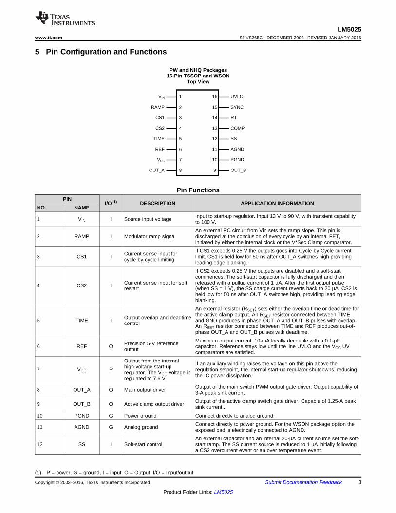
5 Pin Configuration and Functions
PW and NHQ Packages16-Pin TSSOP and WSON
Top View
Pin FunctionsPIN
I/O (1) DESCRIPTION APPLICATION INFORMATIONNO. NAME
Input to start-up regulator. Input 13 V to 90 V, with transient capability1 VIN I Source input voltage to 100 V.An external RC circuit from Vin sets the ramp slope. This pin is
2 RAMP I Modulator ramp signal discharged at the conclusion of every cycle by an internal FET,initiated by either the internal clock or the V*Sec Clamp comparator.If CS1 exceeds 0.25 V the outputs goes into Cycle-by-Cycle currentCurrent sense input for3 CS1 I limit. CS1 is held low for 50 ns after OUT_A switches high providingcycle-by-cycle limiting leading edge blanking.If CS2 exceeds 0.25 V the outputs are disabled and a soft-startcommences. The soft-start capacitor is fully discharged and then
Current sense input for soft released with a pullup current of 1 µA. After the first output pulse4 CS2 I restart (when SS = 1 V), the SS charge current reverts back to 20 µA. CS2 isheld low for 50 ns after OUT_A switches high, providing leading edgeblanking.An external resistor (RSET) sets either the overlap time or dead time forthe active clamp output. An RSET resistor connected between TIMEOutput overlap and deadtime5 TIME I and GND produces in-phase OUT_A and OUT_B pulses with overlap.control An RSET resistor connected between TIME and REF produces out-of-phase OUT_A and OUT_B pulses with deadtime.Maximum output current: 10-mA locally decouple with a 0.1-µFPrecision 5-V reference6 REF O capacitor. Reference stays low until the line UVLO and the VCC UVoutput comparators are satisfied.
Output from the internal If an auxiliary winding raises the voltage on this pin above thehigh-voltage start-up7 VCC P regulation setpoint, the internal start-up regulator shutdowns, reducingregulator. The VCC voltage is the IC power dissipation.regulated to 7.6 VOutput of the main switch PWM output gate driver. Output capability of8 OUT_A O Main output driver 3-A peak sink current.Output of the active clamp switch gate driver. Capable of 1.25-A peak9 OUT_B O Active clamp output driver sink current..
10 PGND G Power ground Connect directly to analog ground.Connect directly to power ground. For the WSON package option the11 AGND G Analog ground exposed pad is electrically connected to AGND.An external capacitor and an internal 20-µA current source set the soft-
12 SS I Soft-start control start ramp. The SS current source is reduced to 1 µA initially followinga CS2 overcurrent event or an over temperature event.
(1) P = power, G = ground, I = input, O = Output, I/O = Input/output
Copyright © 2003–2016, Texas Instruments Incorporated Submit Documentation Feedback 3
Product Folder Links: LM5025
LM5025SNVS265C –DECEMBER 2003–REVISED JANUARY 2016 www.ti.com
Pin Functions (continued)PIN
I/O (1) DESCRIPTION APPLICATION INFORMATIONNO. NAME
Input to the pulse width An internal 5-KΩ resistor pullup is provided on this pin. The external13 COMP I modulator opto-coupler sinks current from COMP to control the PWM duty cycle.An external resistor connected from RT to ground sets the internal14 RT I Oscillator timing resistor pin oscillator frequency.The internal oscillator can be synchronized to an external clock with aOscillator UP and DOWN15 SYNC I frequency 20% lower than the internal oscillator’s free runningsynchronization input frequency. There is no constraint on the maximum sync frequency.An external voltage divider from the power source sets the shutdowncomparator levels. The comparator threshold is 2.5 V. Hysteresis is set16 UVLO I Line undervoltage shutdown by an internal current source (20 µA) that is switched on or off as theUVLO pin potential crosses the 2.5-V threshold.
6 Specifications
6.1 Absolute Maximum Ratingsover operating free-air temperature range (unless otherwise noted) (1)
MIN MAX UNITVIN to GND –0.3 100
Input voltage VVCC to GND –0.3 16
CS1, CS2 to GND –0.3 1 VAll other inputs to GND –0.3 7 VJunction temperature, TJ 150 °CStorage temperature, Tstg –55 150 °C
(1) Stresses beyond those listed under Absolute Maximum Ratings may cause permanent damage to the device. These are stress ratingsonly, which do not imply functional operation of the device at these or any other conditions beyond those indicated under RecommendedOperating Conditions. Exposure to absolute-maximum-rated conditions for extended periods may affect device reliability.
6.2 ESD RatingsVALUE UNIT
Human-body model (HBM), per ANSI/ESDA/JEDEC JS01 (2) ±2000V(ESD) Electrostatic discharge (1) V
Charged-device model (CDM), per JEDEC specification JESD22-C101 (3) ±500
(1) For detailed information on soldering plastic TSSOP and WSON packages, refer to the Packaging Data Book.(2) JEDEC document JEP155 states that 500-V HBM allows safe manufacturing with a standard ESD control process.(3) JEDEC document JEP157 states that 250-V CDM allows safe manufacturing with a standard ESD control process.
6.3 Recommended Operating Conditionsover operating free-air temperature range (unless otherwise noted)
MIN NOM MAX UNITVIN voltage 13 90 VExternal voltage applied to VCC 8 15 VOperating junction temperature –40 125 °C
4 Submit Documentation Feedback Copyright © 2003–2016, Texas Instruments Incorporated
Product Folder Links: LM5025
LM5025www.ti.com SNVS265C –DECEMBER 2003–REVISED JANUARY 2016
6.4 Thermal InformationLM5025
THERMAL METRIC (1) PW (TSSOP) NHQ (WSON) UNIT16-PINS 16-PINS
RθJA Junction-to-ambient thermal resistance 98.7 30 °C/WRθJC(top) Junction-to-case (top) thermal resistance 27.8 25.9 °C/WRθJB Junction-to-board thermal resistance 44.3 9.3 °C/WψJT Junction-to-top characterization parameter 1.2 0.2 °C/WψJB Junction-to-board characterization parameter 43.6 9.5 °C/WRθJC(bot) Junction-to-case (bottom) thermal resistance — 2.3 °C/W
(1) For more information about traditional and new thermal metrics, see the Semiconductor and IC Package Thermal Metrics applicationreport, SPRA953.
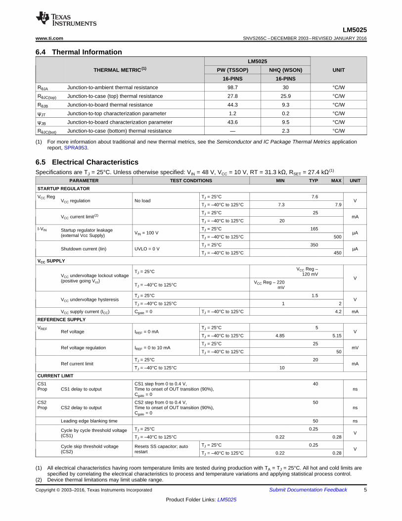
6.5 Electrical CharacteristicsSpecifications are TJ = 25°C. Unless otherwise specified: VIN = 48 V, VCC = 10 V, RT = 31.3 kΩ, RSET = 27.4 kΩ (1)
PARAMETER TEST CONDITIONS MIN TYP MAX UNIT
STARTUP REGULATOR
VCC Reg TJ = 25°C 7.6VCC regulation No load V
TJ = –40°C to 125°C 7.3 7.9
TJ = 25°C 25VCC current limit (2) mA
TJ = –40°C to 125°C 20
I-VIN TJ = 25°C 165Startup regulator leakage VIN = 100 V µA(external Vcc Supply) TJ = –40°C to 125°C 500
TJ = 25°C 350Shutdown current (Iin) UVLO = 0 V µA
TJ = –40°C to 125°C 450
VCC SUPPLY
VCC Reg –TJ = 25°C 120 mVVCC undervoltage lockout voltage V(positive going Vcc) VCC Reg – 220TJ = –40°C to 125°C mV
TJ = 25°C 1.5VCC undervoltage hysteresis V
TJ = –40°C to 125°C 1 2
VCC supply current (ICC) Cgate = 0 TJ = –40°C to 125°C 4.2 mA
REFERENCE SUPPLY
VREF TJ = 25°C 5Ref voltage IREF = 0 mA V
TJ = –40°C to 125°C 4.85 5.15
TJ = 25°C 25Ref voltage regulation IREF = 0 to 10 mA mV
TJ = –40°C to 125°C 50
TJ = 25°C 20Ref current limit mA
TJ = –40°C to 125°C 10
CURRENT LIMIT
CS1 CS1 step from 0 to 0.4 V, 40Prop CS1 delay to output Time to onset of OUT transition (90%), ns
Cgate = 0
CS2 CS2 step from 0 to 0.4 V, 50Prop CS2 delay to output Time to onset of OUT transition (90%), ns
Cgate = 0
Leading edge blanking time 50 ns
TJ = 25°C 0.25Cycle by cycle threshold voltage V(CS1) TJ = –40°C to 125°C 0.22 0.28
TJ = 25°C 0.25Cycle skip threshold voltage Resets SS capacitor; auto V(CS2) restart TJ = –40°C to 125°C 0.22 0.28
(1) All electrical characteristics having room temperature limits are tested during production with TA = TJ = 25°C. All hot and cold limits arespecified by correlating the electrical characteristics to process and temperature variations and applying statistical process control.
(2) Device thermal limitations may limit usable range.
Copyright © 2003–2016, Texas Instruments Incorporated Submit Documentation Feedback 5
Product Folder Links: LM5025
LM5025SNVS265C –DECEMBER 2003–REVISED JANUARY 2016 www.ti.com
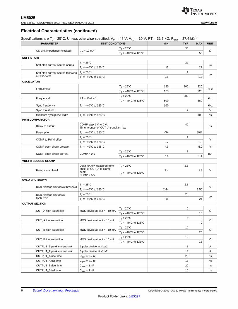
Electrical Characteristics (continued)Specifications are TJ = 25°C. Unless otherwise specified: VIN = 48 V, VCC = 10 V, RT = 31.3 kΩ, RSET = 27.4 kΩ(1)
PARAMETER TEST CONDITIONS MIN TYP MAX UNIT
TJ = 25°C 30CS sink impedance (clocked) ICS = 10 mA Ω
TJ = –40°C to 125°C 50
SOFT-START
TJ = 25°C 22Soft-start current source normal µA
TJ = –40°C to 125°C 17 27
TJ = 25°C 1Soft-start current source following µAa CS2 event TJ = –40°C to 125°C 0.5 1.5
OSCILLATOR
TJ = 25°C 180 200 220Frequency1 kHz
TJ = –40°C to 125°C 175 225
TJ = 25°C 580Frequency2 RT = 10.4 KΩ kHz
TJ = –40°C to 125°C 500 660
Sync frequency TJ = –40°C to 125°C 160 kHz
Sync threshold 2 V
Minimum sync pulse width TJ = –40°C to 125°C 100 ns
PWM COMPARATOR
COMP step 5 V to 0 V, 40Delay to output nsTime to onset of OUT_A transition low
Duty cycle TJ = –40°C to 125°C 0% 80%
TJ = 25°C 1COMP to PWM offset V
TJ = –40°C to 125°C 0.7 1.3
COMP open circuit voltage TJ = –40°C to 125°C 4.3 5.9 V
TJ = 25°C 1COMP short circuit current COMP = 0 V mA
TJ = –40°C to 125°C 0.6 1.4
VOLT × SECOND CLAMP
Delta RAMP measured from TJ = 25°C 2.5onset of OUT_A to RampRamp clamp level V2.4 2.6peak, TJ = –40°C to 125°CCOMP = 5 V
UVLO SHUTDOWN
TJ = 25°C 2.5Undervoltage shutdown threshold V
TJ = –40°C to 125°C 2.44 2.56
TJ = 25°C 20Undervoltage shutdown µAhysteresis TJ = –40°C to 125°C 16 24
OUTPUT SECTION
TJ = 25°C 5OUT_A high saturation MOS device at Iout = –10 mA Ω
TJ = –40°C to 125°C 10
TJ = 25°C 6OUT_A low saturation MOS device at Iout = 10 mA Ω
TJ = –40°C to 125°C 9
TJ = 25°C 10OUT_B high saturation MOS device at Iout = –10 mA Ω
TJ = –40°C to 125°C 20
TJ = 25°C 12OUT_B low saturation MOS device at Iout = 10 mA Ω
TJ = –40°C to 125°C 18
OUTPUT_B peak current sink Bipolar device at Vcc/2 1 A
OUTPUT_A peak current sink Bipolar device at Vcc/2 3 A
OUTPUT_A rise time Cgate = 2.2 nF 20 ns
OUTPUT_A fall time Cgate = 2.2 nF 15 ns
OUTPUT_B rise time Cgate = 1 nF 20 ns
OUTPUT_B fall time Cgate = 1 nF 15 ns
6 Submit Documentation Feedback Copyright © 2003–2016, Texas Instruments Incorporated
Product Folder Links: LM5025
LM5025www.ti.com SNVS265C –DECEMBER 2003–REVISED JANUARY 2016
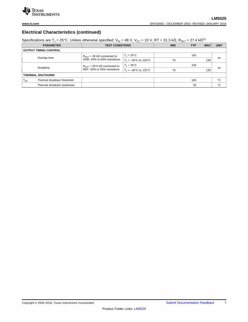
Electrical Characteristics (continued)Specifications are TJ = 25°C. Unless otherwise specified: VIN = 48 V, VCC = 10 V, RT = 31.3 kΩ, RSET = 27.4 kΩ(1)
PARAMETER TEST CONDITIONS MIN TYP MAX UNIT
OUTPUT TIMING CONTROL
TJ = 25°C 105RSET = 38 kΩ connected toOverlap time nsGND, 50% to 50% transitions TJ = –40°C to 125°C 75 135
TJ = 25°C 105RSET = 29.5 kΩ connected toDeadtime nsREF, 50% to 50% transitions TJ = –40°C to 125°C 75 135
THERMAL SHUTDOWN
TSD Thermal shutdown threshold 165 °C
Thermal shutdown hysteresis 25 °C
Copyright © 2003–2016, Texas Instruments Incorporated Submit Documentation Feedback 7
Product Folder Links: LM5025
0 20 40 60 80 100 120
RSET (k:)
0
50
100
150
200
250
300
350
400
OV
ER
LAP
TIM
E (
ns)
-40 25 75 125
TEMPERATURE (oC)
80
90
100
110
120
130
140
OV
ER
LAP
TIM
E (
ns)
RT (k:)
1 10 100
100
1000
FR
EQ
UE
NC
Y (
kH
z)
0 5 10 15 20 250
1
2
3
4
5
6
VR
EF (
V)
IREF (mA)
0 2 4 6 8 10 12 14 16
VIN (V)
0
2
4
6
8
10
12
14
16
VC
C (
V)
VIN
VCC
0 5 10 15 20 25
0
2
4
6
8
10
VC
C (
V)
ICC (mA)
LM5025SNVS265C –DECEMBER 2003–REVISED JANUARY 2016 www.ti.com
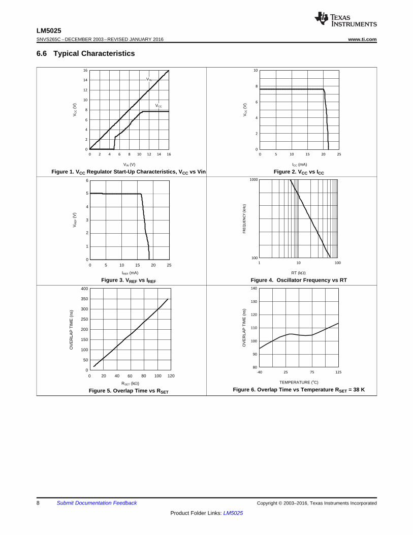
6.6 Typical Characteristics
Figure 1. VCC Regulator Start-Up Characteristics, VCC vs Vin Figure 2. VCC vs ICC
Figure 3. VREF vs IREF Figure 4. Oscillator Frequency vs RT
Figure 6. Overlap Time vs Temperature RSET = 38 KFigure 5. Overlap Time vs RSET
8 Submit Documentation Feedback Copyright © 2003–2016, Texas Instruments Incorporated
Product Folder Links: LM5025
-40 25 75 125
TEMPERATURE (oC)
14
16
18
20
22
24
26
SS
CU
RR
EN
T (P
A)
-40 25 75 125
TEMPERATURE (oC)
80
90
100
110
120
130
140
DE
AD
TIM
E (
ns)
0 20 40 60 80 100 120
RSET (k:)
0
50
100
150
200
250
300
350
400
DE
AD
TIM
E (
ns)
LM5025www.ti.com SNVS265C –DECEMBER 2003–REVISED JANUARY 2016
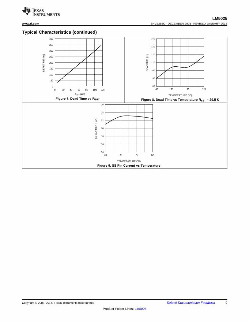
Typical Characteristics (continued)
Figure 7. Dead Time vs RSET Figure 8. Dead Time vs Temperature RSET = 29.5 K
Figure 9. SS Pin Current vs Temperature
Copyright © 2003–2016, Texas Instruments Incorporated Submit Documentation Feedback 9
Product Folder Links: LM5025
LM5025SNVS265C –DECEMBER 2003–REVISED JANUARY 2016 www.ti.com
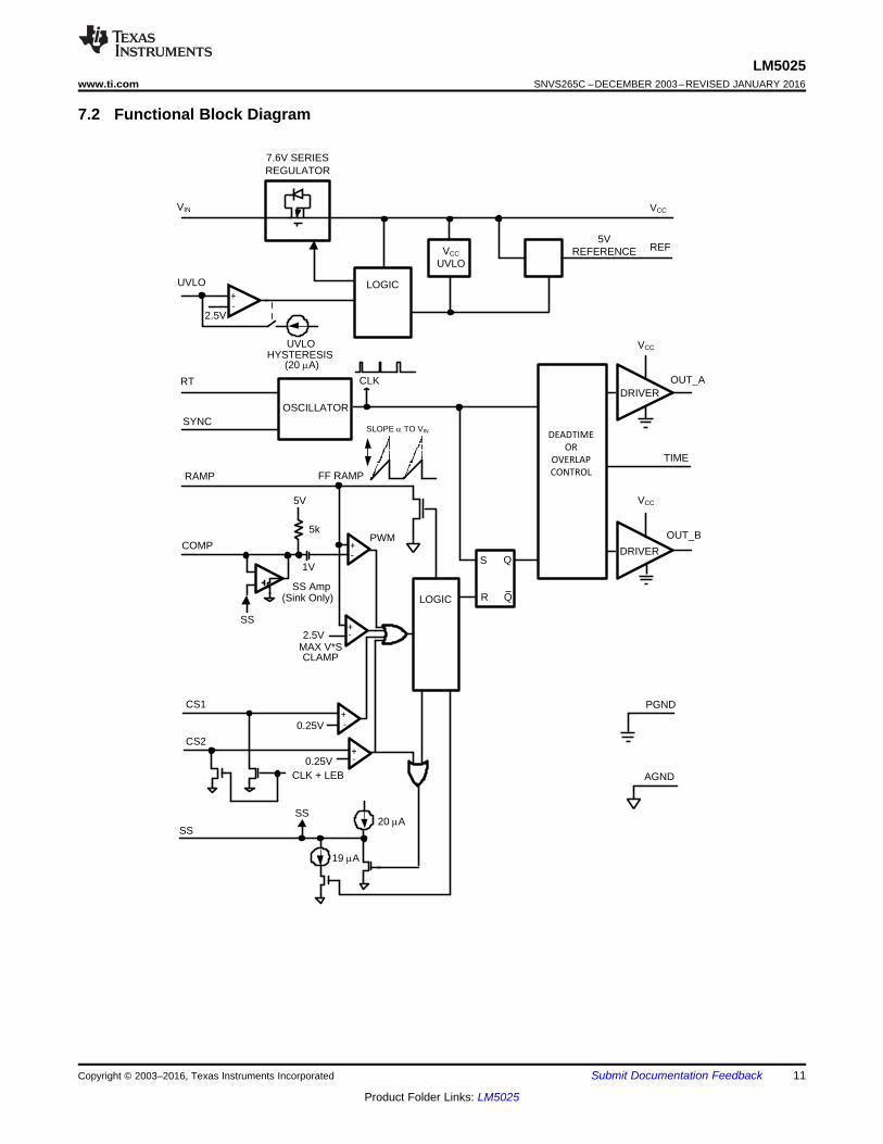
7 Detailed Description
7.1 Overview
The LM5025 PWM controller contains all of the features necessary to implement power converters using theactive clamp reset technique. The device can be configured to control either a P-channel clamp switch or anN-channel clamp switch. With the active clamp technique higher efficiencies and greater power densities can berealized compared to conventional catch winding or RDC clamp and reset techniques. Two control outputs areprovided, the main power switch control (OUT_A), and the active clamp switch control (OUT_B). The activeclamp output can be configured for either a specified overlap time (for P-channel switch applications) or aspecified dead time (for N_channel applications). The two internal compound gate drivers parallel both MOS andbipolar devices, providing superior gate-drive characteristics. This controller is designed for high-speed operationincluding an oscillator frequency range up to 1 MHz and total PWM and current sense propagation delays lessthan 100 ns. The LM5025 includes a high-voltage start-up regulator that operates over a wide input of13 V to 90 V. Additional features include: line undervoltage lockout (UVLO), soft-start, oscillator UP and DOWNsync capability, precision reference and thermal shutdown.
10 Submit Documentation Feedback Copyright © 2003–2016, Texas Instruments Incorporated
Product Folder Links: LM5025
LOGIC
VIN
REF
SS20 PA
RT
LOGIC
PGND
AGND
5V REFERENCE
OSCILLATOR
CLK
CS1
TIME
0.25V
0.25V
PWM5k
5V
1V
R
S
Q
Q
SS
FF RAMP
CS2
RAMP
SLOPE D TO VIN
CLK + LEB
7.6V SERIESREGULATOR
OUT_B
DRIVER
VCC
COMP
SS
SS Amp(Sink Only)
MAX V*SCLAMP
SYNC
UVLOHYSTERESIS
(20 PA)
2.5V
+
-
UVLO+
-
OUT_ADRIVER
VCC
VCC
VCC
UVLO
2.5V
19 PA
DEADTIME
OR
OVERLAP
CONTROL
+-
+
-
+-
LM5025www.ti.com SNVS265C –DECEMBER 2003–REVISED JANUARY 2016
7.2 Functional Block Diagram
Copyright © 2003–2016, Texas Instruments Incorporated Submit Documentation Feedback 11
Product Folder Links: LM5025
LM5025SNVS265C –DECEMBER 2003–REVISED JANUARY 2016 www.ti.com
7.3 Feature Description
7.3.1 High-Voltage Start-Up RegulatorThe LM5025 contains an internal high-voltage start-up regulator that allows the input pin (VIN) to be connecteddirectly to the line voltage. The regulator output is internally current limited to 20 mA. When power is applied, theregulator is enabled and sources current into an external capacitor connected to the VCC pin. The recommendedcapacitance for the VCC regulator is 0.1 µF to 100 µF. When the voltage on the VCC pin reaches the regulationpoint of 7.6 V and the internal voltage reference (REF) reaches its regulation point of 5 V, the controller outputsare enabled. The outputs remains enabled until VCC falls below 6.2 V or the line undervoltage lock out detectorindicates that VIN is out of range. In typical applications, an auxiliary transformer winding is connected through adiode to the VCC pin. This winding must raise the VCC voltage above 8 V to shut off the internal start-up regulator.Powering VCC from an auxiliary winding improves efficiency while reducing the controller power dissipation.
The external VCC capacitor must be sized such that the capacitor and VCC self-bias maintains a VCC voltagegreater than 6.2 V during the initial start-up. During a fault mode when the converter auxiliary winding is inactive,external current draw on the VCC line must be limited so the power dissipated in the start-up regulator does notexceed the maximum power dissipation of the controller.
An external start-up regulator or other bias rail can be used instead of the internal start-up regulator byconnecting the VCC and the VIN pins together and feeding the external bias voltage into the two pins.
7.3.2 Line Undervoltage DetectorThe LM5025 contains a line undervoltage lock out (UVLO) circuit. An external set-point voltage divider from Vinto GND, sets the operational range of the converter. The divider must be designed such that the voltage at theUVLO pin is greater than 2.5 V when Vin is in the desired operating range. If the undervoltage threshold is notmet, all functions of the controller are disabled and the controller remains in a low-power standby state. UVLOhysteresis is accomplished with an internal 20-µA current source that is switched on or off into the impedance ofthe set-point divider. When the UVLO threshold is exceeded, the current source is activated to instantly raise thevoltage at the UVLO pin. When the UVLO pin voltage falls below the 2.5-V threshold, the current source is turnedoff, causing the voltage at the UVLO pin to fall. The UVLO pin can also be used to implement a remote enableand disable function. Pulling the UVLO pin below the 2.5-V threshold disables the converter.
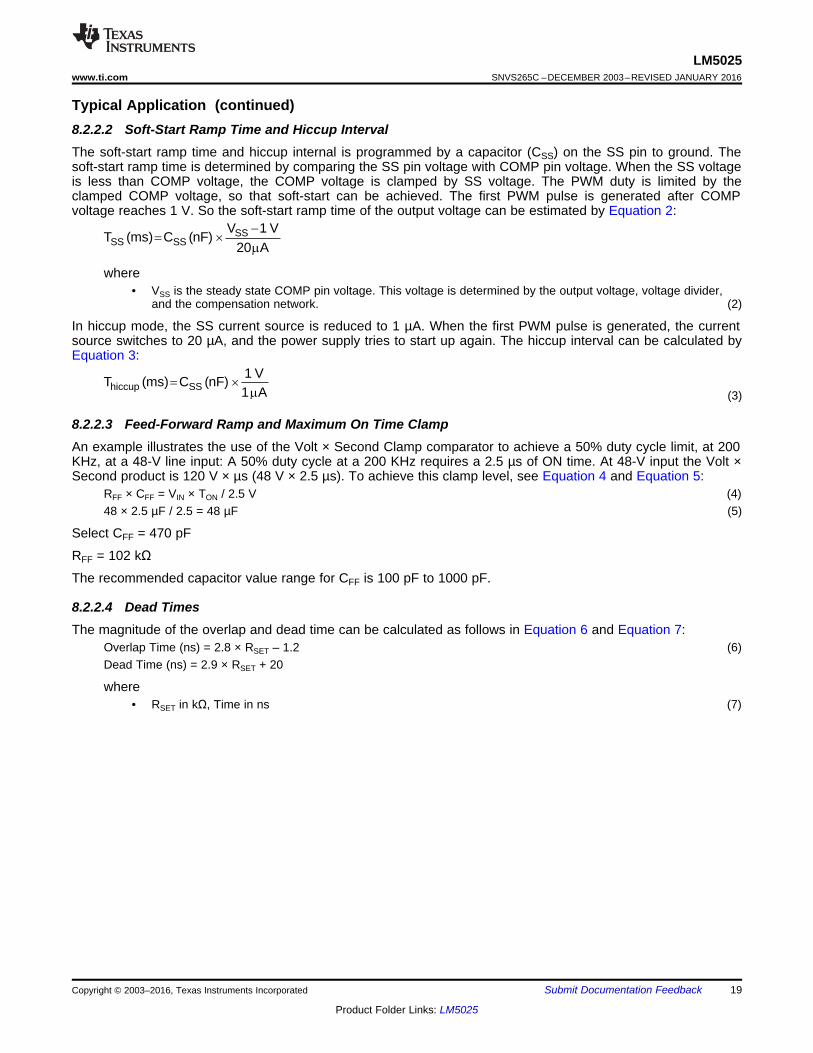
7.3.3 PWM OutputsThe relative phase of the main (OUT_A) and active clamp outputs (OUT_B) can be configured for the specificapplication. For active clamp configurations using a ground referenced P-channel clamp switch, the two outputsmust be in phase with the active clamp output overlapping the main output. For active clamp configurations usinga high side N-channel switch, the active clamp output must be out of phase with main output and there must be adead time between the two gate drive pulses. A distinguishing feature of the LM5025 is the ability to accuratelyconfigure either dead time (both off) or overlap time (both on) of the gate driver outputs. The overlap anddeadtime magnitude is controlled by the resistor value connected to the TIME pin of the controller. The oppositeend of the resistor can be connected to either REF for deadtime control or GND for overlap control. The internalconfiguration detector senses the connection and configures the phase relationship of the main and active clampoutputs.
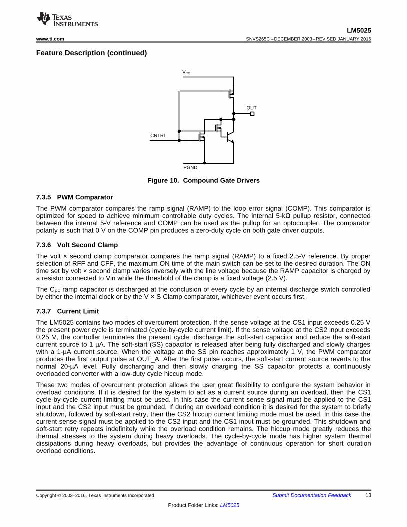
7.3.4 Compound Gate DriversThe LM5025 contains two unique compound gate drivers, which parallel both MOS and bipolar devices toprovide high-drive current throughout the entire switching event. The bipolar device provides most of the drivecurrent capability and provides a relatively constant sink current that is ideal for driving large power MOSFETs.As the switching event nears conclusion and the bipolar device saturates, the internal MOS device continues toprovide a low-impedance to compete the switching event.
During turnoff at the Miller plateau region, typically around 2 V to 3 V, is where gate driver current capability isneeded most. The resistive characteristics of all MOS gate drivers are adequate for turnon, because the supplyto output voltage differential is fairly large at the Miller region. During turnoff however, the voltage differential issmall and the current source characteristic of the bipolar gate driver is beneficial to provide fast drive capability.
12 Submit Documentation Feedback Copyright © 2003–2016, Texas Instruments Incorporated
Product Folder Links: LM5025
VCC
PGND
CNTRL
OUT
LM5025www.ti.com SNVS265C –DECEMBER 2003–REVISED JANUARY 2016
Feature Description (continued)
Figure 10. Compound Gate Drivers
7.3.5 PWM ComparatorThe PWM comparator compares the ramp signal (RAMP) to the loop error signal (COMP). This comparator isoptimized for speed to achieve minimum controllable duty cycles. The internal 5-kΩ pullup resistor, connectedbetween the internal 5-V reference and COMP can be used as the pullup for an optocoupler. The comparatorpolarity is such that 0 V on the COMP pin produces a zero-duty cycle on both gate driver outputs.
7.3.6 Volt Second ClampThe volt × second clamp comparator compares the ramp signal (RAMP) to a fixed 2.5-V reference. By properselection of RFF and CFF, the maximum ON time of the main switch can be set to the desired duration. The ONtime set by volt × second clamp varies inversely with the line voltage because the RAMP capacitor is charged bya resistor connected to Vin while the threshold of the clamp is a fixed voltage (2.5 V).
The CFF ramp capacitor is discharged at the conclusion of every cycle by an internal discharge switch controlledby either the internal clock or by the V × S Clamp comparator, whichever event occurs first.
7.3.7 Current LimitThe LM5025 contains two modes of overcurrent protection. If the sense voltage at the CS1 input exceeds 0.25 Vthe present power cycle is terminated (cycle-by-cycle current limit). If the sense voltage at the CS2 input exceeds0.25 V, the controller terminates the present cycle, discharge the soft-start capacitor and reduce the soft-startcurrent source to 1 µA. The soft-start (SS) capacitor is released after being fully discharged and slowly chargeswith a 1-µA current source. When the voltage at the SS pin reaches approximately 1 V, the PWM comparatorproduces the first output pulse at OUT_A. After the first pulse occurs, the soft-start current source reverts to thenormal 20-µA level. Fully discharging and then slowly charging the SS capacitor protects a continuouslyoverloaded converter with a low-duty cycle hiccup mode.
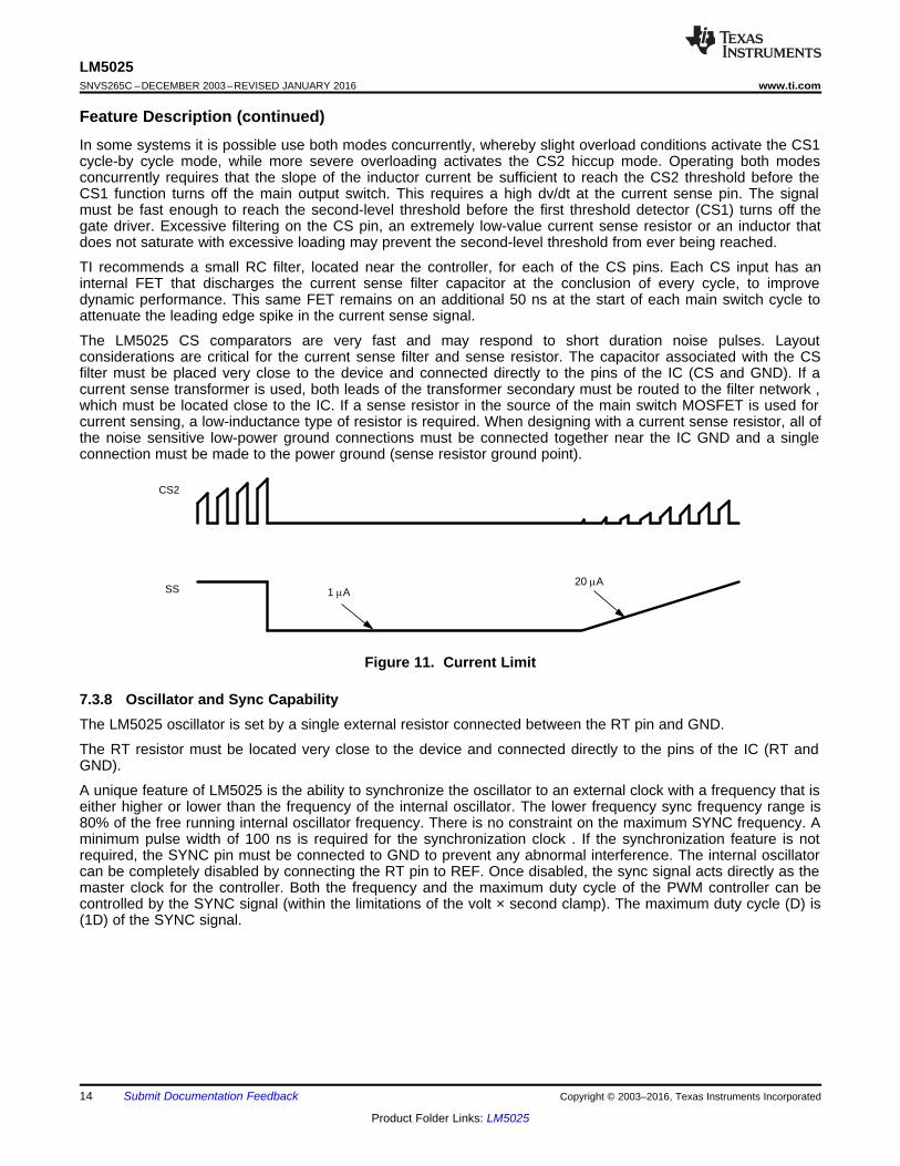
These two modes of overcurrent protection allows the user great flexibility to configure the system behavior inoverload conditions. If it is desired for the system to act as a current source during an overload, then the CS1cycle-by-cycle current limiting must be used. In this case the current sense signal must be applied to the CS1input and the CS2 input must be grounded. If during an overload condition it is desired for the system to brieflyshutdown, followed by soft-start retry, then the CS2 hiccup current limiting mode must be used. In this case thecurrent sense signal must be applied to the CS2 input and the CS1 input must be grounded. This shutdown andsoft-start retry repeats indefinitely while the overload condition remains. The hiccup mode greatly reduces thethermal stresses to the system during heavy overloads. The cycle-by-cycle mode has higher system thermaldissipations during heavy overloads, but provides the advantage of continuous operation for short durationoverload conditions.
Copyright © 2003–2016, Texas Instruments Incorporated Submit Documentation Feedback 13
Product Folder Links: LM5025
CS2
SS20 PA
1 PA
LM5025SNVS265C –DECEMBER 2003–REVISED JANUARY 2016 www.ti.com
Feature Description (continued)In some systems it is possible use both modes concurrently, whereby slight overload conditions activate the CS1cycle-by cycle mode, while more severe overloading activates the CS2 hiccup mode. Operating both modesconcurrently requires that the slope of the inductor current be sufficient to reach the CS2 threshold before theCS1 function turns off the main output switch. This requires a high dv/dt at the current sense pin. The signalmust be fast enough to reach the second-level threshold before the first threshold detector (CS1) turns off thegate driver. Excessive filtering on the CS pin, an extremely low-value current sense resistor or an inductor thatdoes not saturate with excessive loading may prevent the second-level threshold from ever being reached.
TI recommends a small RC filter, located near the controller, for each of the CS pins. Each CS input has aninternal FET that discharges the current sense filter capacitor at the conclusion of every cycle, to improvedynamic performance. This same FET remains on an additional 50 ns at the start of each main switch cycle toattenuate the leading edge spike in the current sense signal.
The LM5025 CS comparators are very fast and may respond to short duration noise pulses. Layoutconsiderations are critical for the current sense filter and sense resistor. The capacitor associated with the CSfilter must be placed very close to the device and connected directly to the pins of the IC (CS and GND). If acurrent sense transformer is used, both leads of the transformer secondary must be routed to the filter network ,which must be located close to the IC. If a sense resistor in the source of the main switch MOSFET is used forcurrent sensing, a low-inductance type of resistor is required. When designing with a current sense resistor, all ofthe noise sensitive low-power ground connections must be connected together near the IC GND and a singleconnection must be made to the power ground (sense resistor ground point).
Figure 11. Current Limit
7.3.8 Oscillator and Sync CapabilityThe LM5025 oscillator is set by a single external resistor connected between the RT pin and GND.
The RT resistor must be located very close to the device and connected directly to the pins of the IC (RT andGND).
A unique feature of LM5025 is the ability to synchronize the oscillator to an external clock with a frequency that iseither higher or lower than the frequency of the internal oscillator. The lower frequency sync frequency range is80% of the free running internal oscillator frequency. There is no constraint on the maximum SYNC frequency. Aminimum pulse width of 100 ns is required for the synchronization clock . If the synchronization feature is notrequired, the SYNC pin must be connected to GND to prevent any abnormal interference. The internal oscillatorcan be completely disabled by connecting the RT pin to REF. Once disabled, the sync signal acts directly as themaster clock for the controller. Both the frequency and the maximum duty cycle of the PWM controller can becontrolled by the SYNC signal (within the limitations of the volt × second clamp). The maximum duty cycle (D) is(1D) of the SYNC signal.
14 Submit Documentation Feedback Copyright © 2003–2016, Texas Instruments Incorporated
Product Folder Links: LM5025
LM5025www.ti.com SNVS265C –DECEMBER 2003–REVISED JANUARY 2016
Feature Description (continued)7.3.9 Feed-Forward RampAn external resistor (RFF) and capacitor (CFF) connected to VIN and GND are required to create the PWM rampsignal. The slope of the signal at the RAMP pin varies in proportion to the input line voltage. This varying slopeprovides line feedforward information necessary to improve line transient response with voltage mode control.The RAMP signal is compared to the error signal at the COMP pin by the pulse width modulator comparator tocontrol the duty cycle of the main switch output. The volt second clamp comparator also monitors the RAMP pinand if the ramp amplitude exceeds 2.5 V the present cycle is terminated. The ramp signal is reset to GND at theend of each cycle by either the internal clock or the volt second comparator, whichever occurs first.
7.3.10 Soft-StartThe soft-start feature allows the power converter to gradually reach the initial steady state operating point, thusreducing start-up stresses and surges. At power on, a 20-µA current is sourced out of the soft-start pin (SS) intoan external capacitor. The capacitor voltage ramps up slowly and limits the COMP pin voltage and therefore thePWM duty cycle. In the event of a fault as determined by VCC undervoltage, line undervoltage (UVLO), orsecond-level current limit, the output gate drivers are disabled and the soft-start capacitor is fully discharged.When the fault condition is no longer present a soft-start sequence is initiated. Following a second-level currentlimit detection (CS2), the soft-start current source is reduced to 1 µA until the first output pulse is generated bythe PWM comparator. The current source returns to the nominal 20-µA level after the first output pulse(approximately 1 V at the SS pin).
7.3.11 Thermal ProtectionInternal thermal shutdown circuitry is provided to protect the integrated circuit in the event the maximum junctiontemperature is exceeded. When activated, typically at 165°C, the controller is forced into a low-power standbystate with the output drivers and the bias regulator disabled. The device restarts after the thermal hysteresis(typically 25°C). During a restart after thermal shutdown, the soft-start capacitor is fully discharged and thencharged in the low-current mode (1 µA) similar to a second-level current limit event. The thermal protectionfeature is provided to prevent catastrophic failures from accidental device overheating.
Copyright © 2003–2016, Texas Instruments Incorporated Submit Documentation Feedback 15
Product Folder Links: LM5025
UVLO
Soft Start
Thermal Shut Down
CBC
Hiccup
Normal Operation
LM5025SNVS265C –DECEMBER 2003–REVISED JANUARY 2016 www.ti.com
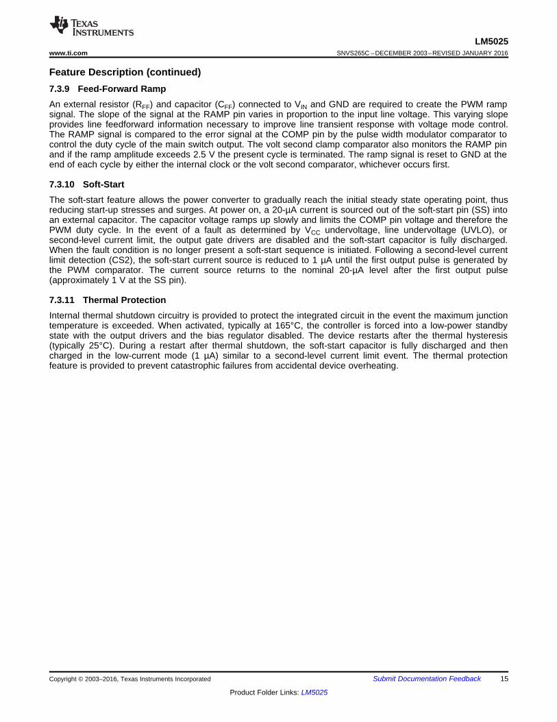
7.4 Device Functional ModesThe LM5025 active clamp voltage mode PWM controller has six functional modes. The modes transition diagramis shown in Figure 12.
• UVLO Mode• Soft-Start Mode• Normal Operation Mode• Cycle-by-Cycle Current Limit Mode• Hiccup Mode• Thermal Shut Down Mode
Figure 12. Functional Mode Transition Diagram
16 Submit Documentation Feedback Copyright © 2003–2016, Texas Instruments Incorporated
Product Folder Links: LM5025
LM5025www.ti.com SNVS265C –DECEMBER 2003–REVISED JANUARY 2016
8 Application and Implementation
NOTEInformation in the following applications sections is not part of the TI componentspecification, and TI does not warrant its accuracy or completeness. TI’s customers areresponsible for determining suitability of components for their purposes. Customers mustvalidate and test their design implementation to confirm system functionality.
8.1 Application InformationThe LM5025 PWM controller contains all of the features necessary to implement power converters using theactive clamp and reset technique. This section provides design guidance for a typical active clamp forwardconverter design. An actual application schematic of a 36-V to 78-V input, 3.3-V, 30-A output active clampforward converter is also provided in Figure 21.
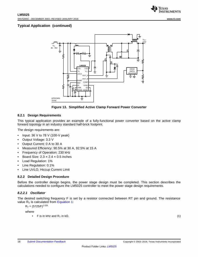
8.2 Typical ApplicationFigure 13 shows a simplified schematic of an active clamp forward power converter.
Power converters based on the forward topology offer high-efficiency and good power-handling capability inapplications up to several hundred Watts. The operation of the transformer in a forward topology does notinherently self-reset each power switching cycle, a mechanism to reset the transformer is required. The activeclamp reset mechanism is presently finding extensive use in medium-level power converters in the 50 W to200 W range.
The forward converter is derived from the Buck topology family, employing a single modulating power switch.The main difference between the topologies is the forward topology employs a transformer to provide input andoutput ground isolation and a step down or step up function.
Each cycle, the main primary switch turns on and applies the input voltage across the primary winding. Thetransformer turns the voltage to a lower-level on the secondary side. The clamp capacitor along with the resetswitch reverse biases the transformer primary each cycle when the main switch turns off. This reverse voltageresets the transformer. The clamp capacitor voltage is VIN / (1-D).
The secondary rectification employs self-driven synchronous rectification to maintain high-efficiency and ease ofdrive.
Feedback from the output is processed by an amplifier and reference, generating an error voltage, which iscoupled back to the primary side control through an opto-coupler. The LM5025 voltage mode controller pulsewidth modulates the error signal with a ramp signal derived from the input voltage. Deriving the ramp signal slopefrom the input voltage provides line feed-forward, which improves line transient rejection. The LM5025 alsoprovides a controlled delay necessary for the reset switch.
Copyright © 2003–2016, Texas Instruments Incorporated Submit Documentation Feedback 17
Product Folder Links: LM5025
LM5025
UVLO
PGND AGND
COMP
OUT_A
OUT_B
VCC
SSRt SYNC
REF
TIME
RAMP
CS1
VIN
CS2
VIN
35 - 78V
VOUT
3.3V
UP/DOWNSYNC
ERROR
AMP &
ISOLATION
LM5025SNVS265C –DECEMBER 2003–REVISED JANUARY 2016 www.ti.com
Typical Application (continued)
Figure 13. Simplified Active Clamp Forward Power Converter
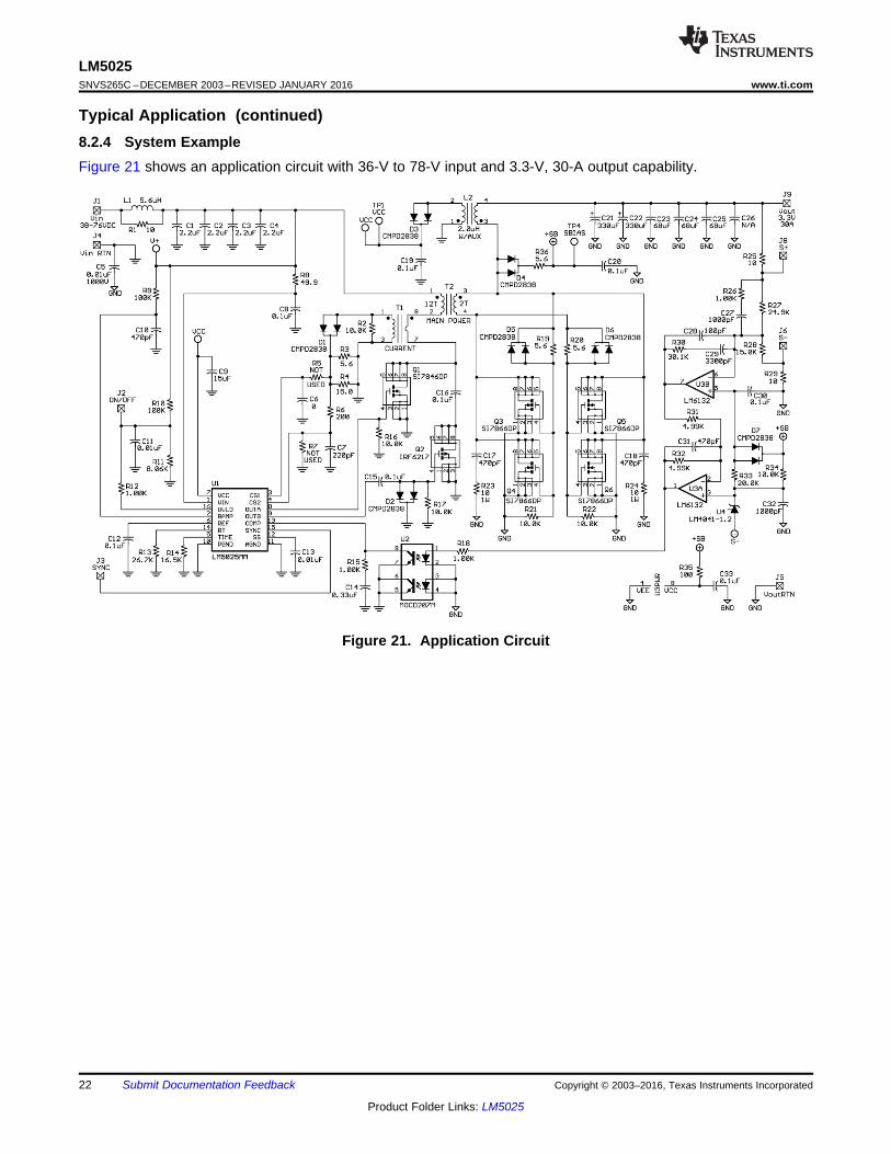
8.2.1 Design RequirementsThis typical application provides an example of a fully-functional power converter based on the active clampforward topology in an industry standard half-brick footprint.
The design requirements are:
• Input: 36 V to 78 V (100-V peak)• Output Voltage: 3.3 V• Output Current: 0 A to 30 A• Measured Efficiency: 90.5% at 30 A, 92.5% at 15 A• Frequency of Operation: 230 kHz• Board Size: 2.3 × 2.4 × 0.5 inches• Load Regulation: 1%• Line Regulation: 0.1%• Line UVLO, Hiccup Current Limit
8.2.2 Detailed Design ProcedureBefore the controller design begins, the power stage design must be completed. This section describes thecalculations needed to configure the LM5025 controller to meet the power stage design requirements.
8.2.2.1 OscillatorThe desired switching frequency F is set by a resistor connected between RT pin and ground. The resistancevalue RT is calculated from Equation 1:
RT = (5725/F)1.026
where• F is in kHz and RT in kΩ. (1)
18 Submit Documentation Feedback Copyright © 2003–2016, Texas Instruments Incorporated
Product Folder Links: LM5025
hiccup SS1 V
T (ms) C (nF)1 A
uP
SSSS SS
V 1 VT (ms) C (nF)
20 A
u
P
LM5025www.ti.com SNVS265C –DECEMBER 2003–REVISED JANUARY 2016
Typical Application (continued)8.2.2.2 Soft-Start Ramp Time and Hiccup IntervalThe soft-start ramp time and hiccup internal is programmed by a capacitor (CSS) on the SS pin to ground. Thesoft-start ramp time is determined by comparing the SS pin voltage with COMP pin voltage. When the SS voltageis less than COMP voltage, the COMP voltage is clamped by SS voltage. The PWM duty is limited by theclamped COMP voltage, so that soft-start can be achieved. The first PWM pulse is generated after COMPvoltage reaches 1 V. So the soft-start ramp time of the output voltage can be estimated by Equation 2:
where• VSS is the steady state COMP pin voltage. This voltage is determined by the output voltage, voltage divider,
and the compensation network. (2)
In hiccup mode, the SS current source is reduced to 1 µA. When the first PWM pulse is generated, the currentsource switches to 20 µA, and the power supply tries to start up again. The hiccup interval can be calculated byEquation 3:
(3)
8.2.2.3 Feed-Forward Ramp and Maximum On Time ClampAn example illustrates the use of the Volt × Second Clamp comparator to achieve a 50% duty cycle limit, at 200KHz, at a 48-V line input: A 50% duty cycle at a 200 KHz requires a 2.5 µs of ON time. At 48-V input the Volt ×Second product is 120 V × µs (48 V × 2.5 µs). To achieve this clamp level, see Equation 4 and Equation 5:
RFF × CFF = VIN × TON / 2.5 V (4)48 × 2.5 µF / 2.5 = 48 µF (5)
Select CFF = 470 pF
RFF = 102 kΩ
The recommended capacitor value range for CFF is 100 pF to 1000 pF.
8.2.2.4 Dead TimesThe magnitude of the overlap and dead time can be calculated as follows in Equation 6 and Equation 7:
Overlap Time (ns) = 2.8 × RSET – 1.2 (6)Dead Time (ns) = 2.9 × RSET + 20
where• RSET in kΩ, Time in ns (7)
Copyright © 2003–2016, Texas Instruments Incorporated Submit Documentation Feedback 19
Product Folder Links: LM5025
P-Channel Active Clamp(RSET to GND)
N-Channel Active Clamp(RSET to REF)
OUT_A
OUT_B
K1 x RSET
K2 x RSET
OUT_A
OUT_B
LM5025SNVS265C –DECEMBER 2003–REVISED JANUARY 2016 www.ti.com
Typical Application (continued)
Figure 14. PWM Outputs
20 Submit Documentation Feedback Copyright © 2003–2016, Texas Instruments Incorporated
Product Folder Links: LM5025
1
1
2
1
1
1 2
1
LM5025www.ti.com SNVS265C –DECEMBER 2003–REVISED JANUARY 2016
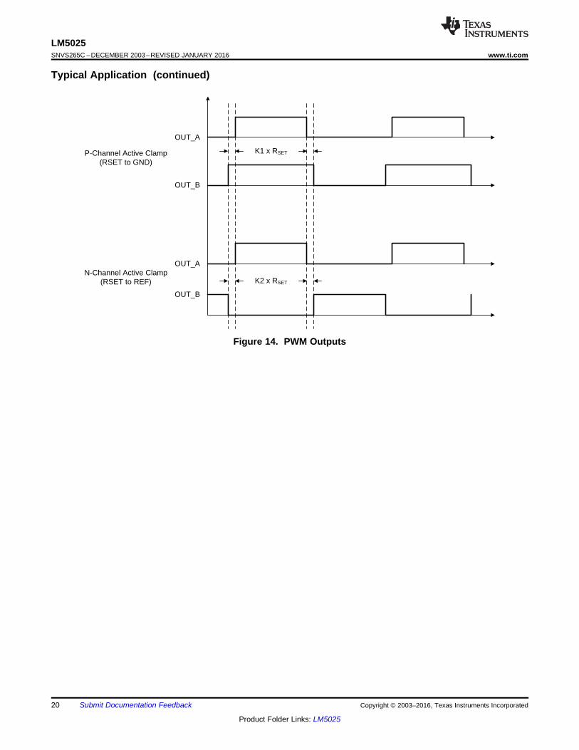
Typical Application (continued)8.2.3 Application Curves
Conditions: input voltage = 48 VDC, output current = 5 A Conditions: input voltage = 48 VDC, output current = 5 A to 25 ATrace 1: output voltage Volts/div = 0.5 V Trace 1: output voltage Volts/div = 0.5 VHorizontal resolution = 1 ms/div Trace 2: output current, Amps/div = 10 A
Horizontal resolution = 1 μs/div
Figure 15. Output Voltage During Typical Startup Figure 16. Transient Response
Conditions: input voltage = 48 VDC, output current = 30 A Conditions: input voltage = 38 VDC, output current = 25 ABandwidth limit = 25 MHz Trace 1: Q1 drain voltage Volts/div = 20 VTrace 1: output ripple voltage Volts/div = 50 mV Horizontal resolution = 1 μs/divHorizontal resolution = 2 μs/div
Figure 17. Output Ripple Figure 18. Drain Voltage
Conditions: input voltage = 78 VDC, output current = 25 A Conditions: input voltage = 48 VDC, output current = 5 ATrace 1: Q1 drain voltage Volts/div = 20 V Synchronous rectifier, Q3 gate Volts/div = 5 VHorizontal resolution = 1 μs/div Trace 1: synchronous rectifier, Q3 gate Volts/div = 5 V
Trace 2: synchronous rectifier, Q5 gate Volts/div = 5 VHorizontal resolution = 1 μs/div
Figure 19. Drain Voltage Figure 20. Gate Voltages of the Synchronous Rectifiers
Copyright © 2003–2016, Texas Instruments Incorporated Submit Documentation Feedback 21
Product Folder Links: LM5025
LM5025SNVS265C –DECEMBER 2003–REVISED JANUARY 2016 www.ti.com
Typical Application (continued)8.2.4 System ExampleFigure 21 shows an application circuit with 36-V to 78-V input and 3.3-V, 30-A output capability.
Figure 21. Application Circuit
22 Submit Documentation Feedback Copyright © 2003–2016, Texas Instruments Incorporated
Product Folder Links: LM5025
LM5025www.ti.com SNVS265C –DECEMBER 2003–REVISED JANUARY 2016
9 Power Supply RecommendationsVCC pin is the power supply for the device. There must be a 0.1-µF to approximately 100-μF capacitor directlyfrom VCC to ground. REF pin must be bypassed to ground as close as possible to the device using a 0.1-μFcapacitor.
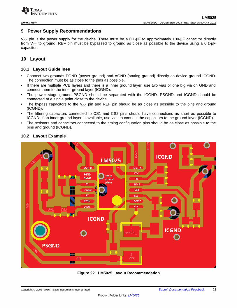
10 Layout
10.1 Layout Guidelines• Connect two grounds PGND (power ground) and AGND (analog ground) directly as device ground ICGND.
The connection must be as close to the pins as possible.• If there are multiple PCB layers and there is a inner ground layer, use two vias or one big via on GND and
connect them to the inner ground layer (ICGND).• The power stage ground PSGND should be separated with the ICGND. PSGND and ICGND should be
connected at a single point close to the device.• The bypass capacitors to the VCC pin and REF pin should be as close as possible to the pins and ground
(ICGND).• The filtering capacitors connected to CS1 and CS2 pins should have connections as short as possible to
ICGND; if an inner ground layer is available, use vias to connect the capacitors to the ground layer (ICGND).• The resistors and capacitors connected to the timing configuration pins should be as close as possible to the
pins and ground (ICGND).
10.2 Layout Example
Figure 22. LM5025 Layout Recommendation
Copyright © 2003–2016, Texas Instruments Incorporated Submit Documentation Feedback 23
Product Folder Links: LM5025
LM5025SNVS265C –DECEMBER 2003–REVISED JANUARY 2016 www.ti.com
11 Device and Documentation Support
11.1 Documentation Support
11.1.1 Related DocumentationFor related documentation, see the following:• LM5025 Isolated Active Clamp Forward Converter Ref Design User Guide, SNVU096
11.2 Community ResourcesThe following links connect to TI community resources. Linked contents are provided "AS IS" by the respectivecontributors. They do not constitute TI specifications and do not necessarily reflect TI's views; see TI's Terms ofUse.
TI E2E™ Online Community TI's Engineer-to-Engineer (E2E) Community. Created to foster collaborationamong engineers. At e2e.ti.com, you can ask questions, share knowledge, explore ideas and helpsolve problems with fellow engineers.
Design Support TI's Design Support Quickly find helpful E2E forums along with design support tools andcontact information for technical support.
11.3 TrademarksE2E is a trademark of Texas Instruments.All other trademarks are the property of their respective owners.
11.4 Electrostatic Discharge CautionThese devices have limited built-in ESD protection. The leads should be shorted together or the device placed in conductive foamduring storage or handling to prevent electrostatic damage to the MOS gates.
11.5 GlossarySLYZ022 — TI Glossary.
This glossary lists and explains terms, acronyms, and definitions.
12 Mechanical, Packaging, and Orderable InformationThe following pages include mechanical, packaging, and orderable information. This information is the mostcurrent data available for the designated devices. This data is subject to change without notice and revision ofthis document. For browser-based versions of this data sheet, refer to the left-hand navigation.
24 Submit Documentation Feedback Copyright © 2003–2016, Texas Instruments Incorporated
Product Folder Links: LM5025
PACKAGE OPTION ADDENDUM
www.ti.com 13-Oct-2015
Addendum-Page 1
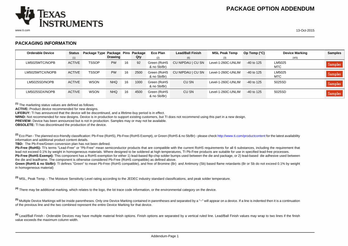
PACKAGING INFORMATION
Orderable Device Status(1)
Package Type PackageDrawing
Pins PackageQty
Eco Plan(2)
Lead/Ball Finish(6)
MSL Peak Temp(3)
Op Temp (°C) Device Marking(4/5)
Samples
LM5025MTC/NOPB ACTIVE TSSOP PW 16 92 Green (RoHS& no Sb/Br)
CU NIPDAU | CU SN Level-1-260C-UNLIM -40 to 125 LM5025MTC
LM5025MTCX/NOPB ACTIVE TSSOP PW 16 2500 Green (RoHS& no Sb/Br)
CU NIPDAU | CU SN Level-1-260C-UNLIM -40 to 125 LM5025MTC
LM5025SD/NOPB ACTIVE WSON NHQ 16 1000 Green (RoHS& no Sb/Br)
CU SN Level-1-260C-UNLIM -40 to 125 5025SD
LM5025SDX/NOPB ACTIVE WSON NHQ 16 4500 Green (RoHS& no Sb/Br)
CU SN Level-1-260C-UNLIM -40 to 125 5025SD
(1) The marketing status values are defined as follows:ACTIVE: Product device recommended for new designs.LIFEBUY: TI has announced that the device will be discontinued, and a lifetime-buy period is in effect.NRND: Not recommended for new designs. Device is in production to support existing customers, but TI does not recommend using this part in a new design.PREVIEW: Device has been announced but is not in production. Samples may or may not be available.OBSOLETE: TI has discontinued the production of the device.
(2) Eco Plan - The planned eco-friendly classification: Pb-Free (RoHS), Pb-Free (RoHS Exempt), or Green (RoHS & no Sb/Br) - please check http://www.ti.com/productcontent for the latest availabilityinformation and additional product content details.TBD: The Pb-Free/Green conversion plan has not been defined.Pb-Free (RoHS): TI's terms "Lead-Free" or "Pb-Free" mean semiconductor products that are compatible with the current RoHS requirements for all 6 substances, including the requirement thatlead not exceed 0.1% by weight in homogeneous materials. Where designed to be soldered at high temperatures, TI Pb-Free products are suitable for use in specified lead-free processes.Pb-Free (RoHS Exempt): This component has a RoHS exemption for either 1) lead-based flip-chip solder bumps used between the die and package, or 2) lead-based die adhesive used betweenthe die and leadframe. The component is otherwise considered Pb-Free (RoHS compatible) as defined above.Green (RoHS & no Sb/Br): TI defines "Green" to mean Pb-Free (RoHS compatible), and free of Bromine (Br) and Antimony (Sb) based flame retardants (Br or Sb do not exceed 0.1% by weightin homogeneous material)
(3) MSL, Peak Temp. - The Moisture Sensitivity Level rating according to the JEDEC industry standard classifications, and peak solder temperature.
(4) There may be additional marking, which relates to the logo, the lot trace code information, or the environmental category on the device.
(5) Multiple Device Markings will be inside parentheses. Only one Device Marking contained in parentheses and separated by a "~" will appear on a device. If a line is indented then it is a continuationof the previous line and the two combined represent the entire Device Marking for that device.
(6) Lead/Ball Finish - Orderable Devices may have multiple material finish options. Finish options are separated by a vertical ruled line. Lead/Ball Finish values may wrap to two lines if the finishvalue exceeds the maximum column width.
PACKAGE OPTION ADDENDUM
www.ti.com 13-Oct-2015
Addendum-Page 2
Important Information and Disclaimer:The information provided on this page represents TI's knowledge and belief as of the date that it is provided. TI bases its knowledge and belief on informationprovided by third parties, and makes no representation or warranty as to the accuracy of such information. Efforts are underway to better integrate information from third parties. TI has taken andcontinues to take reasonable steps to provide representative and accurate information but may not have conducted destructive testing or chemical analysis on incoming materials and chemicals.TI and TI suppliers consider certain information to be proprietary, and thus CAS numbers and other limited information may not be available for release.
In no event shall TI's liability arising out of such information exceed the total purchase price of the TI part(s) at issue in this document sold by TI to Customer on an annual basis.
TAPE AND REEL INFORMATION
*All dimensions are nominal
Device PackageType
PackageDrawing
Pins SPQ ReelDiameter
(mm)
ReelWidth
W1 (mm)
A0(mm)
B0(mm)
K0(mm)
P1(mm)
W(mm)
Pin1Quadrant
LM5025MTCX/NOPB TSSOP PW 16 2500 330.0 12.4 6.95 5.6 1.6 8.0 12.0 Q1
LM5025MTCX/NOPB TSSOP PW 16 2500 330.0 12.4 6.95 5.6 1.6 8.0 12.0 Q1
LM5025SD/NOPB WSON NHQ 16 1000 178.0 12.4 5.3 5.3 1.3 8.0 12.0 Q1
LM5025SDX/NOPB WSON NHQ 16 4500 330.0 12.4 5.3 5.3 1.3 8.0 12.0 Q1
PACKAGE MATERIALS INFORMATION
www.ti.com 21-Jul-2016
Pack Materials-Page 1
*All dimensions are nominal
Device Package Type Package Drawing Pins SPQ Length (mm) Width (mm) Height (mm)
LM5025MTCX/NOPB TSSOP PW 16 2500 367.0 367.0 35.0
LM5025MTCX/NOPB TSSOP PW 16 2500 367.0 367.0 35.0
LM5025SD/NOPB WSON NHQ 16 1000 210.0 185.0 35.0
LM5025SDX/NOPB WSON NHQ 16 4500 367.0 367.0 35.0
PACKAGE MATERIALS INFORMATION
www.ti.com 21-Jul-2016
Pack Materials-Page 2
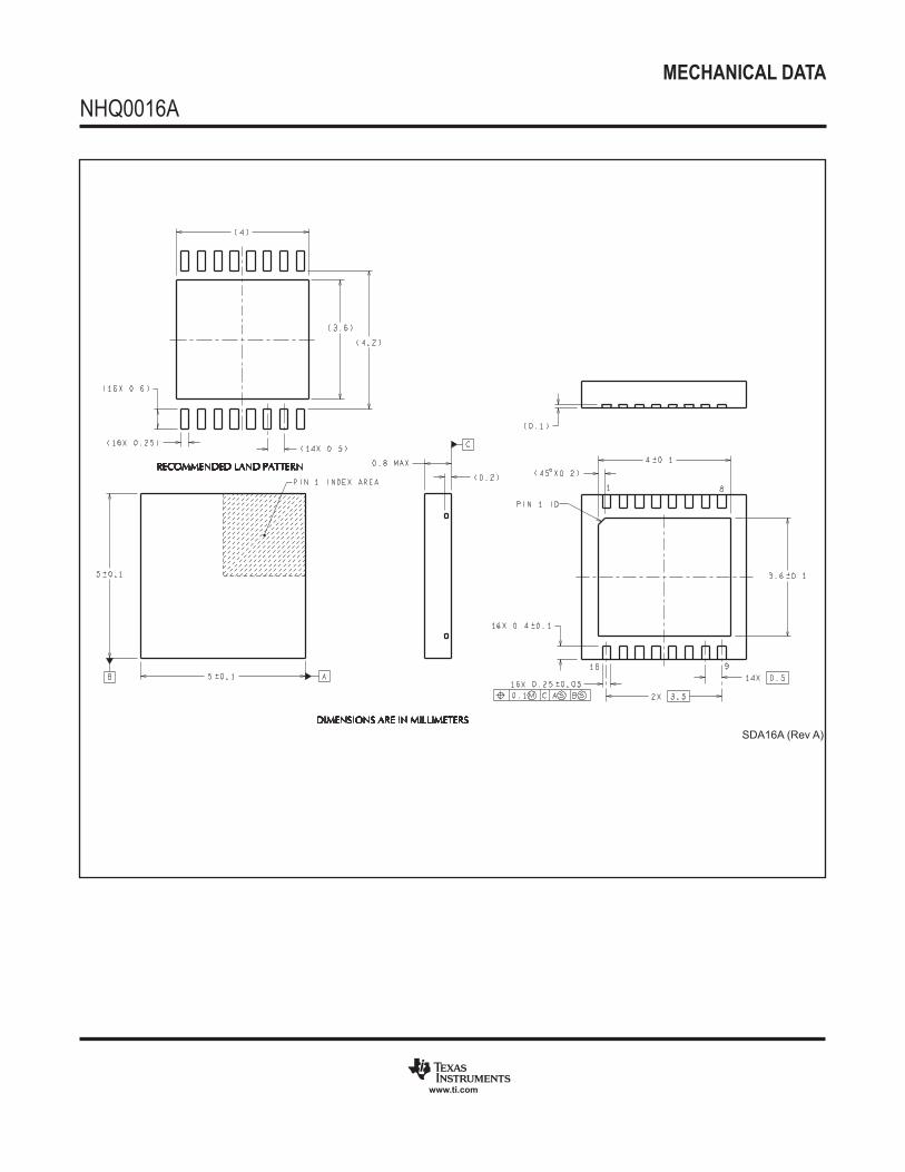
MECHANICAL DATA
NHQ0016A
www.ti.com
SDA16A (Rev A)
IMPORTANT NOTICE
Texas Instruments Incorporated and its subsidiaries (TI) reserve the right to make corrections, enhancements, improvements and otherchanges to its semiconductor products and services per JESD46, latest issue, and to discontinue any product or service per JESD48, latestissue. Buyers should obtain the latest relevant information before placing orders and should verify that such information is current andcomplete. All semiconductor products (also referred to herein as “components”) are sold subject to TI’s terms and conditions of salesupplied at the time of order acknowledgment.TI warrants performance of its components to the specifications applicable at the time of sale, in accordance with the warranty in TI’s termsand conditions of sale of semiconductor products. Testing and other quality control techniques are used to the extent TI deems necessaryto support this warranty. Except where mandated by applicable law, testing of all parameters of each component is not necessarilyperformed.TI assumes no liability for applications assistance or the design of Buyers’ products. Buyers are responsible for their products andapplications using TI components. To minimize the risks associated with Buyers’ products and applications, Buyers should provideadequate design and operating safeguards.TI does not warrant or represent that any license, either express or implied, is granted under any patent right, copyright, mask work right, orother intellectual property right relating to any combination, machine, or process in which TI components or services are used. Informationpublished by TI regarding third-party products or services does not constitute a license to use such products or services or a warranty orendorsement thereof. Use of such information may require a license from a third party under the patents or other intellectual property of thethird party, or a license from TI under the patents or other intellectual property of TI.Reproduction of significant portions of TI information in TI data books or data sheets is permissible only if reproduction is without alterationand is accompanied by all associated warranties, conditions, limitations, and notices. TI is not responsible or liable for such altereddocumentation. Information of third parties may be subject to additional restrictions.Resale of TI components or services with statements different from or beyond the parameters stated by TI for that component or servicevoids all express and any implied warranties for the associated TI component or service and is an unfair and deceptive business practice.TI is not responsible or liable for any such statements.Buyer acknowledges and agrees that it is solely responsible for compliance with all legal, regulatory and safety-related requirementsconcerning its products, and any use of TI components in its applications, notwithstanding any applications-related information or supportthat may be provided by TI. Buyer represents and agrees that it has all the necessary expertise to create and implement safeguards whichanticipate dangerous consequences of failures, monitor failures and their consequences, lessen the likelihood of failures that might causeharm and take appropriate remedial actions. Buyer will fully indemnify TI and its representatives against any damages arising out of the useof any TI components in safety-critical applications.In some cases, TI components may be promoted specifically to facilitate safety-related applications. With such components, TI’s goal is tohelp enable customers to design and create their own end-product solutions that meet applicable functional safety standards andrequirements. Nonetheless, such components are subject to these terms.No TI components are authorized for use in FDA Class III (or similar life-critical medical equipment) unless authorized officers of the partieshave executed a special agreement specifically governing such use.Only those TI components which TI has specifically designated as military grade or “enhanced plastic” are designed and intended for use inmilitary/aerospace applications or environments. Buyer acknowledges and agrees that any military or aerospace use of TI componentswhich have not been so designated is solely at the Buyer's risk, and that Buyer is solely responsible for compliance with all legal andregulatory requirements in connection with such use.TI has specifically designated certain components as meeting ISO/TS16949 requirements, mainly for automotive use. In any case of use ofnon-designated products, TI will not be responsible for any failure to meet ISO/TS16949.
Products ApplicationsAudio www.ti.com/audio Automotive and Transportation www.ti.com/automotiveAmplifiers amplifier.ti.com Communications and Telecom www.ti.com/communicationsData Converters dataconverter.ti.com Computers and Peripherals www.ti.com/computersDLP® Products www.dlp.com Consumer Electronics www.ti.com/consumer-appsDSP dsp.ti.com Energy and Lighting www.ti.com/energyClocks and Timers www.ti.com/clocks Industrial www.ti.com/industrialInterface interface.ti.com Medical www.ti.com/medicalLogic logic.ti.com Security www.ti.com/securityPower Mgmt power.ti.com Space, Avionics and Defense www.ti.com/space-avionics-defenseMicrocontrollers microcontroller.ti.com Video and Imaging www.ti.com/videoRFID www.ti-rfid.comOMAP Applications Processors www.ti.com/omap TI E2E Community e2e.ti.comWireless Connectivity www.ti.com/wirelessconnectivity
Mailing Address: Texas Instruments, Post Office Box 655303, Dallas, Texas 75265Copyright © 2016, Texas Instruments Incorporated