Transistor Audio and Radio Circuits - Mullard (1 Watt amplifier)
LM4889
www.ti.com SNAS157G –MAY 2004–REVISED NOVEMBER 2006
LM4889 1 Watt Audio Power AmplifierCheck for Samples: LM4889
1FEATURES • No output coupling capacitors, snubbernetworks or bootstrap capacitors required
2• Available in space-saving MSOP, SOIC, LLP,• Unity-gain stableand micro SMD packages• External gain configuration capability• Ultra low current shutdown mode (3.3 to 2.6V -
0.01µA)APPLICATIONS• Can drive capacitive loads up to 500 pF• Mobile Phones• Improved pop & click circuitry eliminates
noises during turn-on and turn-off transitions • PDAs• 2.2 - 5.5V operation • Portable electronic devices
DESCRIPTIONThe LM4889 is an audio power amplifier primarily designed for demanding applications in mobile phones andother portable communication device applications. It is capable of delivering 1 watt of continuous average powerto an 8Ω BTL load with less than 2% distortion (THD+N) from a 5VDC power supply.
Boomer audio power amplifiers were designed specifically to provide high quality output power with a minimalamount of external components. The LM4889 does not require output coupling capacitors or bootstrapcapacitors, and therefore is ideally suited for mobile phone and other low voltage applications where minimalpower consumption is a primary requirement.
The LM4889 features a low-power consumption shutdown mode, which is achieved by driving the shutdown pinwith a logic low. Additionally, the LM4889 features an internal thermal shutdown protection mechanism.
The LM4889 contains advanced pop & click circuitry to eliminate noise which would otherwise occur during turn-on and turn-off transitions.
The LM4889 is unity-gain stable and can be configured by external gain-setting resistors.
Table 1. Key Specifications
VALUE UNIT
Improved PSRR at 217Hz, 5 - 3.3V 75 dB
Power Output at 5.0V & 2% THD 1.0 W(typ.)
Power Output at 3.3V & 1% THD 400 mW(typ.)
Shutdown Current at 3.3 & 2.6V 0.01 µA(typ.)
1
Please be aware that an important notice concerning availability, standard warranty, and use in critical applications ofTexas Instruments semiconductor products and disclaimers thereto appears at the end of this data sheet.
2All trademarks are the property of their respective owners.
PRODUCTION DATA information is current as of publication date. Copyright © 2004–2006, Texas Instruments IncorporatedProducts conform to specifications per the terms of the TexasInstruments standard warranty. Production processing does notnecessarily include testing of all parameters.
LM4889
SNAS157G –MAY 2004–REVISED NOVEMBER 2006 www.ti.com
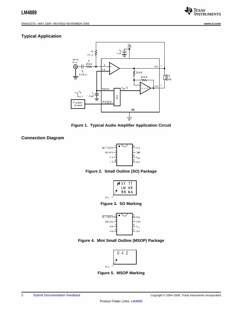
Typical Application
Figure 1. Typical Audio Amplifier Application Circuit
Connection Diagram
Figure 2. Small Outline (SO) Package
Figure 3. SO Marking
Figure 4. Mini Small Outline (MSOP) Package
Figure 5. MSOP Marking
2 Submit Documentation Feedback Copyright © 2004–2006, Texas Instruments Incorporated
Product Folder Links: LM4889
LM4889
www.ti.com SNAS157G –MAY 2004–REVISED NOVEMBER 2006
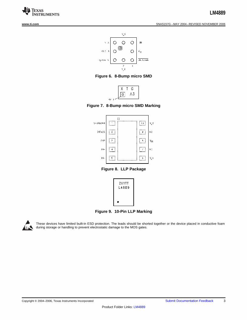
Figure 6. 8-Bump micro SMD
Figure 7. 8-Bump micro SMD Marking
Figure 8. LLP Package
Figure 9. 10-Pin LLP Marking
These devices have limited built-in ESD protection. The leads should be shorted together or the device placed in conductive foamduring storage or handling to prevent electrostatic damage to the MOS gates.
Copyright © 2004–2006, Texas Instruments Incorporated Submit Documentation Feedback 3
Product Folder Links: LM4889
LM4889
SNAS157G –MAY 2004–REVISED NOVEMBER 2006 www.ti.com
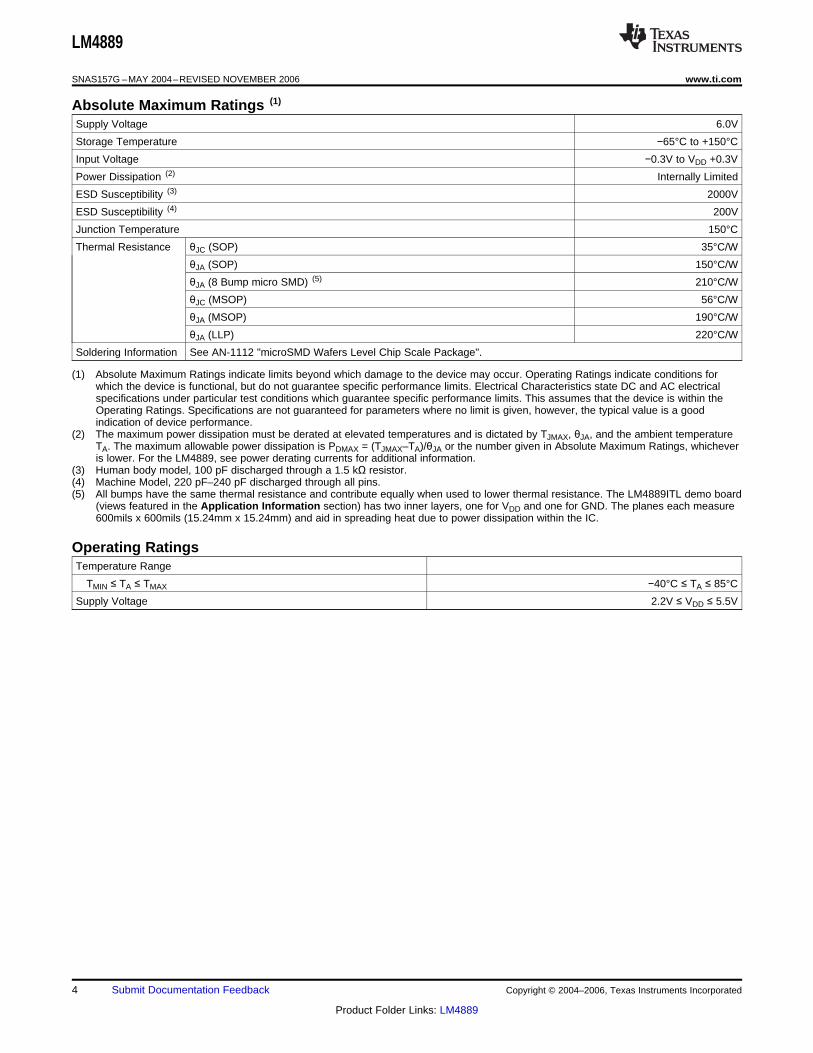
Absolute Maximum Ratings (1)
Supply Voltage 6.0V
Storage Temperature −65°C to +150°C
Input Voltage −0.3V to VDD +0.3V
Power Dissipation (2) Internally Limited
ESD Susceptibility (3) 2000V
ESD Susceptibility (4) 200V
Junction Temperature 150°C
Thermal Resistance θJC (SOP) 35°C/W
θJA (SOP) 150°C/W
θJA (8 Bump micro SMD) (5) 210°C/W
θJC (MSOP) 56°C/W
θJA (MSOP) 190°C/W
θJA (LLP) 220°C/W
Soldering Information See AN-1112 "microSMD Wafers Level Chip Scale Package".
(1) Absolute Maximum Ratings indicate limits beyond which damage to the device may occur. Operating Ratings indicate conditions forwhich the device is functional, but do not guarantee specific performance limits. Electrical Characteristics state DC and AC electricalspecifications under particular test conditions which guarantee specific performance limits. This assumes that the device is within theOperating Ratings. Specifications are not guaranteed for parameters where no limit is given, however, the typical value is a goodindication of device performance.
(2) The maximum power dissipation must be derated at elevated temperatures and is dictated by TJMAX, θJA, and the ambient temperatureTA. The maximum allowable power dissipation is PDMAX = (TJMAX–TA)/θJA or the number given in Absolute Maximum Ratings, whicheveris lower. For the LM4889, see power derating currents for additional information.
(3) Human body model, 100 pF discharged through a 1.5 kΩ resistor.(4) Machine Model, 220 pF–240 pF discharged through all pins.(5) All bumps have the same thermal resistance and contribute equally when used to lower thermal resistance. The LM4889ITL demo board
(views featured in the Application Information section) has two inner layers, one for VDD and one for GND. The planes each measure600mils x 600mils (15.24mm x 15.24mm) and aid in spreading heat due to power dissipation within the IC.
Operating RatingsTemperature Range
TMIN ≤ TA ≤ TMAX −40°C ≤ TA ≤ 85°C
Supply Voltage 2.2V ≤ VDD ≤ 5.5V
4 Submit Documentation Feedback Copyright © 2004–2006, Texas Instruments Incorporated
Product Folder Links: LM4889
LM4889
www.ti.com SNAS157G –MAY 2004–REVISED NOVEMBER 2006
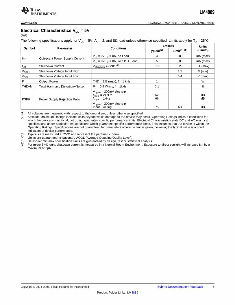
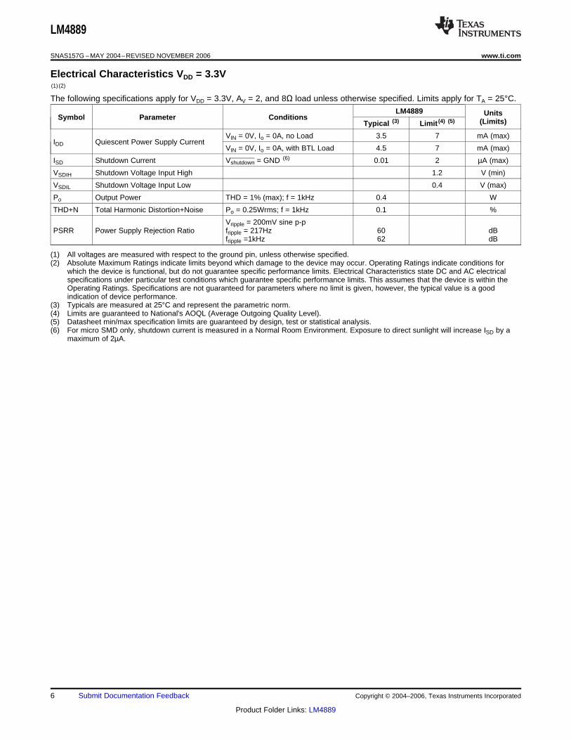
Electrical Characteristics VDD = 5V(1) (2)
The following specifications apply for VDD = 5V, AV = 2, and 8Ω load unless otherwise specified. Limits apply for TA = 25°C.
LM4889 UnitsSymbol Parameter Conditions (Limits)Typical (3) Limit (4) (5)
VIN = 0V, Io = 0A, no Load 4 8 mA (max)IDD Quiescent Power Supply Current
VIN = 0V, Io = 0A, with BTL Load 5 8 mA (max)
ISD Shutdown Current Vshutdown = GND (6) 0.1 2 µA (max)
VSDIH Shutdown Voltage Input High 1.2 V (min)
VSDIL Shutdown Voltage Input Low 0.4 V (max)
Po Output Power THD = 2% (max); f = 1 kHz 1 W
THD+N Total Harmonic Distortion+Noise Po = 0.4 Wrms; f = 1kHz 0.1 %
Vripple = 200mV sine p-pfripple = 217Hz 62 dBfripple = 1kHz 66 dBPSRR Power Supply Rejection RatioVripple = 200mV sine p-pInput Floating 75 68 dB
(1) All voltages are measured with respect to the ground pin, unless otherwise specified.(2) Absolute Maximum Ratings indicate limits beyond which damage to the device may occur. Operating Ratings indicate conditions for
which the device is functional, but do not guarantee specific performance limits. Electrical Characteristics state DC and AC electricalspecifications under particular test conditions which guarantee specific performance limits. This assumes that the device is within theOperating Ratings. Specifications are not guaranteed for parameters where no limit is given, however, the typical value is a goodindication of device performance.
(3) Typicals are measured at 25°C and represent the parametric norm.(4) Limits are guaranteed to National's AOQL (Average Outgoing Quality Level).(5) Datasheet min/max specification limits are guaranteed by design, test or statistical analysis.(6) For micro SMD only, shutdown current is measured in a Normal Room Environment. Exposure to direct sunlight will increase ISD by a
maximum of 2µA.
Copyright © 2004–2006, Texas Instruments Incorporated Submit Documentation Feedback 5
Product Folder Links: LM4889
LM4889
SNAS157G –MAY 2004–REVISED NOVEMBER 2006 www.ti.com
Electrical Characteristics VDD = 3.3V(1) (2)
The following specifications apply for VDD = 3.3V, AV = 2, and 8Ω load unless otherwise specified. Limits apply for TA = 25°C.
LM4889 UnitsSymbol Parameter Conditions (Limits)Typical (3) Limit (4) (5)
VIN = 0V, Io = 0A, no Load 3.5 7 mA (max)IDD Quiescent Power Supply Current
VIN = 0V, Io = 0A, with BTL Load 4.5 7 mA (max)
ISD Shutdown Current Vshutdown = GND (6) 0.01 2 µA (max)
VSDIH Shutdown Voltage Input High 1.2 V (min)
VSDIL Shutdown Voltage Input Low 0.4 V (max)
Po Output Power THD = 1% (max); f = 1kHz 0.4 W
THD+N Total Harmonic Distortion+Noise Po = 0.25Wrms; f = 1kHz 0.1 %
Vripple = 200mV sine p-pPSRR Power Supply Rejection Ratio fripple = 217Hz 60 dB
fripple =1kHz 62 dB
(1) All voltages are measured with respect to the ground pin, unless otherwise specified.(2) Absolute Maximum Ratings indicate limits beyond which damage to the device may occur. Operating Ratings indicate conditions for
which the device is functional, but do not guarantee specific performance limits. Electrical Characteristics state DC and AC electricalspecifications under particular test conditions which guarantee specific performance limits. This assumes that the device is within theOperating Ratings. Specifications are not guaranteed for parameters where no limit is given, however, the typical value is a goodindication of device performance.
(3) Typicals are measured at 25°C and represent the parametric norm.(4) Limits are guaranteed to National's AOQL (Average Outgoing Quality Level).(5) Datasheet min/max specification limits are guaranteed by design, test or statistical analysis.(6) For micro SMD only, shutdown current is measured in a Normal Room Environment. Exposure to direct sunlight will increase ISD by a
maximum of 2µA.
6 Submit Documentation Feedback Copyright © 2004–2006, Texas Instruments Incorporated
Product Folder Links: LM4889
LM4889
www.ti.com SNAS157G –MAY 2004–REVISED NOVEMBER 2006
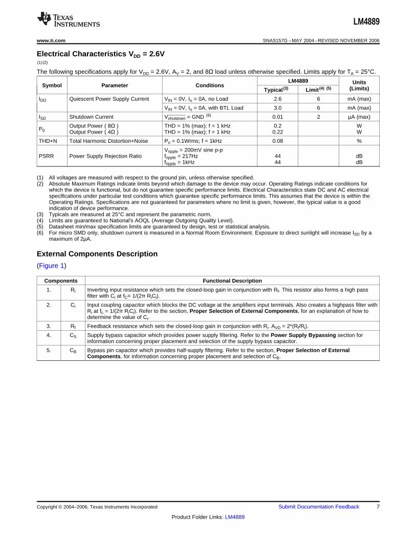
Electrical Characteristics VDD = 2.6V(1) (2)
The following specifications apply for VDD = 2.6V, AV = 2, and 8Ω load unless otherwise specified. Limits apply for TA = 25°C.
LM4889 UnitsSymbol Parameter Conditions (Limits)Typical (3) Limit (4) (5)
IDD Quiescent Power Supply Current VIN = 0V, Io = 0A, no Load 2.6 6 mA (max)
VIN = 0V, Io = 0A, with BTL Load 3.0 6 mA (max)
ISD Shutdown Current Vshutdown = GND (6) 0.01 2 µA (max)
Output Power ( 8Ω ) THD = 1% (max); f = 1 kHz 0.2 WP0 Output Power ( 4Ω ) THD = 1% (max); f = 1 kHz 0.22 W
THD+N Total Harmonic Distortion+Noise Po = 0.1Wrms; f = 1kHz 0.08 %
Vripple = 200mV sine p-pPSRR Power Supply Rejection Ratio fripple = 217Hz 44 dB
fripple = 1kHz 44 dB
(1) All voltages are measured with respect to the ground pin, unless otherwise specified.(2) Absolute Maximum Ratings indicate limits beyond which damage to the device may occur. Operating Ratings indicate conditions for
which the device is functional, but do not guarantee specific performance limits. Electrical Characteristics state DC and AC electricalspecifications under particular test conditions which guarantee specific performance limits. This assumes that the device is within theOperating Ratings. Specifications are not guaranteed for parameters where no limit is given, however, the typical value is a goodindication of device performance.
(3) Typicals are measured at 25°C and represent the parametric norm.(4) Limits are guaranteed to National's AOQL (Average Outgoing Quality Level).(5) Datasheet min/max specification limits are guaranteed by design, test or statistical analysis.(6) For micro SMD only, shutdown current is measured in a Normal Room Environment. Exposure to direct sunlight will increase ISD by a
maximum of 2µA.
External Components Description
(Figure 1)
Components Functional Description
1. Ri Inverting input resistance which sets the closed-loop gain in conjunction with Rf. This resistor also forms a high passfilter with Ci at fC= 1/(2π RiCi).
2. Ci Input coupling capacitor which blocks the DC voltage at the amplifiers input terminals. Also creates a highpass filter withRi at fc = 1/(2π RiCi). Refer to the section, Proper Selection of External Components, for an explanation of how todetermine the value of Ci.
3. Rf Feedback resistance which sets the closed-loop gain in conjunction with Ri. AVD = 2*(Rf/Ri).
4. CS Supply bypass capacitor which provides power supply filtering. Refer to the Power Supply Bypassing section forinformation concerning proper placement and selection of the supply bypass capacitor.
5. CB Bypass pin capacitor which provides half-supply filtering. Refer to the section, Proper Selection of ExternalComponents, for information concerning proper placement and selection of CB.
Copyright © 2004–2006, Texas Instruments Incorporated Submit Documentation Feedback 7
Product Folder Links: LM4889
LM4889
SNAS157G –MAY 2004–REVISED NOVEMBER 2006 www.ti.com
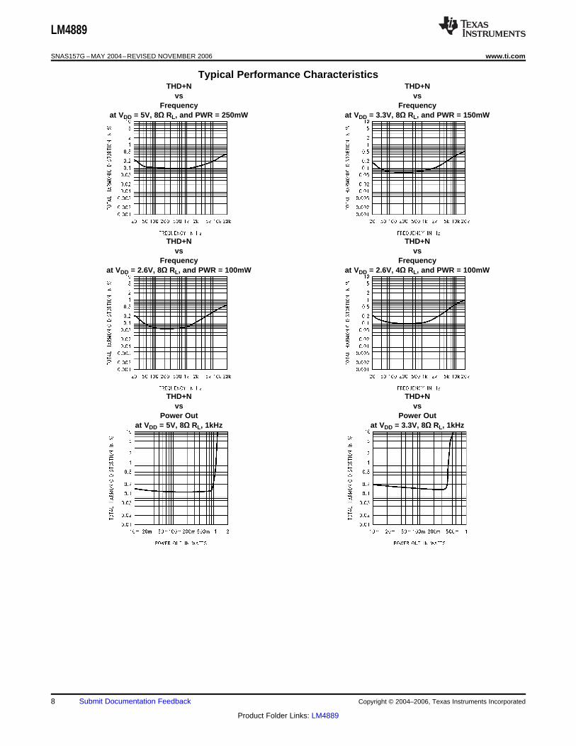
Typical Performance CharacteristicsTHD+N THD+N
vs vsFrequency Frequency
at VDD = 5V, 8Ω RL, and PWR = 250mW at VDD = 3.3V, 8Ω RL, and PWR = 150mW
THD+N THD+Nvs vs
Frequency Frequencyat VDD = 2.6V, 8Ω RL, and PWR = 100mW at VDD = 2.6V, 4Ω RL, and PWR = 100mW
THD+N THD+Nvs vs
Power Out Power Outat VDD = 5V, 8Ω RL, 1kHz at VDD = 3.3V, 8Ω RL, 1kHz
8 Submit Documentation Feedback Copyright © 2004–2006, Texas Instruments Incorporated
Product Folder Links: LM4889
LM4889
www.ti.com SNAS157G –MAY 2004–REVISED NOVEMBER 2006
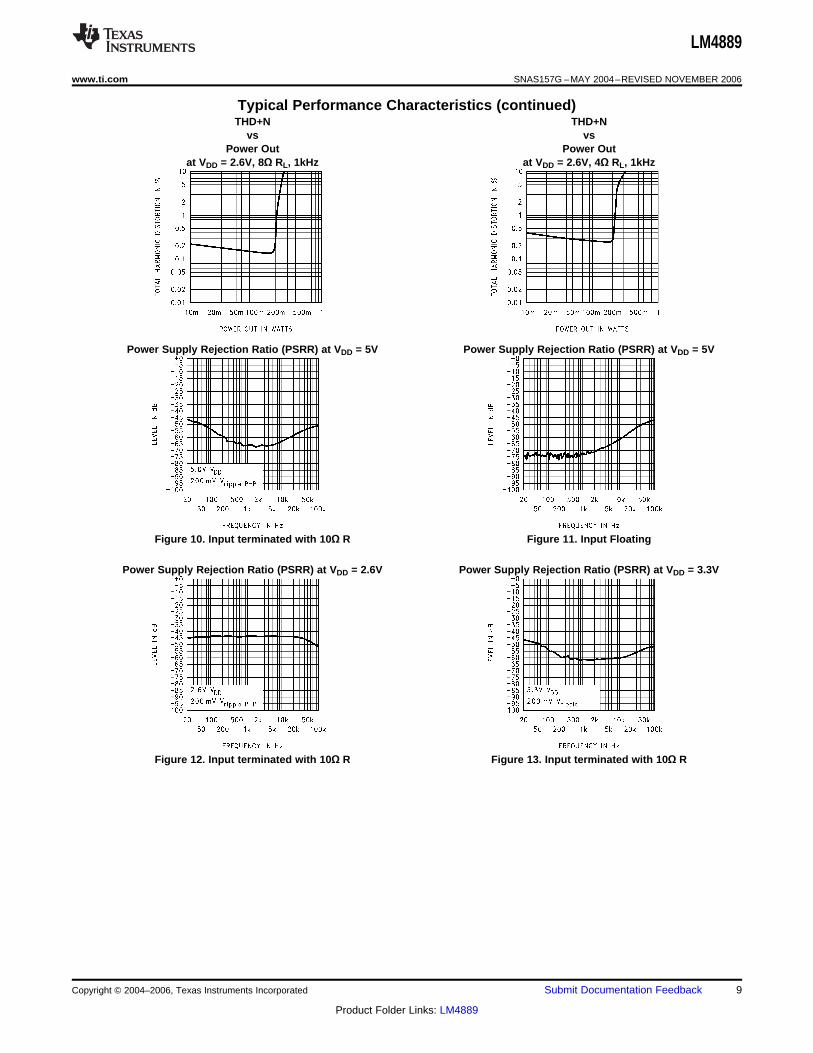
Typical Performance Characteristics (continued)THD+N THD+N
vs vsPower Out Power Out
at VDD = 2.6V, 8Ω RL, 1kHz at VDD = 2.6V, 4Ω RL, 1kHz
Power Supply Rejection Ratio (PSRR) at VDD = 5V Power Supply Rejection Ratio (PSRR) at VDD = 5V
Figure 10. Input terminated with 10Ω R Figure 11. Input Floating
Power Supply Rejection Ratio (PSRR) at VDD = 2.6V Power Supply Rejection Ratio (PSRR) at VDD = 3.3V
Figure 12. Input terminated with 10Ω R Figure 13. Input terminated with 10Ω R
Copyright © 2004–2006, Texas Instruments Incorporated Submit Documentation Feedback 9
Product Folder Links: LM4889
LM4889
SNAS157G –MAY 2004–REVISED NOVEMBER 2006 www.ti.com
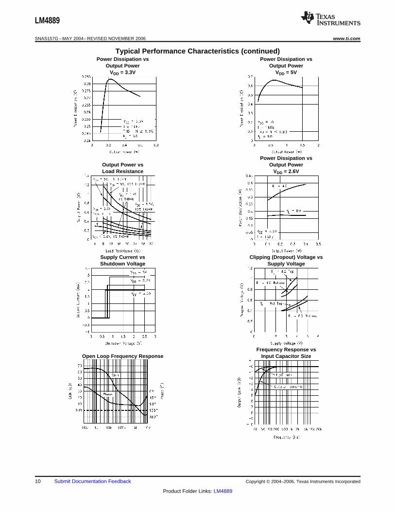
Typical Performance Characteristics (continued)Power Dissipation vs Power Dissipation vs
Output Power Output PowerVDD = 3.3V VDD = 5V
Power Dissipation vsOutput Power vs Output PowerLoad Resistance VDD = 2.6V
Supply Current vs Clipping (Dropout) Voltage vsShutdown Voltage Supply Voltage
Frequency Response vsOpen Loop Frequency Response Input Capacitor Size
10 Submit Documentation Feedback Copyright © 2004–2006, Texas Instruments Incorporated
Product Folder Links: LM4889
LM4889
www.ti.com SNAS157G –MAY 2004–REVISED NOVEMBER 2006
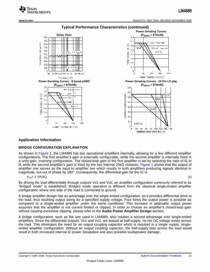
Typical Performance Characteristics (continued)Power Derating Curves
Noise Floor (PDMAX = 670mW)
Power Derating Curves - 8 bump µSMD Power Derating Curves - 10 Pin LD pkg(PDMAX = 670mW) (PDMAX = 670mW)
Application Information
BRIDGE CONFIGURATION EXPLANATION
As shown in Figure 1, the LM4889 has two operational amplifiers internally, allowing for a few different amplifierconfigurations. The first amplifier's gain is externally configurable, while the second amplifier is internally fixed ina unity-gain, inverting configuration. The closed-loop gain of the first amplifier is set by selecting the ratio of Rf toRi while the second amplifier's gain is fixed by the two internal 20kΩ resistors. Figure 1 shows that the output ofamplifier one serves as the input to amplifier two which results in both amplifiers producing signals identical inmagnitude, but out of phase by 180°. Consequently, the differential gain for the IC is
AVD= 2 *(Rf/Ri) (1)
By driving the load differentially through outputs Vo1 and Vo2, an amplifier configuration commonly referred to as“bridged mode” is established. Bridged mode operation is different from the classical single-ended amplifierconfiguration where one side of the load is connected to ground.
A bridge amplifier design has an advantage over the single-ended configuration, as it provides differential drive tothe load, thus doubling output swing for a specified supply voltage. Four times the output power is possible ascompared to a single-ended amplifier under the same conditions. This increase in attainable output powerassumes that the amplifier is not current limited or clipped. In order to choose an amplifier's closed-loop gainwithout causing excessive clipping, please refer to the Audio Power Amplifier Design section.
A bridge configuration, such as the one used in LM4889, also creates a second advantage over single-endedamplifiers. Since the differential outputs, Vo1 and Vo2, are biased at half-supply, no net DC voltage exists acrossthe load. This eliminates the need for an output coupling capacitor which is required in a single supply, single-ended amplifier configuration. Without an output coupling capacitor, the half-supply bias across the load wouldresult in both increased internal IC power dissipation and also possible loudspeaker damage.
Copyright © 2004–2006, Texas Instruments Incorporated Submit Documentation Feedback 11
Product Folder Links: LM4889
LM4889
SNAS157G –MAY 2004–REVISED NOVEMBER 2006 www.ti.com
POWER DISSIPATION
Power dissipation is a major concern when designing a successful amplifier, whether the amplifier is bridged orsingle-ended. A direct consequence of the increased power delivered to the load by a bridge amplifier is anincrease in internal power dissipation. Since the LM4889 has two operational amplifiers in one package, themaximum internal power dissipation is 4 times that of a single-ended amplifier. The maximum power dissipationfor a given application can be derived from the power dissipation graphs or from Equation 1.
PDMAX = 4*(VDD)2/(2π2RL) (1) (2)
It is critical that the maximum junction temperature TJMAX of 150°C is not exceeded. TJMAX can be determinedfrom the power derating curves by using PDMAX and the PC board foil area. By adding additional copper foil, thethermal resistance of the application can be reduced from a free air value of 150°C/W, resulting in higher PDMAX.Additional copper foil can be added to any of the leads connected to the LM4889. It is especially effective whenconnected to VDD, GND, and the output pins. Refer to the application information on the LM4889 reference designboard for an example of good heat sinking. If TJMAX still exceeds 150°C, then additional changes must be made.These changes can include reduced supply voltage, higher load impedance, or reduced ambient temperature.Internal power dissipation is a function of output power. Refer to the Typical Performance Characteristicscurves for power dissipation information for different output powers and output loading.
POWER SUPPLY BYPASSING
As with any amplifier, proper supply bypassing is critical for low noise performance and high power supplyrejection. The capacitor location on both the bypass and power supply pins should be as close to the device aspossible. Typical applications employ a 5V regulator with 10 µF tantalum or electrolytic capacitor and a ceramicbypass capacitor which aid in supply stability. This does not eliminate the need for bypassing the supply nodes ofthe LM4889. The selection of a bypass capacitor, especially CB, is dependent upon PSRR requirements, clickand pop performance (as explained in the section, Proper Selection of External Components), system cost,and size constraints.
SHUTDOWN FUNCTION
In order to reduce power consumption while not in use, the LM4889 contains a shutdown pin to externally turn offthe amplifier's bias circuitry. This shutdown feature turns the amplifier off when a logic low is placed on theshutdown pin. By switching the shutdown pin to ground, the LM4889 supply current draw will be minimized in idlemode. While the device will be disabled with shutdown pin voltages less than 0.5VDC, the idle current may begreater than the typical value of 0.1µA. (Idle current is measured with the shutdown pin grounded).
In many applications, a microcontroller or microprocessor output is used to control the shutdown circuitry toprovide a quick, smooth transition into shutdown. Another solution is to use a single-pole, single-throw switch inconjunction with an external pull-up resistor. When the switch is closed, the shutdown pin is connected to groundand disables the amplifier. If the switch is open, then the external pull-up resistor will enable the LM4889. Thisscheme guarantees that the shutdown pin will not float thus preventing unwanted state changes.
PROPER SELECTION OF EXTERNAL COMPONENTS
Proper selection of external components in applications using integrated power amplifiers is critical to optimizedevice and system performance. While the LM4889 is tolerant of external component combinations,consideration to component values must be used to maximize overall system quality.
The LM4889 is unity-gain stable which gives the designer maximum system flexibility. The LM4889 should beused in low gain configurations to minimize THD+N values, and maximize the signal to noise ratio. Low gainconfigurations require large input signals to obtain a given output power. Input signals equal to or greater than 1Vrms are available from sources such as audio codecs. Please refer to the section, Audio Power AmplifierDesign, for a more complete explanation of proper gain selection.
Besides gain, one of the major considerations is the closed-loop bandwidth of the amplifier. To a large extent, thebandwidth is dictated by the choice of external components shown in Figure 1. The input coupling capacitor, Ci,forms a first order high pass filter which limits low frequency response. This value should be chosen based onneeded frequency response for a few reasons.
12 Submit Documentation Feedback Copyright © 2004–2006, Texas Instruments Incorporated
Product Folder Links: LM4889
LM4889
www.ti.com SNAS157G –MAY 2004–REVISED NOVEMBER 2006
SELECTION OF INPUT CAPACITOR SIZE
Large input capacitors are both expensive and space hungry for portable designs. Clearly, a certain sizedcapacitor is needed to couple in low frequencies without severe attenuation. But in many cases the speakersused in portable systems, whether internal or external, have little ability to reproduce signals below 100 Hz to150 Hz. Thus, using a large input capacitor may not increase actual system performance.
In addition to system cost and size, click and pop performance is effected by the size of the input couplingcapacitor, Ci. A larger input coupling capacitor requires more charge to reach its quiescent DC voltage (nominally1/2 VDD). This charge comes from the output via the feedback and is apt to create pops upon device enable.Thus, by minimizing the capacitor size based on necessary low frequency response, turn-on pops can beminimized.
Besides minimizing the input capacitor size, careful consideration should be paid to the bypass capacitor value.Bypass capacitor, CB, is the most critical component to minimize turn-on pops since it determines how fast theLM4889 turns on. The slower the LM4889's outputs ramp to their quiescent DC voltage (nominally 1/2 VDD), thesmaller the turn-on pop. Choosing CB equal to 1.0 µF along with a small value of Ci (in the range of 0.1 µF to0.39 µF), should produce a virtually clickless and popless shutdown function. While the device will functionproperly, (no oscillations or motorboating), with CB equal to 0.1 µF, the device will be much more susceptible toturn-on clicks and pops. Thus, a value of CB equal to 1.0 µF is recommended in all but the most cost sensitivedesigns.
AUDIO POWER AMPLIFIER DESIGN
A 1W/8Ω Audio Amplifier
Given:
Power Output 1 Wrms
Load Impedance 8ΩInput Level 1 Vrms
Input Impedance 20 kΩBandwidth 100 Hz–20 kHz ± 0.25 dB
A designer must first determine the minimum supply rail to obtain the specified output power. By extrapolatingfrom the Output Power vs Supply Voltage graphs in the Typical Performance Characteristics section, thesupply rail can be easily found. A second way to determine the minimum supply rail is to calculate the requiredVopeak using Equation 2 and add the output voltage. Using this method, the minimum supply voltage would be(Vopeak + (VODTOP + VODBOT)), where VODBOT and VODTOP are extrapolated from the Dropout Voltage vs SupplyVoltage curve in the Typical Performance Characteristics section.
(2) (3)
5V is a standard voltage in most applications, it is chosen for the supply rail. Extra supply voltage createsheadroom that allows the LM4889 to reproduce peaks in excess of 1W without producing audible distortion. Atthis time, the designer must make sure that the power supply choice along with the output impedance does notviolate the conditions explained in the Power Dissipation section.
Once the power dissipation equations have been addressed, the required differential gain can be determinedfrom Equation 3.
(3) (4)
Rf/Ri = AVD/2 (5)
From Equation 3, the minimum AVD is 2.83; use AVD = 3.
Copyright © 2004–2006, Texas Instruments Incorporated Submit Documentation Feedback 13
Product Folder Links: LM4889
LM4889
SNAS157G –MAY 2004–REVISED NOVEMBER 2006 www.ti.com
Since the desired input impedance was 20 kΩ, and with a AVD impedance of 2, a ratio of 1.5:1 of Rf to Ri resultsin an allocation of Ri = 20 kΩ and Rf = 30 kΩ. The final design step is to address the bandwidth requirementswhich must be stated as a pair of −3 dB frequency points. Five times away from a −3 dB point is 0.17 dB downfrom passband response which is better than the required ±0.25 dB specified.
fL = 100 Hz/5 = 20 Hz
fH = 20 kHz * 5 = 100 kHz
As stated in the External Components section, Ri in conjunction with Ci create a highpass filter.
Ci ≥ 1/(2π*20 kΩ*20 Hz) = 0.397 µF; use 0.39 µF
The high frequency pole is determined by the product of the desired frequency pole, fH, and the differential gain,AVD. With a AVD = 3 and fH = 100 kHz, the resulting GBWP = 300kHz which is much smaller than the LM4889GBWP of 2.5MHz. This calculation shows that if a designer has a need to design an amplifier with a higherdifferential gain, the LM4889 can still be used without running into bandwidth limitations.
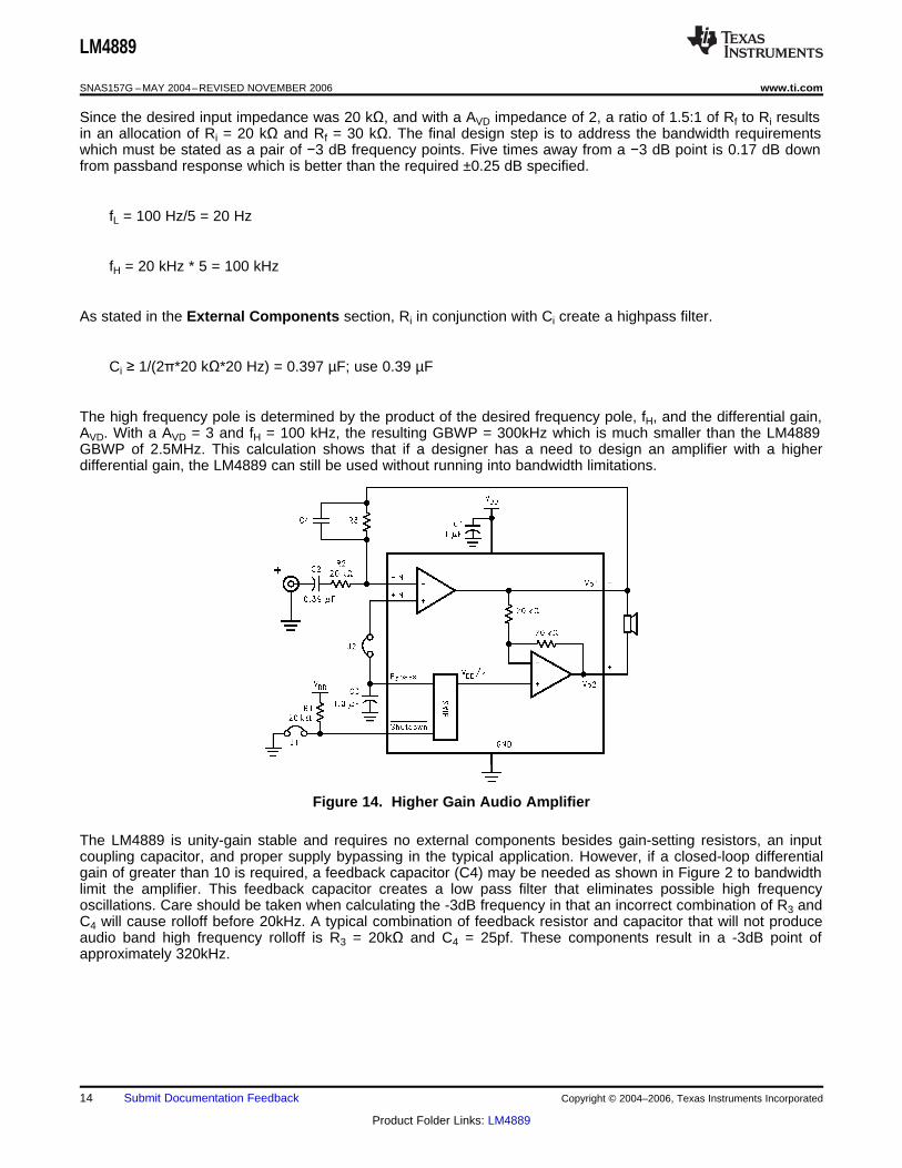
Figure 14. Higher Gain Audio Amplifier
The LM4889 is unity-gain stable and requires no external components besides gain-setting resistors, an inputcoupling capacitor, and proper supply bypassing in the typical application. However, if a closed-loop differentialgain of greater than 10 is required, a feedback capacitor (C4) may be needed as shown in Figure 2 to bandwidthlimit the amplifier. This feedback capacitor creates a low pass filter that eliminates possible high frequencyoscillations. Care should be taken when calculating the -3dB frequency in that an incorrect combination of R3 andC4 will cause rolloff before 20kHz. A typical combination of feedback resistor and capacitor that will not produceaudio band high frequency rolloff is R3 = 20kΩ and C4 = 25pf. These components result in a -3dB point ofapproximately 320kHz.
14 Submit Documentation Feedback Copyright © 2004–2006, Texas Instruments Incorporated
Product Folder Links: LM4889
LM4889
www.ti.com SNAS157G –MAY 2004–REVISED NOVEMBER 2006
Figure 15. Differential Amplifier Configuration for LM4889
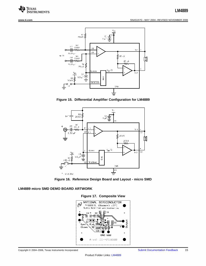
Figure 16. Reference Design Board and Layout - micro SMD
LM4889 micro SMD DEMO BOARD ARTWORK
Figure 17. Composite View
Copyright © 2004–2006, Texas Instruments Incorporated Submit Documentation Feedback 15
Product Folder Links: LM4889
LM4889
SNAS157G –MAY 2004–REVISED NOVEMBER 2006 www.ti.com
Figure 18. Silk Screen
Figure 19. Top Layer
Figure 20. Bottom Layer
16 Submit Documentation Feedback Copyright © 2004–2006, Texas Instruments Incorporated
Product Folder Links: LM4889
LM4889
www.ti.com SNAS157G –MAY 2004–REVISED NOVEMBER 2006
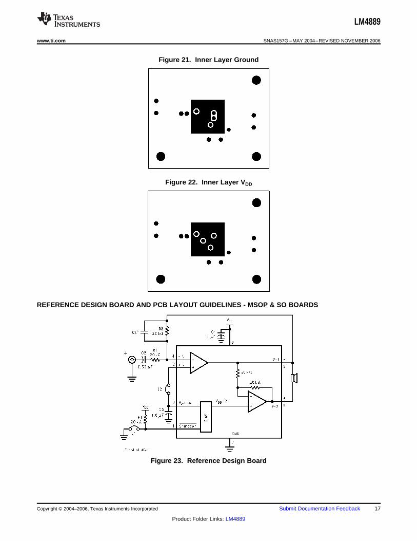
Figure 21. Inner Layer Ground
Figure 22. Inner Layer VDD
REFERENCE DESIGN BOARD AND PCB LAYOUT GUIDELINES - MSOP & SO BOARDS
Figure 23. Reference Design Board
Copyright © 2004–2006, Texas Instruments Incorporated Submit Documentation Feedback 17
Product Folder Links: LM4889
LM4889
SNAS157G –MAY 2004–REVISED NOVEMBER 2006 www.ti.com
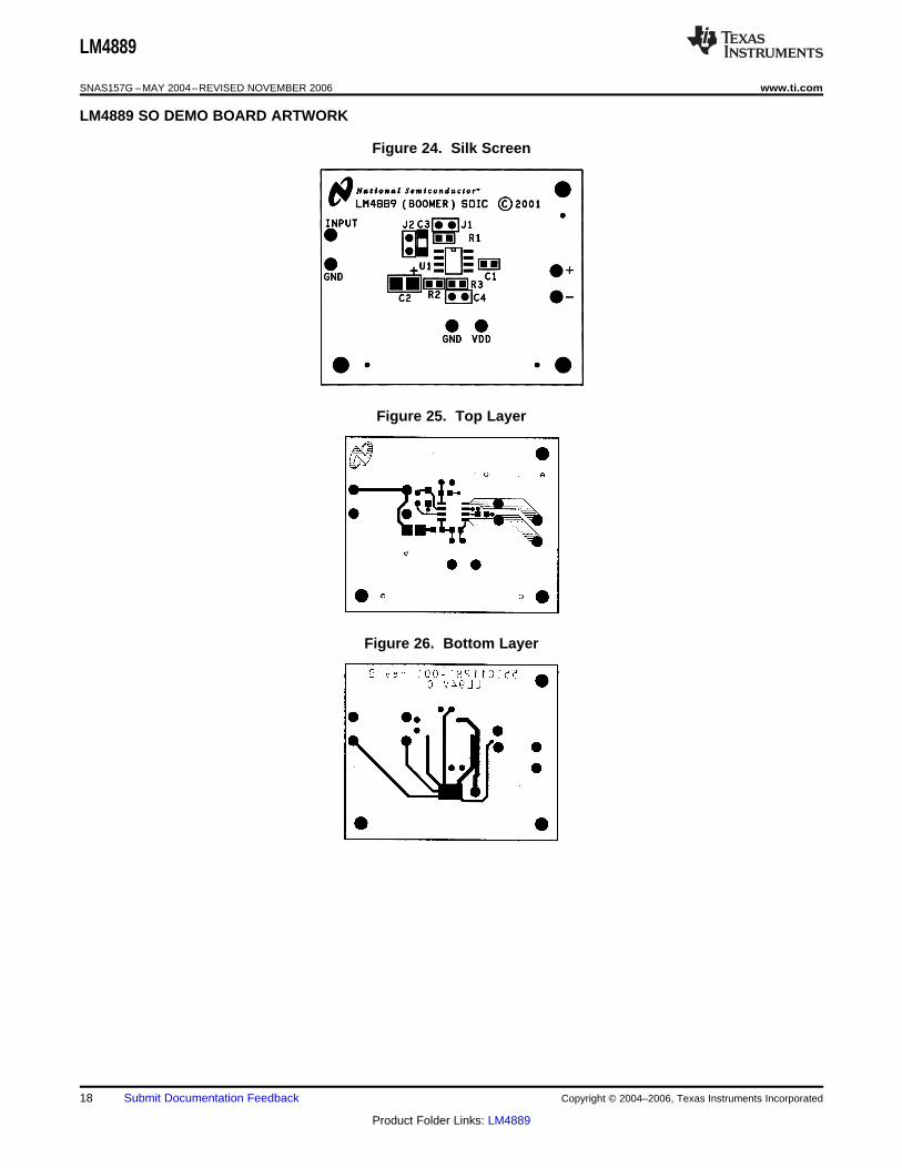
LM4889 SO DEMO BOARD ARTWORK
Figure 24. Silk Screen
Figure 25. Top Layer
Figure 26. Bottom Layer
18 Submit Documentation Feedback Copyright © 2004–2006, Texas Instruments Incorporated
Product Folder Links: LM4889
LM4889
www.ti.com SNAS157G –MAY 2004–REVISED NOVEMBER 2006
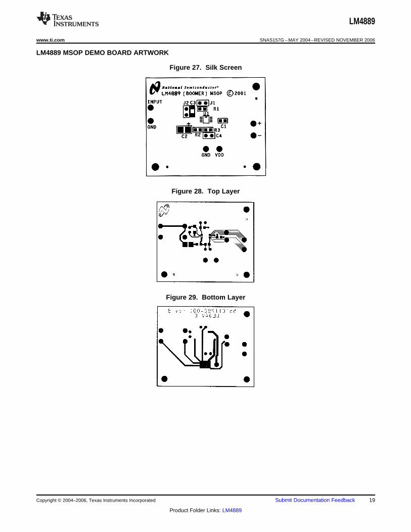
LM4889 MSOP DEMO BOARD ARTWORK
Figure 27. Silk Screen
Figure 28. Top Layer
Figure 29. Bottom Layer
Copyright © 2004–2006, Texas Instruments Incorporated Submit Documentation Feedback 19
Product Folder Links: LM4889
PACKAGE OPTION ADDENDUM
www.ti.com 17-Nov-2012
Addendum-Page 1
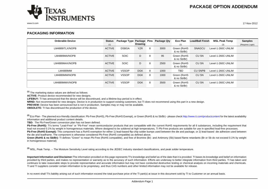
PACKAGING INFORMATION
Orderable Device Status(1)
Package Type PackageDrawing
Pins Package Qty Eco Plan(2)
Lead/Ball Finish MSL Peak Temp(3)
Samples(Requires Login)
LM4889ITLX/NOPB ACTIVE DSBGA YZR 8 3000 Green (RoHS& no Sb/Br)
SNAGCU Level-1-260C-UNLIM
LM4889MA/NOPB ACTIVE SOIC D 8 95 Green (RoHS& no Sb/Br)
CU SN Level-1-260C-UNLIM
LM4889MAX/NOPB ACTIVE SOIC D 8 2500 Green (RoHS& no Sb/Br)
CU SN Level-1-260C-UNLIM
LM4889MM ACTIVE VSSOP DGK 8 1000 TBD CU SNPB Level-1-260C-UNLIM
LM4889MM/NOPB ACTIVE VSSOP DGK 8 1000 Green (RoHS& no Sb/Br)
CU SN Level-1-260C-UNLIM
LM4889MMX/NOPB ACTIVE VSSOP DGK 8 3500 Green (RoHS& no Sb/Br)
CU SN Level-1-260C-UNLIM
(1) The marketing status values are defined as follows:ACTIVE: Product device recommended for new designs.LIFEBUY: TI has announced that the device will be discontinued, and a lifetime-buy period is in effect.NRND: Not recommended for new designs. Device is in production to support existing customers, but TI does not recommend using this part in a new design.PREVIEW: Device has been announced but is not in production. Samples may or may not be available.OBSOLETE: TI has discontinued the production of the device.
(2) Eco Plan - The planned eco-friendly classification: Pb-Free (RoHS), Pb-Free (RoHS Exempt), or Green (RoHS & no Sb/Br) - please check http://www.ti.com/productcontent for the latest availabilityinformation and additional product content details.TBD: The Pb-Free/Green conversion plan has not been defined.Pb-Free (RoHS): TI's terms "Lead-Free" or "Pb-Free" mean semiconductor products that are compatible with the current RoHS requirements for all 6 substances, including the requirement thatlead not exceed 0.1% by weight in homogeneous materials. Where designed to be soldered at high temperatures, TI Pb-Free products are suitable for use in specified lead-free processes.Pb-Free (RoHS Exempt): This component has a RoHS exemption for either 1) lead-based flip-chip solder bumps used between the die and package, or 2) lead-based die adhesive used betweenthe die and leadframe. The component is otherwise considered Pb-Free (RoHS compatible) as defined above.Green (RoHS & no Sb/Br): TI defines "Green" to mean Pb-Free (RoHS compatible), and free of Bromine (Br) and Antimony (Sb) based flame retardants (Br or Sb do not exceed 0.1% by weightin homogeneous material)
(3) MSL, Peak Temp. -- The Moisture Sensitivity Level rating according to the JEDEC industry standard classifications, and peak solder temperature.
Important Information and Disclaimer:The information provided on this page represents TI's knowledge and belief as of the date that it is provided. TI bases its knowledge and belief on informationprovided by third parties, and makes no representation or warranty as to the accuracy of such information. Efforts are underway to better integrate information from third parties. TI has taken andcontinues to take reasonable steps to provide representative and accurate information but may not have conducted destructive testing or chemical analysis on incoming materials and chemicals.TI and TI suppliers consider certain information to be proprietary, and thus CAS numbers and other limited information may not be available for release.
In no event shall TI's liability arising out of such information exceed the total purchase price of the TI part(s) at issue in this document sold by TI to Customer on an annual basis.
PACKAGE OPTION ADDENDUM
www.ti.com 17-Nov-2012
Addendum-Page 2
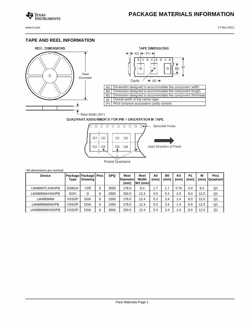
TAPE AND REEL INFORMATION
*All dimensions are nominal
Device PackageType
PackageDrawing
Pins SPQ ReelDiameter
(mm)
ReelWidth
W1 (mm)
A0(mm)
B0(mm)
K0(mm)
P1(mm)
W(mm)
Pin1Quadrant
LM4889ITLX/NOPB DSBGA YZR 8 3000 178.0 8.4 1.7 1.7 0.76 4.0 8.0 Q1
LM4889MAX/NOPB SOIC D 8 2500 330.0 12.4 6.5 5.4 2.0 8.0 12.0 Q1
LM4889MM VSSOP DGK 8 1000 178.0 12.4 5.3 3.4 1.4 8.0 12.0 Q1
LM4889MM/NOPB VSSOP DGK 8 1000 178.0 12.4 5.3 3.4 1.4 8.0 12.0 Q1
LM4889MMX/NOPB VSSOP DGK 8 3500 330.0 12.4 5.3 3.4 1.4 8.0 12.0 Q1
PACKAGE MATERIALS INFORMATION
www.ti.com 17-Nov-2012
Pack Materials-Page 1
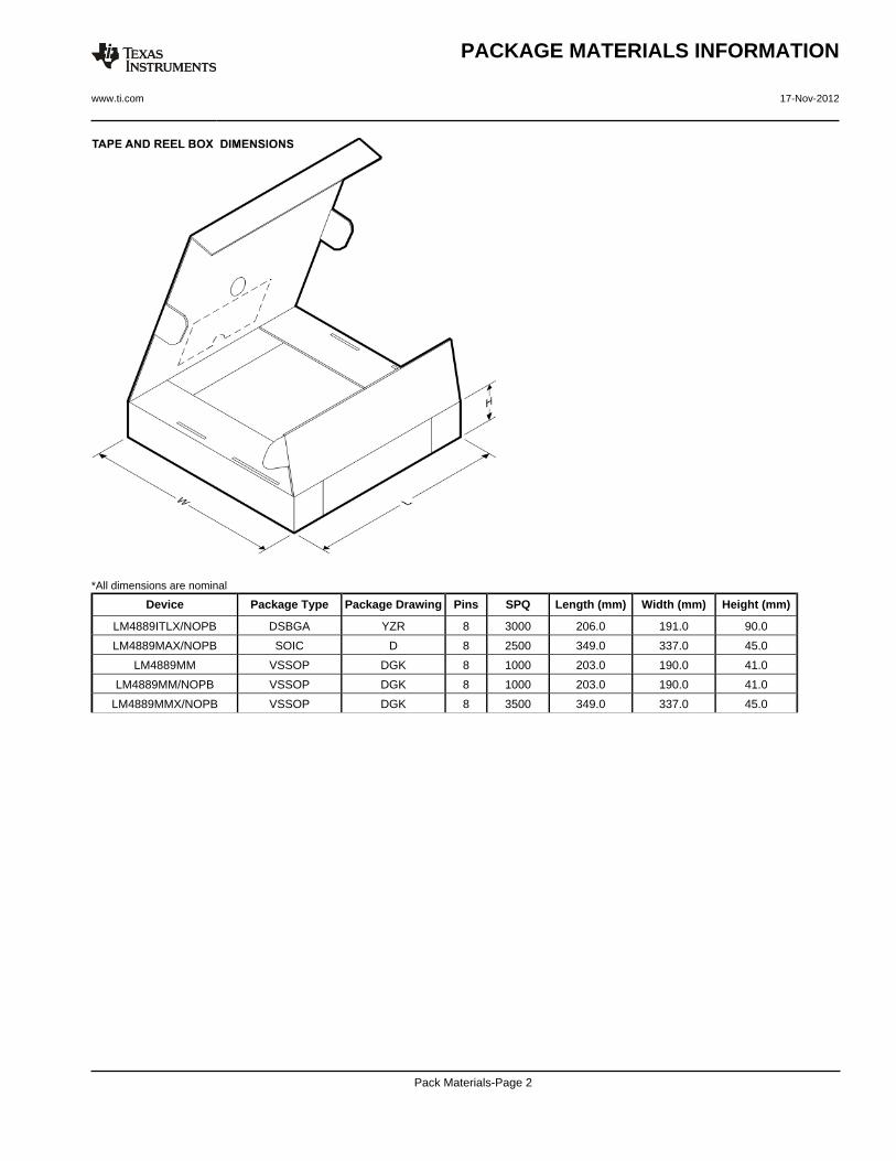
*All dimensions are nominal
Device Package Type Package Drawing Pins SPQ Length (mm) Width (mm) Height (mm)
LM4889ITLX/NOPB DSBGA YZR 8 3000 206.0 191.0 90.0
LM4889MAX/NOPB SOIC D 8 2500 349.0 337.0 45.0
LM4889MM VSSOP DGK 8 1000 203.0 190.0 41.0
LM4889MM/NOPB VSSOP DGK 8 1000 203.0 190.0 41.0
LM4889MMX/NOPB VSSOP DGK 8 3500 349.0 337.0 45.0
PACKAGE MATERIALS INFORMATION
www.ti.com 17-Nov-2012
Pack Materials-Page 2
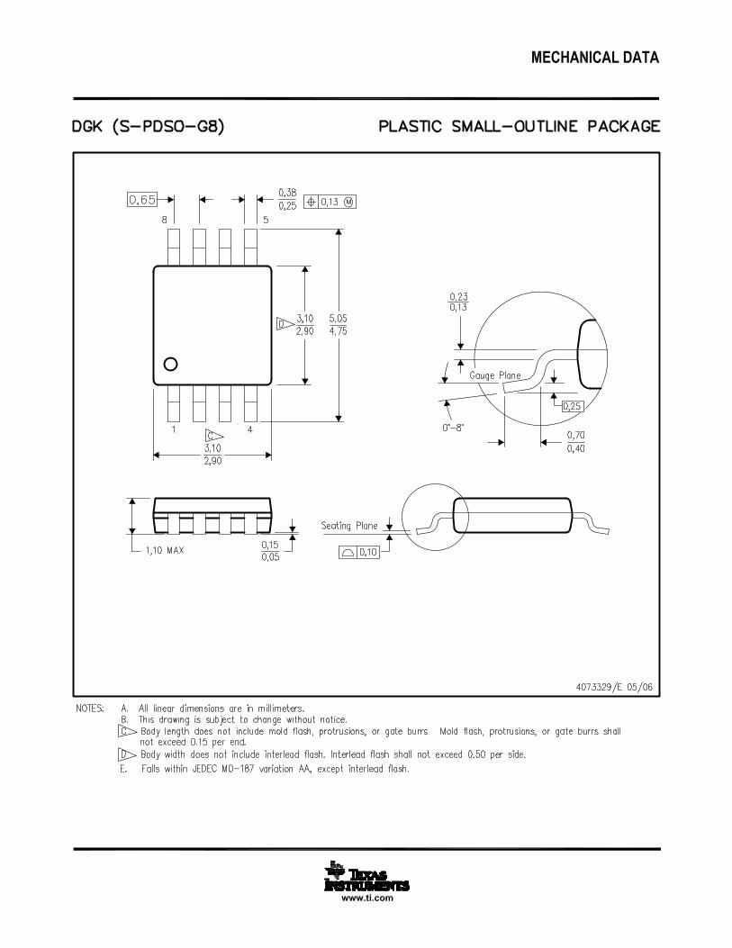
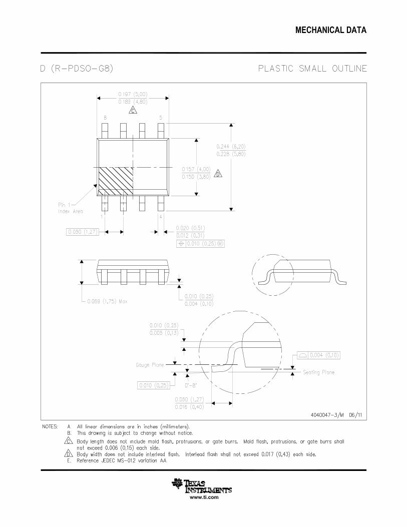
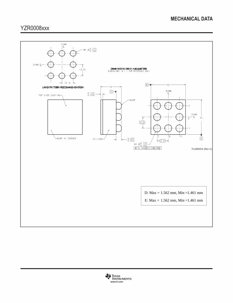
MECHANICAL DATA
YZR0008xxx
www.ti.com
TLA08XXX (Rev C)
D: Max =
E: Max =
1.562 mm, Min =
1.562 mm, Min =
1.461 mm
1.461 mm
IMPORTANT NOTICE
Texas Instruments Incorporated and its subsidiaries (TI) reserve the right to make corrections, enhancements, improvements and otherchanges to its semiconductor products and services per JESD46, latest issue, and to discontinue any product or service per JESD48, latestissue. Buyers should obtain the latest relevant information before placing orders and should verify that such information is current andcomplete. All semiconductor products (also referred to herein as “components”) are sold subject to TI’s terms and conditions of salesupplied at the time of order acknowledgment.
TI warrants performance of its components to the specifications applicable at the time of sale, in accordance with the warranty in TI’s termsand conditions of sale of semiconductor products. Testing and other quality control techniques are used to the extent TI deems necessaryto support this warranty. Except where mandated by applicable law, testing of all parameters of each component is not necessarilyperformed.
TI assumes no liability for applications assistance or the design of Buyers’ products. Buyers are responsible for their products andapplications using TI components. To minimize the risks associated with Buyers’ products and applications, Buyers should provideadequate design and operating safeguards.
TI does not warrant or represent that any license, either express or implied, is granted under any patent right, copyright, mask work right, orother intellectual property right relating to any combination, machine, or process in which TI components or services are used. Informationpublished by TI regarding third-party products or services does not constitute a license to use such products or services or a warranty orendorsement thereof. Use of such information may require a license from a third party under the patents or other intellectual property of thethird party, or a license from TI under the patents or other intellectual property of TI.
Reproduction of significant portions of TI information in TI data books or data sheets is permissible only if reproduction is without alterationand is accompanied by all associated warranties, conditions, limitations, and notices. TI is not responsible or liable for such altereddocumentation. Information of third parties may be subject to additional restrictions.
Resale of TI components or services with statements different from or beyond the parameters stated by TI for that component or servicevoids all express and any implied warranties for the associated TI component or service and is an unfair and deceptive business practice.TI is not responsible or liable for any such statements.
Buyer acknowledges and agrees that it is solely responsible for compliance with all legal, regulatory and safety-related requirementsconcerning its products, and any use of TI components in its applications, notwithstanding any applications-related information or supportthat may be provided by TI. Buyer represents and agrees that it has all the necessary expertise to create and implement safeguards whichanticipate dangerous consequences of failures, monitor failures and their consequences, lessen the likelihood of failures that might causeharm and take appropriate remedial actions. Buyer will fully indemnify TI and its representatives against any damages arising out of the useof any TI components in safety-critical applications.
In some cases, TI components may be promoted specifically to facilitate safety-related applications. With such components, TI’s goal is tohelp enable customers to design and create their own end-product solutions that meet applicable functional safety standards andrequirements. Nonetheless, such components are subject to these terms.
No TI components are authorized for use in FDA Class III (or similar life-critical medical equipment) unless authorized officers of the partieshave executed a special agreement specifically governing such use.
Only those TI components which TI has specifically designated as military grade or “enhanced plastic” are designed and intended for use inmilitary/aerospace applications or environments. Buyer acknowledges and agrees that any military or aerospace use of TI componentswhich have not been so designated is solely at the Buyer's risk, and that Buyer is solely responsible for compliance with all legal andregulatory requirements in connection with such use.
TI has specifically designated certain components as meeting ISO/TS16949 requirements, mainly for automotive use. In any case of use ofnon-designated products, TI will not be responsible for any failure to meet ISO/TS16949.
Products Applications
Audio www.ti.com/audio Automotive and Transportation www.ti.com/automotive
Amplifiers amplifier.ti.com Communications and Telecom www.ti.com/communications
Data Converters dataconverter.ti.com Computers and Peripherals www.ti.com/computers
DLP® Products www.dlp.com Consumer Electronics www.ti.com/consumer-apps
DSP dsp.ti.com Energy and Lighting www.ti.com/energy
Clocks and Timers www.ti.com/clocks Industrial www.ti.com/industrial
Interface interface.ti.com Medical www.ti.com/medical
Logic logic.ti.com Security www.ti.com/security
Power Mgmt power.ti.com Space, Avionics and Defense www.ti.com/space-avionics-defense
Microcontrollers microcontroller.ti.com Video and Imaging www.ti.com/video
RFID www.ti-rfid.com
OMAP Applications Processors www.ti.com/omap TI E2E Community e2e.ti.com
Wireless Connectivity www.ti.com/wirelessconnectivity
Mailing Address: Texas Instruments, Post Office Box 655303, Dallas, Texas 75265Copyright © 2012, Texas Instruments Incorporated
Mouser Electronics
Authorized Distributor
Click to View Pricing, Inventory, Delivery & Lifecycle Information: Texas Instruments:
LM4889ITLX/NOPB LM4889MA LM4889MAX LM4889MMX