LM311 IC Data sheet
10
1/9 s MAXIMUM INPUT CURRENT : 150nA s MAXIMUM OFFSET CURRENT : 20nA s DIFFERENTIAL INPUT VOLT AGE RANGE : ±30V s POWER CONSUMPTION :135mW AT ±15V s SUPPLY VOLTAGE : +5V TO ±15V s OUTPUT CURRENT : 50mA DESCRIPTION The LM111, LM211, LM311 are voltage compara- tors that have low input currents. They are also designed to operate over a wide range of supply voltages : from standard ±15V op- erational amplifier supplies down to the single +5V supply used for IC logic. Their output is compatible with RTL-DTL and TTL as well as MOS circuits and can switch voltages up to +50V at outputs currents as high as 50mA. ORDER CODE N = Dual in Line Package (DIP) D = Small Outline Package (SO) - also available in Tape & Reel (DT) PIN CONNECTIONS (top view) Part Number Temperature Range Package N D LM111 -55 ° C, +125 ° C • • LM211 -4 0° C, +105° C • • LM311 0° C, +70° C • • Example : LM311D D SO8 N DIP8 1 2 3 4 8 7 6 5 1 - Ground 2 - Non-inverting input 3 - Inverting input 4 - V CC - 5 - Balance 6 - Strobe/Balance 7 - Output 8 - V CC + LM111 LM211 - LM311 VOLTAGE COMPARATORS June 2002
Transcript of LM311 IC Data sheet

8/7/2019 LM311 IC Data sheet
http://slidepdf.com/reader/full/lm311-ic-data-sheet 1/10
1/9
s MAXIMUM INPUT CURRENT : 150nA
s MAXIMUM OFFSET CURRENT : 20nA
s DIFFERENTIAL INPUT VOLTAGE RANGE :
±30V
s POWER CONSUMPTION :135mW AT ±15V
s SUPPLY VOLTAGE : +5V TO ±15V
s OUTPUT CURRENT : 50mA
DESCRIPTION
The LM111, LM211, LM311 are voltage compara-
tors that have low input currents.
They are also designed to operate over a wide
range of supply voltages : from standard ±15V op-
erational amplifier supplies down to the single +5V
supply used for IC logic.
Their output is compatible with RTL-DTL and TTL
as well as MOS circuits and can switch voltages
up to +50V at outputs currents as high as 50mA.
ORDER CODE
N = Dual in Line Package (DIP)
D = Small Outline Package (SO) - also available in Tape & Reel (DT)
PIN CONNECTIONS (top view)
Part NumberTemperature
Range
Package
N D
LM111 -55°C, +125°C • •
LM211 -40°C, +105°C • •
LM311 0°C, +70°C • •
Example : LM311D
DSO8
NDIP8
1
2
3
4
8
7
6
5
1 - Ground2 - Non-inverting input3 - Inverting input
4 - VCC-
5 - Balance6 - Strobe/Balance
7 - Output
8 - VCC+
LM111LM211 - LM311
VOLTAGE COMPARATORS
June 2002
8/7/2019 LM311 IC Data sheet
http://slidepdf.com/reader/full/lm311-ic-data-sheet 2/10
LM111-LM211-LM311
2/9
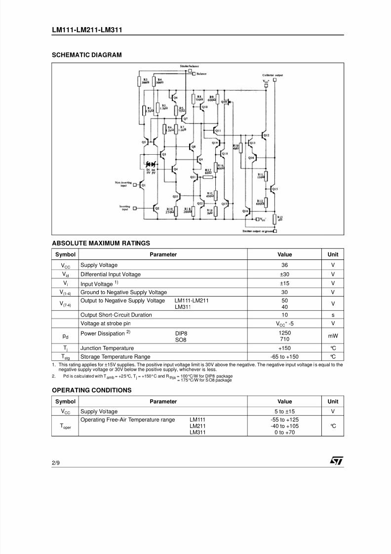
SCHEMATIC DIAGRAM
ABSOLUTE MAXIMUM RATINGS
OPERATING CONDITIONS
Symbol Parameter Value Unit
VCC Supply Voltage 36 V
Vid Differential Input Voltage ±30 V
Vi Input Voltage 1)
1. This rating applies for ±15V supplies. The positive input voltage limit is 30V above the negative. The negative input voltage is equal to thenegative supply voltage or 30V below the positive supply, whichever is less.
±15 V
V(1-4) Ground to Negative Supply Voltage 30 V
V(7-4)Output to Negative Supply Voltage LM111-LM211
LM3115040
V
Output Short-Circuit Duration 10 s
Voltage at strobe pin VCC+ -5 V
pdPower Dissipation 2) DIP8
SO8
2. Pd is calculated with Tamb = +25°C, T j = +150°C and R thja = 100°C/W for DIP8 package= 175°C/W for SO8 package
1250710
mW
Tj Junction Temperature +150 °C
Tstg Storage Temperature Range -65 to +150 °C
Symbol Parameter Value Unit
VCC Supply Voltage 5 to ±15 V
Toper
Operating Free-Air Temperature range LM111LM211LM311
-55 to +125-40 to +105
0 to +70°C
8/7/2019 LM311 IC Data sheet
http://slidepdf.com/reader/full/lm311-ic-data-sheet 3/10
LM111-LM211-LM311
3/9
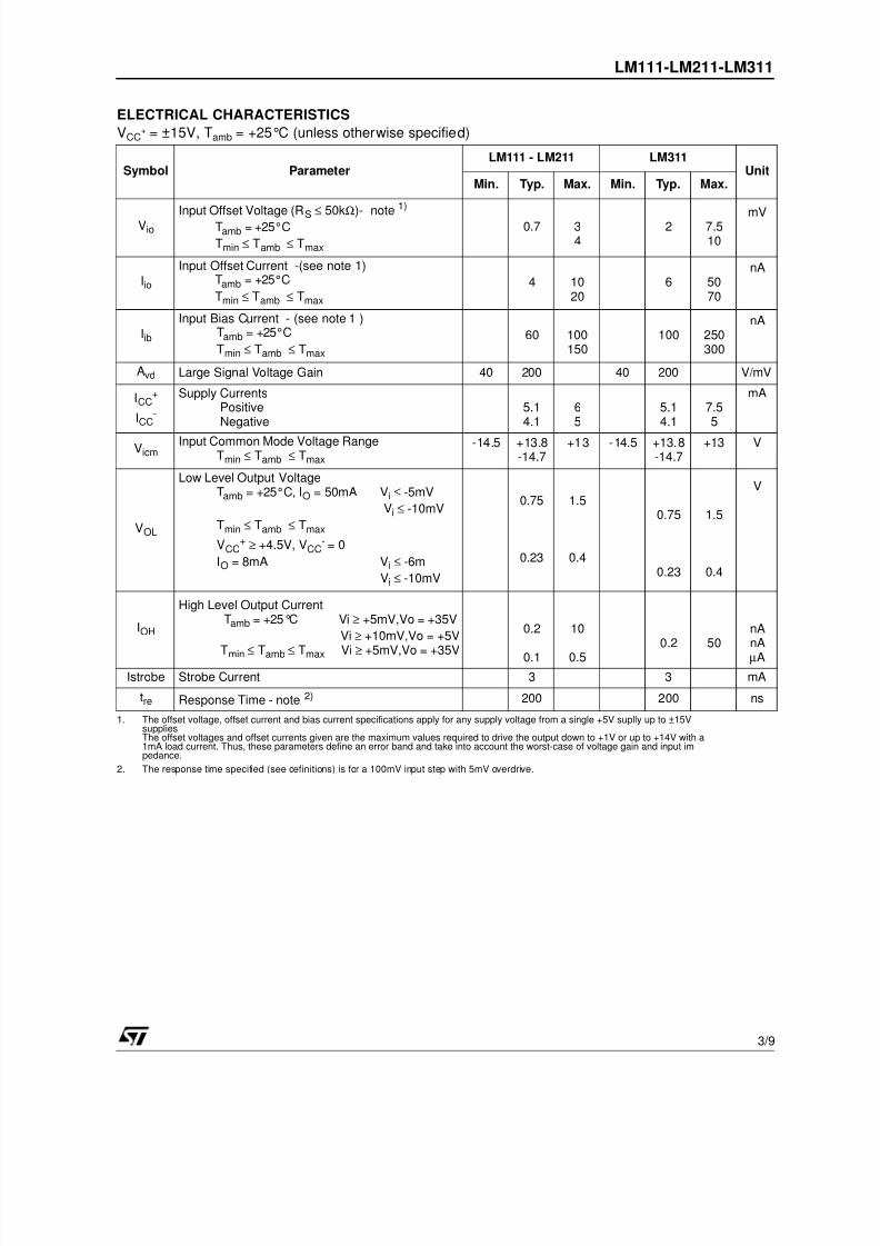
ELECTRICAL CHARACTERISTICS
VCC+ = ±15V, Tamb = +25°C (unless otherwise specified)
Symbol ParameterLM111 - LM211 LM311
UnitMin. Typ. Max. Min. Typ. Max.
Vio
Input Offset Voltage (RS ≤ 50kΩ)- note 1)
Tamb = +25°C
Tmin ≤ Tamb ≤ Tmax
1. The offset voltage, offset current and bias current specifications apply for any supply voltage from a single +5V suplly up to ±15VsuppliesThe offset voltages and offset currents given are the maximum values required to drive the output down to +1V or up to +14V with a1mA load current. Thus, these parameters define an error band and take into account the worst-case of voltage gain and input impedance.
0.7 34
2 7.510
mV
Iio
Input Offset Current -(see note 1)Tamb = +25°C
Tmin ≤ Tamb ≤ Tmax
4 1020
6 5070
nA
Iib
Input Bias Current - (see note 1 )Tamb = +25°C
Tmin ≤ Tamb ≤ Tmax
60 100150
100 250300
nA
Avd Large Signal Voltage Gain 40 200 40 200 V/mV
ICC+
ICC-
Supply CurrentsPositiveNegative
5.14.1
65
5.14.1
7.55
mA
VicmInput Common Mode Voltage Range
Tmin ≤ Tamb ≤ Tmax
-14.5 +13.8-14.7
+13 -14.5 +13.8-14.7
+13 V
VOL
Low Level Output VoltageTamb = +25°C, IO = 50mA Vi ≤ -5mV
Vi ≤ -10mV
Tmin ≤ Tamb ≤ Tmax
VCC+ ≥ +4.5V, VCC
- = 0
IO = 8mA Vi ≤ -6m
Vi ≤ -10mV
0.75
0.23
1.5
0.4
0.75
0.23
1.5
0.4
V
IOH
High Level Output CurrentTamb = +25°C Vi ≥ +5mV,Vo = +35V
Vi ≥ +10mV,Vo = +5V
Tmin ≤ Tamb ≤ Tmax Vi ≥ +5mV,Vo = +35V
0.2
0.1
10
0.5
0.2 50nAnA
µA
Istrobe Strobe Current 3 3 mA
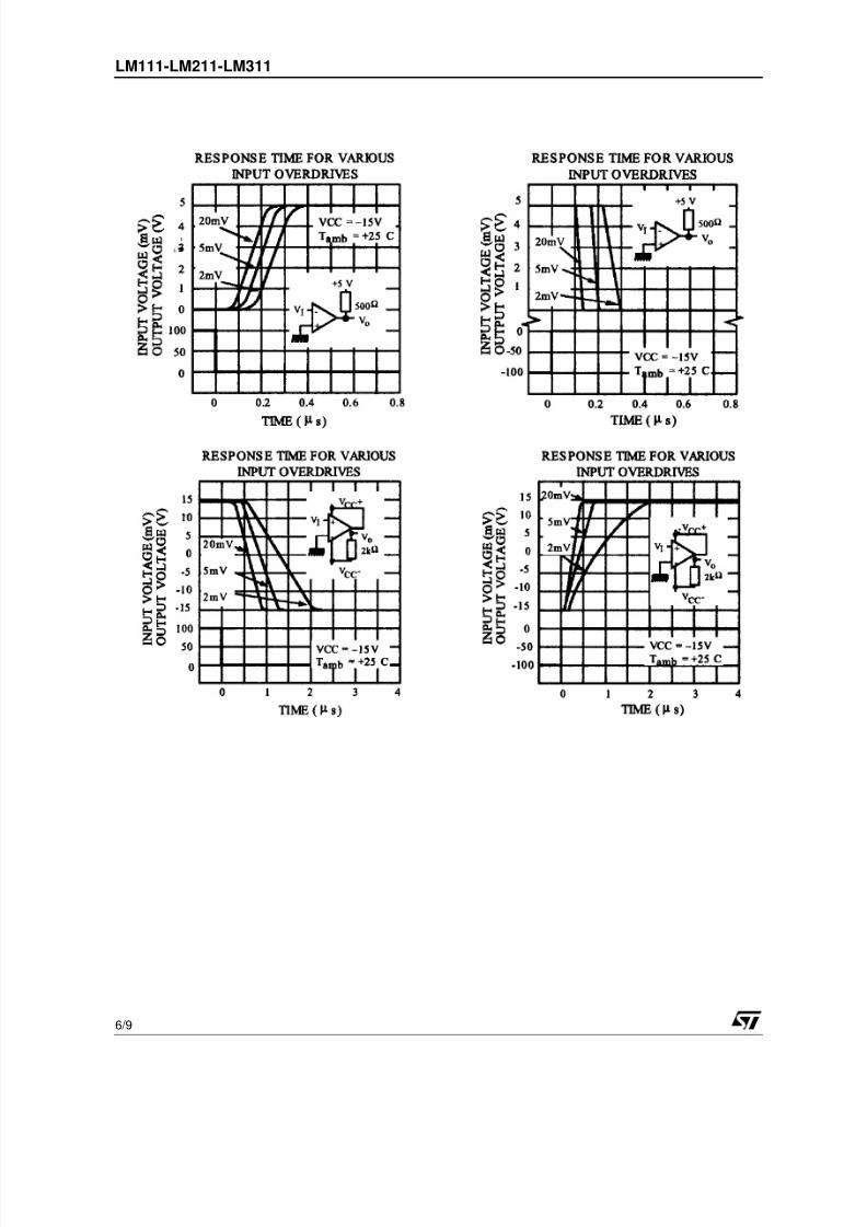
tre Response Time - note 2)
2. The response time specified (see definitions) is for a 100mV input step with 5mV overdrive.
200 200 ns

8/7/2019 LM311 IC Data sheet
http://slidepdf.com/reader/full/lm311-ic-data-sheet 4/10
LM111-LM211-LM311
4/9
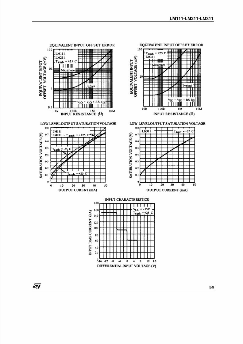
8/7/2019 LM311 IC Data sheet
http://slidepdf.com/reader/full/lm311-ic-data-sheet 5/10
LM111-LM211-LM311
5/9
8/7/2019 LM311 IC Data sheet
http://slidepdf.com/reader/full/lm311-ic-data-sheet 6/10
LM111-LM211-LM311
6/9
8/7/2019 LM311 IC Data sheet
http://slidepdf.com/reader/full/lm311-ic-data-sheet 7/10
LM111-LM211-LM311
7/9
8/7/2019 LM311 IC Data sheet
http://slidepdf.com/reader/full/lm311-ic-data-sheet 8/10
LM111-LM211-LM311
8/9
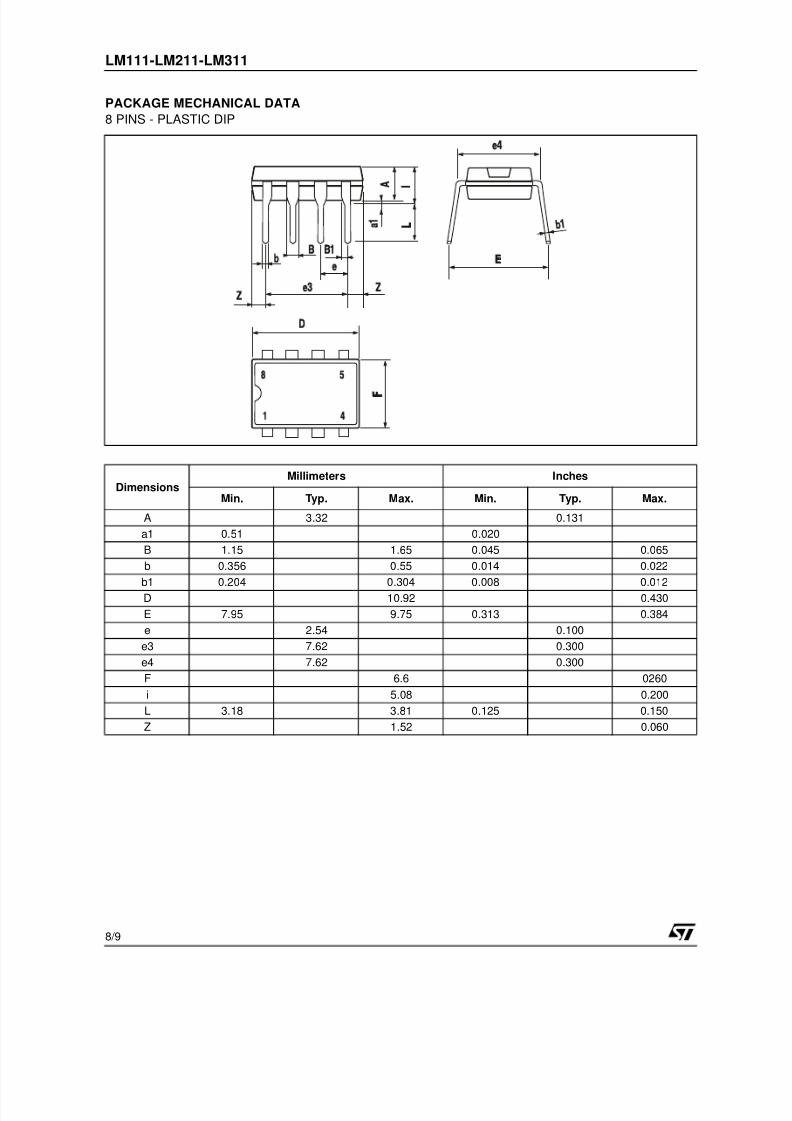
PACKAGE MECHANICAL DATA
8 PINS - PLASTIC DIP
DimensionsMillimeters Inches
Min. Typ. Max. Min. Typ. Max.
A 3.32 0.131
a1 0.51 0.020
B 1.15 1.65 0.045 0.065
b 0.356 0.55 0.014 0.022
b1 0.204 0.304 0.008 0.012
D 10.92 0.430
E 7.95 9.75 0.313 0.384
e 2.54 0.100
e3 7.62 0.300
e4 7.62 0.300
F 6.6 0260
i 5.08 0.200
L 3.18 3.81 0.125 0.150
Z 1.52 0.060

8/7/2019 LM311 IC Data sheet
http://slidepdf.com/reader/full/lm311-ic-data-sheet 9/10
LM111-LM211-LM311
9/9
PACKAGE MECHANICAL DATA
8 PINS - PLASTIC MICROPACKAGE (SO)
DimensionsMillimeters Inches
Min. Typ. Max. Min. Typ. Max.
A 1.75 0.069
a1 0.1 0.25 0.004 0.010
a2 1.65 0.065
a3 0.65 0.85 0.026 0.033
b 0.35 0.48 0.014 0.019
b1 0.19 0.25 0.007 0.010
C 0.25 0.5 0.010 0.020
c1 45° (typ.)
D 4.8 5.0 0.189 0.197
E 5.8 6.2 0.228 0.244
e 1.27 0.050
e3 3.81 0.150
F 3.8 4.0 0.150 0.157
L 0.4 1.27 0.016 0.050
M 0.6 0.024
S 8° (max.)
b
e3
Aa2
s
L
C
E
c1a3
b1
a1
D
M
8 5
1 4
F
Information furnished is believed to be accurate and reliable. However, STMicroelectronics assumes no responsibility for theconsequences of use of such information nor for any infringement of patents or other r ights of third parties which may result fromits use. No license is granted by implication or otherwise under any patent or patent rights of STMicroelectronics. Specificationsmentioned in this publication are subject to change without notice. This publication supersedes and replaces all informationpreviously supplied. STMicroelectronics products are not authorized for use as critical components in life support devices orsystems without express written approval of STMicroelectronics.
© The ST logo is a registered trademark of STMicroelectronics
© 2002 STMicroelectronics - Printed in Italy - All Rights ReservedSTMicroelectronics GROUP OF COMPANIES
Australia - Brazil - Canada - China - Finland - France - Germany - Hong Kong - India - Israel - Italy - Japan - MalaysiaMalta - Morocco - Singapore - Spain - Sweden - Switzerland - United Kingdom - United States
© http://www.st.com

8/7/2019 LM311 IC Data sheet
http://slidepdf.com/reader/full/lm311-ic-data-sheet 10/10
This datasheet has been download from:
www.datasheetcatalog.com
Datasheets for electronics components.