LM2825 Integrated Power Supply 1A DC-DC Converter · LM2825 Integrated Power Supply 1A DC-DC...
12
LM2825 Integrated Power Supply 1A DC-DC Converter General Description The LM2825 is a complete 1A DC-DC Buck converter pack- aged in a 24-lead molded Dual-In-Line integrated circuit package. Contained within the package are all the active and passive components for a high efficiency step-down (buck) switching regulator. Available in fixed output voltages of 3.3V, 5V and 12V, as well as two adjustable versions, these devices can provide up to 1A of load current with fully guaranteed electri- cal specifications. Self-contained, this converter is also fully protected from out- put fault conditions, such as excessive load current, short circuits, or excessive temperatures. Highlights n No external components required (fixed output voltage versions) n Integrated circuit reliability n MTBF over 20 million hours n Radiated EMI meets Class B stipulated by CISPR 22 n High power density, 35 W/in 3 n 24-pin DIP package profile (1.25 x 0.54 x 0.26 inches) Features n Minimum design time required n 3.3V, 5V and 12V fixed output versions n Two adjustable versions allow 1.23V to 15V outputs n Wide input voltage range, up to 40V n Low-power standby mode, I Q typically 65 μA n High efficiency, typically 80% n ±4% output voltage tolerance n Excellent line and load regulation n TTL shutdown capability/programmable Soft-start n Thermal shutdown and current limit protection n -40˚C to +85˚C ambient temperature range Applications n Simple high-efficiency step-down (buck) regulator n On-card switching regulators n Efficient pre-regulator for linear regulators n Distributed power systems n DC/DC module replacement Standard Application (Fixed output voltage versions) Radiated EMI Radiated emission of electromagnetic fields is measured at 10m distance. The emission levels are within the Class B limits stipulated by CISPR 22. 30....230 MHz 30 dB μV/m 230....1000 MHz 37 dB μV/m 1....10 GHz 46 dB μV/m Connection Diagram Ordering Information Order Number LM2825N-3.3, LM2825N-5.0, LM2825N-12, LM2825N-ADJ or LM2825HN-ADJ See NS Package Number NA24F DS012661-27 DS012661-1 DS012661-2 “NC (Do not use)” pins: See Figure 11. Top View May 1997 LM2825 Integrated Power Supply 1A DC-DC Converter © 1997 National Semiconductor Corporation DS012661 www.national.com
Transcript of LM2825 Integrated Power Supply 1A DC-DC Converter · LM2825 Integrated Power Supply 1A DC-DC...
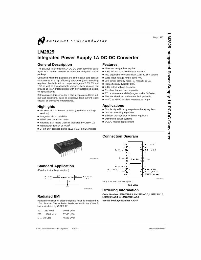
LM2825Integrated Power Supply 1A DC-DC ConverterGeneral DescriptionThe LM2825 is a complete 1A DC-DC Buck converter pack-aged in a 24-lead molded Dual-In-Line integrated circuitpackage.
Contained within the package are all the active and passivecomponents for a high efficiency step-down (buck) switchingregulator. Available in fixed output voltages of 3.3V, 5V and12V, as well as two adjustable versions, these devices canprovide up to 1A of load current with fully guaranteed electri-cal specifications.
Self-contained, this converter is also fully protected from out-put fault conditions, such as excessive load current, shortcircuits, or excessive temperatures.
Highlightsn No external components required (fixed output voltageversions)
n Integrated circuit reliabilityn MTBF over 20 million hoursn Radiated EMI meets Class B stipulated by CISPR 22n High power density, 35 W/in3
n 24-pin DIP package profile (1.25 x 0.54 x 0.26 inches)
Featuresn Minimum design time requiredn 3.3V, 5V and 12V fixed output versionsn Two adjustable versions allow 1.23V to 15V outputsn Wide input voltage range, up to 40Vn Low-power standby mode, IQ typically 65 µAn High efficiency, typically 80%n ±4% output voltage tolerancen Excellent line and load regulationn TTL shutdown capability/programmable Soft-startn Thermal shutdown and current limit protectionn −40˚C to +85˚C ambient temperature range
Applicationsn Simple high-efficiency step-down (buck) regulatorn On-card switching regulatorsn Efficient pre-regulator for linear regulatorsn Distributed power systemsn DC/DC module replacement
Standard Application(Fixed output voltage versions)
Radiated EMIRadiated emission of electromagnetic fields is measured at10m distance. The emission levels are within the Class Blimits stipulated by CISPR 22.
30. . . .230 MHz 30 dB µV/m
230. . . .1000 MHz 37 dB µV/m
1. . . .10 GHz 46 dB µV/m
Connection Diagram
Ordering InformationOrder Number LM2825N-3.3, LM2825N-5.0, LM2825N-12,LM2825N-ADJ or LM2825HN-ADJ
See NS Package Number NA24F
DS012661-27
DS012661-1
DS012661-2
“NC (Do not use)” pins: See Figure 11.
Top View
May 1997
LM2825
IntegratedPow
erSupply
1ADC-DCConverter
© 1997 National Semiconductor Corporation DS012661 www.national.com
Absolute Maximum Ratings (Note 1)
If Military/Aerospace specified devices are required,please contact the National Semiconductor Sales Office/Distributors for availability and specifications.
Maximum Input Supply (VIN) +45VSD/SS Pin Input Voltage (Note 2) 6VOutput Pin Voltage(3.3V, 5.0V and ADJ) −1V ≤ V ≤ 9V(12V and H-ADJ) −1V ≤ V ≤ 16V
ADJ Pin Voltage (ADJ, H-ADJ only) −0.3V ≤ V ≤ 25VPower Dissipation Internally LimitedStorage Temperature Range −40˚C to +125˚C
ESD SusceptibilityHuman Body Model (Note 3) 2 kV
Lead Temperature (Soldering 10 sec.) 260˚C
Operating RatingsAmbient Temperature Range −40˚C ≤ TA ≤ +85˚CJunction Temperature Range −40˚C ≤ TJ ≤ +125˚CInput Supply Voltage (3.3V version) 4.75V to 40VInput Supply Voltage (5V version) 7V to 40VInput Supply Voltage (12V version) 15V to 40VInput Supply Voltage (-ADJ, H-ADJ) 4.5V to 40V
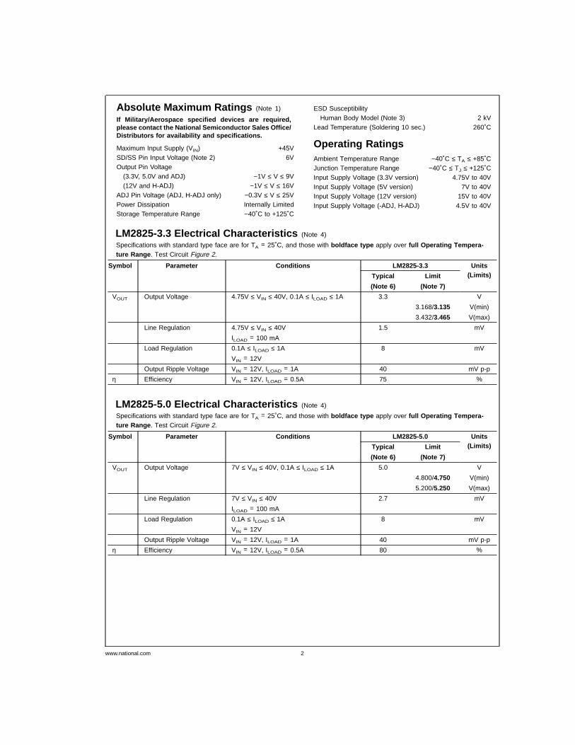
LM2825-3.3 Electrical Characteristics (Note 4)
Specifications with standard type face are for TA = 25˚C, and those with boldface type apply over full Operating Tempera-ture Range . Test Circuit Figure 2.
Symbol Parameter Conditions LM2825-3.3 Units(Limits)Typical Limit
(Note 6) (Note 7)
VOUT Output Voltage 4.75V ≤ VIN ≤ 40V, 0.1A ≤ ILOAD ≤ 1A 3.3 V
3.168/3.135 V(min)
3.432/3.465 V(max)
Line Regulation 4.75V ≤ VIN ≤ 40V 1.5 mV
ILOAD = 100 mA
Load Regulation 0.1A ≤ ILOAD ≤ 1A 8 mV
VIN = 12V
Output Ripple Voltage VIN = 12V, ILOAD = 1A 40 mV p-p
η Efficiency VIN = 12V, ILOAD = 0.5A 75 %
LM2825-5.0 Electrical Characteristics (Note 4)
Specifications with standard type face are for TA = 25˚C, and those with boldface type apply over full Operating Tempera-ture Range . Test Circuit Figure 2.
Symbol Parameter Conditions LM2825-5.0 Units(Limits)Typical Limit
(Note 6) (Note 7)
VOUT Output Voltage 7V ≤ VIN ≤ 40V, 0.1A ≤ ILOAD ≤ 1A 5.0 V
4.800/4.750 V(min)
5.200/5.250 V(max)
Line Regulation 7V ≤ VIN ≤ 40V 2.7 mV
ILOAD = 100 mA
Load Regulation 0.1A ≤ ILOAD ≤ 1A 8 mV
VIN = 12V
Output Ripple Voltage VIN = 12V, ILOAD = 1A 40 mV p-p
η Efficiency VIN = 12V, ILOAD = 0.5A 80 %
www.national.com 2
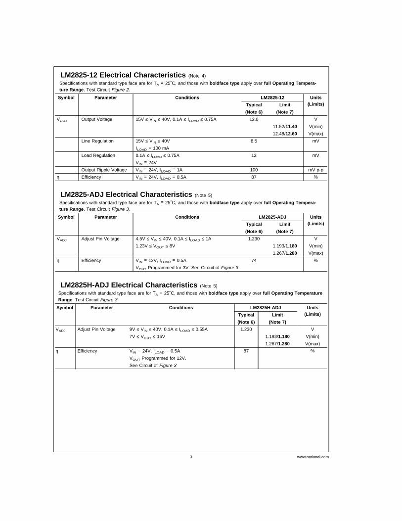
LM2825-12 Electrical Characteristics (Note 4)
Specifications with standard type face are for TA = 25˚C, and those with boldface type apply over full Operating Tempera-ture Range . Test Circuit Figure 2.
Symbol Parameter Conditions LM2825-12 Units(Limits)Typical Limit
(Note 6) (Note 7)
VOUT Output Voltage 15V ≤ VIN ≤ 40V, 0.1A ≤ ILOAD ≤ 0.75A 12.0 V
11.52/11.40 V(min)
12.48/12.60 V(max)
Line Regulation 15V ≤ VIN ≤ 40V 8.5 mV
ILOAD = 100 mA
Load Regulation 0.1A ≤ ILOAD ≤ 0.75A 12 mV
VIN = 24V
Output Ripple Voltage VIN = 24V, ILOAD = 1A 100 mV p-p
η Efficiency VIN = 24V, ILOAD = 0.5A 87 %
LM2825-ADJ Electrical Characteristics (Note 5)
Specifications with standard type face are for TA = 25˚C, and those with boldface type apply over full Operating Tempera-ture Range . Test Circuit Figure 3.
Symbol Parameter Conditions LM2825-ADJ Units(Limits)Typical Limit
(Note 6) (Note 7)
VADJ Adjust Pin Voltage 4.5V ≤ VIN ≤ 40V, 0.1A ≤ ILOAD ≤ 1A 1.230 V
1.23V ≤ VOUT ≤ 8V 1.193/1.180 V(min)
1.267/1.280 V(max)
η Efficiency VIN = 12V, ILOAD = 0.5A 74 %
VOUT Programmed for 3V. See Circuit of Figure 3
LM2825H-ADJ Electrical Characteristics (Note 5)
Specifications with standard type face are for TA = 25˚C, and those with boldface type apply over full Operating TemperatureRange . Test Circuit Figure 3.
Symbol Parameter Conditions LM2825H-ADJ Units(Limits)Typical Limit
(Note 6) (Note 7)
VADJ Adjust Pin Voltage 9V ≤ VIN ≤ 40V, 0.1A ≤ ILOAD ≤ 0.55A 1.230 V
7V ≤ VOUT ≤ 15V 1.193/1.180 V(min)
1.267/1.280 V(max)
η Efficiency VIN = 24V, ILOAD = 0.5A 87 %
VOUT Programmed for 12V.
See Circuit of Figure 3
3 www.national.com

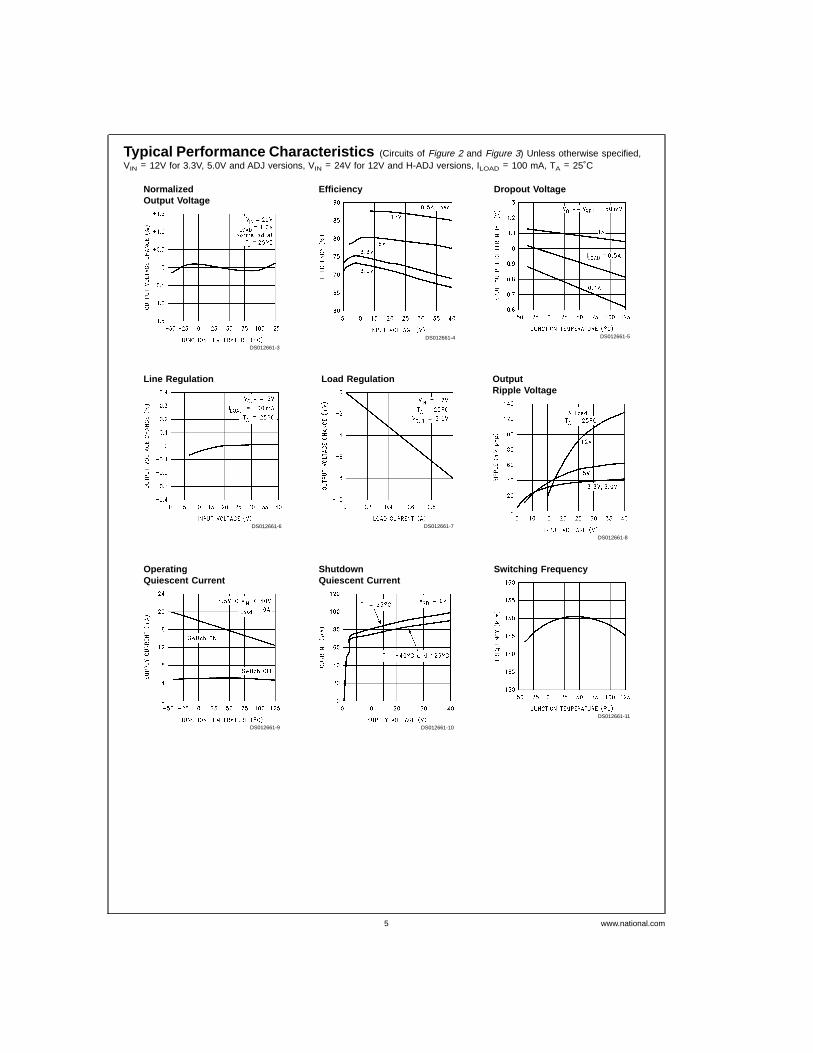
Typical Performance Characteristics (Circuits of Figure 2 and Figure 3) Unless otherwise specified,VIN = 12V for 3.3V, 5.0V and ADJ versions, VIN = 24V for 12V and H-ADJ versions, ILOAD = 100 mA, TA = 25˚C
NormalizedOutput Voltage
DS012661-3
Efficiency
DS012661-4
Dropout Voltage
DS012661-5
Line Regulation
DS012661-6
Load Regulation
DS012661-7
OutputRipple Voltage
DS012661-8
OperatingQuiescent Current
DS012661-9
ShutdownQuiescent Current
DS012661-10
Switching Frequency
DS012661-11
5 www.national.com
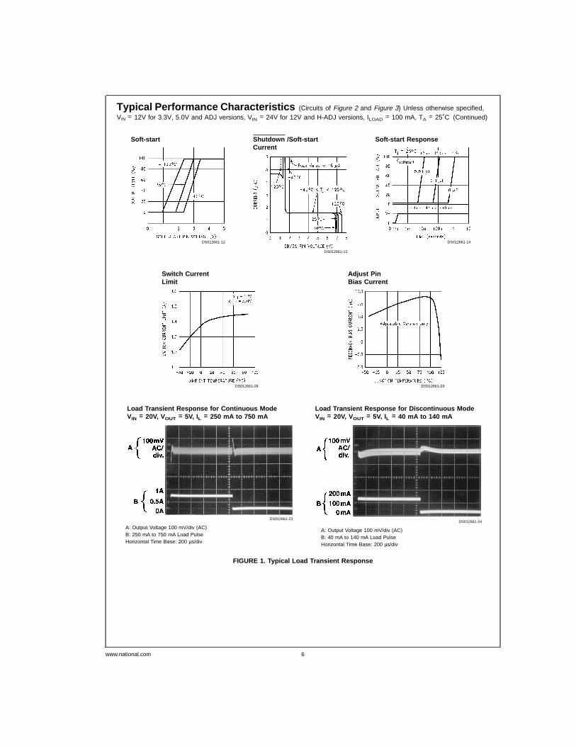
Typical Performance Characteristics (Circuits of Figure 2 and Figure 3) Unless otherwise specified,VIN = 12V for 3.3V, 5.0V and ADJ versions, VIN = 24V for 12V and H-ADJ versions, ILOAD = 100 mA, TA = 25˚C (Continued)
Soft-start
DS012661-12
Shutdown /Soft-startCurrent
DS012661-13
Soft-start Response
DS012661-14
Switch CurrentLimit
DS012661-28
Adjust PinBias Current
DS012661-29
Load Transient Response for Continuous ModeVIN = 20V, VOUT = 5V, IL = 250 mA to 750 mA
DS012661-23
A: Output Voltage 100 mV/div (AC)B: 250 mA to 750 mA Load PulseHorizontal Time Base: 200 µs/div
Load Transient Response for Discontinuous ModeVIN = 20V, VOUT = 5V, IL = 40 mA to 140 mA
DS012661-24
A: Output Voltage 100 mV/div (AC)B: 40 mA to 140 mA Load PulseHorizontal Time Base: 200 µs/div
FIGURE 1. Typical Load Transient Response
www.national.com 6
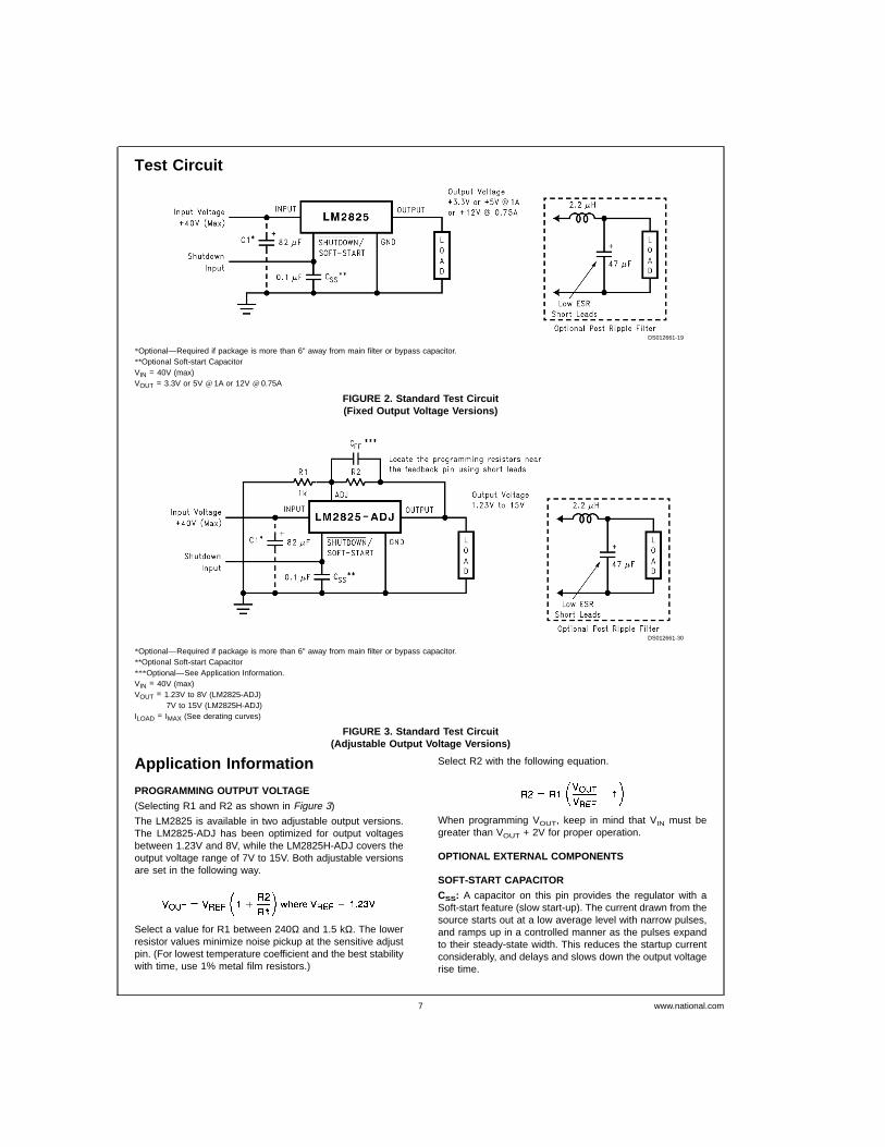
Test Circuit
Application Information
PROGRAMMING OUTPUT VOLTAGE
(Selecting R1 and R2 as shown in Figure 3)
The LM2825 is available in two adjustable output versions.The LM2825-ADJ has been optimized for output voltagesbetween 1.23V and 8V, while the LM2825H-ADJ covers theoutput voltage range of 7V to 15V. Both adjustable versionsare set in the following way.
Select a value for R1 between 240Ω and 1.5 kΩ. The lowerresistor values minimize noise pickup at the sensitive adjustpin. (For lowest temperature coefficient and the best stabilitywith time, use 1% metal film resistors.)
Select R2 with the following equation.
When programming VOUT, keep in mind that VIN must begreater than VOUT + 2V for proper operation.
OPTIONAL EXTERNAL COMPONENTS
SOFT-START CAPACITOR
CSS: A capacitor on this pin provides the regulator with aSoft-start feature (slow start-up). The current drawn from thesource starts out at a low average level with narrow pulses,and ramps up in a controlled manner as the pulses expandto their steady-state width. This reduces the startup currentconsiderably, and delays and slows down the output voltagerise time.
DS012661-19
*Optional—Required if package is more than 6" away from main filter or bypass capacitor.**Optional Soft-start CapacitorVIN = 40V (max)VOUT = 3.3V or 5V @ 1A or 12V @ 0.75A
FIGURE 2. Standard Test Circuit(Fixed Output Voltage Versions)
DS012661-30
*Optional—Required if package is more than 6" away from main filter or bypass capacitor.**Optional Soft-start Capacitor***Optional—See Application Information.VIN = 40V (max)VOUT = 1.23V to 8V (LM2825-ADJ)
7V to 15V (LM2825H-ADJ)ILOAD = IMAX (See derating curves)
FIGURE 3. Standard Test Circuit(Adjustable Output Voltage Versions)
7 www.national.com
Application Information (Continued)
It is especially useful in situations where the input powersource is limited in the amount of current it can deliver, sinceyou avoid loading down this type of power supply.
Under some operating conditions, a Soft-start capacitor isrequired for proper operation. Figure 5 indicates the inputvoltage and ambient temperature conditions for which aSoft-start capacitor may be required.
This curve is typical for full guaranteed output current andcan be used as a guideline. As the output current decreases,the operating area requiring a Soft-start capacitor de-creases. Capacitor values between 0.1 µF and 1 µF are rec-ommended. Tantalum or ceramic capacitors are appropriatefor this application.
INPUT CAPACITOR
CIN: An optional input capacitor is required if the package ismore than 6" away from the main filter or bypass capacitor. Alow ESR aluminum or tantalum bypass capacitor is recom-mended between the input pin and ground to prevent largevoltage transients from appearing at the input. In addition, tobe conservative, the RMS current rating of the input capaci-tor should be selected to be at least 1⁄2 the DC load current.With a 1A load, a capacitor with a RMS current rating of atleast 500 mA is recommended.
The voltage rating should be approximately 1.25 times themaximum input voltage. With a nominal input voltage of 12V,an aluminum electrolytic capacitor (Panasonic HFQ series orNichicon PL series or equivalent) with a voltage ratinggreater than 15V (1.25 x VIN) would be needed.
Solid tantalum input capacitors should only be used wherethe input source is impedance current limited. High dV/dt ap-plied at the input can cause excessive charge currentthrough low ESR tantalum capacitors. This high charge cur-rent can result in shorting within the capacitor. It is recom-mended that they be surge current tested by the manufactur-er.The TPS series available from AVX, and the 593D seriesfrom Sprague are both surge current tested.
Use caution when using ceramic capacitors for input bypass-ing, because it may cause ringing at the VIN pin.
LOWERING OUTPUT RIPPLE
When using the adjustable parts, one can achieve lower out-put ripple voltage by shorting a resistor internal to theLM2825. However, if this resistor is shorted, a feed forwardcapacitor must be used to keep the regulator stable. For thisreason, this resistor must be left open on all of the fixed out-put voltage versions or instability will result. See the feed for-ward capacitor selection below. Shorting the internal resistoris accomplished by shorting pins 8 and 9 on the LM2825,and will typically reduce output ripple by 25 to 33%.
FEED FORWARD CAPACITOR SELECTION (C FF)
When using an adjustable part and pins 8 and 9 are shortedto reduce output ripple, a feed forward capacitor is required.This capacitor is typically between 680 pF and 2700 pF. Thetable of Figure 4 shows the value for CFF for a given outputvoltage and feedback resistor R2 (R1 = 1 kΩ).
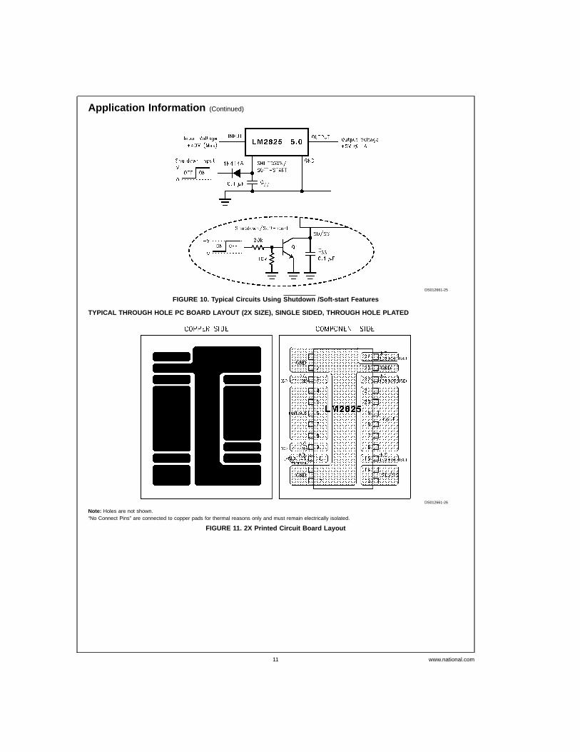
SHUTDOWN
The circuit shown in Figure 10 shows 2 circuits for theShutdown/Soft-start feature using different logic signals forshutdown and using a 0.1 µF Soft-start capacitor.
THERMAL CONSIDERATIONS
The LM2825 is available in a 24-pin through hole DIP. Thepackage is molded plastic with a copper lead frame. Whenthe package is soldered to the PC board, the copper and theboard are the heat sink for the LM2825.
VOUT R2 CFF
LM2825-ADJ
2 630 N/A
3 1.43k N/A
4 2.26k 2700 pF
5 3.09k 2700 pF
6 3.92k 2200 pF
7 4.75k 1800 pF
8 5.49k 1500 pF
LM2825H-ADJ
7 4.75k 2700 pF
8 5.49k 2200 pF
9 6.34k 1800 pF
10 7.15k 1500 pF
11 8.06k 1000 pF
12 8.87k 820 pF
13 9.53k 680 pF
14 10.5k 680 pF
15 11.3k 680 pF
FIGURE 4. CFF Selection Table
DS012661-22
FIGURE 5. Usage of the Soft-start Capacitor
www.national.com 8
Application Information (Continued)
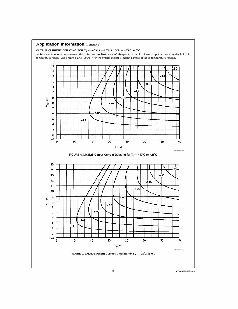
OUTPUT CURRENT DERATING FOR TJ = −40˚C to −25˚C AND T J = −25˚C to 0˚C
At the lower temperature extremes, the switch current limit drops off sharply. As a result, a lower output current is available in thistemperature range. See Figure 6 and Figure 7 for the typical available output current at these temperature ranges.
DS012661-32
FIGURE 6. LM2825 Output Current Derating for T J = −40˚C to −25˚C
DS012661-33
FIGURE 7. LM2825 Output Current Derating for T J = −25˚C to 0˚C
9 www.national.com
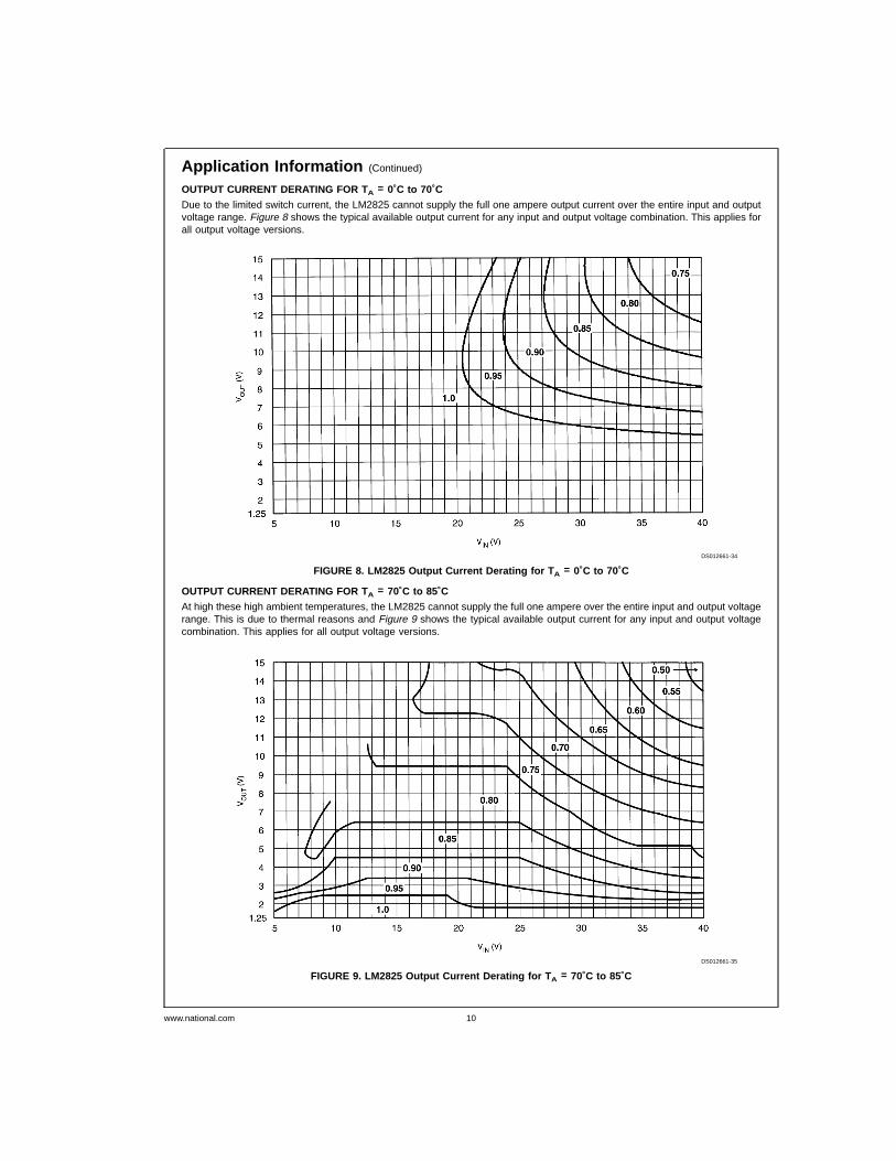
Application Information (Continued)
OUTPUT CURRENT DERATING FOR TA = 0˚C to 70˚C
Due to the limited switch current, the LM2825 cannot supply the full one ampere output current over the entire input and outputvoltage range. Figure 8 shows the typical available output current for any input and output voltage combination. This applies forall output voltage versions.
OUTPUT CURRENT DERATING FOR TA = 70˚C to 85˚C
At high these high ambient temperatures, the LM2825 cannot supply the full one ampere over the entire input and output voltagerange. This is due to thermal reasons and Figure 9 shows the typical available output current for any input and output voltagecombination. This applies for all output voltage versions.
DS012661-34
FIGURE 8. LM2825 Output Current Derating for T A = 0˚C to 70˚C
DS012661-35
FIGURE 9. LM2825 Output Current Derating for T A = 70˚C to 85˚C
www.national.com 10
Application Information (Continued)
TYPICAL THROUGH HOLE PC BOARD LAYOUT (2X SIZE), SINGLE SIDED, THROUGH HOLE PLATED
DS012661-25
FIGURE 10. Typical Circuits Using Shutdown /Soft-start Features
DS012661-26
Note: Holes are not shown.“No Connect Pins” are connected to copper pads for thermal reasons only and must remain electrically isolated.
FIGURE 11. 2X Printed Circuit Board Layout
11 www.national.com
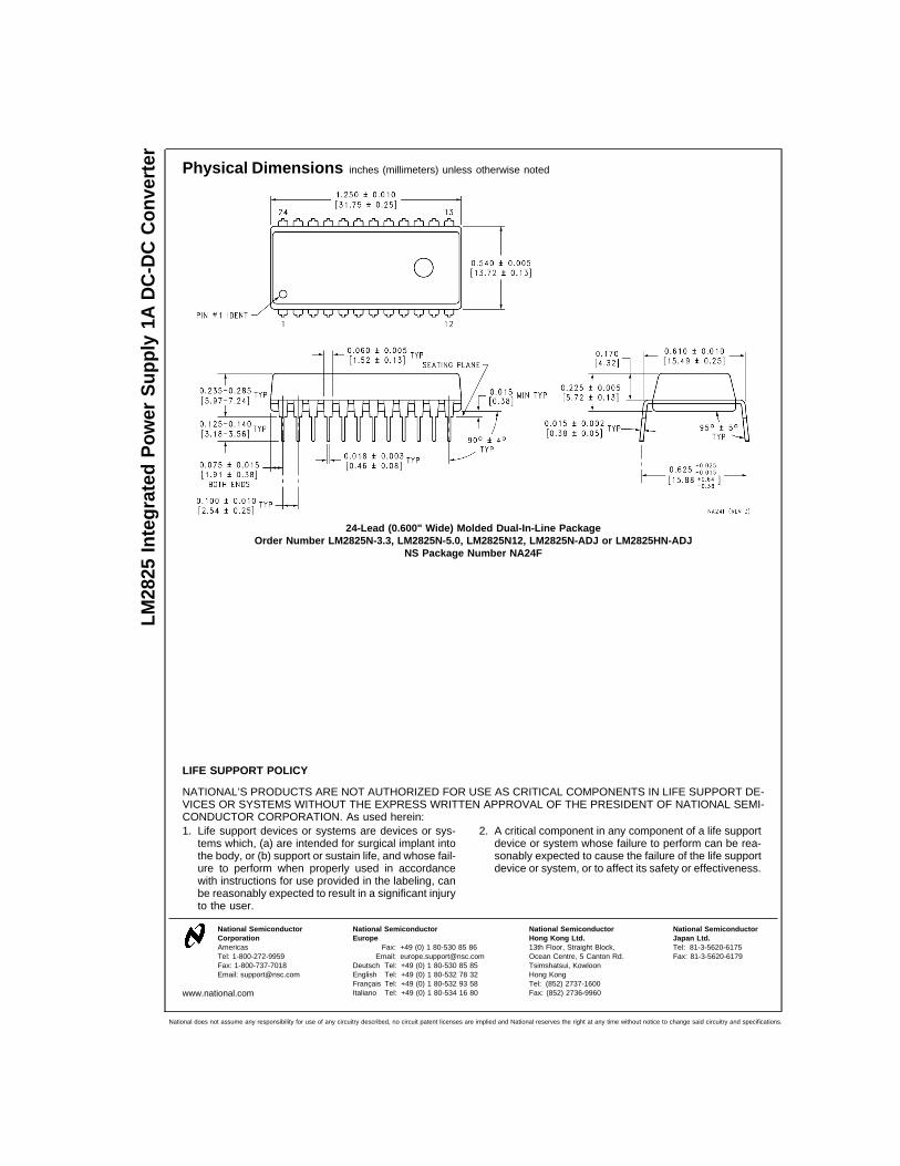
Physical Dimensions inches (millimeters) unless otherwise noted
LIFE SUPPORT POLICY
NATIONAL’S PRODUCTS ARE NOT AUTHORIZED FOR USE AS CRITICAL COMPONENTS IN LIFE SUPPORT DE-VICES OR SYSTEMS WITHOUT THE EXPRESS WRITTEN APPROVAL OF THE PRESIDENT OF NATIONAL SEMI-CONDUCTOR CORPORATION. As used herein:1. Life support devices or systems are devices or sys-
tems which, (a) are intended for surgical implant intothe body, or (b) support or sustain life, and whose fail-ure to perform when properly used in accordancewith instructions for use provided in the labeling, canbe reasonably expected to result in a significant injuryto the user.
2. A critical component in any component of a life supportdevice or system whose failure to perform can be rea-sonably expected to cause the failure of the life supportdevice or system, or to affect its safety or effectiveness.
National SemiconductorCorporationAmericasTel: 1-800-272-9959Fax: 1-800-737-7018Email: [email protected]
www.national.com
National SemiconductorEurope
Fax: +49 (0) 1 80-530 85 86Email: [email protected]
Deutsch Tel: +49 (0) 1 80-530 85 85English Tel: +49 (0) 1 80-532 78 32Français Tel: +49 (0) 1 80-532 93 58Italiano Tel: +49 (0) 1 80-534 16 80
National SemiconductorHong Kong Ltd.13th Floor, Straight Block,Ocean Centre, 5 Canton Rd.Tsimshatsui, KowloonHong KongTel: (852) 2737-1600Fax: (852) 2736-9960
National SemiconductorJapan Ltd.Tel: 81-3-5620-6175Fax: 81-3-5620-6179
24-Lead (0.600" Wide) Molded Dual-In-Line PackageOrder Number LM2825N-3.3, LM2825N-5.0, LM2825N12, LM2825N-ADJ or LM2825HN-ADJ
NS Package Number NA24F
LM2825
Integrated
Pow
erSupply1A
DC-DCConverter
National does not assume any responsibility for use of any circuitry described, no circuit patent licenses are implied and National reserves the right at any time without notice to change said circuitry and specifications.