LM1949 Injector Drive Controller (Rev. C)
17
LM1949 www.ti.com SNLS349C – FEB 1995 – REVISED MARCH 2013 LM1949 Injector Drive Controller Check for Samples: LM1949 1FEATURES DESCRIPTION The LM1949 linear integrated circuit serves as an 2• Low Voltage Supply (3V–5.5V) excellent control of fuel injector drive circuitry in • 22 mA Output Drive Current modern automotive systems. The IC is designed to • No RFI Radiation control an external power NPN Darlington transistor that drives the high current injector solenoid. The • Adaptable to All Injector Current Levels current required to open a solenoid is several times • Highly Accurate Operation greater than the current necessary to merely hold it • TTL/CMOS Compatible Input Logic Levels open; therefore, the LM1949, by directly sensing the actual solenoid current, initially saturates the driver • Short Circuit Protection until the “peak” injector current is four times that of • High Impedance Input the idle or “holding” current (Figure 19–Figure 22). • Externally Set Holding Current, I H This guarantees opening of the injector. The current is then automatically reduced to the sufficient holding • Internally Set Peak Current (4 × I H ) level for the duration of the input pulse. In this way, • Externally Set Time-Out the total power consumed by the system is • Can be Modified for Full Switching Operation dramatically reduced. Also, a higher degree of • Available in Plastic 8-Pin PDIP correlation of fuel to the input voltage pulse (or duty cycle) is achieved, since opening and closing delays of the solenoid will be reduced. APPLICATIONS Normally powered from a 5V ± 10% supply, the IC is • Fuel Injection typically operable over the entire temperature range • Throttle Body Injection (−55°C to +125°C ambient) with supplies as low as 3 • Solenoid Controls volts. This is particularly useful under “cold crank” • Air and Fluid Valves conditions when the battery voltage may drop low enough to deregulate the 5-volt power supply. • DC Motor Drives The LM1949 is available in the plastic PDIP, (contact factory for other package options). Typical Application Figure 1. Typical Application and Test Circuit 1 Please be aware that an important notice concerning availability, standard warranty, and use in critical applications of Texas Instruments semiconductor products and disclaimers thereto appears at the end of this data sheet. 2All trademarks are the property of their respective owners. PRODUCTION DATA information is current as of publication date. Copyright © 1995–2013, Texas Instruments Incorporated Products conform to specifications per the terms of the Texas Instruments standard warranty. Production processing does not necessarily include testing of all parameters.
-
Upload
truongthuy -
Category
Documents
-
view
230 -
download
0
Transcript of LM1949 Injector Drive Controller (Rev. C)

LM1949
www.ti.com SNLS349C –FEB 1995–REVISED MARCH 2013
LM1949 Injector Drive ControllerCheck for Samples: LM1949
1FEATURES DESCRIPTIONThe LM1949 linear integrated circuit serves as an
2• Low Voltage Supply (3V–5.5V)excellent control of fuel injector drive circuitry in
• 22 mA Output Drive Current modern automotive systems. The IC is designed to• No RFI Radiation control an external power NPN Darlington transistor
that drives the high current injector solenoid. The• Adaptable to All Injector Current Levelscurrent required to open a solenoid is several times• Highly Accurate Operation greater than the current necessary to merely hold it
• TTL/CMOS Compatible Input Logic Levels open; therefore, the LM1949, by directly sensing theactual solenoid current, initially saturates the driver• Short Circuit Protectionuntil the “peak” injector current is four times that of• High Impedance Inputthe idle or “holding” current (Figure 19–Figure 22).
• Externally Set Holding Current, IH This guarantees opening of the injector. The currentis then automatically reduced to the sufficient holding• Internally Set Peak Current (4 × IH)level for the duration of the input pulse. In this way,• Externally Set Time-Outthe total power consumed by the system is
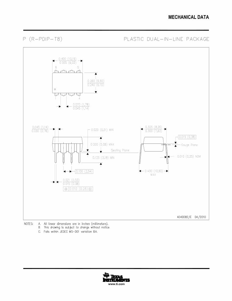
• Can be Modified for Full Switching Operation dramatically reduced. Also, a higher degree of• Available in Plastic 8-Pin PDIP correlation of fuel to the input voltage pulse (or duty
cycle) is achieved, since opening and closing delaysof the solenoid will be reduced.APPLICATIONSNormally powered from a 5V ± 10% supply, the IC is• Fuel Injectiontypically operable over the entire temperature range• Throttle Body Injection(−55°C to +125°C ambient) with supplies as low as 3
• Solenoid Controls volts. This is particularly useful under “cold crank”• Air and Fluid Valves conditions when the battery voltage may drop low
enough to deregulate the 5-volt power supply.• DC Motor DrivesThe LM1949 is available in the plastic PDIP, (contactfactory for other package options).
Typical Application
Figure 1. Typical Application and Test Circuit1
Please be aware that an important notice concerning availability, standard warranty, and use in critical applications ofTexas Instruments semiconductor products and disclaimers thereto appears at the end of this data sheet.
2All trademarks are the property of their respective owners.
PRODUCTION DATA information is current as of publication date. Copyright © 1995–2013, Texas Instruments IncorporatedProducts conform to specifications per the terms of the TexasInstruments standard warranty. Production processing does notnecessarily include testing of all parameters.

IN
OUT
COMP
SENSEINPUT
TIMER
SENSEGND
SUPPLY
SUPPLYGND
1
2
3
4 5
6
7
8LM
1949N
LM1949
SNLS349C –FEB 1995–REVISED MARCH 2013 www.ti.com
Figure 2. Package Number P0008E
These devices have limited built-in ESD protection. The leads should be shorted together or the device placed in conductive foamduring storage or handling to prevent electrostatic damage to the MOS gates.
Absolute Maximum Ratings (1) (2)
Supply Voltage 8V
Power Dissipation (3) 1235 mW
Input Voltage Range −0.3V to VCC
Operating Temperature Range −40°C to +125°C
Storage Temperature Range −65°C to +150°C
Junction Temperature 150°C
Lead Temp. (Soldering 10 sec.) 260°C
(1) Absolute Maximum Ratings indicate limits beyond which damage to the device may occur.(2) If Military/Aerospace specified devices are required, please contact the Texas Instruments Sales Office/ Distributors for availability and
specifications.(3) For operation in ambient temperatures above 25°C, the device must be derated based on a 150°C maximum junction temperature and a
thermal resistance of 100°C/W junction to ambient.
Electrical Characteristics(VCC = 5.5V, VIN = 2.4V, TJ = 25°C, Figure 1, unless otherwise specified.)
Symbol Parameter Conditions Min Typ Max Units
ICC Supply Current
Off VIN = 0V 11 23 mA
Peak Pin 8 = 0V 28 54 mA
Hold Pin 8 Open 16 26 mA
VOH Input On Level VCC = 5.5V 1.4 2.4 V
VCC = 3.0V 1.2 1.6 V
VOL Input Off Level VCC = 5.5V 1.0 1.35 V
VCC = 3.0V 0.7 1.15 V
IB Input Current −25 3 +25 µA
IOP Output Current
Peak Pin 8 = 0V −10 −22 mA
Hold Pin 8 Open −1.5 −5 mA
VS Output Saturation Voltage 10 mA, VIN = 0V 0.2 0.4 V
VP Sense Input
Peak Threshold VCC = 4.75V 350 386 415 mV
VH Hold Reference 88 94 102 mV
t Time-out, t t ÷ RTCT 90 100 110 %
2 Submit Documentation Feedback Copyright © 1995–2013, Texas Instruments Incorporated
Product Folder Links: LM1949

LM1949
www.ti.com SNLS349C –FEB 1995–REVISED MARCH 2013
Typical Performance Characteristics
Output Current vs Supply Current vsSupply Voltage Supply Voltage
Figure 3. Figure 4.
Quiescent Current vs Input Voltage ThresholdsSupply Voltage vs Supply Voltage
Figure 5. Figure 6.
Sense Input Peak Voltage Sense Input Hold Voltagevs Supply Voltage vs Supply Voltage
Figure 7. Figure 8.
Copyright © 1995–2013, Texas Instruments Incorporated Submit Documentation Feedback 3
Product Folder Links: LM1949
LM1949
SNLS349C –FEB 1995–REVISED MARCH 2013 www.ti.com
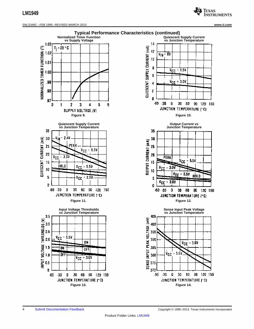
Typical Performance Characteristics (continued)Normalized Timer Function Quiescent Supply Current
vs Supply Voltage vs Junction Temperature
Figure 9. Figure 10.
Quiescent Supply Current Output Current vsvs Junction Temperature Junction Temperature
Figure 11. Figure 12.
Input Voltage Thresholds Sense Input Peak Voltagevs Junction Temperature vs Junction Temperature
Figure 13. Figure 14.
4 Submit Documentation Feedback Copyright © 1995–2013, Texas Instruments Incorporated
Product Folder Links: LM1949

LM1949
www.ti.com SNLS349C –FEB 1995–REVISED MARCH 2013
Typical Performance Characteristics (continued)Sense Input Hold Voltage Normalized Timer Functionvs Junction Temperature vs Junction Temperature
Figure 15. Figure 16.
LM1949N JunctionTemperature Rise Above
Ambientvs
Supply Voltage
Figure 17.
Copyright © 1995–2013, Texas Instruments Incorporated Submit Documentation Feedback 5
Product Folder Links: LM1949

LM1949
SNLS349C –FEB 1995–REVISED MARCH 2013 www.ti.com
Typical Circuit Waveforms
Figure 18.
APPLICATION HINTS
The injector driver integrated circuits were designed to be used in conjunction with an external controller. TheLM1949 derives its input signal from either a control oriented processor (COPS™), microprocessor, or someother system. This input signal, in the form of a square wave with a variable duty cycle and/or variable frequency,is applied to Pin 1. In a typical system, input frequency is proportional to engine RPM. Duty cycle is proportionalto the engine load. The circuits discussed are suitable for use in either open or closed loop systems. In closedloop systems, the engine exhaust is monitored and the air-to-fuel mixture is varied (via the duty cycle) tomaintain a perfect, or stochiometric, ratio.
INJECTORS
Injectors and solenoids are available in a vast array of sizes and characteristics. Therefore, it is necessary to beable to design a drive system to suit each type of solenoid. The purpose of this section is to enable any systemdesigner to use and modify the LM1949 and associated circuitry to meet the system specifications.
Fuel injectors can usually be modeled by a simple RL circuit. Figure 19 shows such a model for a typical fuelinjector. In actual operation, the value of L1 will depend upon the status of the solenoid. In other words, L1 willchange depending upon whether the solenoid is open or closed. This effect, if pronounced enough, can be avaluable aid in determining the current necessary to open a particular type of injector. The change in inductancemanifests itself as a breakpoint in the initial rise of solenoid current. The waveforms at the sense input show thisoccurring at approximately 130 mV. Thus, the current necessary to overcome the constrictive forces of thatparticular injector is 1.3 amperes.
Figure 19. Model of a Typical Fuel Injector
6 Submit Documentation Feedback Copyright © 1995–2013, Texas Instruments Incorporated
Product Folder Links: LM1949

LM1949
www.ti.com SNLS349C –FEB 1995–REVISED MARCH 2013
PEAK AND HOLD CURRENTS
The peak and hold currents are determined by the value of the sense resistor RS. The driver IC, when initiated bya logic 1 signal at Pin 1, initially drives Darlington transistor Q1 into saturation. The injector current will riseexponentially from zero at a rate dependent upon L1, R1, the battery voltage and the saturation voltage of Q1.The drop across the sense resistor is created by the solenoid current, and when this drop reaches the peakthreshold level, typically 385 mV, the IC is tripped from the peak state into the hold state. The IC now behavesmore as an op amp and drives Q1 within a closed loop system to maintain the hold reference voltage, typically 94mV, across RS. Once the injector current drops from the peak level to the hold level, it remains there for theduration of the input signal at Pin 1. This mode of operation is preferable when working with solenoids, since thecurrent required to overcome kinetic and constriction forces is often a factor of four or more times the currentnecessary to hold the injector open. By holding the injector current at one fourth of the peak current, powerdissipation in the solenoids and Q1 is reduced by at least the same factor.
In the circuit of Figure 1, it was known that the type of injector shown opens when the current exceeds 1.3 ampsand closes when the current then falls below 0.3 amps. In order to guarantee injector operation over the life andtemperature range of the system, a peak current of approximately 4 amps was chosen. This led to a value of RSof 0.1Ω. Dividing the peak and hold thresholds by this factor gives peak and hold currents through the solenoid of3.85 amps and 0.94 amps respectively.
Different types of solenoids may require different values of current. The sense resistor RS may be changedaccordingly. An 8-amp peak injector would use RS equal to .05Ω, etc. Note that for large currents above oneamp, IR drops within the component leads or printed circuit board may create substantial errors unlessappropriate care is taken. The sense input and sense ground leads (Pins 4 and 5 respectively), should be Kelvinconnected to RS. High current should not be allowed to flow through any part of these traces or connections. Aneasy solution to this problem on double-sided PC boards (without plated-through holes) is to have the highcurrent trace and sense trace attach to the RS lead from opposite sides of the board.
TIMER FUNCTION
The purpose of the timer function is to limit the power dissipated by the injector or solenoid under certainconditions. Specifically, when the battery voltage is low due to engine cranking, or just undercharged, there maynot be sufficient voltage available for the injector to achieve the peak current. In the Figure 18 waveforms underthe low battery condition, the injector current can be seen to be leveling out at 3 amps, or 1 amp below thenormal threshold. Since continuous operation at 3 amps may overheat the injectors, the timer function on the ICwill force the transition into the hold state after one time constant (the time constant is equal to RTx CT), or whenthe voltage on the TIMER pin (Pin 8) is greater than typically VSUPPLY x 63%. The timer is reset at the end ofeach input pulse. For systems where the timer function is not needed, it can be disabled by grounding the TIMERPin (Pin 8). For systems where the initial peak state is not required, (i.e., where the solenoid current risesimmediately to the hold level), the timer can be used to disable the peak function. This is done by setting the timeconstant equal to zero, (i.e., CT = 0). Leaving RT in place is recommended. The timer will then complete its time-out and disable the peak condition before the solenoid current has had a chance to rise above the hold level.
The actual range of the timer in injection systems will probably never vary much from the 3.9 milliseconds shownin Figure 1. However, the actual useful range of the timer extends from microseconds to seconds, depending onthe component values chosen. The useful range of RT is approximately 1k to 240k. The capacitor CT is limitedonly by stray capacitances for low values and by leakages for large values.
The timing capacitor is reset (discharged) when the IN pin (Pin 1) is below the VOL(MIN) threshold. The capacitorreset time at the end of each controller pulse is determined by the supply voltage and the timing capacitor value.The IC resets the capacitor to an initial voltage (VBE) by discharging it with a current of approximately 15 mA.Thus, a 0.1 µF cap is reset in approximately 25 µs.
COMPENSATION
Compensation of the error amplifier provides stability for the circuit during the hold state. External compensation(from Pin 2 to Pin 3) allows each design to be tailored for the characteristics of the system and/or type ofDarlington power device used. In the vast majority of designs, the value or type of the compensation capacitor isnot critical. Values of 100 pF to 0.1 µF work well with the circuit of Figure 1. The value shown of 0.1 µF (disc)provides a close optimum in choice between economy, speed, and noise immunity. In some systems, increasedphase and gain margin may be acquired by bypassing the collector of Q1 to ground with an appropriately rated0.1 µF capacitor. This is, however, rarely necessary.
Copyright © 1995–2013, Texas Instruments Incorporated Submit Documentation Feedback 7
Product Folder Links: LM1949
LM1949
SNLS349C –FEB 1995–REVISED MARCH 2013 www.ti.com
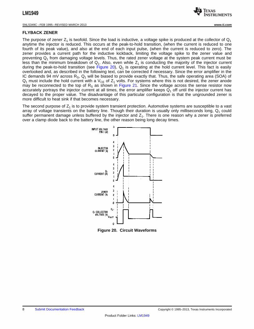
FLYBACK ZENER
The purpose of zener Z1 is twofold. Since the load is inductive, a voltage spike is produced at the collector of Q1anytime the injector is reduced. This occurs at the peak-to-hold transition, (when the current is reduced to onefourth of its peak value), and also at the end of each input pulse, (when the current is reduced to zero). Thezener provides a current path for the inductive kickback, limiting the voltage spike to the zener value andpreventing Q1 from damaging voltage levels. Thus, the rated zener voltage at the system peak current must beless than the minimum breakdown of Q1. Also, even while Z1 is conducting the majority of the injector currentduring the peak-to-hold transition (see Figure 20), Q1 is operating at the hold current level. This fact is easilyoverlooked and, as described in the following text, can be corrected if necessary. Since the error amplifier in theIC demands 94 mV across RS, Q1 will be biased to provide exactly that. Thus, the safe operating area (SOA) ofQ1 must include the hold current with a VCE of Z1 volts. For systems where this is not desired, the zener anodemay be reconnected to the top of RS as shown in Figure 21. Since the voltage across the sense resistor nowaccurately portrays the injector current at all times, the error amplifier keeps Q1 off until the injector current hasdecayed to the proper value. The disadvantage of this particular configuration is that the ungrounded zener ismore difficult to heat sink if that becomes necessary.
The second purpose of Z1 is to provide system transient protection. Automotive systems are susceptible to a vastarray of voltage transients on the battery line. Though their duration is usually only milliseconds long, Q1 couldsuffer permanent damage unless buffered by the injector and Z1. There is one reason why a zener is preferredover a clamp diode back to the battery line, the other reason being long decay times.
Figure 20. Circuit Waveforms
8 Submit Documentation Feedback Copyright © 1995–2013, Texas Instruments Incorporated
Product Folder Links: LM1949

LM1949
www.ti.com SNLS349C –FEB 1995–REVISED MARCH 2013
Figure 21. Alternate Configuration for Zener Z1
POWER DISSIPATION
The power dissipation of the system shown in Figure 1 is dependent upon several external factors, including thefrequency and duty cycle of the input waveform to Pin 1. Calculations are made more difficult since there aremany discontinuities and breakpoints in the power waveforms of the various components, most notably at thepeak-to-hold transition. Some generalizations can be made for normal operation. For example, in a typical cycleof operation, the majority of dissipation occurs during the hold state. The hold state is usually much longer thanthe peak state, and in the peak state nearly all power is stored as energy in the magnetic field of the injector,later to be dumped mostly through the zener. While this assumption is less accurate in the case of low batteryvoltage, it nevertheless gives an unexpectedly accurate set of approximations for general operation.
The following nomenclature refers to Figure 1. Typical values are given in parentheses:
RS = Sense Resistor (0, 1Ω)
VH = Sense Input Hold Voltage (.094V)
VP = Sense Input Peak Voltage (.385V)
VZ = Z1 Zener Breakdown Voltage (33V)
VBATT = Battery Voltage (14V)
L1 = Injector Inductance (.002H)
R1 = Injector Resistance (1Ω)
n = Duty Cycle of Input Voltage of Pin 1 (0 to 1)
f = Frequency of Input (10 Hz to 200 Hz)
Copyright © 1995–2013, Texas Instruments Incorporated Submit Documentation Feedback 9
Product Folder Links: LM1949
LM1949
SNLS349C –FEB 1995–REVISED MARCH 2013 www.ti.com
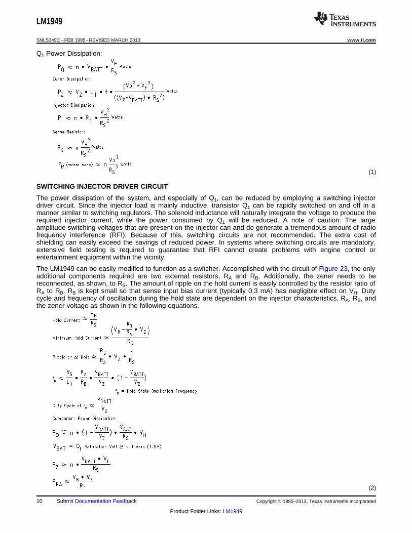
Q1 Power Dissipation:
(1)
SWITCHING INJECTOR DRIVER CIRCUIT
The power dissipation of the system, and especially of Q1, can be reduced by employing a switching injectordriver circuit. Since the injector load is mainly inductive, transistor Q1 can be rapidly switched on and off in amanner similar to switching regulators. The solenoid inductance will naturally integrate the voltage to produce therequired injector current, while the power consumed by Q1 will be reduced. A note of caution: The largeamplitude switching voltages that are present on the injector can and do generate a tremendous amount of radiofrequency interference (RFI). Because of this, switching circuits are not recommended. The extra cost ofshielding can easily exceed the savings of reduced power. In systems where switching circuits are mandatory,extensive field testing is required to guarantee that RFI cannot create problems with engine control orentertainment equipment within the vicinity.
The LM1949 can be easily modified to function as a switcher. Accomplished with the circuit of Figure 23, the onlyadditional components required are two external resistors, RA and RB. Additionally, the zener needs to bereconnected, as shown, to RS. The amount of ripple on the hold current is easily controlled by the resistor ratio ofRA to RB. RB is kept small so that sense input bias current (typically 0.3 mA) has negligible effect on VH. Dutycycle and frequency of oscillation during the hold state are dependent on the injector characteristics, RA, RB, andthe zener voltage as shown in the following equations.
(2)
10 Submit Documentation Feedback Copyright © 1995–2013, Texas Instruments Incorporated
Product Folder Links: LM1949

LM1949
www.ti.com SNLS349C –FEB 1995–REVISED MARCH 2013
As shown, the power dissipation by Q1 in this manner is substantially reduced. Measurements made with athermocouple on the bench indicated better than a fourfold reduction in power in Q1. However, the powerdissipation of the zener (which is independent of the zener voltage chosen) is increased over the circuit ofFigure 1.
Figure 22. Switching Application Circuit
Copyright © 1995–2013, Texas Instruments Incorporated Submit Documentation Feedback 11
Product Folder Links: LM1949
LM1949
SNLS349C –FEB 1995–REVISED MARCH 2013 www.ti.com
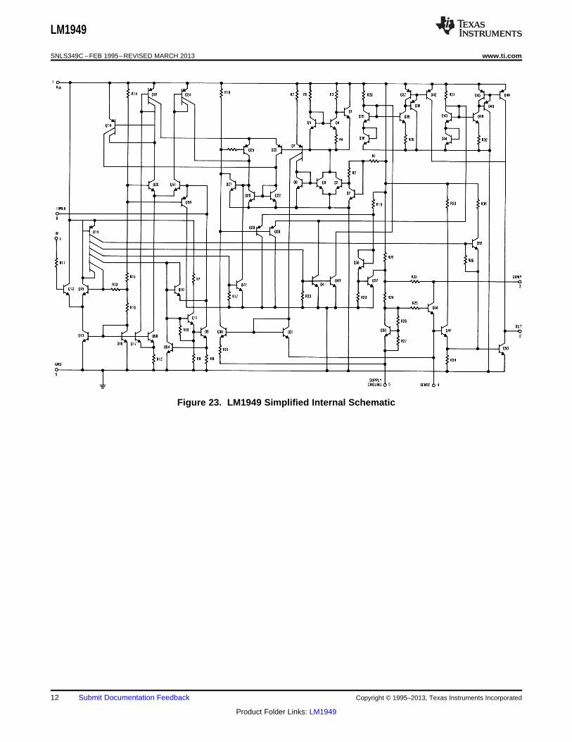
Figure 23. LM1949 Simplified Internal Schematic
12 Submit Documentation Feedback Copyright © 1995–2013, Texas Instruments Incorporated
Product Folder Links: LM1949
LM1949
www.ti.com SNLS349C –FEB 1995–REVISED MARCH 2013
REVISION HISTORY
Changes from Revision B (March 2013) to Revision C Page
• Changed layout of National Data Sheet to TI format .......................................................................................................... 12
Copyright © 1995–2013, Texas Instruments Incorporated Submit Documentation Feedback 13
Product Folder Links: LM1949
PACKAGE OPTION ADDENDUM
www.ti.com 19-Mar-2015
Addendum-Page 1
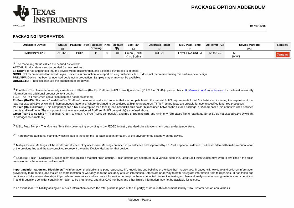
PACKAGING INFORMATION
Orderable Device Status(1)
Package Type PackageDrawing
Pins PackageQty
Eco Plan(2)
Lead/Ball Finish(6)
MSL Peak Temp(3)
Op Temp (°C) Device Marking(4/5)
Samples
LM1949N/NOPB ACTIVE PDIP P 8 40 Green (RoHS& no Sb/Br)
CU SN Level-1-NA-UNLIM -55 to 125 LM1949N
(1) The marketing status values are defined as follows:ACTIVE: Product device recommended for new designs.LIFEBUY: TI has announced that the device will be discontinued, and a lifetime-buy period is in effect.NRND: Not recommended for new designs. Device is in production to support existing customers, but TI does not recommend using this part in a new design.PREVIEW: Device has been announced but is not in production. Samples may or may not be available.OBSOLETE: TI has discontinued the production of the device.
(2) Eco Plan - The planned eco-friendly classification: Pb-Free (RoHS), Pb-Free (RoHS Exempt), or Green (RoHS & no Sb/Br) - please check http://www.ti.com/productcontent for the latest availabilityinformation and additional product content details.TBD: The Pb-Free/Green conversion plan has not been defined.Pb-Free (RoHS): TI's terms "Lead-Free" or "Pb-Free" mean semiconductor products that are compatible with the current RoHS requirements for all 6 substances, including the requirement thatlead not exceed 0.1% by weight in homogeneous materials. Where designed to be soldered at high temperatures, TI Pb-Free products are suitable for use in specified lead-free processes.Pb-Free (RoHS Exempt): This component has a RoHS exemption for either 1) lead-based flip-chip solder bumps used between the die and package, or 2) lead-based die adhesive used betweenthe die and leadframe. The component is otherwise considered Pb-Free (RoHS compatible) as defined above.Green (RoHS & no Sb/Br): TI defines "Green" to mean Pb-Free (RoHS compatible), and free of Bromine (Br) and Antimony (Sb) based flame retardants (Br or Sb do not exceed 0.1% by weightin homogeneous material)
(3) MSL, Peak Temp. - The Moisture Sensitivity Level rating according to the JEDEC industry standard classifications, and peak solder temperature.
(4) There may be additional marking, which relates to the logo, the lot trace code information, or the environmental category on the device.
(5) Multiple Device Markings will be inside parentheses. Only one Device Marking contained in parentheses and separated by a "~" will appear on a device. If a line is indented then it is a continuationof the previous line and the two combined represent the entire Device Marking for that device.
(6) Lead/Ball Finish - Orderable Devices may have multiple material finish options. Finish options are separated by a vertical ruled line. Lead/Ball Finish values may wrap to two lines if the finishvalue exceeds the maximum column width.
Important Information and Disclaimer:The information provided on this page represents TI's knowledge and belief as of the date that it is provided. TI bases its knowledge and belief on informationprovided by third parties, and makes no representation or warranty as to the accuracy of such information. Efforts are underway to better integrate information from third parties. TI has taken andcontinues to take reasonable steps to provide representative and accurate information but may not have conducted destructive testing or chemical analysis on incoming materials and chemicals.TI and TI suppliers consider certain information to be proprietary, and thus CAS numbers and other limited information may not be available for release.
In no event shall TI's liability arising out of such information exceed the total purchase price of the TI part(s) at issue in this document sold by TI to Customer on an annual basis.
PACKAGE OPTION ADDENDUM
www.ti.com 19-Mar-2015
Addendum-Page 2
IMPORTANT NOTICE
Texas Instruments Incorporated and its subsidiaries (TI) reserve the right to make corrections, enhancements, improvements and otherchanges to its semiconductor products and services per JESD46, latest issue, and to discontinue any product or service per JESD48, latestissue. Buyers should obtain the latest relevant information before placing orders and should verify that such information is current andcomplete. All semiconductor products (also referred to herein as “components”) are sold subject to TI’s terms and conditions of salesupplied at the time of order acknowledgment.TI warrants performance of its components to the specifications applicable at the time of sale, in accordance with the warranty in TI’s termsand conditions of sale of semiconductor products. Testing and other quality control techniques are used to the extent TI deems necessaryto support this warranty. Except where mandated by applicable law, testing of all parameters of each component is not necessarilyperformed.TI assumes no liability for applications assistance or the design of Buyers’ products. Buyers are responsible for their products andapplications using TI components. To minimize the risks associated with Buyers’ products and applications, Buyers should provideadequate design and operating safeguards.TI does not warrant or represent that any license, either express or implied, is granted under any patent right, copyright, mask work right, orother intellectual property right relating to any combination, machine, or process in which TI components or services are used. Informationpublished by TI regarding third-party products or services does not constitute a license to use such products or services or a warranty orendorsement thereof. Use of such information may require a license from a third party under the patents or other intellectual property of thethird party, or a license from TI under the patents or other intellectual property of TI.Reproduction of significant portions of TI information in TI data books or data sheets is permissible only if reproduction is without alterationand is accompanied by all associated warranties, conditions, limitations, and notices. TI is not responsible or liable for such altereddocumentation. Information of third parties may be subject to additional restrictions.Resale of TI components or services with statements different from or beyond the parameters stated by TI for that component or servicevoids all express and any implied warranties for the associated TI component or service and is an unfair and deceptive business practice.TI is not responsible or liable for any such statements.Buyer acknowledges and agrees that it is solely responsible for compliance with all legal, regulatory and safety-related requirementsconcerning its products, and any use of TI components in its applications, notwithstanding any applications-related information or supportthat may be provided by TI. Buyer represents and agrees that it has all the necessary expertise to create and implement safeguards whichanticipate dangerous consequences of failures, monitor failures and their consequences, lessen the likelihood of failures that might causeharm and take appropriate remedial actions. Buyer will fully indemnify TI and its representatives against any damages arising out of the useof any TI components in safety-critical applications.In some cases, TI components may be promoted specifically to facilitate safety-related applications. With such components, TI’s goal is tohelp enable customers to design and create their own end-product solutions that meet applicable functional safety standards andrequirements. Nonetheless, such components are subject to these terms.No TI components are authorized for use in FDA Class III (or similar life-critical medical equipment) unless authorized officers of the partieshave executed a special agreement specifically governing such use.Only those TI components which TI has specifically designated as military grade or “enhanced plastic” are designed and intended for use inmilitary/aerospace applications or environments. Buyer acknowledges and agrees that any military or aerospace use of TI componentswhich have not been so designated is solely at the Buyer's risk, and that Buyer is solely responsible for compliance with all legal andregulatory requirements in connection with such use.TI has specifically designated certain components as meeting ISO/TS16949 requirements, mainly for automotive use. In any case of use ofnon-designated products, TI will not be responsible for any failure to meet ISO/TS16949.
Products ApplicationsAudio www.ti.com/audio Automotive and Transportation www.ti.com/automotiveAmplifiers amplifier.ti.com Communications and Telecom www.ti.com/communicationsData Converters dataconverter.ti.com Computers and Peripherals www.ti.com/computersDLP® Products www.dlp.com Consumer Electronics www.ti.com/consumer-appsDSP dsp.ti.com Energy and Lighting www.ti.com/energyClocks and Timers www.ti.com/clocks Industrial www.ti.com/industrialInterface interface.ti.com Medical www.ti.com/medicalLogic logic.ti.com Security www.ti.com/securityPower Mgmt power.ti.com Space, Avionics and Defense www.ti.com/space-avionics-defenseMicrocontrollers microcontroller.ti.com Video and Imaging www.ti.com/videoRFID www.ti-rfid.comOMAP Applications Processors www.ti.com/omap TI E2E Community e2e.ti.comWireless Connectivity www.ti.com/wirelessconnectivity
Mailing Address: Texas Instruments, Post Office Box 655303, Dallas, Texas 75265Copyright © 2016, Texas Instruments Incorporated