Lithographically fabricated optical cavities for ... · Lithographically fabricated optical...
7
Lithographically fabricated optical cavities for refractive index sensing Mark Adams, Guy A. DeRose, Marko Loncar, and Axel Scherer Citation: Journal of Vacuum Science & Technology B 23, 3168 (2005); doi: 10.1116/1.2127945 View online: http://dx.doi.org/10.1116/1.2127945 View Table of Contents: http://scitation.aip.org/content/avs/journal/jvstb/23/6?ver=pdfcov Published by the AVS: Science & Technology of Materials, Interfaces, and Processing Articles you may be interested in Enhancing outcoupling efficiency of indium-tin-oxide-free organic light-emitting diodes via nanostructured high index layers Appl. Phys. Lett. 96, 243302 (2010); 10.1063/1.3455098 Edge emitting quantum cascade microlasers on InP with deeply etched one-dimensional photonic crystals Appl. Phys. Lett. 91, 071104 (2007); 10.1063/1.2771054 Cladding mode resonances of etch-eroded fiber Bragg grating for ambient refractive index sensing Appl. Phys. Lett. 88, 133902 (2006); 10.1063/1.2191951 High refractive-index microspheres of optical cavity structure Appl. Phys. Lett. 82, 3173 (2003); 10.1063/1.1573331 Etching depth dependence of the effective refractive index in two-dimensional photonic-crystal-patterned vertical- cavity surface-emitting laser structures Appl. Phys. Lett. 82, 1344 (2003); 10.1063/1.1556562 Redistribution subject to AVS license or copyright; see http://scitation.aip.org/termsconditions. Download to IP: 140.247.173.34 On: Thu, 07 Jan 2016 02:21:38
Transcript of Lithographically fabricated optical cavities for ... · Lithographically fabricated optical...
Lithographically fabricated optical cavities for refractive index sensingMark Adams, Guy A. DeRose, Marko Loncar, and Axel Scherer Citation: Journal of Vacuum Science & Technology B 23, 3168 (2005); doi: 10.1116/1.2127945 View online: http://dx.doi.org/10.1116/1.2127945 View Table of Contents: http://scitation.aip.org/content/avs/journal/jvstb/23/6?ver=pdfcov Published by the AVS: Science & Technology of Materials, Interfaces, and Processing Articles you may be interested in Enhancing outcoupling efficiency of indium-tin-oxide-free organic light-emitting diodes via nanostructured highindex layers Appl. Phys. Lett. 96, 243302 (2010); 10.1063/1.3455098 Edge emitting quantum cascade microlasers on InP with deeply etched one-dimensional photonic crystals Appl. Phys. Lett. 91, 071104 (2007); 10.1063/1.2771054 Cladding mode resonances of etch-eroded fiber Bragg grating for ambient refractive index sensing Appl. Phys. Lett. 88, 133902 (2006); 10.1063/1.2191951 High refractive-index microspheres of optical cavity structure Appl. Phys. Lett. 82, 3173 (2003); 10.1063/1.1573331 Etching depth dependence of the effective refractive index in two-dimensional photonic-crystal-patterned vertical-cavity surface-emitting laser structures Appl. Phys. Lett. 82, 1344 (2003); 10.1063/1.1556562
Redistribution subject to AVS license or copyright; see http://scitation.aip.org/termsconditions. Download to IP: 140.247.173.34 On: Thu, 07 Jan 2016 02:21:38
Lithographically fabricated optical cavities for refractive index sensingMark AdamsENSCO Inc., 4849 North Wickham Road, Melbourne, Florida 32940
Guy A. DeRosea�
Elcetrical Engineering and Applied Physics Department, California Institute of Technology,1200 East California Boulevard, Pasadena, California 91125
Marko LoncarDivision of Engineering and Applied Science, Harvard University, 9 Oxford Street,Cambridge, Massachusetts 02138
Axel SchererElectrical Engineering and Applied Physics Department, California Institute of Technology,1200 East California Boulevard, Pasadena, California 91125
�Received 3 June 2005; accepted 26 September 2005; published 7 December 2005�
Since the development of distributed Bragg gratings, high resolution lithography and etching havebeen applied towards the concentration of light. The most important application of lithographicallyfabricated microcavities has been for the spectral control over laser emission. Here we describe theopportunities that arise from further miniaturization of laser cavities by using high index contrastphotonic crystal mirrors and annular Bragg reflectors. We have used these optical cavities, withmode volumes as small as 10−17 l, to perform spectroscopic analysis and compare the mode volumesand sensitivities of these geometries. © 2005 American Vacuum Society. �DOI: 10.1116/1.2127945�
I. INTRODUCTION
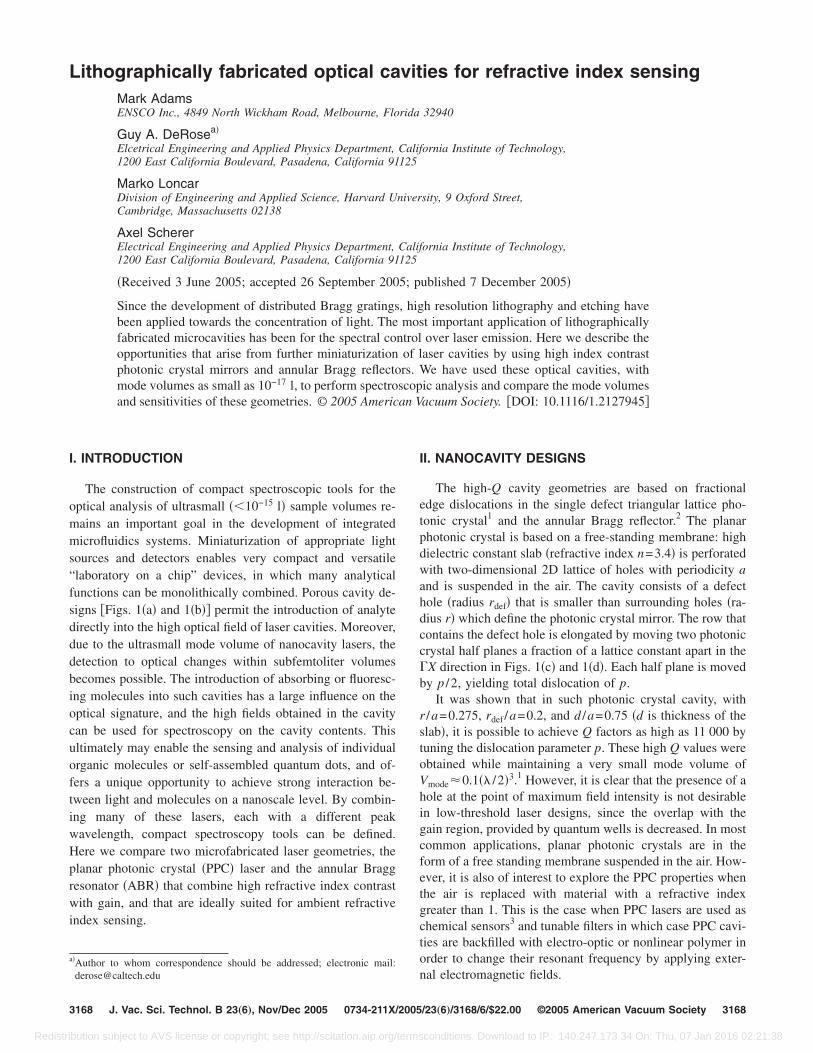
The construction of compact spectroscopic tools for theoptical analysis of ultrasmall ��10−15 l� sample volumes re-mains an important goal in the development of integratedmicrofluidics systems. Miniaturization of appropriate lightsources and detectors enables very compact and versatile“laboratory on a chip” devices, in which many analyticalfunctions can be monolithically combined. Porous cavity de-signs �Figs. 1�a� and 1�b�� permit the introduction of analytedirectly into the high optical field of laser cavities. Moreover,due to the ultrasmall mode volume of nanocavity lasers, thedetection to optical changes within subfemtoliter volumesbecomes possible. The introduction of absorbing or fluoresc-ing molecules into such cavities has a large influence on theoptical signature, and the high fields obtained in the cavitycan be used for spectroscopy on the cavity contents. Thisultimately may enable the sensing and analysis of individualorganic molecules or self-assembled quantum dots, and of-fers a unique opportunity to achieve strong interaction be-tween light and molecules on a nanoscale level. By combin-ing many of these lasers, each with a different peakwavelength, compact spectroscopy tools can be defined.Here we compare two microfabricated laser geometries, theplanar photonic crystal �PPC� laser and the annular Braggresonator �ABR� that combine high refractive index contrastwith gain, and that are ideally suited for ambient refractiveindex sensing.
II. NANOCAVITY DESIGNS
The high-Q cavity geometries are based on fractionaledge dislocations in the single defect triangular lattice pho-tonic crystal1 and the annular Bragg reflector.2 The planarphotonic crystal is based on a free-standing membrane: highdielectric constant slab �refractive index n=3.4� is perforatedwith two-dimensional 2D lattice of holes with periodicity aand is suspended in the air. The cavity consists of a defecthole �radius rdef� that is smaller than surrounding holes �ra-dius r� which define the photonic crystal mirror. The row thatcontains the defect hole is elongated by moving two photoniccrystal half planes a fraction of a lattice constant apart in the�X direction in Figs. 1�c� and 1�d�. Each half plane is movedby p /2, yielding total dislocation of p.
It was shown that in such photonic crystal cavity, withr /a=0.275, rdef /a=0.2, and d /a=0.75 �d is thickness of theslab�, it is possible to achieve Q factors as high as 11 000 bytuning the dislocation parameter p. These high Q values wereobtained while maintaining a very small mode volume ofVmode�0.1�� /2�3.1 However, it is clear that the presence of ahole at the point of maximum field intensity is not desirablein low-threshold laser designs, since the overlap with thegain region, provided by quantum wells is decreased. In mostcommon applications, planar photonic crystals are in theform of a free standing membrane suspended in the air. How-ever, it is also of interest to explore the PPC properties whenthe air is replaced with material with a refractive indexgreater than 1. This is the case when PPC lasers are used aschemical sensors3 and tunable filters in which case PPC cavi-ties are backfilled with electro-optic or nonlinear polymer inorder to change their resonant frequency by applying exter-nal electromagnetic fields.
a�Author to whom correspondence should be addressed; electronic mail:[email protected]
3168 3168J. Vac. Sci. Technol. B 23„6…, Nov/Dec 2005 0734-211X/2005/23„6…/3168/6/$22.00 ©2005 American Vacuum Society
Redistribution subject to AVS license or copyright; see http://scitation.aip.org/termsconditions. Download to IP: 140.247.173.34 On: Thu, 07 Jan 2016 02:21:38
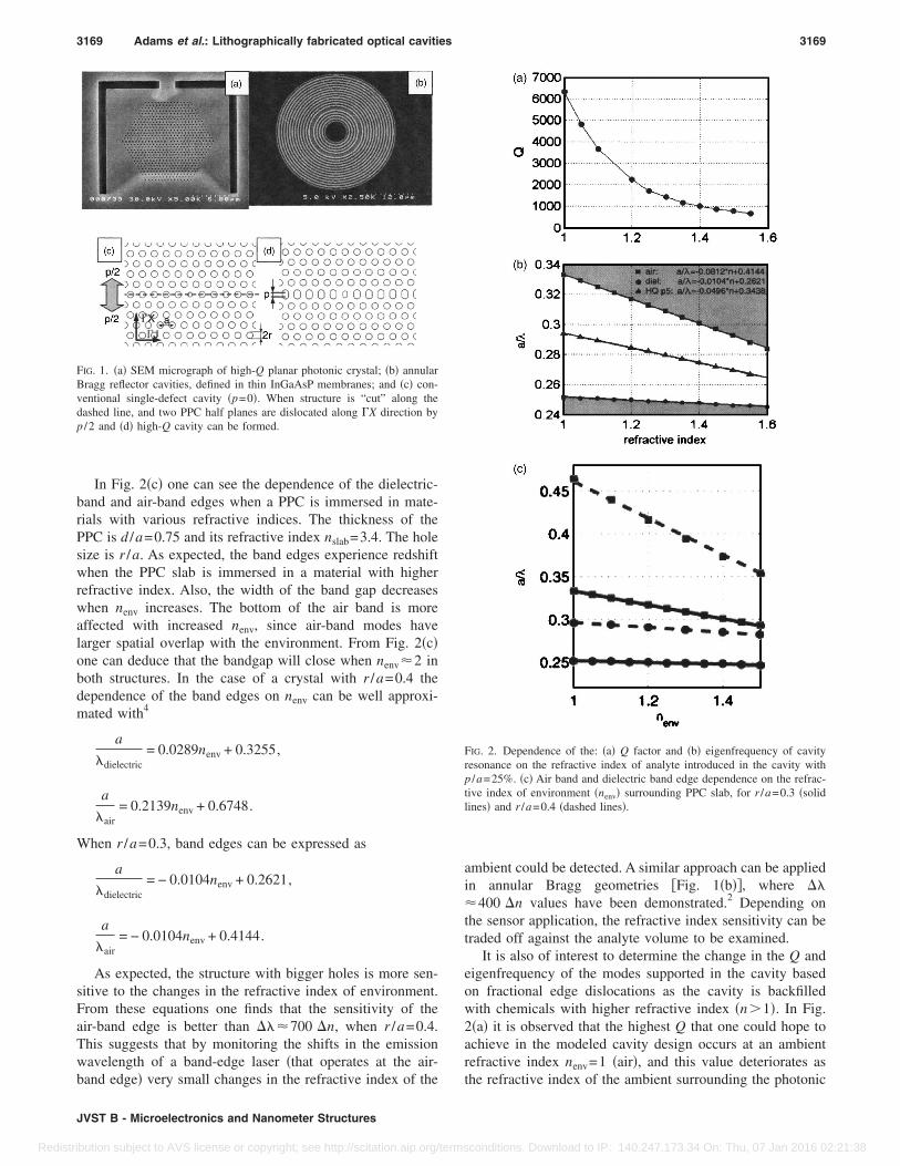
In Fig. 2�c� one can see the dependence of the dielectric-band and air-band edges when a PPC is immersed in mate-rials with various refractive indices. The thickness of thePPC is d /a=0.75 and its refractive index nslab=3.4. The holesize is r /a. As expected, the band edges experience redshiftwhen the PPC slab is immersed in a material with higherrefractive index. Also, the width of the band gap decreaseswhen nenv increases. The bottom of the air band is moreaffected with increased nenv, since air-band modes havelarger spatial overlap with the environment. From Fig. 2�c�one can deduce that the bandgap will close when nenv�2 inboth structures. In the case of a crystal with r /a=0.4 thedependence of the band edges on nenv can be well approxi-mated with4
a
�dielectric= 0.0289nenv + 0.3255,
a
�air= 0.2139nenv + 0.6748.
When r /a=0.3, band edges can be expressed as
a
�dielectric= − 0.0104nenv + 0.2621,
a
�air= − 0.0104nenv + 0.4144.
As expected, the structure with bigger holes is more sen-sitive to the changes in the refractive index of environment.From these equations one finds that the sensitivity of theair-band edge is better than ���700 �n, when r /a=0.4.This suggests that by monitoring the shifts in the emissionwavelength of a band-edge laser �that operates at the air-band edge� very small changes in the refractive index of the
ambient could be detected. A similar approach can be appliedin annular Bragg geometries �Fig. 1�b��, where ���400 �n values have been demonstrated.2 Depending onthe sensor application, the refractive index sensitivity can betraded off against the analyte volume to be examined.
It is also of interest to determine the change in the Q andeigenfrequency of the modes supported in the cavity basedon fractional edge dislocations as the cavity is backfilledwith chemicals with higher refractive index �n�1�. In Fig.2�a� it is observed that the highest Q that one could hope toachieve in the modeled cavity design occurs at an ambientrefractive index nenv=1 �air�, and this value deteriorates asthe refractive index of the ambient surrounding the photonic
FIG. 1. �a� SEM micrograph of high-Q planar photonic crystal; �b� annularBragg reflector cavities, defined in thin InGaAsP membranes; and �c� con-ventional single-defect cavity �p=0�. When structure is “cut” along thedashed line, and two PPC half planes are dislocated along �X direction byp /2 and �d� high-Q cavity can be formed.
FIG. 2. Dependence of the: �a� Q factor and �b� eigenfrequency of cavityresonance on the refractive index of analyte introduced in the cavity withp /a=25%. �c� Air band and dielectric band edge dependence on the refrac-tive index of environment �nenv� surrounding PPC slab, for r /a=0.3 �solidlines� and r /a=0.4 �dashed lines�.
3169 Adams et al.: Lithographically fabricated optical cavities 3169
JVST B - Microelectronics and Nanometer Structures
Redistribution subject to AVS license or copyright; see http://scitation.aip.org/termsconditions. Download to IP: 140.247.173.34 On: Thu, 07 Jan 2016 02:21:38
crystal cavity is increased. This decrease in Q is a result ofthe weaker vertical confinement of light by total internal re-flection, and can be compensated for by increasing the thick-ness of the photonic crystal slab.
It is interesting to note that the frequency of the resonantmode also depends linearly on the refractive index of theenvironment �nenv� �Fig. 2�b��. From linear fits of the depen-dence of the resonant frequency on nenv, one can estimate thesensitivity of the cavity, and find that the wavelength shift ofthe resonance is approximately ���266 �nenv, where �nenv
is the change in refractive index. The simplest method ofoptically sensing ambient material uses wavelength shifts inthe laser spectrum when the laser is immersed into a solutionor exposed to a material to measure its refractive index. Inthis method, the sensitivity of the sensor depends on thesmallest change in refractive index that can be optically de-tected. In passive devices, this is related to the width of thecavity resonance peak, which in turn is determined by cavityquality Q. If one assumes that the cavity is embedded in atypical polymer �nenv=1.4� a wavelength shift that is stillobservable from cavity with Q=1000 is ��=1.55 nm, whichcorresponds to change in refractive index of �n�0.0056. Onthe other hand, once optical gain is introduced into the cavitythe linewidth of emission is significantly narrowed ����0.12 nm�, and sensitivities to �n�0.001 can be measuredeven in cavities with modest Q factors. Figures 2�a� and 2�b�suggest that the edge of the air band is even more sensitive tochanges in the refractive index than the cavity mode itself.Therefore, band-edge lasers5–8 and ABR lasers2 might beeven better choice for applications where high sensitivity tothe changes of refractive index are needed. However, band-edge lasers operate at extended bulk PPC modes, with largemode volumes, and therefore are not suitable for applicationswhere high spatial sensitivity is needed �e.g., in single-molecule detection�.
The field strength in the central defect hole of the cavitycan also be estimated. The energy stored in the resonator canbe written as
Wstored = PQenv�
2�c,
where Qenv is the Q factor of the cavity immersed in theenvironment with refractive index nenv. Normalized energyof the cavity mode �Kenv� can be written as
Kenv =��� 1
2��E�2 + 12��H�2dV
�def�Edef�2� �2 �3 =
Wstored
�env�0�Edef�2� �2 �3
and depends on the environment that the cavity is immersedinto. The Edef is the maximum electric field strength in thehole at the center of the cavity. It is important to rememberthat the resonator can be embedded in materials differentfrom air, and therefore one has to use appropriate permeabil-ity of the material for �def. Combining these equations, themaximum field strength at the center of the cavity can beexpressed as
Edef = � 4
�nenv P
4��0cQenv
Kenv.
From calculations of the dependence of Edef on refractiveindex of the environment nenv, we predict that the maximumfield is on the order of the breakdown strength of air, orEbreakdown=3V /�m.
III. FABRICATION PROCEDURE
InGaAsP quantum well material was grown on InP sub-strate using metalorganic chemical vapor deposition. Opticalgain was provided by four 9 nm thick, compressivelystrained, quantum wells with an electronic band gap at �bg
=1.55 �m, separated by 20 nm thick InGaAsP barriers ��bg
=1.22 �m�. This active material was placed in the center ofa 330 nm thick InGaAsP slab ��bg=1.22 �m�, with a 1 �mthick sacrificial InP layer underneath the slab. An InGaAsetch stop was introduced above the InP substrate, and theactive quaternary material was designed to operate at�=1.55 �m. The fabrication procedure consisted ofelectron-beam lithography, followed by two dry- and onewet-etching steps. The etch mask consists of 100–140 nmthick SiO2 or Si3N4 layer, deposited at room temperatureusing a rf sputtering technique. Both masks performed simi-larly in the etching chemistry, but in this section a Si3N4
layer was used as the dielectric mask layer. 120 nm of poly-�methyl methacrylate� �PMMA�, electron-beam �e-beam�sensitive resist, was deposited on top of the Si3N4 masklayer. A 2% solution of PMMA �molecular weight 950 K�diluted in chlorobenzene was used. The PMMA was bakedon a hot plate at 150 °C for 40 min. e-beam lithography wasperformed using a Leica EBPG 5000+ operating at 100 keV,and the dose used to define the patterns in PMMA was500 �C/cm2. By varying the electron dose, one can span theentire design space of the PPC and ABR nanocavities. Uponcompleting e-beam lithography, the PMMA was developedin 1:3 methyl isobutyl ketone: isopropyl alcohol �IPA�PMMA developer and rinsed for 15 s in IPA. The PMMApatterns were transferred into the Si3N4 layer using reactiveion etching �RIE�. 20 sccm of CHF3 reactive gas was usedand the chamber pressure was kept at 16 mTorr. The rf powerused in this RIE step was 90 W and with a dc bias of 480 Vfor 3 min. At the end, the patterns were transferred throughthe InGaAsP active layer into the InP substrate with aninductive-coupled RIE using an HI/H2 plasma chemistry.9
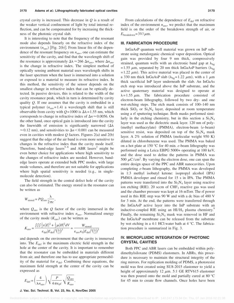
Finally, the remaining Si3N4 mask was removed in HF andthe InGaAsP membrane can be released from the substrateby wet etching in a 4:1 HCl:water bath at 4 °C. The fabrica-tion procedure is summarized in Fig. 3.
IV. MICROFLUIDIC INTEGRATION OF PHOTONICCRYSTAL CAVITIES
Both PPC and ABR lasers can be embedded within poly-dimethylsiloxane �PDMS� elastomers. In ABRs, this proce-dure is necessary to maintain the structural integrity of thering mirrors. For replication molding of PDMS, a photoresistmold was first created using SU8-2015 elastomer to yield aheight of approximately 12 �m. 5:1 GE RTV615 elastomerwas then poured onto the mold and partially cured at 80 °Cfor 45 min to create flow channels. Once holes have been
3170 Adams et al.: Lithographically fabricated optical cavities 3170
J. Vac. Sci. Technol. B, Vol. 23, No. 6, Nov/Dec 2005
Redistribution subject to AVS license or copyright; see http://scitation.aip.org/termsconditions. Download to IP: 140.247.173.34 On: Thu, 07 Jan 2016 02:21:38
punched to access these flow channels, the flow layer can bealigned onto the laser sensor chip so that one flow channelpasses over several nanolaser cavities. In order to embed thePPC structure, it must first be coated with PMMA since thatpolymer does not interfere with the PDMS curing procedure.After baking, the assembly was allowed to cool to roomtemperature and then a layer of PMMA was spun on top ofthe assembly to cover the backside of the InP chip.
20:1 GE RTV615 was poured onto the InP wafer assem-bly and cured. Once the PDMS was fully cured, the assem-bly was placed into acetone at 95 °C until the laser structurehad lifted off the silicon wafer. Since PDMS is permeable,the acetone seeps through the PDMS layer and dissolves thePMMA that has bonded the laser sources to the silicon wafer.After the two have been separated, the acetone was removedand replaced with IPA. When the laser is freed from thesilicon wafer, it is still encapsulated by the PDMS. ThePDMS can then be removed from the silicon wafer with the
PPC devices and placed onto a hotplate at 200 °C to drive offany remaining solvents which may be trapped inside thePDMS.
In order to seal the flow layer to the laser layer, it isnecessary to plasma treat the surface of the laser PDMSlayer. The PDMS layer was etched with a combination of O2
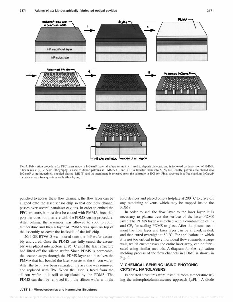
and CF4 for sealing PDMS to glass. After the plasma treat-ment the flow layer and laser layer can be aligned, sealed,and then cured overnight at 80 °C. For applications in whichit is not too critical to have individual flow channels, a largewell, which encompasses the entire laser array, can be fabri-cated using similar methods. A diagram for the replicationmolding process of the flow channels in PDMS is shown inFig. 4.
V. CHEMICAL SENSING USING PHOTONICCRYSTAL NANOLASERS
Fabricated structures were tested at room temperature us-ing the microphotoluminescence approach ��PL�. A diode
FIG. 3. Fabrication procedure for PPC lasers made in InGaAsP material. rf sputtering �1� is used to deposit dielectric and is followed by deposition of PMMAe-beam resist �2�. e-beam lithography is used to define patterns in PMMA �3� and RIE to transfer them into Si3N4 �4�. Finally, patterns are etched intoInGaAsP using inductively coupled plasma–RIE �5� and the membrane is released from the substrate in HCl �6�. Final structure is a free standing InGaAsPmembrane with four quantum wells �thin layers�.
3171 Adams et al.: Lithographically fabricated optical cavities 3171
JVST B - Microelectronics and Nanometer Structures
Redistribution subject to AVS license or copyright; see http://scitation.aip.org/termsconditions. Download to IP: 140.247.173.34 On: Thu, 07 Jan 2016 02:21:38
laser emitting at �=830 nm was used to pump the lasers with�1% duty cycles, i.e., 15–30 ns pulses with 3 �s periodicity.The pump beam was focused through a 100 objective lensonto the sample surface to obtain a spot size of about 3 �m.The emission from the cavities was collected through thesame lens, and the spectrum of the emitted signal was ana-lyzed with an optical spectrum analyzer. In order to explorethe sensitivity of the lasers on the changes in the refractiveindex of the environment, fluids with known refractive indexin the range nenv·�1.295,1.335� �specified at �=1.5 �m� withstep �nenv=0.005 were used.
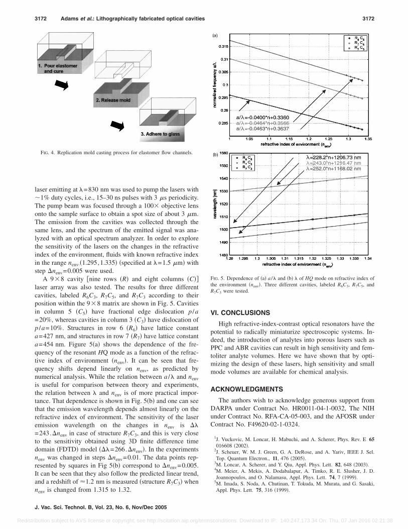
A 98 cavity �nine rows �R� and eight columns �C��laser array was also tested. The results for three differentcavities, labeled R6C3, R7C5, and R7C3 according to theirposition within the 98 matrix are shown in Fig. 5. Cavitiesin column 5 �C5� have fractional edge dislocation p /a=20%, whereas cavities in column 3 �C3� have dislocation ofp /a=10%. Structures in row 6 �R6� have lattice constanta=427 nm, and structures in row 7 �R7� have lattice constanta=454 nm. Figure 5�a� shows the dependence of the fre-quency of the resonant HQ mode as a function of the refrac-tive index of environment �nenv�. It can be seen that fre-quency shifts depend linearly on nenv, as predicted bynumerical analysis. While the relation between a /� and nenv
is useful for comparison between theory and experiments,the relation between � and nenv is of more practical impor-tance. That dependence is shown in Fig. 5�b� and one can seethat the emission wavelength depends almost linearly on therefractive index of environment. The sensitivity of the laseremission wavelength on the changes in nenv is ��=243.�nenv in case of structure R7C3, and this is very closeto the sensitivity obtained using 3D finite difference timedomain �FDTD� model ���=266.�nenv�. In the experimentsnenv was changed in steps �nenv=0.01. The data points rep-resented by squares in Fig 5�b� correspond to �nenv=0.005.It can be seen that they also follow the predicted linear trend,and a redshift of �1.2 nm is measured �structure R7C3� whennenv is changed from 1.315 to 1.32.
VI. CONCLUSIONS
High refractive-index-contrast optical resonators have thepotential to radically miniaturize spectroscopic systems. In-deed, the introduction of analytes into porous lasers such asPPC and ABR cavities can result in high sensitivity and fem-toliter analyte volumes. Here we have shown that by opti-mizing the design of these lasers, high sensitivity and smallmode volumes are available for chemical analysis.
ACKNOWLEDGMENTS
The authors wish to acknowledge generous support fromDARPA under Contract No. HR0011-04-1-0032, The NIHunder Contract No. RFA-CA-05-003, and the AFOSR underContract No. F49620-02-1-0324.
1J. Vuckovic, M. Loncar, H. Mabuchi, and A. Scherer, Phys. Rev. E 65016608 �2002�.
2J. Scheuer, W. M. J. Green, G. A. DeRose, and A. Yariv, IEEE J. Sel.Top. Quantum Electron., 11, 476 �2005�.
3M. Loncar, A. Scherer, and Y. Qiu, Appl. Phys. Lett. 82, 648 �2003�.4M. Meier, A. Mekis, A. Dodabalapur, A. Timko, R. E. Slusher, J. D.Joannopoulos, and O. Nalamasu, Appl. Phys. Lett. 74, 7 �1999�.
5M. Imada, S. Noda, A. Chutinan, T. Tokuda, M. Murata, and G. Sasaki,Appl. Phys. Lett. 75, 316 �1999�.
FIG. 4. Replication mold casting process for elastomer flow channels.
FIG. 5. Dependence of �a� a /� and �b� � of HQ mode on refractive index ofthe environment �nenv�. Three different cavities, labeled R6C3, R7C5, andR7C3 were tested.
3172 Adams et al.: Lithographically fabricated optical cavities 3172
J. Vac. Sci. Technol. B, Vol. 23, No. 6, Nov/Dec 2005
Redistribution subject to AVS license or copyright; see http://scitation.aip.org/termsconditions. Download to IP: 140.247.173.34 On: Thu, 07 Jan 2016 02:21:38

6M. Notomi, H. Suzuki, and T. Tamamura, Appl. Phys. Lett. 78, 1325�2001�.
7H. Ryu, S. H. Kwon, Y. J. Lee, Y. H. Lee, and J. S. Kim, Appl. Phys. Lett.80, 3476 �2002�.
8S. Noda, M. Yokoyama, M. Imada, A. Chutinan, and M. Mochizuki,Science 293, 1123 �2001�.
9M. Loncar, M. Hochberg, A. Scherer, and Y. M. Qiu, Opt. Lett. 29, 721�2004�.
3173 Adams et al.: Lithographically fabricated optical cavities 3173
JVST B - Microelectronics and Nanometer Structures
Redistribution subject to AVS license or copyright; see http://scitation.aip.org/termsconditions. Download to IP: 140.247.173.34 On: Thu, 07 Jan 2016 02:21:38