Linde Material Handling Linde Material Handling Division Linde Hydraulics and.
26 WWW.SILICONSEMICONDUCTOR.NET l ISSUE 1 2017 l COPYRIGHT SILICON SEMICONDUCTOR
manufacturing hydrogen
Hydrogen in Electronics: Growing applications and consumptionHydrogen will play an increasing role in semiconductor manufacturing due to its wide serviceability and importance in extreme ultraviolet (EUV) lithography. Linde Electronics’ head of market development, Dr. Paul Stockman, explains why ensuring a safe and reliable source of hydrogen will be critical for next-generation device manufacturers.
COLORLESS, odorless, and even burning with an invisible flame, hydrogen is nevertheless omnipresent in the semiconductor fab and an increasingly important material for chip manufacturing. Leading-edge wafers consume more than their own weight of this ultra-light gas during processing and the long-anticipated adoption of EUV (extreme ultra-violet) lithography will drive demand even further.
This article reviews the properties of hydrogen that make it essential for leading-edge semiconductor manufacturing, details the specific processes that require hydrogen including the coming high-demand EUV application, and reviews the different supply options available.
Important properties of hydrogenComposed of the lightest element, molecular hydrogen (H2) has some extreme properties that give rise to its usefulness and hazards.
Chemical reducer: Molecular hydrogen is useful for the direct substitution of hydrogen atoms for other elements, as well as influencing the pathways of key chemical reactions.
Heat transfer: Hydrogen is able to convectively remove heat faster than any molecule other than helium.
Light mass: Hydrogen is one of the smallest molecular compounds of any gas or liquid fluid and can therefore “fit” in places that other molecules cannot, including in the porous voids of some solid materials. Its light mass also makes it relatively inexpensive to transport on a volume basis, but conversely expensive to transport on a mass basis. Compared to air, hydrogen is nearly 15 times lighter and quickly rises and diffuses.
Kinetic isotope effect: Chemical reaction rates change when one stable isotope of an atom is changed for another. Often this is a slight effect, but because hydrogen’s (mass = 1 amu) stable isotope deuterium (mass = 2 amu) is twice as heavy, this effect can be significant.
Low boiling point: Hydrogen boils at a very low 20.7 K (-423.2°F or -252.9°C), second only to helium. It therefore takes a lot of energy to liquefy hydrogen, a consideration in its transport and purification.

COPYRIGHT SILICON SEMICONDUCTOR l ISSUE 1 2017 l WWW.SILICONSEMICONDUCTOR.NET 27
manufacturing hydrogen
Flammable and explosive limits: Hydrogen’s most hazardous properties are its wide range for flammability (ability to burn with an ignition source) and explosivity (ability to explode or to cause a shock wave) in air. Hydrogen forms flammable mixtures between 4 and 75% concentration in air, and explosive mixtures between 18 and 59% in air. Fortunately, the buoyancy of hydrogen relative to air means small leaks of hydrogen usually diffuse rapidly below these limits.
Existing process applicationsHydrogen has been adopted as a material in processes throughout the fab. Its unique chemical properties continue to expand its usefulness. These applications typically use flows of 100s to 1,000s of sccm (standard cubic centimetre per minute):
Epitaxy: Hydrogen is used as a reducing agent during the epitaxial growth of crystalline thin-films. This is often used to make a starting silicon surface for semiconductor manufacturing by reacting newly cut and polished silicon wafers with trichlorosilane (SiHCl3) in an epi-house or end-user fab. The hydrogen reduces the gas-phase chlorine atoms, and the HCl product is removed from the reactor as a gas. Leading-edge channel materials like strained silicon,
silicon-germanium, and germanium are also grown using hydrogen-mediated epitaxy.
Deposition: Hydrogen can also be incorporated directly into thin-films to disrupt crystal lattices to make them less crystalline, more amorphous. This is often used with silicon thin-films, which need to be made more electrically insulating.
Plasma etch: Hydrogen and hydrogen-containing plasmas are used to directly react with the surface of the wafer in order to clean or remove unwanted thin films, especially for removing unwanted fluorocarbon deposits on silicon oxides.
Anneal: Silicon wafers are heated to temperatures over 1000°C, often at elevated pressure, in order to repair their crystal structures. Hydrogen assists by transferring heat uniformly over the surface of the wafer, and also by penetrating into the crystal lattice to react with atomic impurities.
Passivation: Hydrogen is used to react and remove native oxides on silicon surfaces and to mediate the reconstruction of silicon-silicon bonds in the final layers of the crystal.
28 WWW.SILICONSEMICONDUCTOR.NET l ISSUE 1 2017 l COPYRIGHT SILICON SEMICONDUCTOR
manufacturing hydrogen
Ion implantation: With more precision than bulk annealing and passivation, protons produced from hydrogen gas can be implanted to specific depths and concentrations in a thin film using ion implanters. Not only can hydrogen atoms be inserted to modify a thin film, but in higher doses and implantation energies, it can be used to cleave slivers of silicon and sapphire wafers.
Carrier gas: Hydrogen is used as a carrier gas to entrain (entrap) and transport less volatile chemicals—ordinarily liquids at atmospheric pressure and room temperature—into the reaction chamber. The hydrogen is heated and bubbled through the liquid chemicals. Because the mass of hydrogen is very light compared to entrained chemical vapor, specialized mass flow controllers can then be used to sense, measure, and precisely control the amount of chemical vapor dispensed.
Deuterium defense against hot-carrier injection: Hydrogen bonds to silicon at thin-film interfaces are susceptible to breakage by hot carrier injection, which are electrons and holes caused by short-wavelength radiation like x-rays and gamma rays. In semiconductor structures, deuterium-passivated thin-films have different bond strengths, and a much lower probability of cleavage due to hot carriers.
This is particularly important for chips in critical applications and those in environments with high levels of short-wavelength radiation, like spacecraft. Like regular hydrogen annealing and passivation,
deuterium is reacted with wafers in a pressurized furnace at high temperatures.
Material stabilization: The addition of hydrogen extends the shelf life of important electronic materials like diborane (B2H6) and digermane (Ge2H6), which otherwise slowly decompose. The slightly stronger bonds in deuterated stannane (SnD4) allow it enough stability in a deuterium balance to be useful; the normal isotope version of stannane (SnH4) decomposes too quickly to have commercial applications.
Application for EUVExtreme ultraviolet (EUV) lithography is the much-anticipated new application expected to simplify the process patterning complexity for critical dimensions in leading-edge devices. While it has taken a long time for this technology to come close to commercialization, top-tier manufacturers are coalescing their predictions for volume manufacturing adoption in the 2018-2020 window. Whereas other hydrogen-consuming applications have a usage rate of 100s of sccm, EUV will require much larger flows of 100s of slm (standard liters per minute), or roughly 100 to 1000x more per individual tool.
Deep ultraviolet (DUV) lithography, the current workhorse of the patterning tools, uses an electrical discharge in neon or krypton mixed with halogen gases like fluorine to produce UV light at 193 nm and 248 nm; EUV light production is much more complicated. Tin metal is heated above its melting
COPYRIGHT SILICON SEMICONDUCTOR l ISSUE 1 2017 l WWW.SILICONSEMICONDUCTOR.NET 29
manufacturing hydrogen
point of 232°C, and small droplets of tin (~25 μm diameter) are rapidly (50,000 droplets per second) produced. These droplets are first vaporized and then excited with high-power CO2 lasers. The excited tin atoms emit EUV light at 13.5 nm, which is more than 14 times shorter than the DUV tools.
The light is emitted in all directions and is collected and collimated (aligned) by an array of mirrors. The light is then passed to the primary lithography tool for focusing and image transfer before illuminating the photoresist on the wafer. All materials heavily absorb EUV light. Absorption losses are minimized by using multi-layer reflective optics instead of the transmissive lenses used in DUV lithography, and the entire light source and patterning systems are housed in vacuum chambers. These highly complex tools are expected to cost end users around $100 million USD each, and when fully adopted, a leading-edge fab could require 20 or more of these tools.
Scattered tin debris from the vaporization of droplets is a major potential source of contamination of both the collector and focusing optics. Unmitigated, the lifetimes of these expensive components would be unacceptable. Hydrogen gas is used to shroud the tin excitation region, and tin vapor and aberrant droplets are reacted to form stannane (SnH4), which is then removed from that section of the housing by means of the vacuum line. Higher flows of hydrogen can be used in periodic plasma-based cleaning to remove tin that deposits on the collector optics.
Demand and supplyEven before the adoption of EUV technology, leading-edge logic and foundry processes have begun consuming several normal cubic meters (1000 liters) of hydrogen per wafer processed. This usage trend
is expected to continue increasing in the 10 nm and 7 nm nodes commercialized before widespread EUV use. Consequently, major fabs now use hundreds of Nm3 per hour. EUV, when fully extended to all of the critical layers, will roughly double the amount of hydrogen used in these fabs. In a related application, the largest LED fabs also use hundreds of Nm3 of hydrogen per hour, primarily as a carrier gas and diluent for the gallium, arsine, and phosphorus precursors used to make the light-emitting devices.
Supply of hydrogen to electronics customers has historically been driven by regional source types, engineering and transportation codes, and by end user preferences and process qualification. However, steep demand curves are causing users to consider new supply schemes for access to larger volumes,
Supply of hydrogen to electronics customers has historically been driven by
regional source types, engineering and transportation codes, and by end user preferences and process qualification.
However, steep demand curves are causing users to consider new supply
schemes for access to larger volumes, greater supply chain security, and
lessening of local fab logistics
30 WWW.SILICONSEMICONDUCTOR.NET l ISSUE 1 2017 l COPYRIGHT SILICON SEMICONDUCTOR
manufacturing hydrogen
greater supply chain security, and lessening of local fab logistics.
Over 60 million metric tons of hydrogen are produced globally, almost exclusively from hydrocarbon feedstocks: natural gas, oil, and coal. Most of this is used as a chemical intermediate to make ammonia, methanol, and transportation fuels. Electronics manufacturing consumes much less than 1% of global hydrogen production.
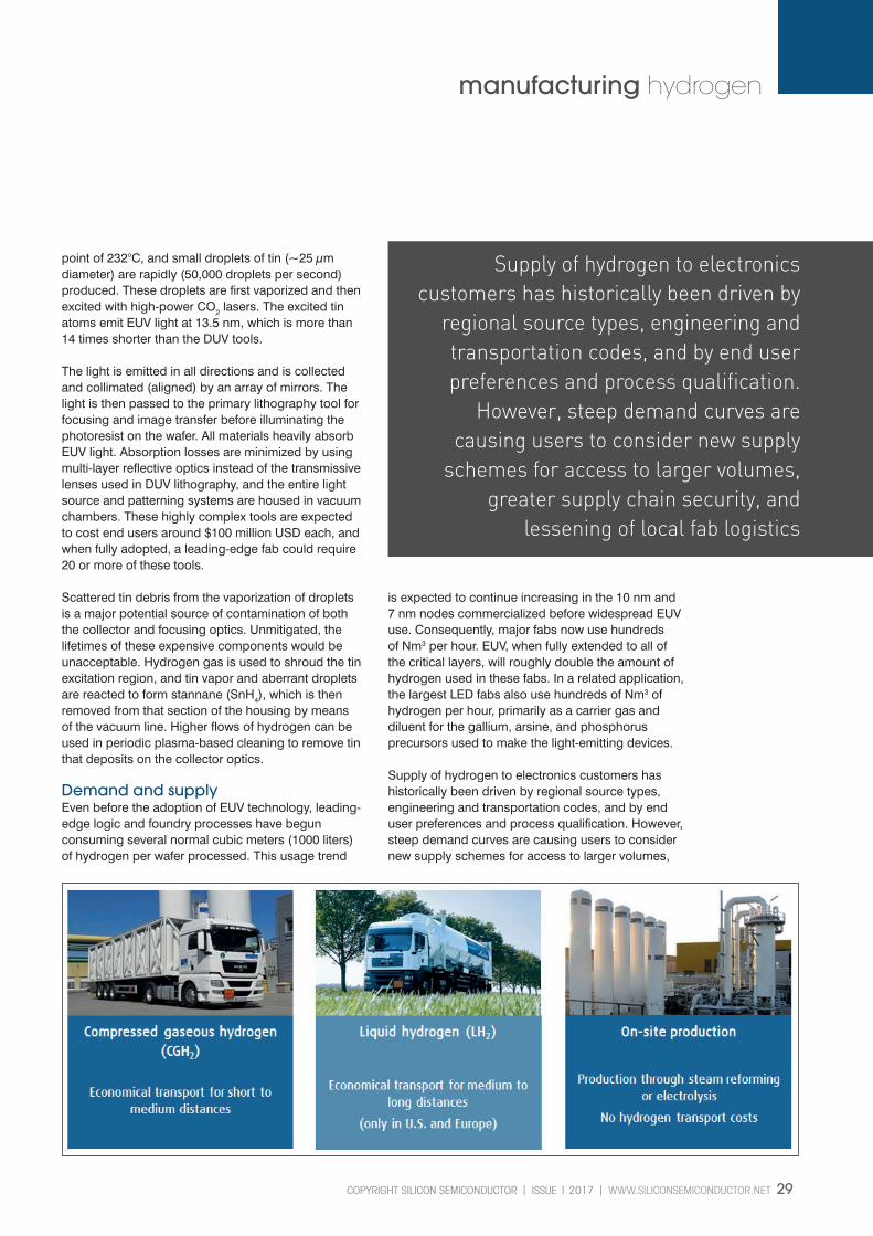
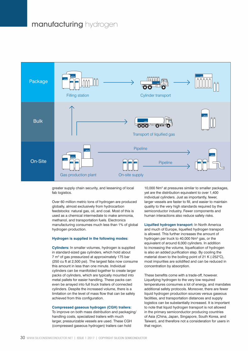
Hydrogen is supplied in the following modes:
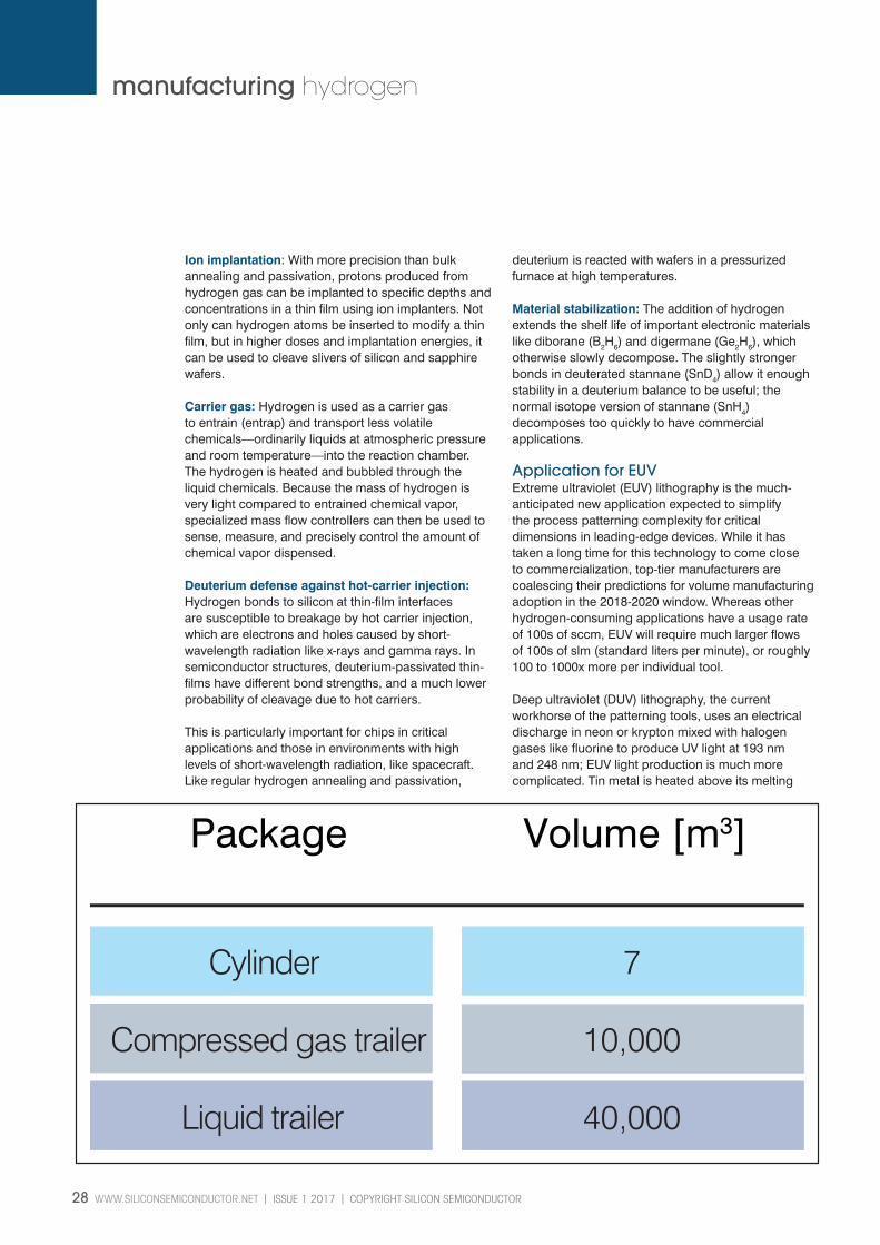
Cylinders: In smaller volumes, hydrogen is supplied in standard-sized gas cylinders, which hold about 7 m3 of gas pressurized at approximately 175 bar (250 cu ft at 2,500 psi). The largest fabs now consume this amount in less than one minute. Individual cylinders can be manifolded together to create larger packs of cylinders, which are typically mounted into metal pallets for easier handling. These packs can even be arrayed into full truck trailers of connected cylinders. Despite the increased volume, there is a limitation on the level of mass flow that can be safely achieved from this configuration.
Compressed gaseous hydrogen (CGH) trailers: To improve on both mass distribution and packaging/handling costs, specialized trailers with much larger, pressurizable vessels are used. These CGH (compressed gaseous hydrogen) trailers can hold
10,000 Nm3 at pressures similar to smaller packages, yet are the distribution equivalent to over 1,400 individual cylinders. Just as importantly, fewer, larger vessels are faster to fill, and easier to maintain quality to the very high standards required by the semiconductor industry. Fewer components and human interactions also reduce safety risks.
Liquified hydrogen transport: In North America and much of Europe, liquefied hydrogen transport is allowed. This further increases the amount of hydrogen per truck to 40,000 Nm3 gas, or the equivalent of around 6,000 cylinders. In addition to increasing the volume, liquefication of hydrogen is also an added purification step. By cooling the material down to the boiling point of 21 K (-252°C), most impurities are solidified and can be reduced in concentration by absorption.
These benefits come with a trade-off, however. Liquefying hydrogen to the very low required temperatures consumes a lot of energy, and mandates additional safety protocols. Moreover, there are fewer liquid hydrogen production sources versus gaseous facilities, and transportation distances and supply logistics can be substantially increased. It is important to note that liquid hydrogen transport is not allowed in the primary semiconductor producing countries of Asia (China, Japan, Singapore, South Korea, and Taiwan), and therefore not a consideration for users in that region.
COPYRIGHT SILICON SEMICONDUCTOR l ISSUE 1 2017 l WWW.SILICONSEMICONDUCTOR.NET 31
manufacturing hydrogen
On-site hydrogen production: A solution that is becoming appropriate for some fabs is on-site hydrogen production. All major fabs already have either direct on-site production of gaseous nitrogen, or are supplied via pipeline by local plants. On-site hydrogen production has similar considerations of footprint, redundancy, and back-up.
On-site hydrogen technologies suitable for semiconductor processes are either electrolysis of water or so-called “shifting” or “cracking” of hydrocarbon feedstocks. Electrolysis is relatively expensive at volume because of the energy needed to break water molecule bonds even though achieving purity in the feedstock water is relatively simple. More economical are hydrocarbon feedstocks like natural gas, LPG (liquefied petroleum gas – mostly propane and butane), and methanol. Choices for the exact plant technology depend upon the local feedstocks available and the customer quality profile requirements.
Regardless of whether the hydrogen is supplied in gaseous or liquefied containers or made on-site, semiconductor hydrogen supply schemes incorporate on-site, and often additional point-of-use, purification using various technologies: adsorption, gettering, and application of the unique property of hydrogen to diffuse through palladium metal membranes, which are impervious to most other molecules.
In addition, hydrogen purity is monitored at several points in the distribution by multiple types of detectors. Deuterium, an isotope of hydrogen, increasingly is being used as chips are put into critical applications, and device dimensions are reduced to the atomic scale where one misplaced atom can result in chip failure. Because it is used in smaller amounts and is a very high cost material, deuterium is only packaged in individual cylinders.
Deuterium is produced by electrolysis of heavy water (D2O), which is then further dried and purified before
being compressed and packaged. Heavy water is produced primarily as a reaction moderator of certain uranium-based nuclear reactors. For higher flow applications, it can be feasible to recover deuterium from the waste stream and reprocess it off-site.
SafetyAs with all chemical supplies, safety is paramount. With hydrogen, the main safety risk is associated with its wide range of flammability and explosivity. Throughout production and packaging, multiple types of redundant protocols are used to ensure that no oxidizers are contacted or incorporated into the hydrogen and plant designs minimize the risk for leaks.
Specialized clothing resistant to fire and static is worn in some hydrogen producing and using environments. Materials of construction and component qualification are also important to guard against a phenomenon known as hydrogen embrittlement, where at elevated temperatures and/or pressures, hydrogen can permeate and weaken certain metals and alloys. Finally, liquefied hydrogen introduces the additional risk associated with cryogenic materials and the need to use insulating vessels and personal protection.
ConclusionSemiconductor manufacturing has long used hydrogen in an essential and expanding portfolio of applications. The supply of hydrogen is already a bulk material scheme, with source, transport, and logistic considerations.
The adoption of EUV at leading-edge fabs in the next few years will accelerate the pace of hydrogen consumption, and drive the consideration of new supply schemes. End users should evaluate hydrogen supply options for future fabs as part of their advanced planning to ensure that their quality, supply, and process integrity requirements will be met.
© 2017 Angel Business Communications.Permission required.
The Linde Group provides its customers with the most comprehensive package of hydrogen supply and technology. Linde manages a large and diverse portfolio
of hydrogen producing and transport assets, supplying the semiconductor industry in Asia, Europe, and North America. Linde Kryotechnik pioneered hydrogen liquefaction, and has supplied over 1,000 cryogenic hydrogen plants globally. Linde Engineering is a leading technology partner for plant
engineering and construction, including the production of hydrogen from multiple feedstocks designed into modular and automated on-site plants. Linde Gas is the world’s leading civilian producer and supplier of deuterium. Linde Electronics supplies hydrogen to its electronics customers as part of a material offering of over 100 gas and chemicals with the highest safety, quality, and reliability. Through collective management, Linde offers customers in worldwide locations access to hydrogen products when, where, and how they need them.


![2012 Determination - Home - Linde España | Linde España · Linde financiaL highLights [1] Linde financiaL highL ights Linde financial highlights January to december 2012 2011 change](https://static.fdocuments.net/doc/165x107/5f9a3ff2e98e362cc85a459b/2012-determination-home-linde-espaa-linde-espaa-linde-financial-highlights.jpg)


![Use case specification dan activity diagram [INTERNAL EDUCATIONAL PURPOSED]](https://static.fdocuments.net/doc/165x107/5a6837897f8b9ae7268b4ab7/use-case-specification-dan-activity-diagram-internal-educational-purposed.jpg)