Linac Marx Modulator Update Trevor Butler 10/29/2014.
11
Linac Marx Modulator Update Trevor Butler 10/29/2014
-
Upload
emil-gordon-chambers -
Category
Documents
-
view
221 -
download
1
Transcript of Linac Marx Modulator Update Trevor Butler 10/29/2014.

Linac Marx Modulator Update
Trevor Butler10/29/2014

Overall Status• 25 Cell Modulator
– Many parts to make 25 cell modulator have arrived except;• Heat sinks (in machine shop)• New modifications (to be describe later)• Control System (presently being designed)• Enclosure (Expected to be delivered soon)
• 53 Cell – All parts except the Main Storage Capacitors and IGBT’s– 35 main storage capacitors (expected 2/1/15)– 40 IGBT switches (expected 1/1/15)
• The project WBS has to major upcoming milestones– 25 cell modulator completed 7/9/15– 53 cell modulator completed 9/4/15
• Desire to commit funds on complete design by FY15Q4• The have been significant delays to developing the modulator
– Short Circuit Current (more details to follow)– Shutdown Activities (minor slowdown)– Underestimate of required resources (control cards drafting and layout)– Personal Availability
• Presently have small percentage of Howie’s time (lead engineer)• Have majority of both Nick Gurley (electrical tech) and Kevin Roon (mechanical tech)• Need
– More engineering time from Howie– Drafting time from EE Support ORCAD drafters– Additional electrical tech to aid in assembly

Marx Modulator Cabinet for Cells
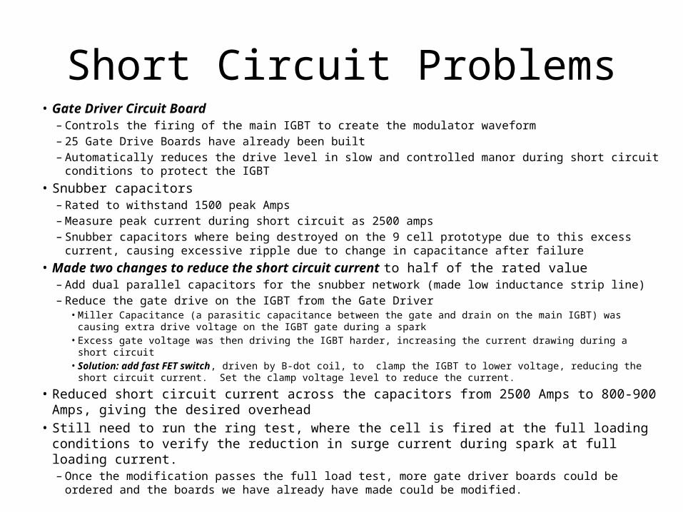
Short Circuit Problems• Gate Driver Circuit Board
– Controls the firing of the main IGBT to create the modulator waveform– 25 Gate Drive Boards have already been built– Automatically reduces the drive level in slow and controlled manor during short circuit conditions to protect
the IGBT• Snubber capacitors
– Rated to withstand 1500 peak Amps– Measure peak current during short circuit as 2500 amps– Snubber capacitors where being destroyed on the 9 cell prototype due to this excess current, causing
excessive ripple due to change in capacitance after failure• Made two changes to reduce the short circuit current to half of the rated value
– Add dual parallel capacitors for the snubber network (made low inductance strip line)– Reduce the gate drive on the IGBT from the Gate Driver
• Miller Capacitance (a parasitic capacitance between the gate and drain on the main IGBT) was causing extra drive voltage on the IGBT gate during a spark
• Excess gate voltage was then driving the IGBT harder, increasing the current drawing during a short circuit• Solution: add fast FET switch, driven by B-dot coil, to clamp the IGBT to lower voltage, reducing the short circuit current.
Set the clamp voltage level to reduce the current.
• Reduced short circuit current across the capacitors from 2500 Amps to 800-900 Amps, giving the desired overhead
• Still need to run the ring test, where the cell is fired at the full loading conditions to verify the reduction in surge current during spark at full loading current.– Once the modification passes the full load test, more gate driver boards could be ordered and the boards we
have already have made could be modified.

Single Cell Short Circuit Test

Single Cell Short Circuit Test
Without Clamping (2500 Amps) With Clamping Circuit (1700 Amps)
Ch.2 VcapCh.3 Load IGBT output voltageCh.4 Load Current (100A/V)

• Finish Individual Cell Development– Finish full current short circuit test (1 weeks engineering & 1 week elec. tech.)– Design circuit board incorporating changes (2 week elec. tech.)– Order Components (2 – 6 week delivery)– Build circuit boards (2 weeks of elec. tech. + 2 weeks of board assembly)
• Design Charging Supply System (1.2 kV, 100 kW, $165k)– Design system to meet 15 Hz, full power conditions (2 month of engineering)– Draw Schematics (3 weeks schematics)– Order components (3 days of elec. tech., followed by 2-6 weeks delivery, assuming
no long lead time items)– Build charging supply (3 weeks elec. tech.)– Test charging supply (1 week elec. tech.)– This should not hold up 25 cell testing
• Could either purchase a lower power unit and test the cells at a lower repetition rate– Running at 1 Hz reduces the power required to 7kW
• Another option is to use one of the cap chargers we already have– For example, the charging supply for the Klystron Vernier could be used– Limited to pulsing every 2-10 seconds for testing
– Would also need to build a higher power dummy load to run at full rep. rate.• Could test the 25 cell in RF7 as load to save cost and test the system in actual load
Work to build 25 Cell Modulator (1)

Work to build 25 Cell Modulator (2)• Layout Marx Control Cards (7 Cards + 1 Backplane)
– Initially thought a 25 cell kludged together modulator control system could be built, but it was decided to start development on the full 53 cell version so it could be tested on both the 25 and 53 cell version, saving both time and money
– Schematics nearing completion, layout done on 2 boards so far over past few months– Charge Control Board is presently being laid out (4 weeks layout)– Layout Remaining Boards 4 board (4 weeks layout each (16 weeks total))– Design Chassis (3 weeks mech. tech.)– Fabricate Chassis (3 weeks mech. tech.)– Design and Layout Backplane (3 weeks for schematic, 4 weeks for layout)
• Mechanically Assemble 25 cell and related interconnection bus work in Cabinet– Presently waiting for heat sinks from machine shop. Delay due to equipment failure. Act as the backplane for the
construction of each cell.– Collect parts (2 days)– Modify 25 Gate cards with modification (1 week elec. tech.). Gate cards are already stuffed.– Build 25 cells (8 weeks or elec. tech.)– Assemble Cells in Cabinet enclosure. (4 weeks of mech. tech.)
• Test 25 cell modulator– Test in lab at low repetition rate if using same load as 9 cell test
• (2 weeks elec. tech. & engineering )
– Test at 15 Hz with charging supply at full current• (1 weeks elec. tech. & engineering )
– Test at LRF7 for testing into 7835 with feedforward loop. (2 weeks)• (2 weeks elec. tech. & engineering )
– Test in LRF1 to verify feedforward operation into accelerating cavity• (2 weeks elec. tech. & engineering )

Work to build 53 Cell Modulator• Receive remaining parts to build cells
– Main Storage Capacitors• 35 remain to be delivered• Expected by 2/1/15
– IGBT switches• 40 remain to be delivered• Expected by 1/1/15
• Mechanically Assemble 28 additional cells and bus work in Cabinet– Collect parts (2 days)– Build 28 Gate cards with modification (3 weeks elec. tech.)– Build 25 cells (8 weeks elec. tech.)– Assemble Cells in Cabinet enclosure. (4 weeks of mech. tech.)
• Test 53 cell modulator– Test in lab at low repetition rate if using same load as 9 cell test
• (2 weeks elec. tech. & engineering )– Test at 15 Hz with charging supply at full current
• (1 weeks elec. tech. & engineering )– Test at LRF7 for testing into 7835 with feedforward loop. (2 weeks)
• (2 weeks elec. tech. & engineering )– Test in LRF5 to verify feedforward operation into accelerating cavity
• (2 weeks elec. tech. & engineering )

Marx Modulator Summary• 25 cell Marx labor requirements
– Engineering (Howie) – 13 weeks– Schematics (Jim B.) – 6 weeks– Elec. Tech. (Nick) – 24 weeks– Mech. Tech. (Kevin) – 10 weeks
• Could also aid Nick in building cells
– Layout Drafting (Nick or EE Support Drafting) – 24 weeks– Board Assembly – 2 weeks
• 53 cell Marx labor requirements– Engineering (Howie) – 7 weeks– Elec. Tech. (Nick) – 18 weeks
• Could be supplemented with additional technical support
– Mech. Tech. (Kevin) – 4 weeks• Could also aid Nick in building cells
• Plan to increase rate of development– Work with EE Support to emphasize the priority of the Marx modulator with PIP for the division, which
is second behind operations– Determine if and when support from EE Support Drafting can aid in creating layout– Determine if additional electrical and mechanical technical support staff is available to assist in building
the 25 cell modulator. This help could come from outside EE Support Department– Update WBS to adequately represent the labor listed above