
LIN Network for Vehicle Applications Conformance Test ...
57
SURFACE VEHICLE RECOMMENDED PRACTICE LIN Network for Vehicle Applications Conformance Test SAE Technical Standards Board Rules provide that: “This report is published by SAE to advance the state of technical and engineering sciences. The use of this report is entirely voluntary, and its applicability and suitability for any particular use, including any patent infringement arising therefrom, is the sole responsibility of the user.” SAE reviews each technical report at least every five years at which time it may be reaffirmed, revised, or cancelled. SAE invites your written comments and suggestions. Copyright © 2005 SAE International All rights reserved. No part of this publication may be reproduced, stored in a retrieval system or transmitted, in any form or by any means, electronic, mechanical, photocopying, recording, or otherwise, without the prior written permission of SAE. TO PLACE A DOCUMENT ORDER: Tel: 877-606-7323 (inside USA and Canada) Tel: 724-776-4970 (outside USA) Fax: 724-776-0790 Email: [email protected] SAE WEB ADDRESS: http://www.sae.org Issued 2005-09 ® J2602-2 ISSUED SEP2005 TABLE OF CONTENTS 1. Scope ..................................................................................................................................... 3 1.1 Mission/Theme ....................................................................................................................... 4 1.2 Overview ................................................................................................................................ 4 1.3 Relationship to the LIN Conformance Test Specification ...................................................... 4 1.3.1 LIN OSI Layer 1 – Physical Layer .......................................................................................... 4 1.3.2 LIN OSI Layer 2 – Data Link Layer ........................................................................................ 5 1.3.3 Node Configuration / Network Management......................................................................... 5 1.3.4 LIN EMC Test Specification ................................................................................................... 5 1.4 Rationale ................................................................................................................................ 5 2. References ............................................................................................................................. 5 2.1 Applicable Publications .......................................................................................................... 5 2.1.1 SAE Publications.................................................................................................................... 5 2.1.2 ISO Documents ...................................................................................................................... 5 2.1.3 Supplier Publications.............................................................................................................. 5 2.1.4 Other Publications .................................................................................................................. 6 3. Definition of Terms ................................................................................................................. 6 3.1 Glossary ................................................................................................................................. 6 4. Acronyms, Abbreviations, and Symbols ................................................................................ 6 5. LIN System Requirements ..................................................................................................... 7 5.1 LIN Specification Package ..................................................................................................... 7 5.2 J2602 Serial Data Link Characteristics .................................................................................. 7 5.3 Detection of Errors by Master (ref Section 4.1, LIN 2.0 Protocol Specification) .................... 7 5.4 Frame Processing by Slave Tasks (ref Section 4.2.2, LIN 2.0 Protocol Specification) ......... 8 5.4.1 Slave Node Error Behavior .................................................................................................... 8 5.4.2 Slave Task in a Master Node Error Behavior ...................................................................... 11 5.5 Master and Slave Message Transmission Time Tolerance (ref. Section 2.2, LIN 2.0 Protocol Specification) ......................................................................................................... 12 5.6 LIN Product Identification (ref. Section 2.4, LIN 2.0 Diag and Config Specification) ........... 13 Licensed to Nanyang Tech University Licensed from the SAE Digital Library Copyright 2010 SAE International E-mailing, copying and internet posting are prohibited Downloaded Sunday, September 19, 2010 6:50:55 PM Author:Gilligan-SID:9234-GUID:35989776-155.69.4.4
Transcript of LIN Network for Vehicle Applications Conformance Test ...

SURFACE VEHICLE RECOMMENDED PRACTICE
LIN Network for Vehicle Applications Conformance Test
SAE Technical Standards Board Rules provide that: “This report is published by SAE to advance the state of technical and engineering sciences. The use of this report is entirely voluntary, and its applicability and suitability for any particular use, including any patent infringement arising therefrom, is the sole responsibility of the user.” SAE reviews each technical report at least every five years at which time it may be reaffirmed, revised, or cancelled. SAE invites your written comments and suggestions. Copyright © 2005 SAE International All rights reserved. No part of this publication may be reproduced, stored in a retrieval system or transmitted, in any form or by any means, electronic, mechanical, photocopying, recording, or otherwise, without the prior written permission of SAE. TO PLACE A DOCUMENT ORDER: Tel: 877-606-7323 (inside USA and Canada) Tel: 724-776-4970 (outside USA) Fax: 724-776-0790 Email: [email protected] SAE WEB ADDRESS: http://www.sae.org
Issued 2005-09
® J2602-2
ISSUED SEP2005
TABLE OF CONTENTS
1. Scope ..................................................................................................................................... 3 1.1 Mission/Theme....................................................................................................................... 4 1.2 Overview ................................................................................................................................ 4 1.3 Relationship to the LIN Conformance Test Specification ...................................................... 4 1.3.1 LIN OSI Layer 1 – Physical Layer.......................................................................................... 4 1.3.2 LIN OSI Layer 2 – Data Link Layer ........................................................................................ 5 1.3.3 Node Configuration / Network Management......................................................................... 5 1.3.4 LIN EMC Test Specification ................................................................................................... 5 1.4 Rationale ................................................................................................................................ 5 2. References............................................................................................................................. 5 2.1 Applicable Publications .......................................................................................................... 5 2.1.1 SAE Publications.................................................................................................................... 5 2.1.2 ISO Documents...................................................................................................................... 5 2.1.3 Supplier Publications.............................................................................................................. 5 2.1.4 Other Publications.................................................................................................................. 6 3. Definition of Terms ................................................................................................................. 6 3.1 Glossary ................................................................................................................................. 6 4. Acronyms, Abbreviations, and Symbols ................................................................................ 6 5. LIN System Requirements ..................................................................................................... 7 5.1 LIN Specification Package ..................................................................................................... 7 5.2 J2602 Serial Data Link Characteristics.................................................................................. 7 5.3 Detection of Errors by Master (ref Section 4.1, LIN 2.0 Protocol Specification).................... 7 5.4 Frame Processing by Slave Tasks (ref Section 4.2.2, LIN 2.0 Protocol Specification)......... 8 5.4.1 Slave Node Error Behavior .................................................................................................... 8 5.4.2 Slave Task in a Master Node Error Behavior ...................................................................... 11 5.5 Master and Slave Message Transmission Time Tolerance (ref. Section 2.2, LIN 2.0
Protocol Specification) ......................................................................................................... 12 5.6 LIN Product Identification (ref. Section 2.4, LIN 2.0 Diag and Config Specification)........... 13
Licensed to Nanyang Tech UniversityLicensed from the SAE Digital Library Copyright 2010 SAE International E-mailing, copying and internet posting are prohibitedDownloaded Sunday, September 19, 2010 6:50:55 PM
Author:Gilligan-SID:9234-GUID:35989776-155.69.4.4

SAE J2602-2 Issued SEP2005
- 2 -
5.7 Mandatory Node Configuration Requests (ref. LIN 2.0 Diag and Config Specification)...... 14 5.7.1 General Configuration Requirements .................................................................................. 14 5.7.2 NAD and Message ID Assignment ...................................................................................... 15 5.7.3 Targeted Reset .................................................................................................................... 21 5.7.4 Broadcast Reset Slave Response ....................................................................................... 21 5.8 Master and Slave Message Format ..................................................................................... 23 5.8.1 Checksum (ref. Section 2.1.5, LIN 2.0 Protocol Specification)............................................ 23 5.8.2 Signal Consistency (ref. Section 1.2, LIN 2.0 Protocol Specification) ................................. 23 5.8.3 Signal Encoding Types (ref. Section 1.1, LIN 2.0 Protocol Specification) ........................... 23 5.8.4 Signal Management ............................................................................................................. 23 5.8.5 Unused Bits in the Data Field (ref. Section 2.3, LIN 2.0 Protocol Specification) ................. 23 5.8.6 J2602 Slave Status Byte ...................................................................................................... 23 5.9 Message Types.................................................................................................................... 23 5.9.1 Availability of Unconditional Frames (ref Section 2.3.1, LIN 2.0 Protocol Specification) .... 23 5.9.2 Event Triggered Frames (ref. Section 2.3.2, LIN 2.0 Protocol Specification)...................... 23 5.9.3 Identifier Assignment (J2602-1 Requirement resulting from Event Triggered Frame
Anomaly) .............................................................................................................................. 23 6. J2602 API Requirements ..................................................................................................... 24 6.1 Master Node Configuration API ........................................................................................... 24 6.2 Diagnostic Transport Layer API ........................................................................................... 24 7. J2602 Bus Operation ........................................................................................................... 24 7.1 Normal Communication Mode and Transmission Rate ....................................................... 24 7.1.1 Master Node Bit Time Measurement ................................................................................... 24 7.1.2 Slave Node Bit Time Measurement ..................................................................................... 26 7.2 Sleep/Wake Mode in Master and Slave............................................................................... 28 7.2.1 Wake-up of Master and Slave (ref. Section 5.1, LIN 2.0 Protocol Specification) ................ 29 7.2.2 Go To Sleep (ref. Section 5.2, LIN 2.0 Protocol Specification)............................................ 30 7.3 LIN Controller Clock Tolerance............................................................................................ 30 7.4 Bus Electrical Parameters.................................................................................................... 31 7.4.1 LIN Bus Signals and Loading Requirements ....................................................................... 31 7.5 Master / Slave LIN Data Link (UART) Requirements .......................................................... 40 7.5.1 Sample Point ........................................................................................................................ 40 7.5.2 Synchronization.................................................................................................................... 44 7.5.3 Transmit Message Buffering ................................................................................................ 44 7.6 LIN ECU Requirements........................................................................................................ 44 7.6.1 ECU Circuit Requirements................................................................................................... 44 7.6.2 Board Layout Requirements ................................................................................................ 45 7.7 Network Topology ................................................................................................................ 45 7.7.1 Loss of ECU Ground at Master or Slave Node.................................................................... 45 7.7.2 Loss of ECU Battery............................................................................................................. 46 7.7.3 Bus Electrical Load Distribution ........................................................................................... 46 7.7.4 Bus Wiring Topology Configurations.................................................................................... 47 7.7.5 Bus Wiring Constraints......................................................................................................... 47 7.7.6 Bus Wiring Practices to Improve EMC Performance........................................................... 47 7.7.7 Bus Wiring Harness and ECU Connectors .......................................................................... 47 7.8 Master / Slave ESD Immunity .............................................................................................. 47 7.9 Master / Slave EMC Testing Requirements......................................................................... 47
Licensed to Nanyang Tech UniversityLicensed from the SAE Digital Library Copyright 2010 SAE International E-mailing, copying and internet posting are prohibitedDownloaded Sunday, September 19, 2010 6:50:55 PM
Author:Gilligan-SID:9234-GUID:35989776-155.69.4.4

SAE J2602-2 Issued SEP2005
- 3 -
7.10 Fault Tolerant Modes ........................................................................................................... 47 7.10.1 ECU Power Loss – Master / Slave....................................................................................... 48 7.10.2 Bus Wiring Short to Ground – Master / Slave...................................................................... 49 7.10.3 Bus Wiring Short to Battery.................................................................................................. 50 7.10.4 Short / Open in Other Circuits.............................................................................................. 52 7.11 Ground Offset Voltage ......................................................................................................... 52 7.12 Operating Battery Power Voltage Range............................................................................. 52 7.12.1 Normal Battery Voltage Power Operation............................................................................ 52 7.12.2 Battery Power Over-Voltage Operation ............................................................................... 54 7.12.3 Low Battery Voltage Operation ............................................................................................ 55 7.12.4 Battery Offset Voltage .......................................................................................................... 56 7.12.5 Reverse Battery Blocking Diode .......................................................................................... 56 7.13 Environmental Requirements............................................................................................... 56 7.13.1 Transmit Operating Conditions ............................................................................................ 56
Foreword
The objective of this document is to define a standard conformance test for J2602-1 devices.
The goal of this document is to define a basic conformance test for J2602-1 Master and Slave nodes that can be used to determine the suitability of devices for use. This is not a complete Qualification test. This does not replace the individual suppliers’ IC and/or module qualification.
1. Scope
This document covers the tests to be performed on all J2602-1 defined Master and Slave nodes. Tests described in this document will ensure a minimum standard level of performance to which all compatible ECUs and media shall be designed. This will assure full serial data communication among all connected devices regardless of supplier.
The goal of SAE J2602-2 is to improve the interoperability and interchangeability of LIN devices within a network by verifying the devices pass a minimum set of tests.
To allow for easy cross-reference, this document is arranged such that the conformance test for a given section in J2602-1 is in the same section in J2602-2.
This document is to be referenced by the particular vehicle OEM component technical specification that describes any given ECU in which the LIN data link controller and physical layer interface is located. Primarily, the performance of the physical layer is specified in this document. ECU environmental and other requirements, when provided in the component technical specification, shall supercede the requirements of this document.
The intended audience includes, but is not limited to, ECU suppliers, LIN controller suppliers, LIN transceiver suppliers, component release engineers and vehicle system engineers.
Licensed to Nanyang Tech UniversityLicensed from the SAE Digital Library Copyright 2010 SAE International E-mailing, copying and internet posting are prohibitedDownloaded Sunday, September 19, 2010 6:50:55 PM
Author:Gilligan-SID:9234-GUID:35989776-155.69.4.4

SAE J2602-2 Issued SEP2005
- 4 -
1.1 Mission/Theme
This serial data link network is intended for use in applications where high data rate is not required and a lower data rate can achieve cost reductions in both the physical media components and in the microprocessor and/or dedicated logic devices (ASICs) which use the network.
1.2 Overview
LIN is a single wire, low cost, Class A communication protocol. LIN is a master-slave protocol, and utilizes the basic functionality of most Universal Asynchronous Receiver Transmitter (UART) or Serial Communication Interface (SCI) devices as the protocol controllers in both Master and Slave devices. To meet the target of “Lower cost than either an OEM proprietary communications link or CAN link” for low speed data transfer requirements, a single wire transmission media based on the ISO 9141 specification was chosen. The protocol is implemented around a UART/SCI capability set, because the silicon footprint is small (lower cost). Many small microprocessors are equipped with either a UART or SCI interface (lower cost), and the software interface to these devices is relatively simple to implement (lower software cost). Finally, the relatively simplistic nature of the protocol controller (UART/SCI) and the nature of state-based operation, enable the creation of Application Specific Integrated Circuits (ASICs) to perform as input sensor gathering and actuator output controlling devices, in the vein of Mechatronics.
All message traffic on the bus is initiated by the Master device. Slave devices receive commands and respond to requests from the Master. Since the Master initiates all bus traffic, it follows that the Slaves cannot communicate unless requested by the Master. However, Slave devices can generate a bus wakeup, if their inherent functionality requires this feature.
The “LIN Consortium” developed the set of LIN specifications. The Consortium is a group of automotive OEMs, semiconductor manufacturers, and communication software and tool developers. The LIN specification set is “released” by the LIN Steering Committee, a closed subset of the members. Associate Consortium members contribute to the formation of the specifications through participation in LIN Work Groups; however, the direction of the Work Groups and the final released content of the specifications is the responsibility of the LIN Steering Committee.
The LIN Conformance Test Specification contains tests for the Physical Layer, Data Link Layer, Node Configuration and Network Management, and EMC.
1.3 Relationship to the LIN Conformance Test Specification
The LIN Conformance Test Specification Package, version 1.0 dated August 1, 2004, consists of four documents:
1.3.1 LIN OSI LAYER 1 – PHYSICAL LAYER
The LIN OSI Layer 1 – Physical Layer Test Specification describes the tests to be performed on the physical layer characteristics, including operating voltage range, signal threshold values, slope control, propagation delay, power and ground voltage shifts, fault conditions, etc.
Licensed to Nanyang Tech UniversityLicensed from the SAE Digital Library Copyright 2010 SAE International E-mailing, copying and internet posting are prohibitedDownloaded Sunday, September 19, 2010 6:50:55 PM
Author:Gilligan-SID:9234-GUID:35989776-155.69.4.4

SAE J2602-2 Issued SEP2005
- 5 -
1.3.2 LIN OSI LAYER 2 – DATA LINK LAYER
The LIN OSI Layer 2 – Data Link Layer Test Specification describes the tests to be performed on the data link layer including timing parameters, communication with no errors present, behavior in the presence of errors, etc.
1.3.3 NODE CONFIGURATION / NETWORK MANAGEMENT
The Node Configuration / Network Management Test Specification describes the tests to be performed to verify proper Node Configuration and Network Management including Error Status Management, Sleep and Wake-up behavior and Node Configuration.
1.3.4 LIN EMC TEST SPECIFICATION
The LIN EMC Test Specification describes the EMC tests to be performed on LIN 2.0 devices. None of these tests apply to J2602-1 devices.
The remainder of this document (SAE J2602-2) will directly reference these LIN specifications.
1.4 Rationale
Not applicable.
2. References
2.1 Applicable Publications
The following publications form a part of this specification to the extent specified herein. Unless otherwise indicated, the latest version of SAE publications shall apply.
2.1.1 SAE PUBLICATIONS
Available from SAE, 400 Commonwealth Drive, Warrendale, PA 15096-0001 or www.sae.org. SAE J1213-1—Glossary of Vehicle Networks for Multiplexing and Data Communication SAE J1930—Electrical/Electronic Systems Diagnostic Terms, Definitions, Abbreviations and Acronyms SAE J2602-1—LIN Network for Vehicle Applications
2.1.2 ISO DOCUMENTS
Available from ANSI, 25 West 43rd Street, New York, NY 10036-8002 or www.iso.org. ISO 9141—Road vehicles—Diagnostic systems—Requirements for interchange of digital information
2.1.3 SUPPLIER PUBLICATIONS
See Appendix A for list of supplier documents/devices.
Licensed to Nanyang Tech UniversityLicensed from the SAE Digital Library Copyright 2010 SAE International E-mailing, copying and internet posting are prohibitedDownloaded Sunday, September 19, 2010 6:50:55 PM
Author:Gilligan-SID:9234-GUID:35989776-155.69.4.4

SAE J2602-2 Issued SEP2005
- 6 -
2.1.4 OTHER PUBLICATIONS LIN Specification Package version 2.0 dated September 23, 2003 available at www.lin-subbus.org. LIN Conformance Test Specification for LIN 2.0 dated August 1, 2004 available to members of the LIN
consortium at www.lin-subbus.org. ES-XW7T-1A278-AC—Ford Component and Subsystem Electromagnetic Compatibility Worldwide
Requirements and Test Procedures available at www.fordemc.com. This document shall be referred to as the Ford EMC Spec.
3. Definition of Terms
3.1 Glossary
3.1.1 AGING FACTOR OF THE CLOCK
This is provided by the supplier of the clock device (crystal, ceramic resonator, etc.) and is the portion of the maximum total clock tolerance over the device lifetime due to aging (time).
4. Acronyms, Abbreviations, and Symbols 1. API – Application Program Interface 2. ASIC – Application Specific Integrated Circuit 3. CAN – Controller Area Network 4. CTS – Component Technical Specification 5. DLC – Diagnostic Link Connector 6. DNN – Device Node Number 7. DUT – Device Under Test 8. ECU – Electronic Control Unit 9. EMC – Electromagnetic Compatibility 10. ESD – Electrostatic Discharge 11. ISO – International Organization for Standardization 12. Kbits/sec – Thousands of data bits per second 13. LDF – LIN Description File 14. LIN – Local Interconnect Network 15. LSB – Least Significant Byte 16. lsb – least significant bit 17. MSB – Most Significant Byte 18. msb – most significant bit 19. NAD – Node Address for Diagnostics 20. NCF – Node Capability File 21. OEM – Original Equipment Manufacturer 22. RE – Radiated Emissions 23. RI – Radiated Immunity 24. SAE – Society of Automotive Engineers 25. SCI – Serial Communication Interface 26. UART – Universal Asynchronous Receiver/Transmitter
Licensed to Nanyang Tech UniversityLicensed from the SAE Digital Library Copyright 2010 SAE International E-mailing, copying and internet posting are prohibitedDownloaded Sunday, September 19, 2010 6:50:55 PM
Author:Gilligan-SID:9234-GUID:35989776-155.69.4.4

SAE J2602-2 Issued SEP2005
- 7 -
5. LIN System Requirements
General Test Assumptions 1. All slave devices shall have at least one request message to which they respond. 2. The Cload and Rload values specified shall include the characteristics of the test tool, so that this is the
entire load external to the DUT. 3. All slave devices are assumed to contain 220 pF nominal capacitances.
5.1 LIN Specification Package
This section is informative in nature and does not require any tests.
5.2 J2602 Serial Data Link Characteristics
This section is informative in nature and does not require any tests.
5.3 Detection of Errors by Master (ref Section 4.1, LIN 2.0 Protocol Specification)
This test verifies that the Master DUT stops transmitting the header when the Synch symbol is not $55 or when there is a framing error in the Synch symbol (STOP bit = 0).
Power Supply
VECU
LIN
GND
Measurement
Bus LoadMaster
ECUCload
Rload
LIN tool
FIGURE 1—DETECTION OF ERRORS BY MASTER TEST SETUP
Licensed to Nanyang Tech UniversityLicensed from the SAE Digital Library Copyright 2010 SAE International E-mailing, copying and internet posting are prohibitedDownloaded Sunday, September 19, 2010 6:50:55 PM
Author:Gilligan-SID:9234-GUID:35989776-155.69.4.4

SAE J2602-2 Issued SEP2005
- 8 -
TABLE 1—DETECTION OF ERRORS BY MASTER TEST PLAN
DUT node as
Master ECU With C = 220pF
Test case 5.3.x (2 cases)
Parameter VECU Rload and Cload
12V 20 kΩ, 220 pF
Test Steps See Table 1 Response See Table 1 Reference J2602-1 Section 5.3
# Test Test Steps Response
5.3.1 1. DUT sends out any message. 2. Test tool sends out a $F0 data byte when a
Start bit is detected after the break symbol
The DUT should not transmit the ID. The next thing transmitted by the DUT should be a Break/Sync symbol.
5.3.2 1. DUT sends out any message. 2. Test tool corrupts the stop bit of the Sync
Byte.
The DUT should not transmit the ID. The next thing transmitted by the DUT should be a Break/Sync symbol.
5.4 Frame Processing by Slave Tasks (ref Section 4.2.2, LIN 2.0 Protocol Specification)
5.4.1 SLAVE NODE ERROR BEHAVIOR
The purposes of this test are to: 1. Verify that the slave DUT stops transmission when an error ocurs during transmission and sets the
appropriate error code in the J2602 Status Byte. 2. Verify that the slave DUT recognizes an error in a received message and sets the appropriate error
code in the J2602 Status Byte. 3. Verify that the slave DUT does not transmit when the Synch byte is anything other than $55 and sets
the appropriate error code in the J2602 Status Byte.
Licensed to Nanyang Tech UniversityLicensed from the SAE Digital Library Copyright 2010 SAE International E-mailing, copying and internet posting are prohibitedDownloaded Sunday, September 19, 2010 6:50:55 PM
Author:Gilligan-SID:9234-GUID:35989776-155.69.4.4

SAE J2602-2 Issued SEP2005
- 9 -
Power Supply
VECU
LIN
GND
Measurement
Bus LoadSlave
ECUCload
Rload
LIN tool
FIGURE 2—SLAVE NODE ERROR BEHAVIOR TEST SETUP
TABLE 2—SLAVE NODE ERROR BEHAVIOR TEST PLAN
DUT node as
Slave ECU With C = 220pF
Test case 5.4.1.x (5 cases)
Parameter VECU Rload and Cload
12V 1 kΩ, 220 pF
Test Steps See Table 2 Response See Table 2 Reference J2602-1 Section 5.4
# Test Test Steps Response
5.4.1.1 1. Verify no error codes are set in the slave by sending a slave specific request message ID for DUT and checking the Status Byte. There are no error codes set when the most significant bit of the Status Byte is ‘0’. Repeat until no errors are found.
2. Send a $3C Targeted Reset to the DUT 3. Send a $3D Response with the ID Parity bits
corrupted, i.e. Protected ID of (0011 1101) 4. Send a slave specific request message ID for
DUT without error.
After step 3 the DUT should not send any data. After step 4 the Status Byte returned by the DUT should be (111x xxxx).
Licensed to Nanyang Tech UniversityLicensed from the SAE Digital Library Copyright 2010 SAE International E-mailing, copying and internet posting are prohibitedDownloaded Sunday, September 19, 2010 6:50:55 PM
Author:Gilligan-SID:9234-GUID:35989776-155.69.4.4

SAE J2602-2 Issued SEP2005
- 10 -
TABLE 2—SLAVE NODE ERROR BEHAVIOR TEST PLAN (CONTINUED)
# Test Test Steps Response 5.4.1.2 1. Verify no error codes are set in the slave by
sending a slave specific request message ID for DUT and checking the Status Byte. There are no error codes set when the most significant bit of the Status Byte is ‘0’. Repeat until no errors are found.
2. Send a $3C Targeted Reset to the DUT 3. Send a $3D Response and corrupt the Stop bit
(transmit a dominant) of the NAD byte sent by the DUT.
4. Send a slave specific request message ID for DUT without error.
After step 3 the DUT should not transmit another byte after the NAD. After step 4 the Status Byte returned by the DUT should be (110x xxxx).
5.4.1.3 1. Verify no error codes are set in the slave by sending a slave specific request message ID for DUT and checking the Status Byte. There are no error codes set when the most significant bit of the Status Byte is ‘0’. Repeat until no errors are found.
2. Send a $3C Targeted Reset with a corrupted checksum to the DUT
3. Send a slave specific request message ID for DUT without error.
After step 3 the Status Byte returned by the DUT should be (101x xxxx).
5.4.1.4 1. x = 0 2. Verify no error codes are set in the slave by
sending a slave specific request message ID for DUT and checking the Status Byte. There are no error codes set when the most significant bit of the Status Byte is ‘0’. Repeat until no errors are found.
3. Send a $3C Targeted Reset to the DUT 4. Send a $3D Response with sync byte = x. 5. Send a slave specific request message ID for
DUT without error. 6. x = x + 1 7. If x <= 257 goto 2, else END.
After step 4 the DUT should only transmit if the sync byte transmitted was $55. After step 5 the Status Byte returned by the DUT should be (100x xxxx) if the device has a fixed clock. Alternatively, if the device is performing autobauding the Status Byte returned may be (000x xxxx).
5.4.1.5 1. Verify no error codes are set in the slave by sending a slave specific request message ID for DUT and checking the Status Byte. There are no error codes set when the most significant bit of the Status Byte is ‘0’. Repeat until no errors are found.
2. Send a $3C Targeted Reset to the DUT 3. Send a $3D Response and corrupt bit 6 (send
a dominant) of the NAD byte sent by the DUT. 4. Send a slave specific request message ID for
DUT without error.
After step 3 the DUT should not transmit another byte after the NAD. After step 4 the Status Byte returned by the DUT should be (100x xxxx).
Licensed to Nanyang Tech UniversityLicensed from the SAE Digital Library Copyright 2010 SAE International E-mailing, copying and internet posting are prohibitedDownloaded Sunday, September 19, 2010 6:50:55 PM
Author:Gilligan-SID:9234-GUID:35989776-155.69.4.4

SAE J2602-2 Issued SEP2005
- 11 -
5.4.2 SLAVE TASK IN A MASTER NODE ERROR BEHAVIOR
This test verifies that the Master DUT stops transmitting when there is an error in the Protected Identifier, a framng error in any data byte, or a data bit is corrupted.
Power Supply
VECU
LIN
GND
Measurement
Bus LoadMaster
ECUCload
Rload
LIN tool
FIGURE 3—SLAVE TASK IN A MASTER NODE ERROR BEHAVIOR TEST SETUP
TABLE 3—SLAVE TASK IN A MASTER NODE ERROR BEHAVIOR TEST PLAN
DUT node as
Master ECU With C = 220pF
Test case 5.4.2.x (3 cases)
Parameter VECU Rload and Cload
12V 20 kΩ, 220 pF
Test Steps See Table 3 Response See Table 3 Reference J2602-1 Section 5.4
Licensed to Nanyang Tech UniversityLicensed from the SAE Digital Library Copyright 2010 SAE International E-mailing, copying and internet posting are prohibitedDownloaded Sunday, September 19, 2010 6:50:55 PM
Author:Gilligan-SID:9234-GUID:35989776-155.69.4.4

SAE J2602-2 Issued SEP2005
- 12 -
TABLE 3—SLAVE TASK IN A MASTER NODE ERROR BEHAVIOR TEST PLAN (CONTINUED)
# Test Test Steps Response 5.4.2.1 Corrupt the parity of the ID byte of any Command
Message initiated by the DUT. The DUT should not transmit any other bytes of this message. The next thing transmitted by the DUT should be a Break/Sync symbol.
5.4.2.2 Corrupt the stop bit of any data byte of any Command Message initiated by the DUT.
The DUT should not transmit any other bytes of this message. The next thing transmitted by the DUT should be a Break/Sync symbol.
5.4.2.3 Corrupt any single data bit of any data byte of any Command Message initiated by the DUT.
The DUT should not transmit any other bytes of this message. The next thing transmitted by the DUT should be a Break/Sync symbol.
5.5 Master and Slave Message Transmission Time Tolerance (ref. Section 2.2, LIN 2.0 Protocol Specification)
Test according to LIN Conformance Test Specification LIN OSI Layer 2 – Data Link Layer Version 1.0 of August 1, 2004 Sections 2.1, 2.2, 2.3, 2.4, 2.5, 2.6 and 2.10.
Use the following messages for the Test Frames called out in these sections:
TABLE 4—TEST FRAME ASSIGNMENTS
TST_Frame Requirements for the Test Frame TST_FRAME_1 Any frame sent by the master TST_FRAME_2 Targeted Reset TST_FRAME_3 Not Used TST_FRAME_4 Device Specific Frame, reference NCF TST_FRAME_5 Not Used TST_FRAME_6 Slave Response Command Frame, Identifier = 0x3D TST_FRAME_7 Not Used TST_FRAME_8 Not Used TST_FRAME_9 Command Frame Sleep Request, Identifier = 0x3C, NAD = 0x00
Licensed to Nanyang Tech UniversityLicensed from the SAE Digital Library Copyright 2010 SAE International E-mailing, copying and internet posting are prohibitedDownloaded Sunday, September 19, 2010 6:50:55 PM
Author:Gilligan-SID:9234-GUID:35989776-155.69.4.4

SAE J2602-2 Issued SEP2005
- 13 -
Use the following values for the variables in these sections:
TABLE 5—TEST VARIABLE TIMES
Parameter Time TSYNBRK_MIN 1241.76 µs TSYNBRK_MAX 2566.37 µs TSYNDEL_MIN 95.52 µs TSYNDEL_MAX 1408.61 µs THEADER_NOMINAL 3264 µs THEADER_MAXIMUM 4592.45 µs TFRAME_NOMINAL 11904 µs TFRAME_MAXIMUM THEADER_MAXIMUM +
safety_factor * 72 * max clock tol.
40 bits 3840 µs 20 bits 1920 µs 19 bits 1824 µs 15 bits 1440 µs 13 bits 1248 µs 10 bits 960 µs 8 bits 768 µs 6 bits 576 µs 3 bits 288 µs 2 bits 192 µs
Section 2.1 – Use as is.
Section 2.2 – Use as is.
Section 2.3 – Use as is.
Section 2.4 – Use as is.
Section 2.5 – Use as is.
Section 2.6 – Use as is.
Section 2.10 – Use as is.
5.6 LIN Product Identification (ref. Section 2.4, LIN 2.0 Diag and Config Specification)
Decided by review by end user.
Licensed to Nanyang Tech UniversityLicensed from the SAE Digital Library Copyright 2010 SAE International E-mailing, copying and internet posting are prohibitedDownloaded Sunday, September 19, 2010 6:50:55 PM
Author:Gilligan-SID:9234-GUID:35989776-155.69.4.4

SAE J2602-2 Issued SEP2005
- 14 -
5.7 Mandatory Node Configuration Requests (ref. LIN 2.0 Diag and Config Specification)
5.7.1 GENERAL CONFIGURATION REQUIREMENTS
5.7.1.1 Slave Execution of Configuration
This test verifies that the slave DUT will perform the $3C command without receiving a $3D request using the Targeted Reset Command.
Power Supply
VECU
LIN
GND
Measurement
Bus LoadSlave
ECUCload
Rload
LIN tool
FIGURE 4—SLAVE EXECUTION OF CONFIGURATION TEST SETUP
TABLE 6—SLAVE EXECUTION OF CONFIGURATION TEST PLAN
DUT node as
Slave ECU With C = 220pF
Test case 5.7.1.1
Parameter VECU Rload and Cload
12V 1 kΩ, 220 pF
Test Steps See Table 6 Response See Table 6 Reference J2602-1 Section 5.7.1.1
Licensed to Nanyang Tech UniversityLicensed from the SAE Digital Library Copyright 2010 SAE International E-mailing, copying and internet posting are prohibitedDownloaded Sunday, September 19, 2010 6:50:55 PM
Author:Gilligan-SID:9234-GUID:35989776-155.69.4.4

SAE J2602-2 Issued SEP2005
- 15 -
TABLE 6—SLAVE EXECUTION OF CONFIGURATION TEST PLAN (CONTINUED)
# Test Test Steps Response 5.7.1.1 1. Verify no error codes are set in the slave by
sending a slave specific request message ID for DUT and checking the Status Byte. There are no error codes set when the most significant bit of the Status Byte is ‘0’. Repeat until no errors are found.
2. Send a $3C Targeted Reset to the DUT. Do not follow this with a $3D request.
3. Send a slave specific request message ID for DUT without error.
After step 3 the Status Byte returned by the DUT should be (001x xxxx). This verifies that the reset was performed without the device receiving a $3D.
5.7.1.2 Slave Device Configuration Capabilities
Verify NCF is available and complete.
5.7.1.3 Master Configuration Message Pairing
Application software specific.
5.7.2 NAD AND MESSAGE ID ASSIGNMENT
5.7.2.1 Slave NAD Assignment
Devices which have a Hardware Selectable DNN and are also configurable via software should be conformance tested via Sections 5.7.2.1.1 and 5.7.2.1.3. This may require that two devices be tested, one for each test section performed. Please see the NCF to determine if the Hardware Selection or Software Configuration has a higher priority. The supplier of the device shall provide a method of testing the device to ensure that the NCF description of priority is correctly implemented.
Licensed to Nanyang Tech UniversityLicensed from the SAE Digital Library Copyright 2010 SAE International E-mailing, copying and internet posting are prohibitedDownloaded Sunday, September 19, 2010 6:50:55 PM
Author:Gilligan-SID:9234-GUID:35989776-155.69.4.4

SAE J2602-2 Issued SEP2005
- 16 -
5.7.2.1.1 Hardware Selectable DNN
This test verifies that the DUT takes on the proper NAD based on the setting of the DNN pins.
Power Supply
VECU
LIN
GND
Measurement
Bus LoadSlave
ECUCload
Rload
LIN tool
DNN0
DNN1
DNN2
DNN3
FIGURE 5—HARDWARE SELECTABLE DNN TEST SETUP
TABLE 7—HARDWARE SELECTABLE DNN TEST PLAN
DUT node as
Slave ECU With C = 220pF
Test case 5.7.2.1.1.1
Parameter VECU Rload and Cload
12V 1 kΩ, 220 pF
Test Steps See Table 7 Response See Table 7 Reference J2602-1 Section 5.7.2.1
# Test Test Steps Response
5.7.2.1.1.1 1. set DNN = $0 2. X = $01 3. Send a $3C Targeted Reset to NAD = X 4. Send a $3D Request. 5. X = X+1 6. If X = $7F, X = X+1 7. If X <= $FF, go to 3 8. set DNN = DNN + 1 9. If DNN <=$D, go to 2
In step 4, the DUT should transmit a response when X = $6(DNN); otherwise, there should be no response sent.
Licensed to Nanyang Tech UniversityLicensed from the SAE Digital Library Copyright 2010 SAE International E-mailing, copying and internet posting are prohibitedDownloaded Sunday, September 19, 2010 6:50:55 PM
Author:Gilligan-SID:9234-GUID:35989776-155.69.4.4

SAE J2602-2 Issued SEP2005
- 17 -
5.7.2.1.2 Fixed DNN
This test verifies the NAD of the DUT.
Power Supply
VECU
LIN
GND
Measurement
Bus LoadSlave
ECUCload
Rload
LIN tool
FIGURE 6—FIXED DNN TEST SETUP
TABLE 8—FIXED DNN TEST PLAN
DUT node as
Slave ECU With C = 220pF
Test case 5.7.2.1.2.1
Parameter VECU Rload and Cload
12V 1 kΩ, 220 pF
Test Steps Perform test with each available fixed NAD See Table 8
Response See Table 8 Reference J2602-1 Section 5.7.2.1
# Test Test Steps Response
5.7.2.1.2.1 1. X = $01 2. Send a $3C Targeted Reset to NAD = X 3. Send a $3D Request. 4. X = X+1 5. If X = $7F, X = X+1 6. If X <= $FF, go to 2
In step 3, the DUT should transmit a response when X = NAD of the DUT; otherwise, there should be no response sent.
Licensed to Nanyang Tech UniversityLicensed from the SAE Digital Library Copyright 2010 SAE International E-mailing, copying and internet posting are prohibitedDownloaded Sunday, September 19, 2010 6:50:55 PM
Author:Gilligan-SID:9234-GUID:35989776-155.69.4.4

SAE J2602-2 Issued SEP2005
- 18 -
5.7.2.1.3 Software Programmable DNN
This test verifies that the DUT takes on the proper NAD based on the programmed DNN.
Power Supply
VECU
LIN
GND
Measurement
Bus LoadSlave
ECUCload
Rload
LIN tool
FIGURE 7—SOFTWARE PROGRAMMABLE DNN TEST SETUP
TABLE 9—SOFTWARE PROGRAMMABLE DNN TEST PLAN
DUT node as
Slave ECU With C = 220pF
Test case 5.7.2.1.3.1
Parameter VECU Rload and Cload
DNN
12V 1 kΩ, 220 pF $F at start of test (uninitialized device)
Test Steps See Table 9 Response See Table 9 Reference J2602-1 Section 5.7.2.1
Licensed to Nanyang Tech UniversityLicensed from the SAE Digital Library Copyright 2010 SAE International E-mailing, copying and internet posting are prohibitedDownloaded Sunday, September 19, 2010 6:50:55 PM
Author:Gilligan-SID:9234-GUID:35989776-155.69.4.4

SAE J2602-2 Issued SEP2005
- 19 -
TABLE 9—SOFTWARE PROGRAMMABLE DNN TEST PLAN (CONTINUED)
# Test Test Steps Response 5.7.2.1.3.1 1. X = $01
2. Send a $3C Targeted Reset to NAD = X 3. Send a $3D Request. 4. X = X+1 5. If X = $7F, X = X+1 6. If X <= $FF, go to 2 7. set DNN = $E (program by whatever means
the DUT uses) 8. X = $01 9. Send a $3C Targeted Reset to NAD = X 10. Send a $3D Request. 11. X = X+1 12. If X = $7F, X = X+1 13. If X <= $FF, go to 9 14. DNN = DNN – 1 (program by whatever
means the DUT uses) 15. If DNN >=$0, go to 8
In step 3, the DUT should transmit a response when X = $6F; otherwise, there should be no response sent. In step 10, the DUT should transmit a response when X = $6(DNN); otherwise, there should be no response sent.
5.7.2.2 Slave Message ID Assignment
This test verifies that the DUT takes on the proper message IDs based on its DNN.
Power Supply
VECU
LIN
GND
Measurement
Bus LoadSlave
ECUCload
Rload
LIN tool
FIGURE 8—SLAVE MESSAGE ID ASSIGNMENT TEST SETUP
Licensed to Nanyang Tech UniversityLicensed from the SAE Digital Library Copyright 2010 SAE International E-mailing, copying and internet posting are prohibitedDownloaded Sunday, September 19, 2010 6:50:55 PM
Author:Gilligan-SID:9234-GUID:35989776-155.69.4.4

SAE J2602-2 Issued SEP2005
- 20 -
TABLE 10—SLAVE MESSAGE ID ASSIGNMENT TEST PLAN
DUT node as
Slave ECU With C = 220pF
Test case 5.7.2.2.x (2 cases)
Parameter VECU Rload and Cload
12V 1 kΩ, 220 pF
Test Steps
Repeat Test for each NAD in the range $60-$6F that the device is capable of being assigned See Table 10
Response See Table 10 Reference J2602-1 Section 5.7.2.2
# Test Test Steps Response
5.7.2.2.1 1. X = $00 2. Verify no error codes are set in the slave by
sending a slave specific request message ID for DUT and checking the Status Byte. There are no error codes set when the most significant bit of the Status Byte is ‘0’. Repeat until no errors are found.
3. If message ID X is not a request message for the slave, send a message to the slave with an ID of X, 8 data bytes of $00 and a checksum of $00 (incorrect checksum), else jump to 5.
4. Send a slave specific request message to the DUT
5. X = X+1 6. If X >$3B, end 7. else, go to 3.
After step 4, if the message ID sent was a command message ID for the DUT, the Status Byte returned by the DUT should be (101x xxxx), otherwise it should be (000x xxxx).
5.7.2.2.2 1. X = $00 2. If message ID X is not a command message
to the slave, send a message header to the slave with an ID of X, else jump to 3.
3. X = X+1 4. If X >$3B, end 5. else, go to 2.
After step 2, if the message ID sent was a request message ID for the DUT, the DUT should respond with the appropriate number of bytes, otherwise the DUT should not send any response.
5.7.2.3 Slave Configuration Messages 1. When using the optional method of configuring nodes as defined in the LIN 2.0 specification, test
according to the LIN 2.0 Conformance Test Specification, Node Configuration / Network Management Sections 4.1 and 4.4.
2. When using $3C messages with NADs in the User reserved range of $80 - $FF perform the following test based on information in the node’s NCF.
3. When using $3E messages with any NAD perform the following test based on information in the node’s NCF.
Licensed to Nanyang Tech UniversityLicensed from the SAE Digital Library Copyright 2010 SAE International E-mailing, copying and internet posting are prohibitedDownloaded Sunday, September 19, 2010 6:50:55 PM
Author:Gilligan-SID:9234-GUID:35989776-155.69.4.4

SAE J2602-2 Issued SEP2005
- 21 -
Send a $3C or $3E message with the appropriate NAD based on the information in the NCF.
$3C NAD Bit 7 (msb) 6 5 4 3 2 1 Bit 0 (lsb)
1 X X X DNN3 DNN2 DNN1 DNN0
$3E NAD Bit 7 (msb) 6 5 4 3 2 1 Bit 0 (lsb)
X X X X DNN3 DNN2 DNN1 DNN0
5.7.2.4 Slave Response Message to Options 2 and 3 in Section 5.7.2.3
Verify that the $3D Response message that follows each $3C and $3E Command message returns the J2602 Status Byte (defined in Section 5.8.6 of J2602-1) in Data Byte 0. The value of the other seven data bytes is implementation dependent and beyond the scope of this specification.
Tx by Master
Tx by Slave
Tx by Slave
Tx by Slave
Tx by Slave
Tx by Slave
Tx by Slave
Tx by Slave
Tx by Slave
LIN ID Data0 Data1 Data2 Data3 Data4 Data5 Data6 Data7
$3D J2602 Status Byte
XX XX XX XX XX XX XX
5.7.2.5 Slave DNN Based Broadcast Messages
Section 5.7.2.2 checks that the slave accepts the proper LIN ID messages.
5.7.3 TARGETED RESET
This is tested in Section 7.1.2.1 or 7.1.2.2.
5.7.4 BROADCAST RESET SLAVE RESPONSE
This test verifies that the DUT accepts a Broadcast Reset Command and sets the appropriate bit in the J2602 Status Byte.
Licensed to Nanyang Tech UniversityLicensed from the SAE Digital Library Copyright 2010 SAE International E-mailing, copying and internet posting are prohibitedDownloaded Sunday, September 19, 2010 6:50:55 PM
Author:Gilligan-SID:9234-GUID:35989776-155.69.4.4

SAE J2602-2 Issued SEP2005
- 22 -
Power Supply
VECU
LIN
GND
Measurement
Bus LoadSlave
ECUCload
Rload
LIN tool
FIGURE 9—BROADCAST RESET SLAVE RESPONSE TEST SETUP
TABLE 11—BROADCAST RESET SLAVE RESPONSE TEST PLAN
DUT node as
Slave ECU With C = 220pF
Test case 5.7.4
Parameter VECU Rload and Cload
12V 1 kΩ, 220 pF
Test Steps See Table 11 Response See Table 11 Reference J2602-1 Section 5.7.4
# Test Test Steps Response
5.7.4 1. Verify no error codes are set in the slave by sending a slave specific request message ID for DUT and checking the Status Byte. There are no error codes set when the most significant bit of the Status Byte is ‘0’. Repeat until no errors are found.
2. Send a $3C Broadcast Reset to the DUT. Do not follow this with a $3D request as there would not be one.
3. Send a slave specific request message ID for DUT without error.
After step 3 the Status Byte returned by the DUT should be (001x xxxx).
Licensed to Nanyang Tech UniversityLicensed from the SAE Digital Library Copyright 2010 SAE International E-mailing, copying and internet posting are prohibitedDownloaded Sunday, September 19, 2010 6:50:55 PM
Author:Gilligan-SID:9234-GUID:35989776-155.69.4.4

SAE J2602-2 Issued SEP2005
- 23 -
5.8 Master and Slave Message Format
5.8.1 CHECKSUM (REF. SECTION 2.1.5, LIN 2.0 PROTOCOL SPECIFICATION)
If this is not correct, no other messaging would work correctly. The tool shall check the checksum in every message sent by the DUT. If the checksum is not correct an error shall be logged.
5.8.2 SIGNAL CONSISTENCY (REF. SECTION 1.2, LIN 2.0 PROTOCOL SPECIFICATION)
Not a requirement.
5.8.3 SIGNAL ENCODING TYPES (REF. SECTION 1.1, LIN 2.0 PROTOCOL SPECIFICATION)
Recommended messaging, not verifiable.
5.8.4 SIGNAL MANAGEMENT
Verified by review of the applicable NCF (Slave ECU) or LDF (Master ECU).
5.8.5 UNUSED BITS IN THE DATA FIELD (REF. SECTION 2.3, LIN 2.0 PROTOCOL SPECIFICATION)
Informational, not a requirement.
5.8.6 J2602 SLAVE STATUS BYTE
5.8.6.1 Error Field Definition
Verified proper use of Error Field Definition in Section 5.4.1.
5.8.6.2 Application Information Field
Verified by component/system level testing by the OEM/Tier 1 Supplier.
5.9 Message Types
5.9.1 AVAILABILITY OF UNCONDITIONAL FRAMES (REF SECTION 2.3.1, LIN 2.0 PROTOCOL SPECIFICATION)
This is a guideline.
5.9.2 EVENT TRIGGERED FRAMES (REF. SECTION 2.3.2, LIN 2.0 PROTOCOL SPECIFICATION)
Verified by component/system level testing by the OEM/Tier 1 Supplier.
5.9.2.1 Identifier Assignment (J2602-1 Requirement Resulting from Event Triggered Frame Anomaly)
Verified by component/system level testing by the OEM/Tier 1 Supplier.
Licensed to Nanyang Tech UniversityLicensed from the SAE Digital Library Copyright 2010 SAE International E-mailing, copying and internet posting are prohibitedDownloaded Sunday, September 19, 2010 6:50:55 PM
Author:Gilligan-SID:9234-GUID:35989776-155.69.4.4

SAE J2602-2 Issued SEP2005
- 24 -
5.9.3 SPORADIC FRAME (REF. SECTION 2.3.3, LIN 2.0 PROTOCOL SPECIFICATION)
Verified by component/system level testing by the OEM/Tier 1 Supplier.
6. J2602 API Requirements
6.1 Master Node Configuration API
Not externally verifiable, requires a software review.
6.2 Diagnostic Transport Layer API
Not a requirement.
6.3 Additional API Requirements
Not externally verifiable, requires a software review.
7. J2602 Bus Operation
The physical layer is responsible for providing a method of transferring digital data symbols (1’s and 0’s) to the communication medium. The physical layer interface is a single wire, vehicle battery referenced bus, with low side voltage drive.
7.1 Normal Communication Mode and Transmission Rate
7.1.1 MASTER NODE BIT TIME MEASUREMENT
This test verifies the bit time of the Master DUT is within the specified range under maximum and minimum bus loading conditions.
Licensed to Nanyang Tech UniversityLicensed from the SAE Digital Library Copyright 2010 SAE International E-mailing, copying and internet posting are prohibitedDownloaded Sunday, September 19, 2010 6:50:55 PM
Author:Gilligan-SID:9234-GUID:35989776-155.69.4.4

SAE J2602-2 Issued SEP2005
- 25 -
Power Supply
VECU
LIN
GND
Measurement
Bus LoadMaster
ECUCload
Rload
FIGURE 10—MASTER NODE BIT TIME MEASUREMENT TEST SETUP
TABLE 12—MASTER NODE BIT TIME MEASUREMENT TEST PLAN
DUT node as
Master ECU With C = 220pF nominal
Test case 7.1.1.x (4 cases)
Parameter VECU Rload and Cload
12V See Table 12
Test Steps
1. Sum = 0 2. Measure time from r-d edge at start bit of sync byte to final r-d edge of the sync byte
(8 bit times) t. Take measurements at 0.6 * VECU 7.2V. 3. Sum = Sum + t 4. Repeat steps 2 and 3 20 times 5. Average bit time = Sum / 20 / 8
Response See Table 12 Reference J2602-1 Section 7.1
Licensed to Nanyang Tech UniversityLicensed from the SAE Digital Library Copyright 2010 SAE International E-mailing, copying and internet posting are prohibitedDownloaded Sunday, September 19, 2010 6:50:55 PM
Author:Gilligan-SID:9234-GUID:35989776-155.69.4.4

SAE J2602-2 Issued SEP2005
- 26 -
TABLE 12—MASTER NODE BIT TIME MEASUREMENT TEST PLAN (CONTINUED)
# Test Rload Cload Response
7.1.1.1 (min tau with 15 slaves + wiring)
1.33 kΩ 1.59 nF The average bit time shall be between (96 µs (1+/- (0.005 – aging factor of clock)))
7.1.1.2 (max tau with 15 slaves + wiring)
4.00 kΩ 5.5 nF The average bit time shall be between (96 µs (1+/- (0.005 – aging factor of clock)))
7.1.1.3 (min tau with 1 slave + wiring)
20 kΩ 889 pF The average bit time shall be between (96 µs (1+/- (0.005 – aging factor of clock)))
7.1.1.4 (max tau with 1 slave + wiring)
60 kΩ 4.35 nF The average bit time shall be between (96 µs (1+/- (0.005 – aging factor of clock)))
7.1.2 SLAVE NODE BIT TIME MEASUREMENT
This test verifies the bit time of the Slave DUT is within the specified range under maximum and minimum bus loading conditions. This test also verifies that the Slave DUT can respond to a $3D request immediately following a $3C Targeted Reset command. (Requirement from Section 5.7.3 of J2602-1.)
Power Supply
VECU
LIN
GND
Measurement
Bus LoadSlave
ECUCload
Rload
LIN tool
FIGURE 11—SLAVE NODE BIT TIME MEASUREMENT TEST SETUP
Licensed to Nanyang Tech UniversityLicensed from the SAE Digital Library Copyright 2010 SAE International E-mailing, copying and internet posting are prohibitedDownloaded Sunday, September 19, 2010 6:50:55 PM
Author:Gilligan-SID:9234-GUID:35989776-155.69.4.4

SAE J2602-2 Issued SEP2005
- 27 -
7.1.2.1 Fixed Clock Slave Node
TABLE 13—SLAVE NODE BIT TIME MEASUREMENT - FIXED CLOCK TEST PLAN
DUT node as
Slave ECU With C = 220pF nominal
Test case 7.1.2.1.x (4 cases)
Parameter VECU Rload and Cload
12V See Table 13
Test Steps
1. Sum = 0 2. LIN tool transmits a Targeted Reset to the DUT 3. LIN tool transmits a $3D header to the DUT. The break character of the $3D header
shall begin within 1 bit time of the end of the stop bit of the Checksum of the $3C Targeted Reset.
4. Measure time from r-d edge at start bit of NAD to final r-d edge of the NAD (0xxxx01101) (8 bit times) t Take measurements at 0.6 * VECU 7.2V.
5. Sum = Sum + t 6. Repeat steps 2 -5 20 times 7. Average bit time = Sum / 20 / 8
Response See Table 13 Reference J2602-1 Section 7.1
# Test Rload Cload Response
7.1.2.1.1 (min tau with 15 slaves + wiring)
552 Ω 1.64 nF The average bit time shall be between (96 µs (1+/- (0.015 – aging factor of clock)))
7.1.2.1.2 (max tau with 15 slaves + wiring)
875 Ω 5.5 nF The average bit time shall be between (96 µs (1+/- (0.015 – aging factor of clock)))
7.1.2.1.3 (min tau with 1 slave + wiring)
900 Ω 889 pF The average bit time shall be between (96 µs (1+/- (0.015 – aging factor of clock)))
7.1.2.1.2 (max tau with 1 slave + wiring)
1.1 k Ω 4.35 nF The average bit time shall be between (96 µs (1+/- (0.015 – aging factor of clock)))
Licensed to Nanyang Tech UniversityLicensed from the SAE Digital Library Copyright 2010 SAE International E-mailing, copying and internet posting are prohibitedDownloaded Sunday, September 19, 2010 6:50:55 PM
Author:Gilligan-SID:9234-GUID:35989776-155.69.4.4

SAE J2602-2 Issued SEP2005
- 28 -
7.1.2.2 Autobauding Slave Node
TABLE 14—SLAVE NODE BIT TIME MEASUREMENT - AUTOBAUDING CLOCK TEST PLAN
DUT node as
Slave ECU With C = 220pF nominal
Test case 7.1.2.2.x (4 cases)
Parameter VECU Rload and Cload
12V See Table 14
Test Steps
1. SumM = 0, SumS = 0 2. LIN tool transmits a Targeted Reset to the DUT 3. LIN tool transmits a $3D header to the DUT. The break character of the $3D header
shall begin within 1 bit time of the end of the stop bit of the Checksum of the $3C Targeted Reset.
4. Measure time from r-d edge at start bit of sync byte to final r-d edge of the sync byte (8 bit times) t. Take measurements from 1 V below peak recessive voltage.
5. SumM = SumM + t 6. Measure time from r-d edge at start bit of NAD byte to final r-d edge of the NAD byte
(0xxxx01101) (8 bit times) y Take measurements from 1 V below peak recessive voltage.
7. SumS = SumS + y 8. Repeat steps 2 -5 20 times 9. Average Master bit time = SumM / 20 / 8 10. Average DUT bit time = SumS / 20 /8
Response See Table 14 Reference J2602-1 Section 7.1
# Test Rload Cload Response
7.1.2.2.1 (min tau with 15 slaves + wiring)
552 Ω 1.64 nF SumM ( 0.98) ≤ SumS ≤ SumM (1.02)
7.1.2.2.2 (max tau with 15 slaves + wiring)
875 Ω 5.5 nF SumM ( 0.98) ≤ SumS ≤ SumM (1.02)
7.1.2.2.3 (min tau with 1 slave + wiring)
900 Ω 889 pF SumM ( 0.98) ≤ SumS ≤ SumM (1.02)
7.1.2.2.4 (max tau with 1 slave + wiring)
1.1 k Ω 4.35 nF SumM ( 0.98) ≤ SumS ≤ SumM (1.02)
7.2 Sleep/Wake Mode in Master and Slave
Test according to LIN Conformance Test Specification Node Configuration / Network Management Version 1.0 of August 1, 2004 Sections 3.1, 3.2, 3.3, 3.4, 3.5 and 3.6.
Use the following messages for the Test Frames called out in these sections:
Licensed to Nanyang Tech UniversityLicensed from the SAE Digital Library Copyright 2010 SAE International E-mailing, copying and internet posting are prohibitedDownloaded Sunday, September 19, 2010 6:50:55 PM
Author:Gilligan-SID:9234-GUID:35989776-155.69.4.4

SAE J2602-2 Issued SEP2005
- 29 -
TABLE 15—TEST FRAME ASSIGNMENTS
TST_Frame Requirements for the Test Frame TST_FRAME_1 Any frame sent by the master TST_FRAME_2 Targeted Reset TST_FRAME_3 Not Used TST_FRAME_4 Device Specific Frame TST_FRAME_5 Not Used TST_FRAME_6 Slave Response Command Frame, Identifier = 0x3D TST_FRAME_7 Not Used TST_FRAME_8 Not Used TST_FRAME_9 Command Frame Sleep Request, Identifier = 0x3C, NAD = 0x00
7.2.1 WAKE-UP OF MASTER AND SLAVE (REF. SECTION 5.1, LIN 2.0 PROTOCOL SPECIFICATION)
Test according to LIN Conformance Test Specification Node Configuration / Network Management Version 1.0 of August 1, 2004 Sections 3.3, 3.4 and 3.5.
Section 3.3: Use as is.
Section 3.4: Use as is.
Section 3.5.1: Use as is.
Section 3.5.2 Verification: 1. The DUT must send the Wake Up Request according to Section 5.1, LIN 2.0 Protocol Specification. 2. If retries are supported by the DUT, the retries should meet the times specified in the following table.
After the sixth wake-up pulse the DUT should be observed for another 3 seconds to ensure that it doesn’t transmit a seventh wake-up pulse.
Parameter Minimum Maximum Wake-up Pulse 250 µs 5 ms Twu1 150 ms 300 ms Twu2 1.5 seconds 3 seconds
FIGURE 12—WAKE-UP SIGNAL TIMING
Licensed to Nanyang Tech UniversityLicensed from the SAE Digital Library Copyright 2010 SAE International E-mailing, copying and internet posting are prohibitedDownloaded Sunday, September 19, 2010 6:50:55 PM
Author:Gilligan-SID:9234-GUID:35989776-155.69.4.4

SAE J2602-2 Issued SEP2005
- 30 -
Section 3.5.3 Test: 1. The DUT is made to send a wake-up request. 2. The LIN tool sends TST_FRAME_2 after the first wake-up request. After that TST_FRAME_6 is sent
by the LIN tool.
Section 3.5.3 Verification: 1. The DUT must send the Wake Up Request according to Section 5.1, LIN 2.0 Protocol Specification. 2. The DUT must stop transmission of the wake-up request and must answer TST_FRAME_6.
7.2.2 GO TO SLEEP (REF. SECTION 5.2, LIN 2.0 PROTOCOL SPECIFICATION)
Test according to LIN Conformance Test Specification Node Configuration / Network Management Version 1.0 of August 1, 2004 Section 3.1.
Verification: 1. The DUT(Master) must send the frame without failure and the first data byte must be 0x00. 2. The DUT must not send any more messages. Observe the DUT for one complete message table
cycle time or 1 second, whichever is longer.
7.2.2.1 Slave Node Sleep
Test according to LIN Conformance Test Specification Node Configuration / Network Management Version 1.0 of August 1, 2004 Sections 3.2 and 3.6.
Section 3.2 Verification: 1. The DUT (Slave) current draw must decrease to the quiescent level as specified in the component
spec within 10 seconds unless otherwise specified in the component spec.
Section 3.6 Verification: 1. After a minimum of 4 seconds without any message traffic, the DUT (Slave) current draw must
decrease to the quiescent level as specified in the component spec within 60 seconds if the default operation is the sleep state. Otherwise, the component may continue to activate outputs, etc. as defined by the component spec.
2. In addition, the tool shall send TST_FRAME_2 followed by TST_FRAME_6 followed by the Header of TST_FRAME_2. The slave shall have the same behavior as described above.
3. Additionally, the tool shall send TST_FRAME_2 followed by TST_FRAME_6 followed by the Header of TST_FRAME_2 and the first data byte. The slave shall have the same behavior as described above.
7.3 LIN Controller Clock Tolerance
See data sheet and clock divide error.
Licensed to Nanyang Tech UniversityLicensed from the SAE Digital Library Copyright 2010 SAE International E-mailing, copying and internet posting are prohibitedDownloaded Sunday, September 19, 2010 6:50:55 PM
Author:Gilligan-SID:9234-GUID:35989776-155.69.4.4

SAE J2602-2 Issued SEP2005
- 31 -
7.4 Bus Electrical Parameters
This section describes the bus electrical voltage level parameters required by devices that drive and receive signals on the LIN bus.
7.4.1 LIN BUS SIGNALS AND LOADING REQUIREMENTS
TABLE 16—LIN BUS SIGNALS AND LOADING REQUIREMENTS
Parameter Symbol Min. Typ. Max. Units
Output High Voltage Voh 0.8 Vbatt IC Vbatt IC volts
High Voltage (Recessive) Input Threshold Vih 0.47 Vbatt IC 0.6 Vbatt IC volts
Output Low Voltage Vol 0.0 0.2 Vbatt IC volts
Low Voltage (Dominant) Input Threshold Vil 0.4 Vbatt IC 0.53 Vbatt IC volts
Input Threshold Hysteresis (Vih - Vil) 6 VHYS 0.07 Vbatt IC 0.175 Vbatt IC volts
LIN bus to Ground Isolation Resistance VL-G Iso 500 K ohms
Slave Termination Resistance RS 20 000 30 000 60 000 ohms
tREC(MAX) – tDOM(MIN)
5 Tr-d max ---- 15.9 µsec
tDOM(MAX) – tREC(MIN)
5 Td-r max ---- 17.28 µsec
7.4.1.1.1 Master Node Voh and Vol Levels Measurement
This test verifies the dominant and recessive output voltages of the Master DUT are within the specified range under maximum and minimum supply voltages.
Power Supply
VECU
LIN
GND
Measurement
Bus LoadMaster
ECUCload
Rload
FIGURE 13—MASTER NODE Voh AND Vol LEVELS MEASUREMENT TEST SETUP
Licensed to Nanyang Tech UniversityLicensed from the SAE Digital Library Copyright 2010 SAE International E-mailing, copying and internet posting are prohibitedDownloaded Sunday, September 19, 2010 6:50:55 PM
Author:Gilligan-SID:9234-GUID:35989776-155.69.4.4

SAE J2602-2 Issued SEP2005
- 32 -
TABLE 17—MASTER NODE Voh AND Vol LEVELS MEASUREMENT TEST PLAN
DUT node as
Master ECU With C = 220pF
Test case 7.4.1.1.x (2 cases)
Parameter VECU Rload Cload
See Table 17 Set to 4.0 KΩ Set to 5.5 nF
Test Steps
For each entry 1. Master Node transmits any message 2. Logic ‘1’ and Logic ‘0’ voltages are measured during the synch byte 3. Repeat steps 1-2 20 times
Response See Table 17 Reference J2602-1 Section 7.4.1
# Test VECU Response
7.4.1.1.1 8.0 V Measure Logic 1 and Logic 0 of the Synch Byte Field as shown in Figure 14. Logic 1 ≥ 5.6 Volts, Logic 0 ≤ 1.6 Volts
7.4.1.1.2 18.0 V Measure Logic 1 and Logic 0 of the Synch Byte Field as shown in Figure 14. Logic 1 ≥ 13.6 Volts, Logic 0 ≤ 3.6 Volts.
FIGURE 14—LOGIC LEVEL VOLTAGE MEASUREMENT DESCRIPTION
7.4.1.2 Slave Node Voh and Vol Levels Measurement
This test verifies the dominant and recessive output voltages of the Slave DUT are within the specified range under maximum and minimum supply voltages.
Licensed to Nanyang Tech UniversityLicensed from the SAE Digital Library Copyright 2010 SAE International E-mailing, copying and internet posting are prohibitedDownloaded Sunday, September 19, 2010 6:50:55 PM
Author:Gilligan-SID:9234-GUID:35989776-155.69.4.4

SAE J2602-2 Issued SEP2005
- 33 -
TABLE 18—SLAVE NODE Voh AND Vol LEVELS MEASUREMENT TEST PLAN
DUT node as
Slave ECU With C = 220pF
Test case 7.4.1.2.x (2 cases)
Parameter VECU Rload Cload
See Table 18 Set to 875 Ω Set to 5.5 nF
Test Steps
1. LIN tool transmits a Targeted Reset to the DUT 2. LIN tool transmits a $3D header to the DUT 3. Measure Logic ‘1’ and Logic ‘0’ voltages during the RSID byte in the DUT response. 4. Repeat steps 1-3 20 times.
Response See Table 18 Reference J2602-1 Section 7.4.1
# Test VECU Response
7.4.1.2.1 8.0 V Measure Logic 1 and Logic 0 of the RSID byte as shown in Figure 7.4.1.1. Logic 1 ≥ 5.6 Volts, Logic 0 ≤ 1.6 Volts
7.4.1.2.2 18.0 V Measure Logic 1 and Logic 0 of the RSID Byte as shown in Figure 7.4.1.1. Logic 1 ≥ 13.6 Volts, Logic 0 ≤ 3.6 Volts.
7.4.1.3 Master Node Vih Level Measurement
This test verifies the recessive input threshold of the Master DUT is within the specified range under maximum and minimum supply voltages.
Power Supply 1
VTool
LIN
GND
Oscilloscope
Bus Load
LIN TestTool
Cload
RloadMaster ECU under Test
VECU
GNDECU
LIN
Current Sinking Power Supply 2
FIGURE 15—MASTER NODE Vih LEVEL MEASUREMENT TEST SETUP
Licensed to Nanyang Tech UniversityLicensed from the SAE Digital Library Copyright 2010 SAE International E-mailing, copying and internet posting are prohibitedDownloaded Sunday, September 19, 2010 6:50:55 PM
Author:Gilligan-SID:9234-GUID:35989776-155.69.4.4

SAE J2602-2 Issued SEP2005
- 34 -
TABLE 19—MASTER NODE Vih LEVEL MEASUREMENT TEST PLAN
DUT node as
Master ECU With C = 220pF
Test case 7.4.1.3.x (2 cases)
Parameter VECU Rload Cload
See Table 19 Set to 4.0 KΩ Set to 5.5 nF
Test Steps
For each entry in Table 19: 1. Set Power Supply 2 so that the maximum LIN bus voltage is 0.8*VECU 2. Configure and allow the Master to enter sleep mode 3. Tool sends wakeup command to the master. If the master wakes up within 100 ms
(indicated by the master transmitting a message) go to step 4, if not go to step 5 4. Lower Power Supply 2 by 0.1 Volt and repeat from step 2 5. Record the last Power Supply 2 setting where the master Woke up
Response See Table 19 Reference J2602-1 Section 7.4.1
# Test VECU Response
7.4.1.3.1 8.0 V The Master must transition from waking to not waking in response to the wake up message when: 4.8 Volts ≥ Recessive LIN bus voltage ≥ 3.29 Volts
7.4.1.3.2 18.0 V The Master must transition from waking to not waking in response to the wake up message when: 10.8 Volts ≥ Recessive LIN bus voltage ≥ 7.99 Volts
NOTE—The thresholds observed in this test may not be the normal mode thresholds, but may be special sleep mode thresholds. The transceiver used in the Master should also be tested on its own or in a slave device to ensure compliance with this spec item.
7.4.1.4 Slave Node Vih Level Measurement
This test verifies the recessive input threshold of the Slave DUT is within the specified range under maximum and minimum supply voltages.
Power Supply 1
VTool
LIN
GND
Oscilloscope
Bus Load
LIN TestTool
Cload
RloadSlave ECU under Test
VECU
GNDECU
LIN
Current Sinking Power Supply 2
FIGURE 16—SLAVE NODE Vih LEVEL MEASUREMENT TEST SETUP
Licensed to Nanyang Tech UniversityLicensed from the SAE Digital Library Copyright 2010 SAE International E-mailing, copying and internet posting are prohibitedDownloaded Sunday, September 19, 2010 6:50:55 PM
Author:Gilligan-SID:9234-GUID:35989776-155.69.4.4

SAE J2602-2 Issued SEP2005
- 35 -
TABLE 20—SLAVE NODE Vih LEVEL MEASUREMENT TEST PLAN
DUT node as
Slave ECU With C = 220pF
Test case 7.4.1.4.x (2 cases)
Parameter VECU Rload Cload
See Table 20 Set to 875 Ω Set to5.5 nF
Test Steps
For each entry in Table 20: 1. Set Power Supply 2 so that the maximum LIN bus voltage is 0.8*VECU 2. LIN tool transmits a Targeted Reset to the DUT 3. LIN tool transmits a $3D header to the DUT 4. If the slave sends a response to the header go to step 5, if not go to step 6 5. Lower Power Supply 2 by 0.1 Volt and repeat from step 2 6. Record the last Power Supply 2 setting where the Slave responded to the $3D header 7. Repeat steps 1 – 6 20 times
Response See Table 20 Reference J2602-1 Section 7.4.1
# Test VECU Response
7.4.1.4.1 8.0 V The Slave must transition from responding to not responding to the $3D header when: 4.8 Volts ≥ Recessive LIN bus voltage ≥ 3.29 Volts
7.4.1.4.2 18.0 V The Slave must transition from responding to not responding to the $3D header when: 10.8 Volts ≥ Recessive LIN bus voltage ≥ 7.99 Volts
7.4.1.5 Master Node Vil Level Measurement
This test verifies the dominant input threshold of the Master DUT is within the specified range under maximum and minimum supply voltages.
Power Supply 1
VTool
LIN
GND
Oscilloscope
Bus Load
LIN TestTool
Cload
RloadMaster ECU under Test
VECU
GNDECU
LIN
Ground Offset Device
Power Supply 2
FIGURE 17—MASTER NODE Vil LEVEL MEASUREMENT TEST SETUP
Licensed to Nanyang Tech UniversityLicensed from the SAE Digital Library Copyright 2010 SAE International E-mailing, copying and internet posting are prohibitedDownloaded Sunday, September 19, 2010 6:50:55 PM
Author:Gilligan-SID:9234-GUID:35989776-155.69.4.4

SAE J2602-2 Issued SEP2005
- 36 -
TABLE 21—MASTER NODE Vil LEVEL MEASUREMENT TEST PLAN
DUT node as
Master ECU With C = 220pF
Test case 7.4.1.5.x (2 cases)
Parameter VECU Rload Cload
See Table 21 Set to 4.0 KΩ Set to 5.5 nF
Test Steps
For each entry in Table 21: 1. Set Power Supply 2 to 0.2*VECU 2. Configure and allow the Master to enter sleep mode 3. Send wakeup command to the master. If the master wakes up within 100 ms (indicated
by the master transmitting a message) go to step 4, if not go to step 5 4. Increase Power Supply 2 by 0.1 Volt and repeat step 2 5. Record the last Power Supply 2 setting where the master Woke up 6. Repeat steps 1 – 5 20 times
Response See Table 21 Reference J2602-1 Section 7.4.1
# Test VECU Response
7.4.1.5.1 8.0 V The Master must transition from waking to not waking in response to the wake up message when: 4.24 Volts ≥ Power Supply 2 ≥ 2.8 Volts
7.4.1.5.2 18.0 V The Master must transition from waking to not waking in response to the wake up message when: 9.54 Volts ≥ Power Supply 2 ≥ 6.8 Volts
NOTE—The thresholds observed in this test may not be the normal mode thresholds, but may be special sleep mode thresholds. The transceiver used in the Master should also be tested on its own or in a slave device to ensure compliance with this spec item.
7.4.1.6 Slave Node Vil Level Measurement
This test verifies the dominant input threshold of the Slave DUT is within the specified range under maximum and minimum supply voltages.
Power Supply 1
VTool
LIN
GND
Oscilloscope
Bus Load
LIN TestTool
Cload
RloadSlave ECU under Test
VECU
GNDECU
LIN
Ground Offset Device
Power Supply 2
FIGURE 18—SLAVE NODE Vil LEVEL MEASUREMENT TEST SETUP
Licensed to Nanyang Tech UniversityLicensed from the SAE Digital Library Copyright 2010 SAE International E-mailing, copying and internet posting are prohibitedDownloaded Sunday, September 19, 2010 6:50:55 PM
Author:Gilligan-SID:9234-GUID:35989776-155.69.4.4

SAE J2602-2 Issued SEP2005
- 37 -
TABLE 22—SLAVE NODE Vil LEVEL MEASUREMENT TEST PLAN
DUT node as
Master ECU With C = 220pF
Test case 7.4.1.6.x (2 cases)
Parameter VECU Rload Cload
See Table 22 Set to 875 Ω Set to 5.5 nF
Test Steps
For each entry in Table 22: 1. Set Power Supply 2 to 0.2*VECU 2. LIN tool transmits a Targeted Reset to the DUT 3. LIN tool transmits a $3D header to the DUT 4. If the slave sends a response to the header go to step 5, if not go to step 6 5. Increase Power Supply 2 by 0.1 Volt and repeat step 2 6. Record the last Power Supply 2 setting where the Slave responded to the $3D header 7. Repeat steps 1 – 6 20 times
Response See Table 22 Reference J2602-1 Section 7.4.1
# Test VECU Response
7.4.1.6.1 8.0 V The Slave must transition from responding to not responding to the $3D header when: 4.24 Volts ≥ Power Supply 2 ≥ 2.8 Volts
7.4.1.6.2 18.0 V The Slave must transition from responding to not responding to the $3D header when: 9.54 Volts ≥ Power Supply 2 ≥ 6.8 Volts
7.4.1.7 Master Node Tr-d max and Td-r max Measurement
This test verifies the recessive to dominant and dominant to recessive transition times of the Master DUT are within the specified range under maximum and minimum supply voltages.
Power Supply
VECU
LIN
GND
Measurement
Bus LoadMaster
ECUCload
Rload
FIGURE 19—MASTER NODE Tr-d max AND Td-r max MEASUREMENT TEST SETUP
Licensed to Nanyang Tech UniversityLicensed from the SAE Digital Library Copyright 2010 SAE International E-mailing, copying and internet posting are prohibitedDownloaded Sunday, September 19, 2010 6:50:55 PM
Author:Gilligan-SID:9234-GUID:35989776-155.69.4.4

SAE J2602-2 Issued SEP2005
- 38 -
TABLE 23—MASTER NODE Tr-d max AND Td-r max MEASUREMENT TEST PLAN
DUT node as
Master ECU With C = 220pF
Test case 7.4.1.7.x (4 cases)
Parameter VECU Rload and Cload
See Table 23 See Table 23
Test Steps
For each entry in Table 23: 1. Master Node transmits any message 2. D3 and D4 are measured during the synch byte. 3. Repeat steps 1-2 20 times.
Response See Table 23 Reference J2602-1 Section 7.4.1
# Test VECU Rload Cload Response
7.4.1.7.1 8.0 V 4.0 kΩ 5.5 nF Measure D3 and D4 of the Synch Byte Field as shown in Figure 7.4.1.7. D3 ≥ 0.417, D4 ≤ 0.590.
7.4.1.7.2 8.0 V 20 kΩ 889 pF Measure D3 and D4 of the Synch Byte Field as shown in Figure 7.4.1.7. D3 ≥ 0.417, D4 ≤ 0.590.
7.4.1.7.3 18.0 V 4.0 kΩ 5.5 nF Measure D3 and D4 of the Synch Byte Field as shown in Figure 7.4.1.7. D3 ≥ 0.417, D4 ≤ 0.590.
7.4.1.7.4 18.0 V 20 kΩ 889 pF Measure D3 and D4 of the Synch Byte Field as shown in Figure 7.4.1.7. D3 ≥ 0.417, D4 ≤ 0.590.
V batt Tx
THREC(MAX)
THDOM(MAX)
THREC(MIN)
THDOM(MIN)
0.778 Vbatt Tx
0.616 Vbatt Tx
0.389 Vbatt Tx
0.251 Vbatt Tx
DOM(MAX)
DOM(MIN) REC(MAX)
REC(MIN)D3 = REC(MIN)
D4 = REC(MAX)
DOM(MAX)+REC(MIN)
DOM(MIN)+REC(MAX)
FIGURE 20—Tr-d max AND Td-r max MEASUREMENT DESCRIPTION
7.4.1.8 Slave Node Tr-d max and Td-r max Measurement
This test verifies the recessive to dominant and dominant to recessive transition times of the Slave DUT are within the specified range under maximum and minimum supply voltages.
Licensed to Nanyang Tech UniversityLicensed from the SAE Digital Library Copyright 2010 SAE International E-mailing, copying and internet posting are prohibitedDownloaded Sunday, September 19, 2010 6:50:55 PM
Author:Gilligan-SID:9234-GUID:35989776-155.69.4.4

SAE J2602-2 Issued SEP2005
- 39 -
Power Supply
VECU
LIN
GND
Measurement
Bus LoadSlave
ECUCload
Rload
LIN tool
FIGURE 21—SLAVE NODE Tr-d max AND Td-r max MEASUREMENT TEST SETUP
TABLE 24—SLAVE NODE Tr-d max AND Td-r max MEASUREMENT TEST PLAN
DUT node as
Slave ECU With C = 220pF
Test case 7.4.1.8.x (4 cases)
Parameter VECU Rload and Cload
See Table 24 See Table 24
Test Steps
1. LIN tool transmits a Targeted Reset to the DUT 2. LIN tool transmits a $3D header to the DUT 3. Measure D3 and D4 during the lower nibble of the RSID byte in the DUT response. 4. Repeat steps 1-3 20 times.
Response See Table 24 Reference J2602-1 Section 7.4.1
# Test VECU Rload Cload Response
7.4.1.8.1 8.0 V 875 Ω 5.5 nF Measure D3 and D4 of the Synch Byte Field as shown in Figure 7.4.1.7. D3 ≥ 0.417, D4 ≤ 0.590.
7.4.1.8.2 8.0 V 900 Ω 889 pF Measure D3 and D4 of the Synch Byte Field as shown in Figure 7.4.1.7. D3 ≥ 0.417, D4 ≤ 0.590.
7.4.1.8.1 18.0 V 875 Ω 5.5 nF Measure D3 and D4 of the Synch Byte Field as shown in Figure 7.4.1.7. D3 ≥ 0.417, D4 ≤ 0.590.
7.4.1.8.2 18.0 V 900 Ω 889 pF Measure D3 and D4 of the Synch Byte Field as shown in Figure 7.4.1.7. D3 ≥ 0.417, D4 ≤ 0.590.
Licensed to Nanyang Tech UniversityLicensed from the SAE Digital Library Copyright 2010 SAE International E-mailing, copying and internet posting are prohibitedDownloaded Sunday, September 19, 2010 6:50:55 PM
Author:Gilligan-SID:9234-GUID:35989776-155.69.4.4

SAE J2602-2 Issued SEP2005
- 40 -
7.5 Master / Slave LIN Data Link (UART) Requirements
Any device (e.g. UART, SCI, software, etc.) chosen to implement a J2602 LIN data link interface shall meet all requirements in this section.
7.5.1 SAMPLE POINT
This test verifies the Sample Point of the DUT is within the specified range by shifting a dominant to recessive edge until the message is no longer received properly.
Power Supply
VECU
LIN
GND
Measurement
Bus LoadSlave
ECUCload
Rload
LIN tool
FIGURE 22—SAMPLE POINT TEST SETUP
Break Synch ProtectedIdentifier
Start_Bit_Time D0_Bit_Time
192 us
FIGURE 23—DOMINANT TO RECESSIVE EDGE SHIFTING DESCRIPTION
Licensed to Nanyang Tech UniversityLicensed from the SAE Digital Library Copyright 2010 SAE International E-mailing, copying and internet posting are prohibitedDownloaded Sunday, September 19, 2010 6:50:55 PM
Author:Gilligan-SID:9234-GUID:35989776-155.69.4.4

SAE J2602-2 Issued SEP2005
- 41 -
7.5.1.1 Fixed Clock Slave Node
7.5.1.1.1 Max Bit Sample Timing Slave Node
TABLE 25—MAX SAMPLE POINT - FIXED CLOCK SLAVE TEST PLAN
DUT node as
Slave ECU With C = 220pF
Test case 7.5.1.1.1.x (2 cases)
Parameter VECU Rload and Cload
12V See Table 25
Test Steps
1. Max_Sample_Point = 70.0 µsec 2. Start_Bit_Time = 70.0 µsec 3. D0_Bit_Time = 122.0 µsec 4. LIN tool transmits a Targeted Reset to the DUT 5. Start_Bit_Time = Start_Bit_Time – 1.0 µsec, D0_Bit_Time = D0_Bit_Time + 1.0 µsec,
Max_Sample_Point = Start_Bit_Time 6. LIN tool transmits a $3D header to the DUT, using Start_Bit_Time and D0_Bit_Time
values when sending $3D Protected Identifier ($7D). See Figure 22. 7. If DUT responds to $3D header, then go to Step 4 8. Run test 20 times
Response See Table 25 Reference J2602-1 Section 7.5.1
# Test Rload Cload Response
7.5.1.1.1.1 875 Ω 5.5 nF Max_Sample_Point must be <= 63 µsec (10/16 bit times + 1.5%)
7.5.1.1.1.2 900 Ω 889 pF Max_Sample_Point must be <= 63 µsec (10/16 bit times + 1.5%)
7.5.1.1.2 Min Bit Sample Timing Slave Node
TABLE 26—MIN SAMPLE POINT - FIXED CLOCK SLAVE TEST PLAN
DUT node as
Slave ECU With C = 220pF
Test case 7.5.1.1.2.x (2 cases)
Parameter VECU Rload and Cload
12V See Table 26
Test Steps
1. Min_Sample_Point = 125.0 µsec 2. Start_Bit_Time = 125.0 µsec 3. D0_Bit_Time = 67.0 µsec 4. LIN tool transmits a Targeted Reset to the DUT 5. Start_Bit_Time = Start_Bit_Time + 1.0 µsec, D0_Bit_Time = D0_Bit_Time – 1.0 µsec,
Min_Sample_Point = Start_Bit_Time 6. LIN tool transmits a $3D header to the DUT, using Start_Bit_Time and D0_Bit_Time
values when sending $3D Protected Identifier ($7D). See Figure 22. 7. If DUT responds to $3D header, then go to Step 4 8. Run test 20 times
Response See Table 26 Reference J2602-1 Section 7.5.1
Licensed to Nanyang Tech UniversityLicensed from the SAE Digital Library Copyright 2010 SAE International E-mailing, copying and internet posting are prohibitedDownloaded Sunday, September 19, 2010 6:50:55 PM
Author:Gilligan-SID:9234-GUID:35989776-155.69.4.4

SAE J2602-2 Issued SEP2005
- 42 -
TABLE 26—MIN SAMPLE POINT - FIXED CLOCK SLAVE TEST PLAN (CONTINUED)
# Test Rload Cload Response 7.5.1.1.2.1 875 Ω 5.5 nF Min_Sample_Point must be >= 133 µsec (1 7/16 bit
times - 1.5%) 7.5.1.1.2.2 900 Ω 889 pF Min_Sample_Point must be >= 133 µsec (1 7/16 bit
times - 1.5%)
7.5.1.2 Autobauding Slave Node
7.5.1.2.1 Max Bit Sample Timing Slave Node
TABLE 27—MAX SAMPLE POINT - AUTOBAUDING CLOCK SLAVE TEST PLAN
DUT node as
Slave ECU With C = 220pF
Test case 7.5.1.2.1.x (2 cases)
Parameter VECU Rload and Cload
12V See Table 25
Test Steps
1. Max_Sample_Point = 70.0 µsec 2. Start_Bit_Time = 70.0 µsec 3. D0_Bit_Time = 122.0 µsec 4. LIN tool transmits a Targeted Reset to the DUT 5. Start_Bit_Time = Start_Bit_Time – 1.0 µsec, D0_Bit_Time = D0_Bit_Time + 1.0 µsec,
Max_Sample_Point = Start_Bit_Time 6. LIN tool transmits a $3D header to the DUT, using Start_Bit_Time and D0_Bit_Time
values when sending $3D Protected Identifier ($7D). See Figure 22. 7. If DUT responds to $3D header, then go to Step 4 8. Run test 20 times
Response See Table 27 Reference J2602-1 Section 7.5.1
# Test Rload Cload Response
7.5.1.2.1.1 875 Ω 5.5 nF Max_Sample_Point must be <= 64 µsec (10/16 bit times + 2.0%)
7.5.1.2.1.2 900 Ω 889 pF Max_Sample_Point must be <= 64 µsec (10/16 bit times + 2.0%)
Licensed to Nanyang Tech UniversityLicensed from the SAE Digital Library Copyright 2010 SAE International E-mailing, copying and internet posting are prohibitedDownloaded Sunday, September 19, 2010 6:50:55 PM
Author:Gilligan-SID:9234-GUID:35989776-155.69.4.4

SAE J2602-2 Issued SEP2005
- 43 -
7.5.1.2.2 Min Bit Sample Timing Slave Node
TABLE 28—MIN SAMPLE POINT - AUTOBAUDING CLOCK SLAVE TEST PLAN
DUT node as
Slave ECU With C = 220pF
Test case 7.5.1.2.2.x (2 cases)
Parameter VECU Rload and Cload
12V See Table 28
Test Steps
1. Min_Sample_Point = 125.0 µsec 2. Start_Bit_Time = 125.0 µsec 3. D0_Bit_Time = 67.0 µsec 4. LIN tool transmits a Targeted Reset to the DUT 5. Start_Bit_Time = Start_Bit_Time + 1.0 µsec, D0_Bit_Time = D0_Bit_Time – 1.0 µsec,
Min_Sample_Point = Start_Bit_Time 6. LIN tool transmits a $3D header to the DUT, using Start_Bit_Time and D0_Bit_Time
values when sending $3D Protected Identifier ($7D). See Figure 22. 7. If DUT responds to $3D header, then go to Step 4 8. Run test 20 times
Response See Table 28 Reference J2602-1 Section 7.5.1
# Test Rload Cload Response
7.5.1.2.2.1 875 Ω 5.5 nF Min_Sample_Point must be >= 133 µsec (1 7/16 bit times – 2.0%)
7.5.1.2.2.2 900 Ω 889 pF Min_Sample_Point must be >= 133 µsec (1 7/16 bit times – 2.0%)
7.5.1.3 Master Node
TABLE 29—MASTER SAMPLE POINT TEST PLAN
DUT node as
Master ECU
Data Sheet Inspection Test Case 7.5.1.3.x (5 cases)
Parameter NONE NONE Test Steps
1. Supplier fills out information requested in following table based on latest data sheet available.
2. OEM Review Answers in attached table. Response See Table 27 Reference J2602-1 Section 7.5.1
# Test Parameter Response
7.5.1.3.1 Micro (Manuf., Part Number, Family)
7.5.1.3.2 Time quantas per bit (Bit Quantization)
7.5.1.3.3 Sample method (single sample or 2 out of 3)
7.5.1.3.4 Earliest Sample point (sample point ≥ 7/16)
7.5.1.3.5 Latest Sample point (sample point ≤ 10/16)
Licensed to Nanyang Tech UniversityLicensed from the SAE Digital Library Copyright 2010 SAE International E-mailing, copying and internet posting are prohibitedDownloaded Sunday, September 19, 2010 6:50:55 PM
Author:Gilligan-SID:9234-GUID:35989776-155.69.4.4
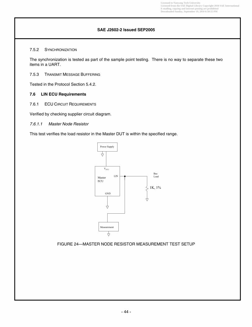
SAE J2602-2 Issued SEP2005
- 44 -
7.5.2 SYNCHRONIZATION
The synchronization is tested as part of the sample point testing. There is no way to separate these two items in a UART.
7.5.3 TRANSMIT MESSAGE BUFFERING
Tested in the Protocol Section 5.4.2.
7.6 LIN ECU Requirements
7.6.1 ECU CIRCUIT REQUIREMENTS
Verified by checking supplier circuit diagram.
7.6.1.1 Master Node Resistor
This test verifies the load resistor in the Master DUT is within the specified range.
Power Supply
VECU
LIN
GND
Measurement
Bus LoadMaster
ECU
1K, 1%
FIGURE 24—MASTER NODE RESISTOR MEASUREMENT TEST SETUP
Licensed to Nanyang Tech UniversityLicensed from the SAE Digital Library Copyright 2010 SAE International E-mailing, copying and internet posting are prohibitedDownloaded Sunday, September 19, 2010 6:50:55 PM
Author:Gilligan-SID:9234-GUID:35989776-155.69.4.4

SAE J2602-2 Issued SEP2005
- 45 -
TABLE 30—MASTER NODE RESISTOR MEASUREMENT TEST PLAN
DUT node as Master ECU Test case 7.6.1.1
Parameter VECU See Table 30 Test Steps
1. The voltages specified in Table 30 are applied. 2. The voltage of the LIN bus is measured.
Response See Table 30 Reference J2602-1 Section 7.6.1.1 and 7.6.1.2
# Test VECU VECU Slew rate Response
7.6.1.1 12.0V N/A The measured LIN bus voltage shall be between 6.3 V and 4.7 V.
7.6.1.2 Master Node Pull-Up Reverse Blocking Diode
See test in Section 7.6.1.1.
7.6.1.3 Master Node Capacitance
Test according to LIN Conformance Test Specification Physical Layer Version 1.0 of August 1, 2004 Section 3.1.3.
Instead of the 250 pF capacitor specified, the capacitor used for comparison shall be determined based on the module CTS and shall be either 272 pF, 778 pF or 2450 pF.
7.6.1.4 Slave Node Capacitance
Test according to LIN Conformance Test Specification Physical Layer Version 1.0 of August 1, 2004 Section 3.1.3.
Instead of the 250 pF capacitor specified, the capacitor used for comparison shall be 272 pF.
7.6.1.5 ESD Transient Suppressor
Verified by checking supplier circuit diagram. Total capacitance is measured in Section 7.6.1.3 or 7.6.1.4.
7.6.2 BOARD LAYOUT REQUIREMENTS
These are verified by a hardware design review of the module or test fixture.
7.7 Network Topology
7.7.1 LOSS OF ECU GROUND AT MASTER OR SLAVE NODE
This test verifies the leakage current when the DUT loses ground is within the specified range under maximum and minimum supply voltage conditions.
Licensed to Nanyang Tech UniversityLicensed from the SAE Digital Library Copyright 2010 SAE International E-mailing, copying and internet posting are prohibitedDownloaded Sunday, September 19, 2010 6:50:55 PM
Author:Gilligan-SID:9234-GUID:35989776-155.69.4.4

SAE J2602-2 Issued SEP2005
- 46 -
Remote-Controlled Power Supply
VECU
LIN
GND
Measurement
Bus LoadSlave/
MasterECU
FIGURE 25—LOSS OF ECU GROUND LEAKAGE CURRENT MEASUREMENT TEST SETUP
TABLE 31—LOSS OF ECU GROUND LEAKAGE CURRENT MEASUREMENT TEST PLAN
DUT node as Slave/Master ECU Test case 7.7.1.x (2 cases)
Parameter VECU Bus Load
See Table 31 1nF, 1kOhm Master test 1 nF, 20kOhm Slave test
Test Steps
1. The switch to the ground of the ECU is opened. 2. The voltages specified in Table 31 are applied. 3. The leakage current is measured by the equation (Vbatt-VLIN)/Rbus load.
Response See Table 31 Reference J2602-1 Section 7.7.1
# Test VECU VECU Slew Rate Response
7.7.1.1 8.0V N/A The measured leakage current shall be less than Ileak gnd specified in Table 6 of J2602-1
7.7.1.2 18.0V N/A The measured leakage current shall be less than Ileak gnd specified in Table 6 of J2602-1
7.7.2 LOSS OF ECU BATTERY
See Section 7.10.1.
7.7.3 BUS ELECTRICAL LOAD DISTRIBUTION
This is a system issue, not a component issue.
Licensed to Nanyang Tech UniversityLicensed from the SAE Digital Library Copyright 2010 SAE International E-mailing, copying and internet posting are prohibitedDownloaded Sunday, September 19, 2010 6:50:55 PM
Author:Gilligan-SID:9234-GUID:35989776-155.69.4.4

SAE J2602-2 Issued SEP2005
- 47 -
7.7.4 BUS WIRING TOPOLOGY CONFIGURATIONS
FYI.
7.7.5 BUS WIRING CONSTRAINTS
Guaranteed by system design.
7.7.6 BUS WIRING PRACTICES TO IMPROVE EMC PERFORMANCE
Guaranteed by system design.
7.7.7 BUS WIRING HARNESS AND ECU CONNECTORS
Shall be guaranteed by the connector supplier.
7.8 Master / Slave ESD Immunity
DUT circuit should be as specified in J2602-1 Figure 3 (Slave) or Figure 4 (Master).
The ECU LIN Bus I/O pin shall withstand the following electrostatic discharges without any damage to the ECU when subjected to the Ford EMC Test – Electrostatic Discharge Immunity test (Section 19). Use the requirements in Table 8 of J2602-1 unless otherwise specified in the CTS.
7.9 Master / Slave EMC Testing Requirements
DUT circuit should be as specified in J2602-1 Figure 3 (Slave) or Figure 4 (Master).
Testing using the below listed Ford EMC series of tests shall be used to assess the EMC performance of a LIN physical layer design. Required testing methods include the following EMC test specifications. 1. Test per Section 7.0 Radiated RF Emissions: RE310 2. Test per Section 10.3 RF Immunity Requirements 1 – 400 MHz: RI112, level 1. 3. Test per Section 10.4 RF Immunity Requirements 400 – 3100 MHz: RI114, level 1.
7.10 Fault Tolerant Modes
The Network shall meet the requirements as defined per the following failure modes:
Licensed to Nanyang Tech UniversityLicensed from the SAE Digital Library Copyright 2010 SAE International E-mailing, copying and internet posting are prohibitedDownloaded Sunday, September 19, 2010 6:50:55 PM
Author:Gilligan-SID:9234-GUID:35989776-155.69.4.4

SAE J2602-2 Issued SEP2005
- 48 -
7.10.1 ECU POWER LOSS – MASTER / SLAVE
This test verifies the leakage current when the DUT loses battery is within the specified range under maximum and minimum supply voltage conditions.
Remote-Controlled Power Supply
VECU
LIN
GND
Measurement
Bus LoadSlave/
MasterECU
FIGURE 26—ECU POWER LOSS LEAKAGE CURRENT MEASURMENT TEST SETUP
TABLE 32—ECU POWER LOSS LEAKAGE CURRENT MEASURMENT TEST PLAN
DUT node as Slave/Master ECU Test case 7.10.1.x (2 cases)
Parameter VECU Bus Load
See Table 32 1nF, 1kOhm Master test 1 nF, 20kOhm Slave test
Test Steps
1. The switch to the power supply of the ECU is opened. 2. The voltages specified below are applied. 3. The leakage current is measured by the equation (Vbatt-VLIN)/Rbus load.
Response See Table 32 Reference J2602-1 Section 7.10 #1
# Test VECU VECU Slew Rate Response 7.10.1.1 8.0V N/A The measured current shall be less than Ileak batt specified in
Table 6 of J2602-1 7.10.1.2 18.0V N/A The measured current shall be less than Ileak batt specified in
Table 6 of J2602-1
Licensed to Nanyang Tech UniversityLicensed from the SAE Digital Library Copyright 2010 SAE International E-mailing, copying and internet posting are prohibitedDownloaded Sunday, September 19, 2010 6:50:55 PM
Author:Gilligan-SID:9234-GUID:35989776-155.69.4.4

SAE J2602-2 Issued SEP2005
- 49 -
7.10.2 BUS WIRING SHORT TO GROUND – MASTER / SLAVE
This test verifies the impedence of the DUT after the LIN bus is shorted to ground is within 1% of the impedence prior to the shorting event.
Remote-Controlled Power Supply
VECU
LIN
GND
Measurement
Master/SlaveECU
FIGURE 27—BUS WIRING SHORT TO GROUND TEST SETUP
TABLE 33—BUS WIRING SHORT TO GROUND TEST PLAN
DUT node as Slave/Master ECU Test case 7.10.2
Test Steps
1. Measure the resistance between VECU and the LIN bus. 2. Close the Switch for 1 minute. 3. Open the switch and wait for 1 minute then measure the resistance between VECU and the
LIN bus. Response See Table 33 Reference J2602-1 Section 7.10 #2
# Test VECU VECU Slew Rate Response
7.10.2 18.0V N/A The resistance measured at the end of the test shall be within 1% of that measured at the start of the test.
Licensed to Nanyang Tech UniversityLicensed from the SAE Digital Library Copyright 2010 SAE International E-mailing, copying and internet posting are prohibitedDownloaded Sunday, September 19, 2010 6:50:55 PM
Author:Gilligan-SID:9234-GUID:35989776-155.69.4.4

SAE J2602-2 Issued SEP2005
- 50 -
7.10.3 BUS WIRING SHORT TO BATTERY
This test verifies the characteristics of the output driver of the DUT after the LIN bus is shorted to battery are the same as they were prior to the shorting event.
7.10.3.1 Master / Slave Device with TxD/RxD Accessible
Remote-Controlled Power Supply
VSUP
LIN
TxD
RxD
Pulse Generator
GND
Measurement
Bus Load
FIGURE 28—BUS WIRING SHORT TO BATTERY WITH TxD/RxD ACCESSIBLE TEST SETUP
TABLE 34—BUS WIRING SHORT TO BATTERY WITH TxD/RxD ACCESSIBLE TEST PLAN
DUT node as
RxD/TxD Accessible Device
Test case 7.10.3.1
Parameter VSUP Bus Load
See Table 34 1nF, 1kOhm
Test Steps
1. Set VSUP to 12 V. 2. The TxD line is driven with a 5.208kHz rectangular signal with a duty cycle of 50% and
an appropriate I/O voltage swing for the DUT (e.g. 5V, 3.3 V, etc.). 3. The DUT must be in operational / active mode 4. Capture a dominant pulse on the LIN bus transmitted by the DUT. 5. Set VSUP to 26.5 V. 6. Close the switch for 1 minute and then open it. 7. Set VSUP to 12 V. 8. Wait 10 seconds. 9. Capture a dominant pulse on the LIN bus transmitted by the DUT.
Response See Table 36 Reference J2602-1 Section 7.12.1
# Test VSUP Range VSUP Slew Rate Response
7.10.3.1 [12.0V & 26.5V]
N/A Compare the before and after dominant pulses. There should be no significant difference in rise time, fall time, output voltages or wave shape.
Licensed to Nanyang Tech UniversityLicensed from the SAE Digital Library Copyright 2010 SAE International E-mailing, copying and internet posting are prohibitedDownloaded Sunday, September 19, 2010 6:50:55 PM
Author:Gilligan-SID:9234-GUID:35989776-155.69.4.4

SAE J2602-2 Issued SEP2005
- 51 -
7.10.3.2 Device with TxD/RxD Not Accessible
7.10.3.2.1 Slave Device
Remote-Controlled Power Supply
VECU
LIN
LIN Tool
GND
Measurement
Bus Load
SlaveECU
FIGURE 29—BUS WIRING SHORT TO BATTERY WITH TxD/RxD NOT ACCESSIBLE TEST SETUP
TABLE 35—BUS WIRING SHORT TO BATTERY WITH TxD/RxD NOT ACCESSIBLE TEST PLAN
DUT node as Slave ECU Test case 7.10.3.2.1
Parameter VECU Bus Load
See Table 35 1nF, 1kOhm
Test Steps
1. Set VSUP to 12 V. 2. The DUT must be in operational / active mode 3. The LIN tool transmits a Targeted Reset (see Section 5.7.3) followed by a $3D
response to the Slave ECU. 4. Capture a dominant pulse on the LIN bus transmitted by the DUT. 5. Disconnect the LIN Tool. 6. Set VSUP to 26.5 V. 7. Close the switch for 1 minute and then open it. 8. Set VSUP to 12 V. 9. Reconnect the LIN Tool 10. Wait 10 seconds. 11. The LIN tool transmits a Targeted Reset (see Section 5.7.3) followed by a $3D
response to the Slave ECU. 12. Capture a dominant pulse on the LIN bus transmitted by the DUT.
Response See Table 35 Reference J2602-1 Section 7.10 #3
# Test VSUP Range VSUP Slew Rate Response 7.10.3.2.1 [12.0V &
26.5V] N/A Compare the before and after dominant pulses. There
should be no significant difference in rise time, fall time, output voltages or wave shape.
Licensed to Nanyang Tech UniversityLicensed from the SAE Digital Library Copyright 2010 SAE International E-mailing, copying and internet posting are prohibitedDownloaded Sunday, September 19, 2010 6:50:55 PM
Author:Gilligan-SID:9234-GUID:35989776-155.69.4.4

SAE J2602-2 Issued SEP2005
- 52 -
7.10.4 SHORT / OPEN IN OTHER CIRCUITS
This is NOT a requirement on the LIN device, but on the other devices in the DUT.
7.11 Ground Offset Voltage
Guaranteed by System Design.
7.12 Operating Battery Power Voltage Range
7.12.1 NORMAL BATTERY VOLTAGE POWER OPERATION
This test verifies the operating voltage range of the DUT.
7.12.1.1 Master / Slave Device with TxD/RxD Accessible
Remote-Controlled Power Supply
VSUP
LIN
TxD
RxD
Pulse Generator
GND
Measurement
Bus Load
FIGURE 30—NORMAL BATTERY VOLTAGE OPERATING RANGE WITH TxD/RxD ACCESSIBLE TEST SETUP
TABLE 36—NORMAL BATTERY VOLTAGE OPERATING RANGE WITH TxD/RxD ACCESSIBLE TEST PLAN
DUT node as
RxD/TxD Accessible Device
Test case 7.12.1.1.x(2 cases)
Parameter VSUP Bus Load
See Table 36 1nF, 1kOhm
Test Steps
1. A voltage ramp is set on the VSUP as defined on Table 36 2. The TxD line is driven with a 5.208kHz rectangular signal with a duty cycle of 50% and a
voltage swing of 5V. 3. The DUT must be in operational / active mode
Response See Table 36 Reference J2602-1 Section 7.12.1
Licensed to Nanyang Tech UniversityLicensed from the SAE Digital Library Copyright 2010 SAE International E-mailing, copying and internet posting are prohibitedDownloaded Sunday, September 19, 2010 6:50:55 PM
Author:Gilligan-SID:9234-GUID:35989776-155.69.4.4

SAE J2602-2 Issued SEP2005
- 53 -
TABLE 36—NORMAL BATTERY VOLTAGE OPERATING RANGE WITH TxD/RxD ACCESSIBLE TEST PLAN (CONTINUED)
# Test VSUP Range VSUP Slew Rate Response 7.12.1.1.1 [6.0V…18V] 0.5V/s The LIN pin shall follow TxD over the voltage range of
[7.0 to 18.0 V] The RxD pin shall follow TxD over the voltage range of [18.0 to 7.0 V]
7.12.1.1.2 [18V…6.0V] 0.5V/s The LIN pin shall follow TxD over the voltage range of [18.0 to 7.0 V] The RxD pin shall follow TxD over the voltage range of [7.0 to 18.0 V]
7.12.1.2 Device with TxD/RxD Not Accessible
7.12.1.2.1 Slave Device
Remote-Controlled Power Supply
VECU
LIN
LIN Tool
GND
Measurement
Bus Load
SlaveECU
FIGURE 31—NORMAL BATTERY VOLTAGE OPERATING RANGE WITH TxD/RxD NOT ACCESSIBLE TEST SETUP
TABLE 37—SLAVE NORMAL BATTERY VOLTAGE OPERATING RANGE WITH TxD/RxD NOT ACCESSIBLE TEST PLAN
DUT node as Slave ECU Test case 7.12.1.2.1.x(2 cases)
Parameter VECU Bus Load
See Table 37 1nF, 1kOhm
Test Steps
1. A voltage ramp is set on the VECU as defined on Table 37 2. The LIN tool transmits a Targeted Reset (see Section 5.7.3) followed by a $3D response
to the Slave ECU 3. The DUT must be in operational / active mode
Response See Table 37 Reference J2602-1 Section 7.12.1
Licensed to Nanyang Tech UniversityLicensed from the SAE Digital Library Copyright 2010 SAE International E-mailing, copying and internet posting are prohibitedDownloaded Sunday, September 19, 2010 6:50:55 PM
Author:Gilligan-SID:9234-GUID:35989776-155.69.4.4

SAE J2602-2 Issued SEP2005
- 54 -
TABLE 37—SLAVE NORMAL BATTERY VOLTAGE OPERATING RANGE WITH TxD/RxD NOT ACCESSIBLE TEST PLAN (CONTINUED)
# Test VECU Range VECU Slew Rate Response 7.12.1.2.1.1 [7.0V…18V] 0.5V/s The Slave ECU shall respond to the $3D request over the
voltage range of [8.0 to 18.0 V] 7.12.1.2.1.2 [18V…7.0V] 0.5V/s The Slave ECU shall respond to the $3D request over the
voltage range of [18.0 to 8.0 V]
7.12.1.2.2 Master Device
TABLE 38—MASTER NORMAL BATTERY VOLTAGE OPERATING RANGE WITH TxD/RxD NOT ACCESSIBLE TEST PLAN
DUT node as Master ECU Test case 7.12.1.2.2.x(2 cases)
Parameter VECU Bus Load
See Table 38 1nF, 20 kOhm
Test Steps
1. A voltage ramp is set on the VECU as defined on Table 38 2. The LIN tool transmits a Wake-up Request (see Section 7.2.1) 3. The DUT must respond with any message within 100 ms of receipt of the Wake-up
Request. 4. The LIN tool must stop transmission of the wake-up request.
Response See Table 37 Reference J2602-1 Section 7.12.1
# Test VECU Range VECU Slew Rate Response
7.12.1.2.2.1 [7.0V…18V] 0.5V/s The Master ECU shall respond to the Wake-up Request over the voltage range of [8.0 to 18.0 V]
7.12.1.2.2.2 [18V…7.0V] 0.5V/s The Master ECU shall respond to the Wake-up Request over the voltage range of [18.0 to 8.0 V]
7.12.2 BATTERY POWER OVER-VOLTAGE OPERATION
This test verifies the DUT either operates within the specification or goes into the passive mode when the supply voltage is between 18 and 26.5V.
7.12.2.1 Master / Slave Device with TxD/RxD Accessible
Repeat test from Section 7.12.1.1 with the parameters in Table 39.
TABLE 39—MASTER / SLAVE BATTERY OVER-VOLTAGE OPERATION WITH TxD/RxD ACCESSIBLE TEST PLAN
# Test VSUP Range VSUP Slew Rate Response 7.12.1.1.1 [18.0V…
26.5V] 0.5V/s If the LIN pin is not recessive, the r-d transition times and
the output voltages must meet the requirements specified in Table 16
7.12.1.1.2 [26.5V… 18V]
0.5V/s If the LIN pin is not recessive, the r-d transition times and the output voltages must meet the requirements specified in Table 16
Licensed to Nanyang Tech UniversityLicensed from the SAE Digital Library Copyright 2010 SAE International E-mailing, copying and internet posting are prohibitedDownloaded Sunday, September 19, 2010 6:50:55 PM
Author:Gilligan-SID:9234-GUID:35989776-155.69.4.4

SAE J2602-2 Issued SEP2005
- 55 -
7.12.2.2 Device with TxD/RxD Not Accessible
7.12.2.2.1 Slave Device
Repeat test from Section 7.12.1.2.1 with the parameters in Table 40.
TABLE 40—SLAVE BATTERY OVER-VOLTAGE OPERATION WITH TxD/RxD NOT ACCESSIBLE TEST PLAN
# Test VECU Range VECU Slew Rate Response 7.12.1.2.1.1 [18.0V…
26.5V] 0.5V/s If the LIN pin is not recessive, the r-d transition times and
the output voltages must meet the requirements specified in Table 16
7.12.1.2.1.2 [26.5V… 18V]
0.5V/s If the LIN pin is not recessive, the r-d transition times and the output voltages must meet the requirements specified in Table 16
7.12.2.2.2 Master Device
Repeat test from Section 7.12.1.2.2 with the parameters in Table 40.
7.12.3 LOW BATTERY VOLTAGE OPERATION
7.12.3.1 Master / Slave Device with TxD/RxD Accessible
Repeat test from Section 7.12.1.1 with the parameters in Table 41.
TABLE 41—MASTER / SLAVE LOW BATTERY OPERATION WITH TxD/RxD ACCESSIBLE TEST PLAN
# Test VSUP Range VSUP Slew Rate Response 7.12.1.1.1 [0V…7.0V] 0.5V/s If the LIN pin is not recessive, the r-d transition times and
the output voltages must meet the requirements specified in Table 16
7.12.1.1.2 [7.0V…0V] 0.5V/s If the LIN pin is not recessive, the r-d transition times and the output voltages must meet the requirements specified in Table 16
7.12.3.2 Device with TxD/RxD Not Accessible
7.12.3.2.1 Slave Device
Repeat test from Section 7.12.1.2.1 with the parameters in Table 42.
Licensed to Nanyang Tech UniversityLicensed from the SAE Digital Library Copyright 2010 SAE International E-mailing, copying and internet posting are prohibitedDownloaded Sunday, September 19, 2010 6:50:55 PM
Author:Gilligan-SID:9234-GUID:35989776-155.69.4.4

SAE J2602-2 Issued SEP2005
- 56 -
TABLE 42—SLAVE LOW BATTERY OPERATION WITH TxD/RxD NOT ACCESSIBLE TEST PLAN
# Test VECU Range VECU Slew Rate Response 7.12.1.2.1.1 [0V…8.0V] 0.5V/s If the LIN pin is not recessive, the r-d transition times and
the output voltages must meet the requirements specified in Table 16
7.12.1.2.1.2 [8.0V…0V] 0.5V/s If the LIN pin is not recessive, the r-d transition times and the output voltages must meet the requirements specified in Table 16
7.12.3.2.2 Master Device
Repeat test from Section 7.12.1.2.2 with the parameters in Table 42.
7.12.4 BATTERY OFFSET VOLTAGE
Guaranteed by System Design.
7.12.5 REVERSE BATTERY BLOCKING DIODE
Guaranteed by Module Design.
7.13 Environmental Requirements
Operating requirement guaranteed by IC design.
7.13.1 TRANSMIT OPERATING CONDITIONS
7.13.1.1 Master Device
Verifiable by IC manufacturer qualification testing.
7.13.1.2 Slave Device
Verifiable by IC manufacturer qualification testing.
7.13.1.2.1 Stand-Alone Transceivers
Verifiable by IC manufacturer qualification testing.
7.13.1.2.2 Integrated Transceivers
Verifiable by IC manufacturer qualification testing.
PREPARED BY THE SAE J2602 LIN TASK FORCE OF THE SAE VEHICLE ARCHITECTURE FOR DATA COMMUNICATION STANDARDS COMMITTEE
Licensed to Nanyang Tech UniversityLicensed from the SAE Digital Library Copyright 2010 SAE International E-mailing, copying and internet posting are prohibitedDownloaded Sunday, September 19, 2010 6:50:55 PM
Author:Gilligan-SID:9234-GUID:35989776-155.69.4.4

SAE J2602-2 Issued SEP2005
- 57 -
APPENDIX A LIN DEVICE SUPPLIERS
The following is a list of known device suppliers as of the date of publication. Please visit the following websites for information on the available devices. AMIS – www.amis.com AMS – www.austriamicrosystems.com Infineon – www.infineon.com Melexis – www.melexis.com Microchip – www.microchip.com Motorola – www.motorola.com/semiconductors/lin ON Semiconductor – www.onsemi.com Philips – www.semiconductors.philips.com Renesas – www.renesas.com/eng STMicroelectronics – www.ST.com
Licensed to Nanyang Tech UniversityLicensed from the SAE Digital Library Copyright 2010 SAE International E-mailing, copying and internet posting are prohibitedDownloaded Sunday, September 19, 2010 6:50:55 PM
Author:Gilligan-SID:9234-GUID:35989776-155.69.4.4